WO2015079939A1 - External-resonator-type light emitting device - Google Patents
External-resonator-type light emitting device Download PDFInfo
- Publication number
- WO2015079939A1 WO2015079939A1 PCT/JP2014/080301 JP2014080301W WO2015079939A1 WO 2015079939 A1 WO2015079939 A1 WO 2015079939A1 JP 2014080301 W JP2014080301 W JP 2014080301W WO 2015079939 A1 WO2015079939 A1 WO 2015079939A1
- Authority
- WO
- WIPO (PCT)
- Prior art keywords
- grating
- wavelength
- optical waveguide
- light source
- laser
- Prior art date
Links
Images


Classifications
-
- H—ELECTRICITY
- H01—ELECTRIC ELEMENTS
- H01S—DEVICES USING THE PROCESS OF LIGHT AMPLIFICATION BY STIMULATED EMISSION OF RADIATION [LASER] TO AMPLIFY OR GENERATE LIGHT; DEVICES USING STIMULATED EMISSION OF ELECTROMAGNETIC RADIATION IN WAVE RANGES OTHER THAN OPTICAL
- H01S5/00—Semiconductor lasers
- H01S5/10—Construction or shape of the optical resonator, e.g. extended or external cavity, coupled cavities, bent-guide, varying width, thickness or composition of the active region
- H01S5/14—External cavity lasers
- H01S5/141—External cavity lasers using a wavelength selective device, e.g. a grating or etalon
-
- G—PHYSICS
- G02—OPTICS
- G02B—OPTICAL ELEMENTS, SYSTEMS OR APPARATUS
- G02B6/00—Light guides; Structural details of arrangements comprising light guides and other optical elements, e.g. couplings
- G02B6/10—Light guides; Structural details of arrangements comprising light guides and other optical elements, e.g. couplings of the optical waveguide type
- G02B6/12—Light guides; Structural details of arrangements comprising light guides and other optical elements, e.g. couplings of the optical waveguide type of the integrated circuit kind
- G02B6/122—Basic optical elements, e.g. light-guiding paths
- G02B6/124—Geodesic lenses or integrated gratings
-
- H—ELECTRICITY
- H01—ELECTRIC ELEMENTS
- H01S—DEVICES USING THE PROCESS OF LIGHT AMPLIFICATION BY STIMULATED EMISSION OF RADIATION [LASER] TO AMPLIFY OR GENERATE LIGHT; DEVICES USING STIMULATED EMISSION OF ELECTROMAGNETIC RADIATION IN WAVE RANGES OTHER THAN OPTICAL
- H01S5/00—Semiconductor lasers
- H01S5/02—Structural details or components not essential to laser action
- H01S5/022—Mountings; Housings
- H01S5/023—Mount members, e.g. sub-mount members
- H01S5/02325—Mechanically integrated components on mount members or optical micro-benches
- H01S5/02326—Arrangements for relative positioning of laser diodes and optical components, e.g. grooves in the mount to fix optical fibres or lenses
-
- H—ELECTRICITY
- H01—ELECTRIC ELEMENTS
- H01S—DEVICES USING THE PROCESS OF LIGHT AMPLIFICATION BY STIMULATED EMISSION OF RADIATION [LASER] TO AMPLIFY OR GENERATE LIGHT; DEVICES USING STIMULATED EMISSION OF ELECTROMAGNETIC RADIATION IN WAVE RANGES OTHER THAN OPTICAL
- H01S5/00—Semiconductor lasers
- H01S5/02—Structural details or components not essential to laser action
- H01S5/028—Coatings ; Treatment of the laser facets, e.g. etching, passivation layers or reflecting layers
- H01S5/0287—Facet reflectivity
-
- H—ELECTRICITY
- H01—ELECTRIC ELEMENTS
- H01S—DEVICES USING THE PROCESS OF LIGHT AMPLIFICATION BY STIMULATED EMISSION OF RADIATION [LASER] TO AMPLIFY OR GENERATE LIGHT; DEVICES USING STIMULATED EMISSION OF ELECTROMAGNETIC RADIATION IN WAVE RANGES OTHER THAN OPTICAL
- H01S5/00—Semiconductor lasers
- H01S5/10—Construction or shape of the optical resonator, e.g. extended or external cavity, coupled cavities, bent-guide, varying width, thickness or composition of the active region
- H01S5/1021—Coupled cavities
-
- H—ELECTRICITY
- H01—ELECTRIC ELEMENTS
- H01S—DEVICES USING THE PROCESS OF LIGHT AMPLIFICATION BY STIMULATED EMISSION OF RADIATION [LASER] TO AMPLIFY OR GENERATE LIGHT; DEVICES USING STIMULATED EMISSION OF ELECTROMAGNETIC RADIATION IN WAVE RANGES OTHER THAN OPTICAL
- H01S5/00—Semiconductor lasers
- H01S5/10—Construction or shape of the optical resonator, e.g. extended or external cavity, coupled cavities, bent-guide, varying width, thickness or composition of the active region
- H01S5/1039—Details on the cavity length
-
- H—ELECTRICITY
- H01—ELECTRIC ELEMENTS
- H01S—DEVICES USING THE PROCESS OF LIGHT AMPLIFICATION BY STIMULATED EMISSION OF RADIATION [LASER] TO AMPLIFY OR GENERATE LIGHT; DEVICES USING STIMULATED EMISSION OF ELECTROMAGNETIC RADIATION IN WAVE RANGES OTHER THAN OPTICAL
- H01S5/00—Semiconductor lasers
- H01S5/20—Structure or shape of the semiconductor body to guide the optical wave ; Confining structures perpendicular to the optical axis, e.g. index or gain guiding, stripe geometry, broad area lasers, gain tailoring, transverse or lateral reflectors, special cladding structures, MQW barrier reflection layers
- H01S5/22—Structure or shape of the semiconductor body to guide the optical wave ; Confining structures perpendicular to the optical axis, e.g. index or gain guiding, stripe geometry, broad area lasers, gain tailoring, transverse or lateral reflectors, special cladding structures, MQW barrier reflection layers having a ridge or stripe structure
- H01S5/2202—Structure or shape of the semiconductor body to guide the optical wave ; Confining structures perpendicular to the optical axis, e.g. index or gain guiding, stripe geometry, broad area lasers, gain tailoring, transverse or lateral reflectors, special cladding structures, MQW barrier reflection layers having a ridge or stripe structure by making a groove in the upper laser structure
-
- H—ELECTRICITY
- H01—ELECTRIC ELEMENTS
- H01S—DEVICES USING THE PROCESS OF LIGHT AMPLIFICATION BY STIMULATED EMISSION OF RADIATION [LASER] TO AMPLIFY OR GENERATE LIGHT; DEVICES USING STIMULATED EMISSION OF ELECTROMAGNETIC RADIATION IN WAVE RANGES OTHER THAN OPTICAL
- H01S2301/00—Functional characteristics
- H01S2301/16—Semiconductor lasers with special structural design to influence the modes, e.g. specific multimode
- H01S2301/163—Single longitudinal mode
Definitions
- the present invention relates to an external resonator type light emitting device.
- a Fabry-Perot (FP) type is generally used in which an optical resonator is sandwiched between mirrors formed on both end faces of an active layer.
- FP Fabry-Perot
- DFB distributed feedback
- DBR distributed reflection
- the DBR laser realizes a resonator by forming irregularities on the waveguide surface on the extension of the waveguide of the active layer to form a mirror by Bragg reflection (Patent Document 1 (Japanese Patent Laid-Open No. 49-128689): Patent) Document 2 (Japanese Patent Laid-Open No. 56-148880). Since this laser is provided with diffraction gratings at both ends of the optical waveguide layer, the light emitted from the active layer propagates through the optical waveguide layer, a part of which is reflected by this diffraction grating, returns to the current injection part, and is amplified. Is done. Since only one wavelength of light reflects in the direction determined from the diffraction grating, the wavelength of the laser light is constant.
- an external resonator type semiconductor laser has been developed in which a diffraction grating is a component different from a semiconductor and a resonator is formed externally.
- This type of laser is a laser with good wavelength stability, temperature stability, and controllability.
- the external resonator includes a fiber Bragg grating (FBG) (Non-patent Document 1) and a volume hologram grating (VHG) (Non-patent Document 2). Since the diffraction grating is composed of a separate member from the semiconductor laser, it has the feature that the reflectance and resonator length can be individually designed, and it is not affected by the temperature rise due to heat generation due to current injection. Can be better. Moreover, since the temperature change of the refractive index of the semiconductor is different, the temperature stability can be improved by designing it together with the resonator length.
- Patent Document 6 Japanese Patent Laid-Open No. 2002-134833 discloses an external resonator type laser using a grating formed in a quartz glass waveguide. This is to provide a frequency stabilized laser that can be used in an environment where the room temperature changes greatly (for example, 30 ° C. or more) without a temperature controller. Further, it is described that a temperature-independent laser in which mode hopping is suppressed and the oscillation frequency is not temperature-dependent is provided.
- Patent Document 7 Japanese Patent Laid-Open No. 2010-171252 discloses an optical waveguide having SiO 2 , SiO 1-x N x (x is 0.55 to 0.65), or Si and SiN as a core layer, and the optical waveguide Discloses an external cavity laser in which a grating is formed.
- This is an external cavity laser that keeps the oscillation wavelength constant without precise temperature control.
- it is a precondition that the temperature change rate of the reflection wavelength of the diffraction grating (temperature coefficient of the Bragg reflection wavelength) is reduced.
- the power stability can be realized by setting the laser oscillation to the longitudinal mode multimode.
- Patent Document 8 discloses a laser as an external resonator using a grating formed on an optical waveguide made of quartz, InP, GaAs, LiNbO 3 , LiTaO 3 , or polyimide resin. This is because the reflectivity at the light exit surface of the semiconductor laser as the light source is the effective reflectivity Re (substantially 0.1 to 38.4%), and the laser oscillation is set to the longitudinal mode multimode. It is described that power stability can be realized.
- Non-Patent Document 1 mentions a mode hop mechanism that impairs the wavelength stability associated with a temperature rise, and an improvement measure thereof.
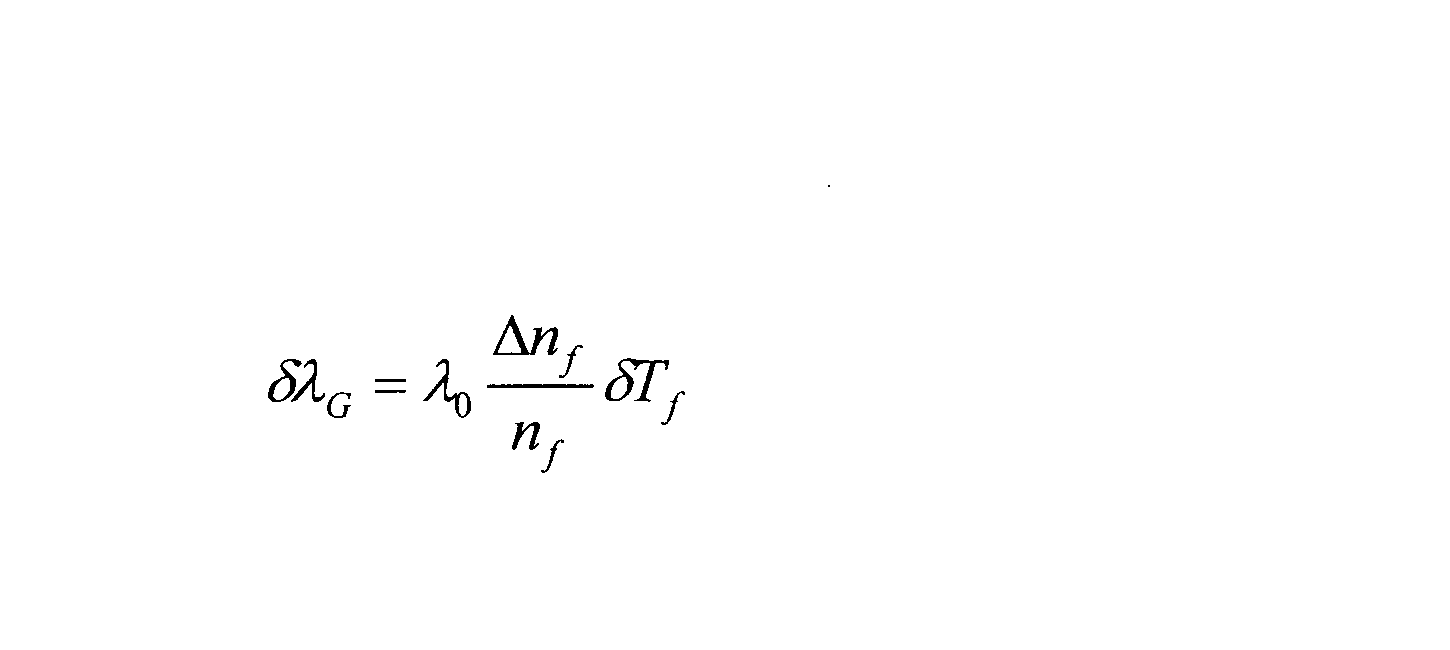
- the wavelength variation ⁇ s of the external cavity laser due to the temperature is the change in refractive index ⁇ na of the active layer region of the semiconductor, the length La of the active layer, the refractive index variation ⁇ nf of the FBG region, the length Lf, and the temperature variation ⁇ Ta.
- ⁇ Tf is expressed by the following equation from the standing wave condition.
- ⁇ 0 represents the grating reflection wavelength in the initial state.
- ⁇ G the change ⁇ G in the grating reflection wavelength is expressed by the following equation.
- the longitudinal mode interval ⁇ is approximately expressed by the following equation.
- Equation 5 is established.
- Mode hop is a phenomenon in which the oscillation mode (longitudinal mode) in the resonator changes from one mode to another.
- the gain and resonator conditions change, the laser oscillation wavelength changes, and the problem arises that optical power fluctuates, which is called kink. Therefore, in the case of an FP type GaAs semiconductor laser, the wavelength usually changes with a temperature coefficient of 0.3 nm / ° C., but when a mode hop occurs, a larger fluctuation occurs. At the same time, the output fluctuates by 5% or more.
- Patent Document 6 in order to make the temperature independent, the conventional resonator structure is left as it is, and stress is applied to the optical waveguide layer to compensate for the temperature coefficient due to thermal expansion, thereby realizing temperature independence. is doing. For this reason, a metal plate is attached to the element, and a layer for adjusting the temperature coefficient is added to the waveguide. For this reason, there exists a problem that a resonator structure becomes still larger.
- An object of the present invention is to suppress mode hopping, increase wavelength stability, and suppress fluctuations in optical power without using a Peltier element.
- the present invention is an external resonator type light emitting device that includes a light source that oscillates a semiconductor laser light alone, and a grating element that constitutes the light source and an external resonator, and oscillates in a single mode
- the light source includes an active layer that oscillates the semiconductor laser light
- the grating element includes an optical waveguide having an incident surface on which the semiconductor laser light is incident and an output surface that emits outgoing light of a desired wavelength, a Bragg grating formed in the optical waveguide, and the incident surface and the Bragg grating. Is provided, and the following equations (1) to (5) are satisfied.
- ⁇ G is the full width at half maximum at the peak of the Bragg reflectivity.
- L b is the length of the Bragg grating.
- L a is the length of the active layer.
- n b is the refractive index of the material constituting the Bragg grating.
- d ⁇ G / dT is the temperature coefficient of the Bragg wavelength
- d ⁇ TM / dT is the temperature coefficient of the wavelength that satisfies the phase condition of the external cavity laser.
- quartz has a small temperature coefficient of refractive index, so d ⁇ G / dT is small and
- a material having a refractive index of 1.8 or more of the waveguide substrate on which the grating is formed is used.
- the temperature coefficient of the refractive index can be increased and d ⁇ G / dT can be increased. Therefore,
- L WG 600 ⁇ m (6) 1 ⁇ m ⁇ L g ⁇ 10 ⁇ m (7) 20 ⁇ m ⁇ L m ⁇ 100 ⁇ m (8)
- LWG is the length of the grating element.
- L g is the distance between the exit surface of the light source and the entrance surface of the optical waveguide.
- L m is the length of the propagation unit.
- mode hops can be suppressed, wavelength stability can be increased, and optical power fluctuations can be suppressed without using a Peltier element.
- FIG. 1 is a schematic diagram of an external resonator type light emitting device.
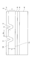
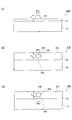
- FIG. 2 is a cross-sectional view of the grating element.
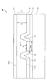
- FIG. 3 is a perspective view schematically showing the grating element.
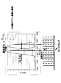
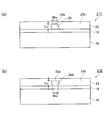
- FIG. 4 is a cross-sectional view of another grating element.
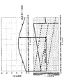
- FIG. 5 is a diagram for explaining a mode hop mode according to a conventional example.
- FIG. 6 is a diagram for explaining a mode hop mode according to a conventional example.
- FIG. 7 is a diagram illustrating a mode hop mode according to an example of the present invention.
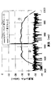
- FIG. 8 shows the spectrum of the light amount of the light source and the spectrum of the device obtained by adding a grating element to this light source in Example 2.
- FIG. 8 shows the spectrum of the light amount of the light source and the spectrum of the device obtained by adding a grating element to this light source in Example 2.
- FIG. 8 shows the spectrum of the light amount of the light source and the spectrum of the device obtained by adding a
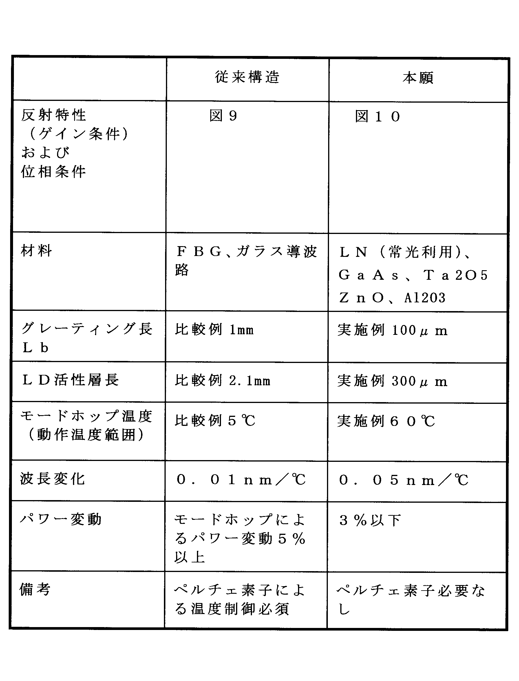
- FIG. 9 shows reflection characteristics (gain conditions) and phase conditions in a conventional structure.
- FIG. 10 shows reflection characteristics (gain conditions) and phase conditions in the structure of the present invention.
- (A), (b), (c) is a schematic diagram which shows the cross section of the grating elements 21A, 21B, and 21C using the elongated striped optical waveguides 30 and 30A, respectively.
- (A), (b) is a schematic diagram which shows the cross section of the grating elements 21D and 21E using the elongate stripe-shaped optical waveguides 30 and 30A, respectively.
- An external resonator type light emitting device 1 schematically shown in FIG. 1 includes a light source 2 that oscillates a semiconductor laser beam and a grating element 9.
- the light source 2 and the grating element 9 are mounted on the common substrate 3.
- the light source 2 includes an active layer 5 that oscillates semiconductor laser light.
- the active layer 5 is provided on the substrate 4.
- the light source 2 is a light source capable of laser oscillation independently. This means that the light source 2 oscillates by itself even without a grating element.
- the light source 2 preferably has a single mode oscillation in the longitudinal mode when lasing alone.
- the reflection characteristics can be wavelength-dependent. Therefore, by controlling the shape of the wavelength characteristics, the light source 2 is independent and the longitudinal mode is multimode. Even if it oscillates, it can oscillate in a single mode as an external resonator type laser.
- a high reflection film 6 is provided on the outer end face of the substrate 4, and a reflection film 7 ⁇ / b> A is formed on the end face on the grating element side.
- the grating element 7 is provided with an optical material layer 11 having an incident surface 11 a on which the semiconductor laser light A is incident and an emission surface 11 b that emits the emitted light B having a desired wavelength. . C is reflected light.
- a Bragg grating 12 is formed in the optical material layer 11.
- a propagation part 13 without a diffraction grating is provided between the incident surface 11 a of the optical material layer 11 and the Bragg grating 12, and the propagation part 13 faces the active layer 5 with a gap 14 therebetween.
- Reference numeral 7B denotes an antireflective film provided on the incident surface side of the optical material layer 11
- reference numeral 7C denotes an antireflective film provided on the output surface side of the optical material layer 11.
- the optical material layer 11 is a ridge-type optical waveguide and is provided on the substrate 10.
- the optical material layer 11 may be formed on the same surface as the Bragg grating 12 or may be formed on an opposite surface.
- the reflectivity of the Bragg grating is larger than the reflectivity of the emission end of the light source, the reflectivity of the entrance surface of the grating element, and the reflectivity of the exit surface of the grating element.
- the reflectance of the incident surface of the grating element and the reflectance of the exit surface of the grating element are preferably 0.1% or less.
- the reflectance of the non-reflective layer may be a value smaller than the grating reflectance, and is preferably 0.1% or less. However, as long as the reflectance at the end face is smaller than the grating reflectance, the non-reflective layer may be omitted and a reflective film may be used.
- the optical material layer 11 is formed on the substrate 10 via the adhesive layer 15 and the lower buffer layer 16, and the upper buffer layer 17 is formed on the optical material layer 11. ing.
- a pair of ridge grooves 19 are formed in the optical material layer 11, and a ridge-type optical waveguide 18 is formed between the ridge grooves.
- the Bragg grating may be formed on the flat surface 11a or may be formed on the 11b surface. From the viewpoint of reducing the shape variation of the Bragg grating and the ridge groove, it is preferable that the Bragg grating and the ridge groove 19 are provided on the opposite side of the substrate by forming the Bragg grating on the surface 11a.
- the optical material layer 11 is formed on the substrate 10 via the adhesive layer 15 and the lower buffer layer 16, and the upper buffer layer 17 is formed on the optical material layer 11. Yes.
- a pair of ridge grooves 19 are formed on the substrate 10 side of the optical material layer 11, and a ridge-type optical waveguide 18 is formed between the ridge grooves 19.
- the Bragg grating may be formed on the flat surface 11a side, or may be formed on the 11b surface having the ridge groove.
- the Bragg grating and the ridge groove 19 are provided on the opposite side of the substrate by forming the Bragg grating on the flat surface 11a surface side.
- the upper buffer layer 17 may be omitted, and in this case, the air layer can directly contact the grating.
- the difference in refractive index can be increased without the presence of a grating groove, and the reflectance can be increased with a short grating length.
- the oscillation wavelength of the laser light is determined by the wavelength reflected by the grating. If the reflected light from the grating and the reflected light from the end face of the active layer 5 on the grating element side exceed the laser gain threshold, the oscillation condition is satisfied. Thereby, a laser beam with high wavelength stability can be obtained.
- the feedback amount from the grating may be increased.
- the reflectance of the grating is preferably larger than the reflectance at the end face of the active layer 5.
- a laser with a highly reliable GaAs-based or InP-based material is suitable.
- a GaAs laser that oscillates near a wavelength of 1064 nm is used. Since GaAs-based and InP-based lasers have high reliability, a light source such as a one-dimensionally arranged laser array can be realized. Since the temperature change of the Bragg wavelength increases as the wavelength becomes longer, the laser oscillation wavelength is particularly preferably 990 nm or less in order to improve the wavelength stability.
- the laser oscillation wavelength is particularly preferably 780 nm or more in order to improve the wavelength stability.
- the material and wavelength of the active layer can be selected as appropriate.
- a ridge-type optical waveguide is obtained by, for example, physical processing and molding by cutting with an outer peripheral blade or laser ablation processing.
- the buffer layer can function as a cladding layer of the optical waveguide.
- the refractive index of the buffer layer is preferably lower than the refractive index of the optical material layer, and the refractive index difference is preferably 0.2 or more, and more preferably 0.4 or more.
- Bragg grating can be formed by physical or chemical etching as follows.
- a metal film such as Ni or Ti is formed on a high refractive index substrate, and windows are periodically formed by photolithography to form an etching mask. Thereafter, periodic grating grooves are formed by a dry etching apparatus such as reactive ion etching. Finally, it can be formed by removing the metal mask.
- one or more metals selected from the group consisting of magnesium (Mg), zinc (Zn), scandium (Sc), and indium (In) are used to further improve the optical damage resistance of the optical waveguide. Elements may be included, in which case magnesium is particularly preferred.
- the crystal can contain a rare earth element as a doping component. As the rare earth element, Nd, Er, Tm, Ho, Dy, and Pr are particularly preferable.
- the material of the adhesive layer may be an inorganic adhesive, an organic adhesive, or a combination of an inorganic adhesive and an organic adhesive.
- the optical material layer 11 may be formed by forming a film on a supporting substrate by a thin film forming method. Examples of such a thin film forming method include sputtering, vapor deposition, and CVD. In this case, the optical material layer 11 is directly formed on the support substrate, and the above-described adhesive layer does not exist.
- the thickness of the optical material layer is more preferably 0.5 to 3.0 ⁇ m.
- the specific material of the support substrate is not particularly limited, and examples thereof include glass such as lithium niobate, lithium tantalate, and quartz glass, quartz, and Si.
- the reflectance of the non-reflective layer must be less than or equal to the grating reflectivity.
- a film laminated with an oxide such as silicon dioxide or tantalum pentoxide, or metal is also used. Is possible.
- each end face of the light source element and the grating element may be cut obliquely in order to suppress the end face reflection.
- the grating element and the support substrate are bonded and fixed in the example of FIG. 2, they may be directly bonded.
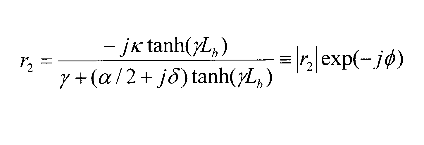
- the oscillation condition of the semiconductor laser is determined by gain condition ⁇ phase condition as shown in the following equation.
- ⁇ a and ⁇ b are the loss coefficients of the active layer and the grating layer, respectively
- La and Lb are the lengths of the active layer and the grating layer, respectively
- r1 and r2 are the mirror reflectivities (r2 is the grating)
- Cout is a coupling loss between the grating element and the light source
- ⁇ t g th is a gain threshold of the laser medium
- ⁇ 1 is a phase change amount by the laser side reflection mirror
- the gain condition is determined by the grating. For this reason, in the comparison table, the gain condition can be considered only by the grating.
- phase condition is expressed by the following equation from the equation (2-1). However, ⁇ 1 is zero.
- the external cavity laser has a feature of high wavelength stability.
- the temperature change rate of the refractive index ⁇ nf is as small as 1 ⁇ 10 -5 / °C
- the equivalent refractive index of the light source is 3.6
- the temperature change of the refractive index is 3 ⁇ 10 -4 / ° C
- the spectral waveform of the laser light thus laser-oscillated has a line width of 0.2 nm or less.
- the laser oscillation wavelength by an external resonator at room temperature of 25 ° C. should be shorter than the center wavelength of the grating reflectivity. preferable. In this case, as the temperature rises, the laser oscillation wavelength shifts to the longer wavelength side and laser oscillation occurs on the longer wavelength side than the center wavelength of the grating reflectivity.
- the laser oscillation wavelength by the external resonator at room temperature of 25 ° C. is longer than the oscillation wavelength of the light source 2 at the same temperature. It is preferable to oscillate at. In this case, as the temperature rises, the laser oscillation wavelength by the external resonator oscillates on the short wavelength side with respect to the oscillation wavelength of the light source 2.
- the difference between the laser oscillation wavelength by the external resonator at room temperature and the oscillation wavelength of the light source 2 is preferably 0.5 nm or more, and may be 2 nm or more from the viewpoint of widening the temperature tolerance of laser oscillation. However, if the wavelength difference is increased too much, the temperature variation of the power increases, so from this viewpoint, it is preferably 10 nm or less, and more preferably 6 nm or less.
- ⁇ G TM is a wavelength interval (longitudinal mode interval) that satisfies the phase condition of the external cavity laser.
- T mh is about 5 ° C. For this reason, mode hops are likely to occur. Therefore, when a mode hop occurs, the power fluctuates based on the reflection characteristics of the grating and fluctuates by 5% or more.
- the conventional external cavity laser using the glass waveguide or FBG performs temperature control using the Peltier element.
- the present invention uses a grating element having a small denominator of the equation (2-4) as a precondition.
- the denominator of formula (2-4) must be 0.03 nm / ° C or less.
- Specific materials include gallium arsenide (GaAs), lithium niobate (LiNbO 3 ), and tantalum oxide (Ta 2 O). 5 ), zinc oxide (ZnO), and alumina oxide (Al 2 O 3 ) are preferable.
- ⁇ G is designed to be about 1.3 nm, and the length of the active layer is 250 ⁇ m so that there are two wavelengths within ⁇ G that satisfy the phase condition.
- ⁇ G TM is, for example, 1.2 nm, T mh is 60 ° C., and the operating temperature range can be widened.
- FIG. 7 shows an example of this.
- the spectral width of the output laser oscillated under such conditions is 0.1 nm or less.
- the oscillation wavelength changes at 0.05 nm / ° C. based on the temperature characteristics of the grating with respect to the temperature change, but mode hopping can be made difficult to occur.
- the grating length Lb is set to 100 ⁇ m in order to increase the ⁇ lambda G
- La in order to increase the ⁇ G TM is set to 250 [mu] m.
- FIG. 6 The present application realizes temperature independence by bringing the temperature coefficient of the grating wavelength and the temperature coefficient of the longitudinal mode close to each other. For this reason, the resonator structure can be made compact and an additional one is unnecessary.
- each parameter is described as follows, and each is in the category of the prior art.
- ⁇ ⁇ G 0.4nm Vertical mode interval
- ⁇ G TM 0.2nm Grating length
- Lb 3mm
- the full width at half maximum ⁇ G at the peak of the Bragg reflectance is set to 0.8 nm or more (Formula 1).
- ⁇ G is the Bragg wavelength. That is, as shown in FIGS. 5, 6, and 7, when the reflection wavelength by the Bragg grating is taken on the horizontal axis and the reflectance is taken on the vertical axis, the wavelength at which the reflectance is maximized is the Bragg wavelength. In peak centered at the Bragg wavelength, the difference between the two wavelengths at which the reflectance becomes half the peak full width at half maximum [Delta] [lambda] G.
- the full width at half maximum ⁇ G at the Bragg reflectivity peak is set to 0.8 nm or more is to make the reflectivity peak broad as shown in FIG. From this viewpoint, it is preferable to be at least 1.2nm full width at half maximum [Delta] [lambda] G, it is further preferable to 1.5nm or more. Further, it is preferable that less 5nm a full width at half maximum [Delta] [lambda] G, more preferably to 3nm or less, it is preferable to 2nm or less.
- the length L b of the Bragg grating to 500 ⁇ m or less (equation 2).
- the length L b of the Bragg grating is a grating length in the direction of the optical axis of the light propagating through the optical waveguide. Be shorter than the Bragg grating length L b below the conventional 500 ⁇ m is a premise of the design concept of the present invention. From this viewpoint, it is more preferable to the Bragg grating length L b and 300 ⁇ m or less. Further, L b is more preferably set to 200 ⁇ m or less.
- the length of the active layer L a also a 500 ⁇ m or less (equation 3). It is also a prerequisite for the design concept of the present invention made shorter than the conventional length L a of the active layer. From this viewpoint, it is more preferable to set the length L a of the active layer and 300 ⁇ m or less.
- the length L a of the active layer is preferably set at 150 ⁇ m or more.
- Refractive index n b of the material of the Bragg grating is 1.8 or more (Equation 4).
- a material having a lower refractive index such as quartz, has been generally used.
- the refractive index of the material constituting the Bragg grating is increased. The reason for this is that a material with a large refractive index has a large temperature change in the refractive index, so that T mh in equation (2-4) can be increased and the temperature coefficient d ⁇ G / dT of the grating can be increased. It is. From this viewpoint, nb is more preferably 1.9 or more.
- n b is not particularly, although the grating pitch is 4 or less from the formation becomes too small it is difficult, it is preferably more than 3.6 or less. From the same viewpoint, the equivalent refractive index of the optical waveguide is preferably 3.3 or less.
- d ⁇ G / dT is the temperature coefficient of the Bragg wavelength.
- D ⁇ TM / dT is a temperature coefficient of the wavelength that satisfies the phase condition of the external cavity laser.
- ⁇ TM is a wavelength that satisfies the phase condition of the external cavity laser, that is, a wavelength that satisfies the above-described phase condition of (Equation 2.3). This is called “vertical mode” in this specification.
- ⁇ G TM is a wavelength interval (longitudinal mode interval) that satisfies the phase condition of the external cavity laser.
- lambda TM Since the plurality of, means the difference of a plurality of lambda TM. Previously used ⁇ lambda equals ⁇ G TM, ⁇ s is equal to lambda TM.
- the numerical value of the formula (5) is more preferably 0.025 or less.
- L WG The length of the grating element L WG also to 600 ⁇ m or less (formula 6). It is a premise of the present invention to make this as short as Lb. From this viewpoint, L WG is preferably 400 ⁇ m or less, more preferably 300 ⁇ m or less. Further, LWG is preferably 50 ⁇ m or more.
- the light source and the grating element are directly optically connected, and a resonator structure is formed between the outer end surface opposite to the emission surface of the active layer and the Bragg grating, and the active layer
- the length between the outer end face of the light source and the exit end point of the Bragg grating is 900 ⁇ m or less. Since light is gradually reflected at the grating portion, it is not possible to observe a clear reflection point like a reflection mirror. Although the effective reflection point can be defined mathematically, it exists on the laser side from the end point on the emission side of the Bragg grating. For this reason, in the present application, the length of the resonator is defined at the end point on the emission side.
- the length between the outer end face of the active layer and the exit end point of the Bragg grating is more preferably 800 ⁇ m or less, and particularly preferably 700 ⁇ m or less. From the viewpoint of increasing the laser output, this length is preferably 300 ⁇ m or more.
- the optical waveguide is a ridge type optical waveguide including a ridge portion and at least a pair of ridge grooves forming the ridge portion.
- the optical material is left under the ridge groove, and extending portions made of the optical material are also formed outside the ridge groove.
- the strip-shaped elongated core can be formed by removing the optical material under the ridge groove.
- the ridge-type optical waveguide is composed of an elongated core made of an optical material, and the cross section of the core forms a convex figure.
- a buffer layer (cladding layer) and an air layer exist around the core, and the buffer layer and the air layer function as a clad.
- the convex figure means that a line segment connecting any two points of the outer contour line of the core cross section is located inside the outer contour line of the core cross section.
- Examples of such figures include triangles, quadrangles, hexagons, octagons, and other polygons, circles, ellipses, and the like.
- a quadrangle having an upper side, a lower side, and a pair of side surfaces is particularly preferable, and a trapezoid is particularly preferable.
- the buffer layer 16 is formed on the support substrate 10, and the optical waveguide 30 is formed on the buffer layer 16.
- the optical waveguide 30 includes a core made of an optical material having a refractive index of 1.8 or more as described above.
- the cross section of the optical waveguide (cross section in the direction perpendicular to the light propagation direction) is trapezoidal, and the optical waveguide is elongated.
- the upper side surface of the optical waveguide 30 is narrower than the lower side surface.
- the incident side propagation part, the Bragg grating, and the emission side propagation part as described above are formed.
- the buffer layer 22 is formed on the support substrate 10, and the optical waveguide 30 is embedded in the buffer layer 22.
- the cross section of the optical waveguide (cross section in the direction perpendicular to the light propagation direction) is trapezoidal, and the optical waveguide is elongated.
- the upper side surface of the optical waveguide 30 is narrower than the lower side surface.
- the buffer layer 22 includes an upper buffer 22 b on the optical waveguide 30, a lower buffer 22 a, and a side buffer 22 c that covers the side surface of the optical waveguide 30.
- the buffer layer 22 is formed on the support substrate 10, and the optical waveguide 30 ⁇ / b> A is embedded in the buffer layer 22.
- the optical waveguide 30A includes a core made of an optical material having a refractive index of 1.8 or more as described above.
- the cross section of the optical waveguide (cross section in the direction perpendicular to the light propagation direction) is trapezoidal, and the optical waveguide is elongated.
- the lower side surface of the optical waveguide 30A is narrower than the upper side surface.
- the buffer layer 16 is formed on the support substrate 10, and the optical waveguide 30 is formed on the buffer layer 16.
- the optical waveguide 20 is included and embedded by another buffer layer 23.
- the buffer layer 23 includes an upper buffer 23a and a side buffer 23b. In this example, the upper side surface of the optical waveguide 30 is narrower than the lower side surface.
- the buffer layer 16 is formed on the support substrate 10, and the optical waveguide 30 ⁇ / b> A is formed on the buffer layer 16.
- the optical waveguide 30 ⁇ / b> A is included and embedded by another buffer layer 23.
- the buffer layer 23 includes an upper buffer 23a and a side buffer 23b.
- the lower side surface of the optical waveguide 30A is narrower than the upper side surface.
- the width Wm of the optical waveguide is the width of the narrowest portion of the width in the cross section of the optical waveguide.
- Example 1 An apparatus as shown in FIGS. 1 to 3 was produced. Specifically, Ti was deposited on a z-plate MgO-doped lithium niobate crystal substrate, and a grating pattern was produced in the y-axis direction by photolithography. Thereafter, a grating groove having a pitch interval of ⁇ 180 nm and a length of Lb of 100 ⁇ m was formed by fluorine-based reactive ion etching using the Ti pattern as a mask. The groove depth of the grating was 300 nm.
- an excimer laser was used to form a groove with a width of Wm 3 ⁇ m and a Tr of 0.5 ⁇ m in the grating portion. Further, a buffer layer 17 made of SiO 2 was formed to 0.5 ⁇ m on the groove forming surface by a sputtering apparatus, and the grating forming surface was adhered using a black LN substrate as a supporting substrate.
- the black LN substrate side was attached to a polishing surface plate, and the back surface of the LN substrate on which the grating was formed was precisely polished to a thickness (Ts) of 1 ⁇ m. Thereafter, the surface was removed from the surface plate, and the buffer layer 16 made of SiO 2 was formed to a thickness of 0.5 ⁇ m by sputtering.
- both ends were optically polished, both ends were formed with an AR coat of 0.1% or less, and finally the chip was cut to produce a grating element.
- the element size was 1 mm wide and L wg 500 ⁇ m long.
- Optical characteristics of the grating element are reflected from its transmission characteristics by using a super luminescence diode (SLD), which is a broadband wavelength light source, and inputting light into the grating element and analyzing the output light with an optical spectrum analyzer. Characteristics were evaluated. As a result, with respect to polarized light in the x-axis direction (ordinary light), a center wavelength of 800 nm, a maximum reflectance of 3%, and a full width at half maximum ⁇ G of 1.3 nm were obtained.
- SLD super luminescence diode
- a laser module was mounted as shown in FIG. 1 in order to evaluate the characteristics of an external resonator type laser using this grating element.
- a light source element having a GaAs laser structure, a highly reflective film on one end face, and an AR coat having a reflectance of 0.1% on the other end face was prepared.
- the module After mounting the module, it was driven by current control (ACC) without using a Peltier device, and it was found that the laser characteristics were a center wavelength of 800 nm and an output of 50 mW.
- ACC current control
- a module was installed in a thermostatic chamber, and the temperature dependence of the laser oscillation wavelength, the temperature at which the mode hop occurred, and the output fluctuation were measured.
- the temperature coefficient of the oscillation wavelength was 0.05 nm / ° C.
- the mode hop temperature was 60 ° C.
- the power output fluctuation was within 1% (FIGS. 5 and 7).
- Example 1 Similarly to Example 1, Ti was deposited on a z-plate MgO-doped lithium niobate crystal substrate, and a grating pattern was produced in the y-axis direction by photolithography. Thereafter, a grating groove having a pitch interval of ⁇ 180 nm and a length of Lb of 1000 ⁇ m was formed by fluorine reactive ion etching using the Ti pattern as a mask. The groove depth of the grating was 300 nm. Further, in order to form an optical waveguide for y-axis propagation, a groove with a width of Wm 3 ⁇ m and a Tr of 0.5 ⁇ m was formed on the grating portion with an excimer laser.
- a buffer layer 17 made of SiO 2 was formed on the groove forming surface by a sputtering apparatus, and the grating forming surface was adhered using a black LN substrate as a supporting substrate.
- the black LN substrate side was attached to a polishing surface plate, and the back surface of the LN substrate on which the grating was formed was precisely polished to a thickness (Ts) of 1 ⁇ m. Thereafter, the surface plate was removed, and the buffer layer 16 made of SiO 2 was formed to a thickness of 0.5 ⁇ m by sputtering. Then, it cut
- the element size was 1 mm wide and L wg 1500 ⁇ m long.
- Optical characteristics of the grating element are reflected from its transmission characteristics by using a super luminescence diode (SLD), which is a broadband wavelength light source, and inputting light into the grating element and analyzing the output light with an optical spectrum analyzer. Characteristics were evaluated. As a result, with respect to polarized light in the x-axis direction (ordinary light), a center wavelength of 800 nm, a maximum reflectance of 10%, and a full width at half maximum ⁇ G of 0.2 nm were obtained.
- SLD super luminescence diode
- a laser module as shown in another figure was mounted.
- a light source element having a GaAs laser structure, a highly reflective film on one end face, and an AR coat having a reflectance of 0.1% on the other end face was prepared.
- the laser characteristics were a center wavelength of 800 nm and an output of 50 mW.
- a module was installed in a thermostatic chamber, and the temperature dependence of the laser oscillation wavelength, the temperature at which the mode hop occurred, and the output fluctuation were measured.
- the temperature coefficient of the oscillation wavelength was 0.05 nm / ° C.
- the mode hop temperature was 6 ° C.
- the power output fluctuation was 10%.
- Example 2 An apparatus as shown in FIGS. 1 and 4 was produced. Specifically, Ti was deposited on a z-plate MgO-doped lithium niobate crystal substrate, and a grating pattern was produced in the y-axis direction by photolithography. Thereafter, a grating groove having a pitch interval of ⁇ 214 nm and a length of Lb of 100 ⁇ m was formed by fluorine-based reactive ion etching using the Ti pattern as a mask. The groove depth of the grating was 40 nm.
- an excimer laser was used to form a groove with a width of Wm 3 ⁇ m and a Tr of 0.5 ⁇ m in the grating portion. Further, a buffer layer 17 made of SiO 2 was formed to 0.5 ⁇ m on the groove forming surface by a sputtering apparatus, and the grating forming surface was adhered using a black LN substrate as a supporting substrate. Black LN is lithium niobate in an oxygen deficient state, and can suppress the generation of charges due to pyroelectricity. As a result, it is possible to prevent substrate cracks due to surge resistance when there is a temperature fluctuation.
- the support substrate side was attached to a polishing surface plate, and the back surface of the support substrate on which the grating was formed was precisely polished to a thickness (Ts) of 1 ⁇ m. Thereafter, the surface was removed from the surface plate, and the buffer layer 16 made of SiO 2 was formed to a thickness of 0.5 ⁇ m by sputtering.
- both ends were optically polished, both ends were formed with a 0.1% AR coat, and finally the chip was cut to produce a grating element.
- the element size was 1 mm wide and L wg 500 ⁇ m long.
- Optical characteristics of the grating element are reflected from its transmission characteristics by using a super luminescence diode (SLD), which is a broadband wavelength light source, and inputting light into the grating element and analyzing the output light with an optical spectrum analyzer. Characteristics were evaluated. As a result, a characteristic with a center wavelength of 945 nm, a maximum reflectance of 20%, and a full width at half maximum ⁇ G of 2 nm with respect to the TE mode was obtained.
- SLD super luminescence diode
- a laser module was mounted as shown in FIG. 1 in order to evaluate the characteristics of an external resonator type laser using this grating element.
- a light source element having a GaAs laser structure, a highly reflective film on one end face, and an AR coat having a reflectance of 0.1% on the other end face was prepared.
- the module After mounting the module, it was driven by current control (ACC) without using a Peltier element, and it was found that the laser characteristics were center wavelength 945nm and output 50mW.
- the spectral characteristics of the laser are shown in FIG.
- a module was installed in a thermostat and the temperature dependence of the laser oscillation wavelength and output fluctuation were measured.
- the temperature coefficient of the oscillation wavelength was 0.05 nm / ° C.
- the temperature range where the output fluctuation due to the mode hop was large was 80 ° C.
- the power output fluctuation within this temperature range was within 1% even when the mode hop occurred.
- Example 3 A grating groove having a pitch interval of ⁇ 222 nm and a length of Lb of 100 ⁇ m was formed in the same manner as in Example 2.
- the grating groove depth was 40 nm.
- Optical characteristics of the grating element are reflected from its transmission characteristics by using a super luminescence diode (SLD), which is a broadband wavelength light source, and inputting light into the grating element and analyzing the output light with an optical spectrum analyzer. Characteristics were evaluated. As a result, with respect to the TE mode, a center wavelength of 975 nm, a maximum reflectance of 20%, and a full width at half maximum ⁇ G of 2 nm were obtained.
- SLD super luminescence diode
- the light source element was a normal GaAs laser, and the exit end face was not coated with AR.
- the module After mounting the module, when driven by current control (ACC) without using a Peltier element, it oscillates at a center wavelength of 975 nm corresponding to the reflection wavelength of the grating, and the output is smaller than that without the grating element, but a 40 mW laser It was a characteristic.
- ACC current control
- a module was installed in a thermostat and the temperature dependence of the laser oscillation wavelength and output fluctuation were measured. As a result, the temperature coefficient of the oscillation wavelength was 0.05 nm / ° C., the temperature range where the output fluctuation due to the mode hop was large was 80 ° C., and the power output fluctuation within this temperature range was within 1% even when the mode hop occurred.
- Example 2 Comparative Example 2
- the temperature coefficient of the laser oscillation wavelength was large at 0.3 nm / ° C., and the mode hop temperature was about 10 ° C.
- the power fluctuation became large, and the output fluctuation became 10% or more.
- Example 4 An optical material layer was formed on a quartz substrate by depositing Ta2O5 with a thickness of 1.2 ⁇ m using a sputtering apparatus. Next, Ti was deposited on Ta2O5, and a grating pattern was produced in the y-axis direction by photolithography. Thereafter, a grating groove having a pitch interval of ⁇ 232 nm and a length of Lb of 100 ⁇ m was formed by fluorine reactive ion etching using the Ti pattern as a mask. The grating groove depth was 40 nm. Next, an optical waveguide having the shape shown in FIGS. 2 and 3 was formed by reactive ion etching in the same manner as described above.
- Optical characteristics of the grating element are reflected from its transmission characteristics by using a super luminescence diode (SLD), which is a broadband wavelength light source, and inputting light into the grating element and analyzing the output light with an optical spectrum analyzer. Characteristics were evaluated. As a result, a characteristic with a center wavelength of 945 nm, a maximum reflectance of 20%, and a full width at half maximum ⁇ G of 2 nm with respect to the TE mode was obtained.
- SLD super luminescence diode
- the light source element was a normal GaAs laser, and a 0.1% AR coat was formed on the emission end face.
- the module After mounting the module, when driven by current control (ACC) without using a Peltier element, it oscillates at a central wavelength of 945 nm corresponding to the reflection wavelength of the grating, and the output is smaller than that without the grating element, but a 40 mW laser It was a characteristic.
- ACC current control
- a module was installed in a thermostat and the temperature dependence of the laser oscillation wavelength and output fluctuation were measured. As a result, the temperature coefficient of the oscillation wavelength was 0.03 nm / ° C., the temperature range where the output fluctuation due to the mode hop was large was 50 ° C., and the power output fluctuation in that temperature range was within 1% even when the mode hop occurred.
- Example 5 In the same manner as in Example 1, devices as shown in FIGS. 1 and 3 were produced. However, the cross-sectional shape of the grating element 21D is the shape shown in FIG.
- a SiO 2 layer 16 that is a lower clad layer is formed on a support substrate 10 made of quartz by a sputtering apparatus to a thickness of 0.5 ⁇ m, and a Ta 2 O 5 film of 1.2 ⁇ m is formed thereon to form an optical material layer. did.
- a film of Ti was formed on Ta2O5, and a grating pattern was produced by an EB drawing apparatus. Thereafter, a Bragg grating having a pitch interval of ⁇ 238.5 nm and a length of Lb of 100 ⁇ m was formed by fluorine-based reactive ion etching using the Ti pattern as a mask.
- the groove depth td of the grating was 40 nm.
- the optical waveguide 30 in order to form the optical waveguide 30, reactive ion etching was performed by the same method as described above, and the width Wm was 3 ⁇ m and both sides were etched so as to completely cut the optical material layer leaving the optical waveguide 30.
- the thickness Ts of the optical waveguide 30 is 1.2 ⁇ m.
- a buffer layer 23 made of SiO 2 serving as an upper clad was formed by 2 ⁇ m sputtering so as to cover the optical waveguide 30.
- the element size was 1 mm wide and Lwg 500 ⁇ m long.
- Optical characteristics of the grating element are measured by using a super luminescence diode (SLD), which is a broadband wavelength light source, and inputting TE mode light into the grating element and analyzing the output light with an optical spectrum analyzer.
- SLD super luminescence diode
- the reflection characteristics were evaluated from the characteristics.
- the reflection center wavelength of the measured grating element was 975 nm, the reflectance was 18%, and the full width at half maximum ⁇ G was 2 nm.
- the light source element was a normal GaAs laser, and the exit end face was not coated with AR.
- the module After mounting the module, when driven by current control (ACC) without using a Peltier element, it oscillates at a center wavelength of 975 nm corresponding to the reflection wavelength of the grating, and the output is smaller than that without the grating element, but a 40 mW laser It was a characteristic.
- ACC current control
- a module was installed in a thermostat and the temperature dependence of the laser oscillation wavelength and output fluctuation were measured. As a result, the temperature coefficient of the oscillation wavelength was 0.03 nm / ° C., the temperature range where the output fluctuation due to the mode hop was large was 40 ° C., and the power output fluctuation within this temperature range was within 1% even when the mode hop occurred.
Abstract
Description
て特定の波長のみを発振させるものである。 For this reason, a single mode oscillation laser with high wavelength stability is required for purposes such as optical communication and gas sensing. For this reason, distributed feedback (DFB) lasers and distributed reflection (DBR) lasers have been developed. In these lasers, a diffraction grating is provided in a semiconductor, and only a specific wavelength is oscillated by utilizing the wavelength dependency thereof.
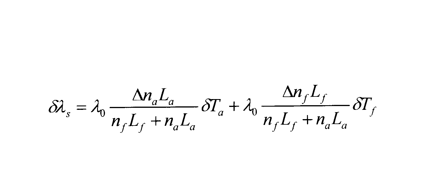
また、グレーティング反射波長の変化δλGは、下式で表される。 Here, λ0 represents the grating reflection wavelength in the initial state.
Further, the change ΔλG in the grating reflection wavelength is expressed by the following equation.

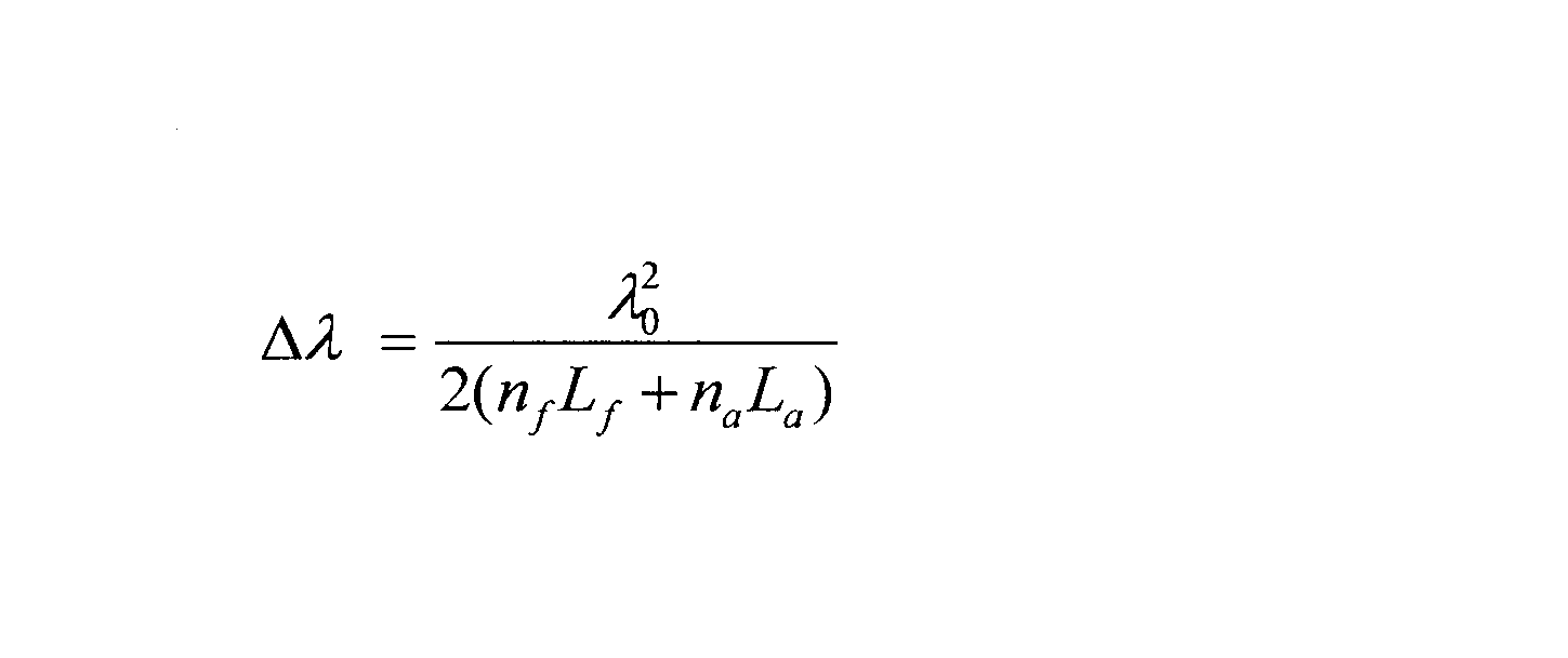
The longitudinal mode interval Δλ is approximately expressed by the following equation.

From
とグレーティング層の屈折率変化は一致させることができないので、モードホップが生じてしまう。 In order to suppress the mode hop, it is necessary to use the temperature within ΔTall or less, and the temperature is controlled by a Peltier device. In
する層を付加させている。このため共振器構造が、さらに大きくなるという問題がある。 In
前記光源が、前記半導体レーザ光を発振する活性層を備えており、
前記グレーティング素子が、前記半導体レーザ光が入射する入射面と所望波長の出射光を出射する出射面を有する光導波路、この光導波路内に形成されたブラッググレーティング、および前記入射面と前記ブラッググレーティングとの間に設けられている伝搬部を備えており、下記式(1)~式(5)の関係が満足されることを特徴とする。
ΔλG ≧0.8nm ・・・(1)
Lb ≦500μm ・・・(2)
La ≦500μm ・・・(3)
nb ≧1.8 ・・・(4)

式(2)において、Lbは、前記ブラッググレーティングの長さである。
式(3)において、Laは、前記活性層の長さである。
式(4)において、nbは、前記ブラッググレーティングを構成する材質の屈折率である。
式(5)において、dλG/dTは、ブラッグ波長の温度係数であり、dλTM/dTは、外部共振器レーザの位相条件を満足する波長の温度係数である。) The present invention is an external resonator type light emitting device that includes a light source that oscillates a semiconductor laser light alone, and a grating element that constitutes the light source and an external resonator, and oscillates in a single mode,
The light source includes an active layer that oscillates the semiconductor laser light;
The grating element includes an optical waveguide having an incident surface on which the semiconductor laser light is incident and an output surface that emits outgoing light of a desired wavelength, a Bragg grating formed in the optical waveguide, and the incident surface and the Bragg grating. Is provided, and the following equations (1) to (5) are satisfied.
Δλ G ≧ 0.8 nm (1)
L b ≦ 500 μm (2)
L a ≦ 500 μm (3)
n b ≧ 1.8 (4)
In Expression (2), L b is the length of the Bragg grating.
In the formula (3), L a is the length of the active layer.
In the formula (4), n b is the refractive index of the material constituting the Bragg grating.
In equation (5), dλ G / dT is the temperature coefficient of the Bragg wavelength, and dλ TM / dT is the temperature coefficient of the wavelength that satisfies the phase condition of the external cavity laser. )
きる。 For this reason, in the present invention, a material having a refractive index of 1.8 or more of the waveguide substrate on which the grating is formed is used. As a result, the temperature coefficient of the refractive index can be increased and dλ G / dT can be increased. Therefore, | dλ G / dT−dλ TM / dT | can be decreased, and the temperature range ΔT in which the mode hop occurs can be increased.
LWG ≦600μm ・・・(6)
1μm ≦Lg ≦10μm ・・(7)
20μm≦Lm ≦100μm ・・(8)
(式(6)において、LWGは、前記グレーティング素子の長さである。
式(7)において、Lgは、前記光源の出射面と前記光導波路の前記入射面との距離である。
式(8)において、Lmは、前記伝搬部の長さである。) In a preferred embodiment, the relationships of the following formulas (6) to (8) are satisfied.
L WG ≦ 600 μm (6)
1 μm ≦ L g ≦ 10 μm (7)
20 μm ≦ L m ≦ 100 μm (8)
(In Formula (6), LWG is the length of the grating element.
In Expression (7), L g is the distance between the exit surface of the light source and the entrance surface of the optical waveguide.
In Expression (8), L m is the length of the propagation unit. )
ここで、光源2は、単独でレーザ発振可能な光源とする。これは、光源2が、グレーティング素子がなくても、それ自体でレーザ発振することを意味する。 The
Here, the
基体4の外側端面には高反射膜6が設けられており、グレーティング素子側の端面には反射膜7Aが形成されている。 The
A
また、光学材料層の厚さは0.5~3.0μmであることが更に好ましい。 Further, the
The thickness of the optical material layer is more preferably 0.5 to 3.0 μm.
ただし、数式は抽象的で理解しにくいので、最初に、従来技術の典型的な形態と本発明の実施形態とを端的に比較し、本発明の特徴を述べる。次いで、本発明の各条件について述べていくこととする。 Hereinafter, the meaning of the conditions of the expressions (1) to (8) will be further described.
However, since the mathematical expressions are abstract and difficult to understand, first, typical features of the prior art and embodiments of the present invention will be compared briefly to describe the features of the present invention. Next, each condition of the present invention will be described.

First, the oscillation condition of the semiconductor laser is determined by gain condition × phase condition as shown in the following equation.
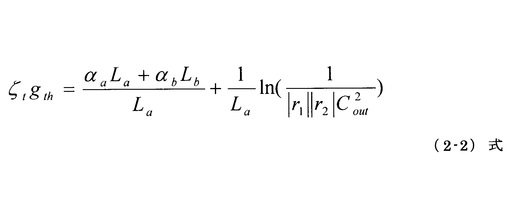
The gain condition is given by the following equation from equation (2-1).
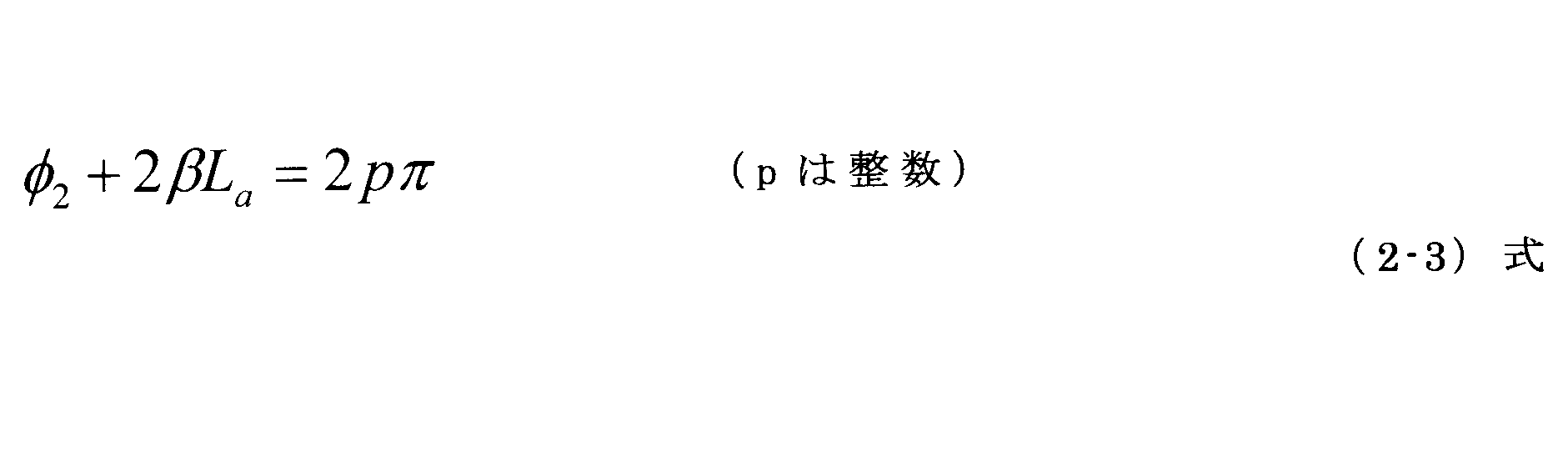
On the other hand, the phase condition is expressed by the following equation from the equation (2-1). However, φ1 is zero.
しかし、位相条件を満足する波長の温度依存性は、これに比してdλs/dT=dλTM/dT =0.05nm/℃と大きく、その差は0.04nm/℃となる。 In the case of a glass waveguide or FBG, the temperature dependence of λg is very small, and dλ G / dT = about 0.01 nm / ° C. For this reason, the external cavity laser has a feature of high wavelength stability.
However, the temperature dependence of the wavelength satisfying the phase condition is as large as dλ s / dT = dλ TM /dT=0.05 nm / ° C., and the difference is 0.04 nm / ° C.
ΔGTMは、外部共振器レーザの位相条件を満足する波長間隔(縦モード間隔)である。
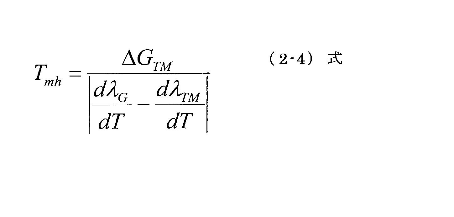
In general, the temperature T mh at which the mode hop occurs can be considered as the following equation from Non-Patent Document 1 (considered as Ta = Tf).
ΔG TM is a wavelength interval (longitudinal mode interval) that satisfies the phase condition of the external cavity laser.
本願は、グレーティング波長の温度係数と縦モードの温度係数を近づけることで温度無依存を実現するもので、このために共振器構造をコンパクトにでき、かつ付加するものが不要である。特許文献6では、各パラメータは以下のように記載されており、いずれも従来技術の範疇となっている。
△λG=0.4nm
縦モード間隔△GTM=0.2nm
グレーティング長Lb=3mm
LD活性層長さLa=600μm
伝搬部の長さ=1.5mm
In addition, it supplements also about the difference with
The present application realizes temperature independence by bringing the temperature coefficient of the grating wavelength and the temperature coefficient of the longitudinal mode close to each other. For this reason, the resonator structure can be made compact and an additional one is unnecessary. In
△ λ G = 0.4nm
Vertical mode interval △ G TM = 0.2nm
Grating length Lb = 3mm
LD active layer length La = 600μm
Propagation length = 1.5mm
ブラッグ反射率のピークにおける半値全幅ΔλGを0.8nm以上とする(式1)。λGはブラッグ波長である。すなわち、図5、図6、図7に示すように、横軸にブラッググレーティングによる反射波長をとり、縦軸に反射率をとったとき、反射率が最大となる波
長をブラッグ波長とする。またブラッグ波長を中心とするピークにおいて、反射率がピークの半分になる二つの波長の差を半値全幅ΔλGとする。 Hereinafter, each condition of the present invention will be further described.
The full width at half maximum Δλ G at the peak of the Bragg reflectance is set to 0.8 nm or more (Formula 1). λ G is the Bragg wavelength. That is, as shown in FIGS. 5, 6, and 7, when the reflection wavelength by the Bragg grating is taken on the horizontal axis and the reflectance is taken on the vertical axis, the wavelength at which the reflectance is maximized is the Bragg wavelength. In peak centered at the Bragg wavelength, the difference between the two wavelengths at which the reflectance becomes half the peak full width at half maximum [Delta] [lambda] G.
式(5)において、dλG/dTは、ブラッグ波長の温度係数である。
また、dλTM/dTは、外部共振器レーザの位相条件を満足する波長の温度係数である。 In addition, the condition shown in Formula (5) is important.
In equation (5), dλ G / dT is the temperature coefficient of the Bragg wavelength.
Dλ TM / dT is a temperature coefficient of the wavelength that satisfies the phase condition of the external cavity laser.
(2.3)式は、φ2+2βLa=2pπ、かつ、β=2π/λなので、これを満足するλがλTMとなる。φ2は、ブラッググレーティングの位相変化であり、下式で算出する。 The following supplements the vertical mode.
Since (2.3) is φ2 + 2βLa = 2pπ and β = 2π / λ, λ satisfying this is λ TM . φ2 is the phase change of the Bragg grating and is calculated by the following equation.
λTMは、複数存在するので、複数のλTMの差を意味する。先に用いた△λは△GTMに等しく、λsはλTMに等しい。 ΔG TM is a wavelength interval (longitudinal mode interval) that satisfies the phase condition of the external cavity laser.
lambda TM Since the plurality of, means the difference of a plurality of lambda TM. Previously used △ lambda equals △ G TM, λ s is equal to lambda TM.
伝搬部の長さLmは、20μm以上、100μm以下とする(式8)。これによって安定した発振が可能となる。 Distance L g between the exit surface and entrance surface of the optical waveguide of the light source, 1 [mu] m or more and 10μm or less (formula (7)). As a result, stable oscillation is possible.
The length L m of the propagation unit, 20 [mu] m or more and 100μm or less (equation 8). As a result, stable oscillation is possible.
なことから本願では、出射側の終点で共振器の長さを定義している。本発明によれば、非常に短い共振器長であっても、高い効率で目的波長の光を発振させることができる。この観点からは、活性層の外側端面とブラッググレーティングの出射側終点との間の長さが800μm以下であることが更に好ましく、700μm以下であることが特に好ましい。また、レーザの出力を高めるという観点からこの長さは、300μm以上であることが好ましい。 In a preferred embodiment, the light source and the grating element are directly optically connected, and a resonator structure is formed between the outer end surface opposite to the emission surface of the active layer and the Bragg grating, and the active layer The length between the outer end face of the light source and the exit end point of the Bragg grating is 900 μm or less. Since light is gradually reflected at the grating portion, it is not possible to observe a clear reflection point like a reflection mirror. Although the effective reflection point can be defined mathematically, it exists on the laser side from the end point on the emission side of the Bragg grating. For this reason, in the present application, the length of the resonator is defined at the end point on the emission side. According to the present invention, even with a very short resonator length, light of a target wavelength can be oscillated with high efficiency. From this viewpoint, the length between the outer end face of the active layer and the exit end point of the Bragg grating is more preferably 800 μm or less, and particularly preferably 700 μm or less. From the viewpoint of increasing the laser output, this length is preferably 300 μm or more.
図11(a)のグレーティング素子21Aでは、支持基板10上にバッファ層16が形成されており、バッファ層16上に光導波路30が形成されている。光導波路30は、前述したような屈折率1.8以上の光学材料からなるコアからなる。光導波路の横断面(光伝搬方向と垂直な方向の断面)形状は台形であり、光導波路は細長く伸びている。本例では、光導波路30の上側面が下側面よりも狭くなっている。光導波路30内には、前述したような入射側伝搬部、ブラッググレーティング、出射側伝搬部が形成されている。 11 and 12 relate to this embodiment.
In the grating element 21 </ b> A of FIG. 11A, the
なお、光導波路の幅Wmは、光導波路の横断面における幅のうち最も狭い部分の幅とする。 In the grating element 21 </ b> E of FIG. 10E, the
The width Wm of the optical waveguide is the width of the narrowest portion of the width in the cross section of the optical waveguide.
図1~図3に示すような装置を作製した。
具体的には、z板MgOドープのニオブ酸リチウム結晶基板にTiを成膜して、フォトリソグラフィー技術によりy軸方向にグレーティングパターンを作製した。その後、Tiパターンをマスクにしてフッ素系の反応性イオンエッチングにより、ピッチ間隔Λ180nm、長さLb100μmのグレーティング溝を形成した。グレーティングの溝深さは300nmであった。また、y軸伝搬の光導波路を形成するために、エキシマレーザにて、グレーティング部に、幅Wm3μm、Tr0.5μmの溝加工を実施した。さらに、溝形成面にSiO2からなるバッファ層17をスパッタ装置で0.5μm成膜し、支持基板としてブラックLN基板を使用してグレーティング形成面を接着した。 (Example 1)
An apparatus as shown in FIGS. 1 to 3 was produced.
Specifically, Ti was deposited on a z-plate MgO-doped lithium niobate crystal substrate, and a grating pattern was produced in the y-axis direction by photolithography. Thereafter, a grating groove having a pitch interval of Λ180 nm and a length of Lb of 100 μm was formed by fluorine-based reactive ion etching using the Ti pattern as a mask. The groove depth of the grating was 300 nm. In order to form an optical waveguide for y-axis propagation, an excimer laser was used to form a groove with a width of
光源素子仕様:
中心波長: 800nm
レーザ素子長 250μm
実装仕様:
Lg: 3μm
Lm: 20μm Next, a laser module was mounted as shown in FIG. 1 in order to evaluate the characteristics of an external resonator type laser using this grating element. A light source element having a GaAs laser structure, a highly reflective film on one end face, and an AR coat having a reflectance of 0.1% on the other end face was prepared.
Light source element specifications:
Center wavelength: 800nm
Laser element length 250μm
Mounting specifications:
Lg: 3μm
Lm: 20μm
実施例1と同様に、z板MgOドープのニオブ酸リチウム結晶基板にTiを成膜して、フォトリソグラフィー技術によりy軸方向にグレーティングパターンを作製した。その後、Tiパターンをマスクにしてフッ素系の反応性イオンエッチングによりピッチ間隔Λ180nm、長さLb1000μmのグレーティング溝を形成した。グレーティングの溝深さは300nmであった。また、y軸伝搬の光導波路を形成するためにエキシマレーザにてグレーティング部に幅Wm3μm、Tr 0.5μmの溝加工を実施した。 (Comparative Example 1)
Similarly to Example 1, Ti was deposited on a z-plate MgO-doped lithium niobate crystal substrate, and a grating pattern was produced in the y-axis direction by photolithography. Thereafter, a grating groove having a pitch interval of Λ180 nm and a length of Lb of 1000 μm was formed by fluorine reactive ion etching using the Ti pattern as a mask. The groove depth of the grating was 300 nm. Further, in order to form an optical waveguide for y-axis propagation, a groove with a width of
光源素子仕様:
中心波長: 800nm
レーザ素子長: 1000μm
実装仕様:
Lg: 3μm
Lm: 20μm Next, in order to evaluate the characteristics of the external resonator type laser using this grating element, a laser module as shown in another figure was mounted. A light source element having a GaAs laser structure, a highly reflective film on one end face, and an AR coat having a reflectance of 0.1% on the other end face was prepared.
Light source element specifications:
Center wavelength: 800nm
Laser element length: 1000μm
Mounting specifications:
Lg: 3μm
Lm: 20μm
図1および図4に示すような装置を作製した。
具体的には、z板MgOドープのニオブ酸リチウム結晶基板にTiを成膜して、フォトリソグラフィー技術によりy軸方向にグレーティングパターンを作製した。その後、Tiパターンをマスクにしてフッ素系の反応性イオンエッチングにより、ピッチ間隔Λ214nm、長さLb 100μmのグレーティング溝を形成した。グレーティングの溝深さは40nmであった。また、y軸伝搬の光導波路を形成するために、エキシマレーザにて、グレーティング部に、幅Wm3μm、Tr0.5μmの溝加工を実施した。さらに、溝形成面にSiO2からなるバッファ層17をスパッタ装置で0.5μm成膜し、支持基板としてブラックLN基板を使用してグレーティング形成面を接着した。ブラックLNとは、酸素欠損状態にしたニオブ酸リチウムのことであり、焦電による電荷発生を抑制できる。これにより温度変動があった場合の耐サージによる基板クラックを防止できる。 (Example 2)
An apparatus as shown in FIGS. 1 and 4 was produced.
Specifically, Ti was deposited on a z-plate MgO-doped lithium niobate crystal substrate, and a grating pattern was produced in the y-axis direction by photolithography. Thereafter, a grating groove having a pitch interval of Λ214 nm and a length of Lb of 100 μm was formed by fluorine-based reactive ion etching using the Ti pattern as a mask. The groove depth of the grating was 40 nm. In order to form an optical waveguide for y-axis propagation, an excimer laser was used to form a groove with a width of
光源素子仕様:
中心波長: 950nm
出力 20mW
半値幅: 50nm
レーザ素子長 250μm
実装仕様:
Lg: 1μm
Lm: 20μm Next, a laser module was mounted as shown in FIG. 1 in order to evaluate the characteristics of an external resonator type laser using this grating element. A light source element having a GaAs laser structure, a highly reflective film on one end face, and an AR coat having a reflectance of 0.1% on the other end face was prepared.
Light source element specifications:
Center wavelength: 950nm
Output 20mW
Half width: 50nm
Laser element length 250μm
Mounting specifications:
Lg: 1μm
Lm: 20μm
実施例2と同じ方法で、ピッチ間隔Λ222nm、長さLb 100μmのグレーティング溝を形成した。グレーティングの溝深さは40nmとした。グレーティング素子の光学特性は、広帯域波長光源であるスーパ・ルミネッセンス・ダイオード(SLD)を使用して、グレーティング素子に光を入力して出力光を光スペクトルアナライザで分析することにより、その透過特性から反射特性を評価した。その結果、TEモードに対して中心波長975nm、最大反射率は20%で、半値全幅△λGは2nmの特性を得た。 (Example 3)
A grating groove having a pitch interval of Λ222 nm and a length of Lb of 100 μm was formed in the same manner as in Example 2. The grating groove depth was 40 nm. Optical characteristics of the grating element are reflected from its transmission characteristics by using a super luminescence diode (SLD), which is a broadband wavelength light source, and inputting light into the grating element and analyzing the output light with an optical spectrum analyzer. Characteristics were evaluated. As a result, with respect to the TE mode, a center wavelength of 975 nm, a maximum reflectance of 20%, and a full width at half maximum Δλ G of 2 nm were obtained.
光源素子仕様:
中心波長: 977nm
出力: 50mW
半値幅: 0.1nm
レーザ素子長 250μm
実装仕様:
Lg: 1μm
Lm: 20μm Next, a laser module was mounted as shown in FIG. The light source element was a normal GaAs laser, and the exit end face was not coated with AR.
Light source element specifications:
Center wavelength: 977nm
Output: 50mW
Half width: 0.1nm
Laser element length 250μm
Mounting specifications:
Lg: 1μm
Lm: 20μm
実施例3において、グレーティング素子がない場合には、レーザ発振波長の温度係数は0.3nm/℃で大きく、モードホップ温度は10℃程度とであった。10℃以上ではパワー変動が大きくなり、出力変動は10%以上となった。 (Comparative Example 2)
In Example 3, when there was no grating element, the temperature coefficient of the laser oscillation wavelength was large at 0.3 nm / ° C., and the mode hop temperature was about 10 ° C. At 10 ° C or higher, the power fluctuation became large, and the output fluctuation became 10% or more.
石英基板にスパッタ装置にてTa2O5を1.2μm成膜して光学材料層を形成した。次に、Ta2O5上にTiを成膜して、フォトリソグラフィー技術によりy軸方向にグレーティングパターンを作製した。その後、Tiパターンをマスクにしてフッ素系の反応性イオンエッチングにより、ピッチ間隔Λ232nm、長さLb 100μmのグレーティング溝を形成した。グレーティングの溝深さは40nmとした。次に、上記と同様にして反応性イオンエッチングにより、明細書図2、3に示す形状の光導波路を形成した。グレーティング素子の光学特性は、広帯域波長光源であるスーパ・ルミネッセンス・ダイオード(SLD)を使用して、グレーティング素子に光を入力して出力光を光スペクトルアナライザで分析することにより、その透過特性から反射特性を評価した。その結果、TEモードに対して中心波長945nm、最大反射率は20%で、半値全幅△λGは2nmの特性を得た。 Example 4
An optical material layer was formed on a quartz substrate by depositing Ta2O5 with a thickness of 1.2 μm using a sputtering apparatus. Next, Ti was deposited on Ta2O5, and a grating pattern was produced in the y-axis direction by photolithography. Thereafter, a grating groove having a pitch interval of Λ232 nm and a length of Lb of 100 μm was formed by fluorine reactive ion etching using the Ti pattern as a mask. The grating groove depth was 40 nm. Next, an optical waveguide having the shape shown in FIGS. 2 and 3 was formed by reactive ion etching in the same manner as described above. Optical characteristics of the grating element are reflected from its transmission characteristics by using a super luminescence diode (SLD), which is a broadband wavelength light source, and inputting light into the grating element and analyzing the output light with an optical spectrum analyzer. Characteristics were evaluated. As a result, a characteristic with a center wavelength of 945 nm, a maximum reflectance of 20%, and a full width at half maximum Δλ G of 2 nm with respect to the TE mode was obtained.
光源素子仕様:
中心波長: 950nm
出力: 20mW
半値幅: 50nm
レーザ素子長 250μm
実装仕様:
Lg: 1μm
Lm: 20μm Next, a laser module was mounted as shown in FIG. The light source element was a normal GaAs laser, and a 0.1% AR coat was formed on the emission end face.
Light source element specifications:
Center wavelength: 950nm
Output: 20mW
Half width: 50nm
Laser element length 250μm
Mounting specifications:
Lg: 1μm
Lm: 20μm
実施例1と同様にして、図1、図3に示すような装置を作製した。ただし、グレーティング素子21Dの横断面形状は、図12(a)に示す形状とした。 (Example 5)
In the same manner as in Example 1, devices as shown in FIGS. 1 and 3 were produced. However, the cross-sectional shape of the
次に、Ta2O5上にTiを成膜して、EB描画装置によりグレーティングパターンを作製した。その後、Tiパターンをマスクにしてフッ素系の反応性イオンエッチングにより、ピッチ間隔Λ238.5nm、長さLb 100μmのブラッググレーティングを形成した。グレーティングの溝深さtdは40nmとした。 Specifically, a SiO 2 layer 16 that is a lower clad layer is formed on a
Next, a film of Ti was formed on Ta2O5, and a grating pattern was produced by an EB drawing apparatus. Thereafter, a Bragg grating having a pitch interval of Λ238.5 nm and a length of Lb of 100 μm was formed by fluorine-based reactive ion etching using the Ti pattern as a mask. The groove depth td of the grating was 40 nm.
最後に、上側クラッドとなるSiO2からなるバッファ層23を光導波路30を覆うように2μmスパッタにて形成した。 Further, in order to form the
Finally, a
光源素子仕様:
中心波長: 977nm
出力: 50mW
半値幅: 0.1nm
レーザ素子長 250μm
実装仕様:
Lg: 1μm
Lm: 20μm Next, a laser module was mounted as shown in FIG. The light source element was a normal GaAs laser, and the exit end face was not coated with AR.
Light source element specifications:
Center wavelength: 977nm
Output: 50mW
Half width: 0.1nm
Laser element length 250μm
Mounting specifications:
Lg: 1μm
Lm: 20μm
After mounting the module, when driven by current control (ACC) without using a Peltier element, it oscillates at a center wavelength of 975 nm corresponding to the reflection wavelength of the grating, and the output is smaller than that without the grating element, but a 40 mW laser It was a characteristic. In addition, in order to evaluate the operating temperature range, a module was installed in a thermostat and the temperature dependence of the laser oscillation wavelength and output fluctuation were measured. As a result, the temperature coefficient of the oscillation wavelength was 0.03 nm / ° C., the temperature range where the output fluctuation due to the mode hop was large was 40 ° C., and the power output fluctuation within this temperature range was within 1% even when the mode hop occurred.
Claims (8)
- 単独で半導体レーザ光を発振する光源、およびこの光源と外部共振器を構成するグレーティング素子を備え、単一モード発振する外部共振器型発光装置であって、
前記光源が、前記半導体レーザ光を発振する活性層を備えており、
前記グレーティング素子が、前記半導体レーザ光が入射する入射面と所望波長の出射光を出射する出射面を有する光導波路、この光導波路内に形成されたブラッググレーティング、および前記入射面と前記ブラッググレーティングとの間に設けられている伝搬部を備えており、下記式(1)~式(5)の関係が満足されることを特徴とする、外部共振器型発光装置。
ΔλG ≧0.8nm ・・・(1)
Lb ≦500μm ・・・(2)
La ≦500μm ・・・(3)
nb ≧1.8 ・・・(4)

式(2)において、Lbは、前記ブラッググレーティングの長さである。
式(3)において、Laは、前記活性層の長さである。
式(4)において、nbは、前記ブラッググレーティングを構成する材質の屈折率である。
式(5)において、dλG/dTは、ブラッグ波長の温度係数であり、dλTM/dTは、外部共振器レーザの位相条件を満足する波長の温度係数である。)
A light source that independently oscillates semiconductor laser light, and a grating element that constitutes the light source and an external resonator, and an external resonator type light emitting device that oscillates in a single mode
The light source includes an active layer that oscillates the semiconductor laser light;
The grating element includes an optical waveguide having an incident surface on which the semiconductor laser light is incident and an output surface that emits outgoing light of a desired wavelength, a Bragg grating formed in the optical waveguide, and the incident surface and the Bragg grating. An external resonator type light emitting device characterized by satisfying the following formulas (1) to (5).
Δλ G ≧ 0.8 nm (1)
L b ≦ 500 μm (2)
L a ≦ 500 μm (3)
n b ≧ 1.8 (4)
In Expression (2), L b is the length of the Bragg grating.
In the formula (3), L a is the length of the active layer.
In the formula (4), n b is the refractive index of the material constituting the Bragg grating.
In equation (5), dλ G / dT is the temperature coefficient of the Bragg wavelength, and dλ TM / dT is the temperature coefficient of the wavelength that satisfies the phase condition of the external cavity laser. )
- 前記光源と前記グレーティング素子が直接光学的に接続されており、前記活性層の出射面と反対側の外側端面と前記ブラッググレーティングとの間で前記外部共振器を形成しており、前記活性層の前記外側端面と前記ブラッググレーティングの出射側終点との間の長
さが910μm以下であることを特徴とする、請求項1記載の装置。
The light source and the grating element are directly optically connected, and the external resonator is formed between the outer end surface opposite to the emission surface of the active layer and the Bragg grating, and the active layer The apparatus according to claim 1, wherein a length between the outer end face and an exit end point of the Bragg grating is 910 μm or less.
- 下記式(6)~(8)の関係が満足されることを特徴とする、請求項1または2記載の装置。
LWG ≦600μm ・・・(6)
1μm ≦Lg ≦10μm ・・(7)
20μm≦Lm ≦100μm ・・(8)
(式(6)において、LWGは、前記グレーティング素子の長さである。
式(7)において、Lgは、前記光源の出射面と前記光導波路の前記入射面との距離である。
式(8)において、Lmは、前記伝搬部の長さである。) The apparatus according to claim 1 or 2, wherein a relationship of the following formulas (6) to (8) is satisfied.
L WG ≦ 600 μm (6)
1 μm ≦ L g ≦ 10 μm (7)
20 μm ≦ L m ≦ 100 μm (8)
(In Formula (6), LWG is the length of the grating element.
In Expression (7), L g is the distance between the exit surface of the light source and the entrance surface of the optical waveguide.
In Expression (8), L m is the length of the propagation unit. ) - 前記ブラッググレーティングの反射率が、前記光源の出射端の反射率、前記グレーティング素子の入射面の反射率、および前記グレーティング素子の出射面の反射率よりも大きいことを特徴とする、請求項1~3のいずれか一つの請求項に記載の装置。 The reflectance of the Bragg grating is larger than the reflectance of the exit end of the light source, the reflectance of the entrance surface of the grating element, and the reflectance of the exit surface of the grating element. 4. An apparatus according to any one of claims 3.
- 前記光導波路が細長いコアからなり、前記コアの横断面が凸図形をなしていることを特徴とする、請求項1~4のいずれか一つの請求項に記載の装置。 The apparatus according to any one of claims 1 to 4, wherein the optical waveguide comprises an elongated core, and a cross section of the core has a convex shape.
- 前記光導波路が、リッジ部と、このリッジ部を成形する少なくとも一対のリッジ溝からなることを特徴とする、請求項1~4のいずれか一つの請求項に記載の装置。 The apparatus according to any one of claims 1 to 4, wherein the optical waveguide includes a ridge portion and at least a pair of ridge grooves forming the ridge portion.
- 前記ブラッググレーティングの前記材質が、ガリウム砒素、ニオブ酸リチウム単結晶、酸化タンタル、酸化亜鉛および酸化アルミナからなる群より選択されることを特徴とする、請求項1~6のいずれか一つの請求項に記載の装置。 The material according to any one of claims 1 to 6, wherein the material of the Bragg grating is selected from the group consisting of gallium arsenide, lithium niobate single crystal, tantalum oxide, zinc oxide, and alumina oxide. The device described in 1.
- 前記光導波路上に設けられたバッファ層を有することを特徴とする、請求項1~7のいずれか一つの請求項に記載の装置。
The device according to any one of claims 1 to 7, further comprising a buffer layer provided on the optical waveguide.
Priority Applications (4)
| Application Number | Priority Date | Filing Date | Title |
|---|---|---|---|
| JP2015514679A JP5936771B2 (en) | 2013-11-27 | 2014-11-17 | External resonator type light emitting device |
| EP14865296.9A EP3076500B1 (en) | 2013-11-27 | 2014-11-17 | External-resonator-type light emitting device |
| CN201480063207.1A CN105765802B (en) | 2013-11-27 | 2014-11-17 | External resonator type light emitting device |
| US15/165,004 US10063034B2 (en) | 2013-11-27 | 2016-05-26 | External resonator-type light emitting device |
Applications Claiming Priority (4)
| Application Number | Priority Date | Filing Date | Title |
|---|---|---|---|
| JP2013244747 | 2013-11-27 | ||
| JP2013-244747 | 2013-11-27 | ||
| JP2014115389 | 2014-06-04 | ||
| JP2014-115389 | 2014-06-04 |
Related Child Applications (1)
| Application Number | Title | Priority Date | Filing Date |
|---|---|---|---|
| US15/165,004 Continuation US10063034B2 (en) | 2013-11-27 | 2016-05-26 | External resonator-type light emitting device |
Publications (1)
| Publication Number | Publication Date |
|---|---|
| WO2015079939A1 true WO2015079939A1 (en) | 2015-06-04 |
Family
ID=53198885
Family Applications (1)
| Application Number | Title | Priority Date | Filing Date |
|---|---|---|---|
| PCT/JP2014/080301 WO2015079939A1 (en) | 2013-11-27 | 2014-11-17 | External-resonator-type light emitting device |
Country Status (5)
| Country | Link |
|---|---|
| US (1) | US10063034B2 (en) |
| EP (1) | EP3076500B1 (en) |
| JP (1) | JP5936771B2 (en) |
| CN (1) | CN105765802B (en) |
| WO (1) | WO2015079939A1 (en) |
Cited By (4)
| Publication number | Priority date | Publication date | Assignee | Title |
|---|---|---|---|---|
| US9331454B2 (en) | 2013-11-27 | 2016-05-03 | Ngk Insulators, Ltd. | External resonator type light emitting system |
| US9627853B2 (en) | 2013-06-07 | 2017-04-18 | Ngk Insulators, Ltd. | External resonator-type light emitting device |
| US10063034B2 (en) | 2013-11-27 | 2018-08-28 | Ngk Insulators, Ltd. | External resonator-type light emitting device |
| JPWO2018100868A1 (en) * | 2016-12-02 | 2019-10-17 | 日本碍子株式会社 | Optical element and manufacturing method thereof |
Families Citing this family (4)
| Publication number | Priority date | Publication date | Assignee | Title |
|---|---|---|---|---|
| WO2015190569A1 (en) * | 2014-06-13 | 2015-12-17 | 日本碍子株式会社 | External-resonator-type light-emission device |
| WO2020003118A1 (en) * | 2018-06-29 | 2020-01-02 | 3M Innovative Properties Company | Optical waveguide with spatially modulated index region |
| JP7239920B2 (en) * | 2019-03-01 | 2023-03-15 | 富士フイルムビジネスイノベーション株式会社 | Semiconductor optical amplifier, semiconductor optical amplifier, optical output device, and distance measuring device |
| CN110380326B (en) * | 2019-07-29 | 2020-10-23 | 武汉电信器件有限公司 | Optical signal output device and method, and storage medium |
Citations (15)
| Publication number | Priority date | Publication date | Assignee | Title |
|---|---|---|---|---|
| JPS56148880A (en) | 1980-04-21 | 1981-11-18 | Nec Corp | Single longitudinal mode semiconductor laser |
| JPH0560927A (en) * | 1991-09-02 | 1993-03-12 | Shimadzu Corp | Optical waveguide |
| JPH09128689A (en) | 1995-11-01 | 1997-05-16 | Yoshiaki Masuno | Car navigation device |
| JPH1098230A (en) * | 1996-09-25 | 1998-04-14 | Nippon Telegr & Teleph Corp <Ntt> | Frequency stabilized laser |
| JP2000082864A (en) | 1998-09-04 | 2000-03-21 | Nippon Telegr & Teleph Corp <Ntt> | Laser device |
| JP2002050827A (en) * | 2000-08-01 | 2002-02-15 | Sumitomo Electric Ind Ltd | Semiconductor laser |
| JP2002134833A (en) | 2000-10-23 | 2002-05-10 | Nippon Telegr & Teleph Corp <Ntt> | Temperature independent laser |
| JP2003110193A (en) * | 2001-08-06 | 2003-04-11 | Nanoplus Gmbh Nanosystems & Technologies | Semiconductor laser with weakly coupled grating |
| US20040020893A1 (en) * | 2002-01-17 | 2004-02-05 | Bookham Technology, Plc. | Method of producing a rib waveguide |
| JP2006222399A (en) | 2005-02-14 | 2006-08-24 | Hamamatsu Photonics Kk | Semiconductor laser device |
| US20070127538A1 (en) * | 2005-12-07 | 2007-06-07 | Electronics And Telecommunications Research Institute | Athermal external cavity laser |
| JP2010171252A (en) | 2009-01-23 | 2010-08-05 | Fujitsu Ltd | Optical transmission device |
| US20120099611A1 (en) * | 2009-06-12 | 2012-04-26 | Mel | External cavity tunable laser module |
| WO2013034813A2 (en) | 2011-09-07 | 2013-03-14 | Epicrystals Oy | Wavelength conversion unit |
| JP5641631B1 (en) * | 2014-06-04 | 2014-12-17 | 日本碍子株式会社 | External resonator type light emitting device |
Family Cites Families (35)
| Publication number | Priority date | Publication date | Assignee | Title |
|---|---|---|---|---|
| JPS49128689A (en) | 1973-04-06 | 1974-12-10 | ||
| JPH01201983A (en) * | 1988-02-05 | 1989-08-14 | Nippon Telegr & Teleph Corp <Ntt> | Semiconductor laser device |
| US5185752A (en) * | 1992-02-18 | 1993-02-09 | Spectra Diode Laboratories, Inc. | Coupling arrangements for frequency-doubled diode lasers |
| US5418802A (en) * | 1993-11-12 | 1995-05-23 | Eastman Kodak Company | Frequency tunable waveguide extended cavity laser |
| EP0703649B1 (en) * | 1994-09-14 | 2003-01-15 | Matsushita Electric Industrial Co., Ltd. | Method for stabilizing output of higher harmonic waves and short wavelength laser beam source using the same |
| JP3526671B2 (en) * | 1995-08-25 | 2004-05-17 | アンリツ株式会社 | Laser light source device |
| US5870417A (en) * | 1996-12-20 | 1999-02-09 | Sdl, Inc. | Thermal compensators for waveguide DBR laser sources |
| JPH10221572A (en) | 1997-02-07 | 1998-08-21 | Fujitsu Ltd | Optical device |
| US5914972A (en) | 1997-03-24 | 1999-06-22 | Sdl, Inc. | Thermal compensators for waveguide DBR laser sources |
| JP3394445B2 (en) * | 1998-05-15 | 2003-04-07 | 日本電信電話株式会社 | Tunable semiconductor laser |
| EP1069659A4 (en) | 1999-02-03 | 2003-03-05 | Furukawa Electric Co Ltd | Semiconductor laser and semiconductor laser module using the same |
| FR2793077B1 (en) | 1999-04-30 | 2001-07-27 | Cit Alcatel | LASER WITH EXTENDED OPERATING TEMPERATURE RANGE |
| US6580734B1 (en) | 1999-07-07 | 2003-06-17 | Cyoptics Ltd. | Laser wavelength stabilization |
| EP1130710A3 (en) | 2000-01-20 | 2003-09-17 | Cyoptics (Israel) Ltd. | High repetition rate optical pulse generator |
| US6614822B2 (en) | 2000-02-03 | 2003-09-02 | The Furukawa Electric Co., Ltd. | Semiconductor laser devices, and semiconductor laser modules and optical communication systems using the same |
| JP2001257422A (en) | 2000-03-10 | 2001-09-21 | Sumitomo Electric Ind Ltd | Semiconductor laser module |
| JP2001272559A (en) * | 2000-03-27 | 2001-10-05 | Fuji Photo Film Co Ltd | Optical waveguide element and semiconductor laser device |
| JP2002374037A (en) * | 2001-02-02 | 2002-12-26 | Furukawa Electric Co Ltd:The | Semiconductor laser module, fiber-optic amplifier using the same and optical communication system |
| JP2002319738A (en) * | 2001-04-19 | 2002-10-31 | Furukawa Electric Co Ltd:The | Semiconductor laser device, semiconductor laser module and raman amplifier using the same |
| US6839377B2 (en) | 2001-10-26 | 2005-01-04 | Agere Systems, Inc. | Optoelectronic device having a fiber grating stabilized pump module with increased locking range and a method of manufacture therefor |
| JP4066738B2 (en) * | 2002-07-30 | 2008-03-26 | 株式会社島津製作所 | Laser equipment |
| US6819702B2 (en) | 2002-09-11 | 2004-11-16 | Bookham Technology Plc | Pump laser diode with improved wavelength stability |
| JP3729170B2 (en) | 2002-10-18 | 2005-12-21 | 住友電気工業株式会社 | Semiconductor laser |
| US6920159B2 (en) * | 2002-11-29 | 2005-07-19 | Optitune Plc | Tunable optical source |
| DE10303927B4 (en) | 2003-01-31 | 2005-03-31 | Fraunhofer-Gesellschaft zur Förderung der angewandten Forschung e.V. | Probe for a near field optical microscope with improved scattered light suppression and method for its production |
| DE10321986B4 (en) | 2003-05-15 | 2005-07-14 | Fraunhofer-Gesellschaft zur Förderung der angewandten Forschung e.V. | Apparatus and method for level correcting in a wave field synthesis system |
| KR100547897B1 (en) | 2003-06-30 | 2006-01-31 | 삼성전자주식회사 | Tunable Laser Device |
| WO2006109730A1 (en) * | 2005-04-07 | 2006-10-19 | Matsushita Electric Industrial Co., Ltd. | Laser light source and optical device |
| KR100772529B1 (en) * | 2006-04-20 | 2007-11-01 | 한국전자통신연구원 | Wavelength tunable external cavity laser |
| US8369203B2 (en) | 2010-02-25 | 2013-02-05 | Tdk Corporation | Thermally-assisted magnetic recording head having concave core at light entrance surface |
| JP2013140225A (en) * | 2011-12-28 | 2013-07-18 | Citizen Holdings Co Ltd | Laser light source |
| US9184564B2 (en) * | 2013-06-07 | 2015-11-10 | Ngk Insulators, Ltd. | External resonator type light emitting system |
| CN105765802B (en) | 2013-11-27 | 2020-01-07 | 日本碍子株式会社 | External resonator type light emitting device |
| WO2015079986A1 (en) * | 2013-11-27 | 2015-06-04 | 日本碍子株式会社 | Reflective optical sensor element |
| US9331454B2 (en) | 2013-11-27 | 2016-05-03 | Ngk Insulators, Ltd. | External resonator type light emitting system |
-
2014
- 2014-11-17 CN CN201480063207.1A patent/CN105765802B/en active Active
- 2014-11-17 EP EP14865296.9A patent/EP3076500B1/en active Active
- 2014-11-17 WO PCT/JP2014/080301 patent/WO2015079939A1/en active Application Filing
- 2014-11-17 JP JP2015514679A patent/JP5936771B2/en active Active
-
2016
- 2016-05-26 US US15/165,004 patent/US10063034B2/en active Active
Patent Citations (16)
| Publication number | Priority date | Publication date | Assignee | Title |
|---|---|---|---|---|
| JPS56148880A (en) | 1980-04-21 | 1981-11-18 | Nec Corp | Single longitudinal mode semiconductor laser |
| JPH0560927A (en) * | 1991-09-02 | 1993-03-12 | Shimadzu Corp | Optical waveguide |
| JPH09128689A (en) | 1995-11-01 | 1997-05-16 | Yoshiaki Masuno | Car navigation device |
| JPH1098230A (en) * | 1996-09-25 | 1998-04-14 | Nippon Telegr & Teleph Corp <Ntt> | Frequency stabilized laser |
| JP2000082864A (en) | 1998-09-04 | 2000-03-21 | Nippon Telegr & Teleph Corp <Ntt> | Laser device |
| JP3667209B2 (en) | 2000-08-01 | 2005-07-06 | 住友電気工業株式会社 | Semiconductor laser |
| JP2002050827A (en) * | 2000-08-01 | 2002-02-15 | Sumitomo Electric Ind Ltd | Semiconductor laser |
| JP2002134833A (en) | 2000-10-23 | 2002-05-10 | Nippon Telegr & Teleph Corp <Ntt> | Temperature independent laser |
| JP2003110193A (en) * | 2001-08-06 | 2003-04-11 | Nanoplus Gmbh Nanosystems & Technologies | Semiconductor laser with weakly coupled grating |
| US20040020893A1 (en) * | 2002-01-17 | 2004-02-05 | Bookham Technology, Plc. | Method of producing a rib waveguide |
| JP2006222399A (en) | 2005-02-14 | 2006-08-24 | Hamamatsu Photonics Kk | Semiconductor laser device |
| US20070127538A1 (en) * | 2005-12-07 | 2007-06-07 | Electronics And Telecommunications Research Institute | Athermal external cavity laser |
| JP2010171252A (en) | 2009-01-23 | 2010-08-05 | Fujitsu Ltd | Optical transmission device |
| US20120099611A1 (en) * | 2009-06-12 | 2012-04-26 | Mel | External cavity tunable laser module |
| WO2013034813A2 (en) | 2011-09-07 | 2013-03-14 | Epicrystals Oy | Wavelength conversion unit |
| JP5641631B1 (en) * | 2014-06-04 | 2014-12-17 | 日本碍子株式会社 | External resonator type light emitting device |
Non-Patent Citations (2)
| Title |
|---|
| TECHNICAL REPORTS ON FUNDAMENTALS OF ELECTRONICS, COMMUNICATIONS AND COMPUTER SCIENCES, vol. 105, no. 52, 2005, pages 17 - 20 |
| TRANSACTIONS ON FUNDAMENTALS OF ELECTRONICS, COMMUNICATIONS AND COMPUTER SCIENCES, vol. J81, no. 7, July 1998 (1998-07-01), pages 664 - 665 |
Cited By (5)
| Publication number | Priority date | Publication date | Assignee | Title |
|---|---|---|---|---|
| US9627853B2 (en) | 2013-06-07 | 2017-04-18 | Ngk Insulators, Ltd. | External resonator-type light emitting device |
| US9331454B2 (en) | 2013-11-27 | 2016-05-03 | Ngk Insulators, Ltd. | External resonator type light emitting system |
| US10063034B2 (en) | 2013-11-27 | 2018-08-28 | Ngk Insulators, Ltd. | External resonator-type light emitting device |
| JPWO2018100868A1 (en) * | 2016-12-02 | 2019-10-17 | 日本碍子株式会社 | Optical element and manufacturing method thereof |
| JP7061572B2 (en) | 2016-12-02 | 2022-04-28 | 日本碍子株式会社 | Optical element and its manufacturing method |
Also Published As
| Publication number | Publication date |
|---|---|
| CN105765802B (en) | 2020-01-07 |
| EP3076500A4 (en) | 2017-07-12 |
| JP5936771B2 (en) | 2016-06-22 |
| EP3076500B1 (en) | 2018-10-10 |
| JPWO2015079939A1 (en) | 2017-03-16 |
| EP3076500A1 (en) | 2016-10-05 |
| US10063034B2 (en) | 2018-08-28 |
| CN105765802A (en) | 2016-07-13 |
| US20160268773A1 (en) | 2016-09-15 |
Similar Documents
| Publication | Publication Date | Title |
|---|---|---|
| JP6125631B2 (en) | External resonator type light emitting device | |
| JP5936771B2 (en) | External resonator type light emitting device | |
| US9331454B2 (en) | External resonator type light emitting system | |
| JP6554035B2 (en) | Grating element and external resonator type light emitting device | |
| WO2015107960A1 (en) | External resonator type light emitting device | |
| JP5641631B1 (en) | External resonator type light emitting device | |
| JP6572209B2 (en) | Optical device and method for manufacturing optical device | |
| JP5936777B2 (en) | Grating element and external resonator type light emitting device | |
| WO2015190569A1 (en) | External-resonator-type light-emission device | |
| WO2016093187A1 (en) | External resonator type light-emitting device | |
| WO2015190385A1 (en) | External resonator-type light-emitting device | |
| JP2015039011A (en) | External resonator light-emitting device | |
| WO2015108197A1 (en) | External resonator type light emitting device | |
| WO2015087914A1 (en) | External-resonator-type light-emitting device | |
| JP2015115457A (en) | External resonator light-emitting device | |
| JP2015103732A (en) | Grating element and external resonator light-emitting device | |
| WO2017043222A1 (en) | Optical device | |
| WO2016125746A1 (en) | Optical waveguide element and optical device |
Legal Events
| Date | Code | Title | Description |
|---|---|---|---|
| ENP | Entry into the national phase |
Ref document number: 2015514679 Country of ref document: JP Kind code of ref document: A |
|
| 121 | Ep: the epo has been informed by wipo that ep was designated in this application |
Ref document number: 14865296 Country of ref document: EP Kind code of ref document: A1 |
|
| NENP | Non-entry into the national phase |
Ref country code: DE |
|
| REEP | Request for entry into the european phase |
Ref document number: 2014865296 Country of ref document: EP |
|
| WWE | Wipo information: entry into national phase |
Ref document number: 2014865296 Country of ref document: EP |