WO2015079913A1 - 発光装置用基板、発光装置および発光装置用基板の製造方法 - Google Patents
発光装置用基板、発光装置および発光装置用基板の製造方法 Download PDFInfo
- Publication number
- WO2015079913A1 WO2015079913A1 PCT/JP2014/079943 JP2014079943W WO2015079913A1 WO 2015079913 A1 WO2015079913 A1 WO 2015079913A1 JP 2014079943 W JP2014079943 W JP 2014079943W WO 2015079913 A1 WO2015079913 A1 WO 2015079913A1
- Authority
- WO
- WIPO (PCT)
- Prior art keywords
- substrate
- light emitting
- emitting device
- glass
- layer
- Prior art date
- Legal status (The legal status is an assumption and is not a legal conclusion. Google has not performed a legal analysis and makes no representation as to the accuracy of the status listed.)
- Ceased
Links
Images












Classifications
-
- H—ELECTRICITY
- H10—SEMICONDUCTOR DEVICES; ELECTRIC SOLID-STATE DEVICES NOT OTHERWISE PROVIDED FOR
- H10H—INORGANIC LIGHT-EMITTING SEMICONDUCTOR DEVICES HAVING POTENTIAL BARRIERS
- H10H20/00—Individual inorganic light-emitting semiconductor devices having potential barriers, e.g. light-emitting diodes [LED]
- H10H20/80—Constructional details
- H10H20/85—Packages
- H10H20/858—Means for heat extraction or cooling
- H10H20/8581—Means for heat extraction or cooling characterised by their material
-
- H—ELECTRICITY
- H10—SEMICONDUCTOR DEVICES; ELECTRIC SOLID-STATE DEVICES NOT OTHERWISE PROVIDED FOR
- H10H—INORGANIC LIGHT-EMITTING SEMICONDUCTOR DEVICES HAVING POTENTIAL BARRIERS
- H10H20/00—Individual inorganic light-emitting semiconductor devices having potential barriers, e.g. light-emitting diodes [LED]
- H10H20/80—Constructional details
- H10H20/84—Coatings, e.g. passivation layers or antireflective coatings
-
- H—ELECTRICITY
- H10—SEMICONDUCTOR DEVICES; ELECTRIC SOLID-STATE DEVICES NOT OTHERWISE PROVIDED FOR
- H10H—INORGANIC LIGHT-EMITTING SEMICONDUCTOR DEVICES HAVING POTENTIAL BARRIERS
- H10H20/00—Individual inorganic light-emitting semiconductor devices having potential barriers, e.g. light-emitting diodes [LED]
- H10H20/80—Constructional details
- H10H20/85—Packages
- H10H20/851—Wavelength conversion means
- H10H20/8511—Wavelength conversion means characterised by their material, e.g. binder
- H10H20/8512—Wavelength conversion materials
-
- H—ELECTRICITY
- H10—SEMICONDUCTOR DEVICES; ELECTRIC SOLID-STATE DEVICES NOT OTHERWISE PROVIDED FOR
- H10H—INORGANIC LIGHT-EMITTING SEMICONDUCTOR DEVICES HAVING POTENTIAL BARRIERS
- H10H20/00—Individual inorganic light-emitting semiconductor devices having potential barriers, e.g. light-emitting diodes [LED]
- H10H20/80—Constructional details
- H10H20/85—Packages
- H10H20/852—Encapsulations
- H10H20/854—Encapsulations characterised by their material, e.g. epoxy or silicone resins
-
- H—ELECTRICITY
- H10—SEMICONDUCTOR DEVICES; ELECTRIC SOLID-STATE DEVICES NOT OTHERWISE PROVIDED FOR
- H10H—INORGANIC LIGHT-EMITTING SEMICONDUCTOR DEVICES HAVING POTENTIAL BARRIERS
- H10H20/00—Individual inorganic light-emitting semiconductor devices having potential barriers, e.g. light-emitting diodes [LED]
- H10H20/80—Constructional details
- H10H20/85—Packages
- H10H20/855—Optical field-shaping means, e.g. lenses
- H10H20/856—Reflecting means
-
- H—ELECTRICITY
- H10—SEMICONDUCTOR DEVICES; ELECTRIC SOLID-STATE DEVICES NOT OTHERWISE PROVIDED FOR
- H10H—INORGANIC LIGHT-EMITTING SEMICONDUCTOR DEVICES HAVING POTENTIAL BARRIERS
- H10H20/00—Individual inorganic light-emitting semiconductor devices having potential barriers, e.g. light-emitting diodes [LED]
- H10H20/80—Constructional details
- H10H20/85—Packages
- H10H20/857—Interconnections, e.g. lead-frames, bond wires or solder balls
-
- H—ELECTRICITY
- H10—SEMICONDUCTOR DEVICES; ELECTRIC SOLID-STATE DEVICES NOT OTHERWISE PROVIDED FOR
- H10P—GENERIC PROCESSES OR APPARATUS FOR THE MANUFACTURE OR TREATMENT OF DEVICES COVERED BY CLASS H10
- H10P14/00—Formation of materials, e.g. in the shape of layers or pillars
- H10P14/60—Formation of materials, e.g. in the shape of layers or pillars of insulating materials
- H10P14/63—Formation of materials, e.g. in the shape of layers or pillars of insulating materials characterised by the formation processes
- H10P14/6302—Non-deposition formation processes
- H10P14/6324—Formation by anodic treatments, e.g. anodic oxidation
-
- H—ELECTRICITY
- H10—SEMICONDUCTOR DEVICES; ELECTRIC SOLID-STATE DEVICES NOT OTHERWISE PROVIDED FOR
- H10W—GENERIC PACKAGES, INTERCONNECTIONS, CONNECTORS OR OTHER CONSTRUCTIONAL DETAILS OF DEVICES COVERED BY CLASS H10
- H10W90/00—Package configurations
-
- H—ELECTRICITY
- H10—SEMICONDUCTOR DEVICES; ELECTRIC SOLID-STATE DEVICES NOT OTHERWISE PROVIDED FOR
- H10H—INORGANIC LIGHT-EMITTING SEMICONDUCTOR DEVICES HAVING POTENTIAL BARRIERS
- H10H20/00—Individual inorganic light-emitting semiconductor devices having potential barriers, e.g. light-emitting diodes [LED]
- H10H20/01—Manufacture or treatment
- H10H20/032—Manufacture or treatment of electrodes
-
- H—ELECTRICITY
- H10—SEMICONDUCTOR DEVICES; ELECTRIC SOLID-STATE DEVICES NOT OTHERWISE PROVIDED FOR
- H10H—INORGANIC LIGHT-EMITTING SEMICONDUCTOR DEVICES HAVING POTENTIAL BARRIERS
- H10H20/00—Individual inorganic light-emitting semiconductor devices having potential barriers, e.g. light-emitting diodes [LED]
- H10H20/01—Manufacture or treatment
- H10H20/036—Manufacture or treatment of packages
-
- H—ELECTRICITY
- H10—SEMICONDUCTOR DEVICES; ELECTRIC SOLID-STATE DEVICES NOT OTHERWISE PROVIDED FOR
- H10H—INORGANIC LIGHT-EMITTING SEMICONDUCTOR DEVICES HAVING POTENTIAL BARRIERS
- H10H20/00—Individual inorganic light-emitting semiconductor devices having potential barriers, e.g. light-emitting diodes [LED]
- H10H20/01—Manufacture or treatment
- H10H20/036—Manufacture or treatment of packages
- H10H20/0363—Manufacture or treatment of packages of optical field-shaping means
-
- H—ELECTRICITY
- H10—SEMICONDUCTOR DEVICES; ELECTRIC SOLID-STATE DEVICES NOT OTHERWISE PROVIDED FOR
- H10H—INORGANIC LIGHT-EMITTING SEMICONDUCTOR DEVICES HAVING POTENTIAL BARRIERS
- H10H20/00—Individual inorganic light-emitting semiconductor devices having potential barriers, e.g. light-emitting diodes [LED]
- H10H20/01—Manufacture or treatment
- H10H20/036—Manufacture or treatment of packages
- H10H20/0364—Manufacture or treatment of packages of interconnections
-
- H—ELECTRICITY
- H10—SEMICONDUCTOR DEVICES; ELECTRIC SOLID-STATE DEVICES NOT OTHERWISE PROVIDED FOR
- H10H—INORGANIC LIGHT-EMITTING SEMICONDUCTOR DEVICES HAVING POTENTIAL BARRIERS
- H10H20/00—Individual inorganic light-emitting semiconductor devices having potential barriers, e.g. light-emitting diodes [LED]
- H10H20/01—Manufacture or treatment
- H10H20/036—Manufacture or treatment of packages
- H10H20/0365—Manufacture or treatment of packages of means for heat extraction or cooling
-
- H—ELECTRICITY
- H10—SEMICONDUCTOR DEVICES; ELECTRIC SOLID-STATE DEVICES NOT OTHERWISE PROVIDED FOR
- H10W—GENERIC PACKAGES, INTERCONNECTIONS, CONNECTORS OR OTHER CONSTRUCTIONAL DETAILS OF DEVICES COVERED BY CLASS H10
- H10W72/00—Interconnections or connectors in packages
- H10W72/071—Connecting or disconnecting
- H10W72/073—Connecting or disconnecting of die-attach connectors
Definitions
- the present invention relates to a light-emitting device substrate, a light-emitting device using the light-emitting device substrate, and a manufacturing method for manufacturing the light-emitting device substrate.
- the performance that is basically required as a substrate for a light emitting device includes high reflectivity, high heat dissipation, high withstand voltage, and long-term reliability.
- a substrate using a ceramic substrate which is produced by forming an electrode pattern on a plate-shaped ceramic substrate.
- a ceramic substrate Along with the trend toward higher output of light emitting devices, it has been sought to improve the brightness by arranging a large number of light emitting elements, and as a result, ceramic substrates have been getting larger year by year.
- a general LED light emitting device used at an input power of 30 W for example, by arranging blue LED elements of about 650 ⁇ m ⁇ 650 ⁇ m or around that on a single substrate classified as a medium size, About 100 LED elements are required.
- a ceramic substrate on which this number of LED elements are arranged for example, there is a substrate using a plane size of 20 mm ⁇ 20 mm or more and a thickness of about 1 mm.
- ceramic materials are basically ceramics, there is a problem in substrate strength when the size is increased. If the substrate is thickened to overcome this problem, a new problem arises in that the thermal resistance increases (heat dissipation becomes worse) and the material cost of the substrate also increases. In addition, when the ceramic substrate is increased in size, not only the outer dimensions of the substrate but also the dimensions of the electrode pattern formed on the substrate are likely to be out of order, and as a result, the manufacturing yield is lowered and the substrate manufacturing cost is likely to increase. is there.
- a substrate for a light emitting device in which a light reflecting layer is formed on a metal base surface using a ceramic paint is proposed.
- Such a light emitting device substrate is excellent in reflectivity and withstand voltage, and a good light emitting device substrate can be realized.
- Japanese published patent gazette “Japanese Patent Publication No. 59-149958” (published on August 28, 1984) Japanese Patent Publication “JP2012-102007” (May 31, 2012) Japanese Patent Publication “JP 2012-69749 A” (published on April 5, 2012) Japanese Published Patent Publication “Japanese Patent Laid-Open No. 2006-332382” (published on December 7, 2006)
- the light emitting element mounting surface side of the metal substrate is coated with a high-reflectance thin film layer made of ceramics to achieve high reflection.
- a high-reflectance thin film layer made of ceramics to achieve high reflection.
- the ceramic layer is generally formed by sintering ceramic particles on a metal substrate using a material having a lower thermal conductivity than ceramics as a binder, the thermal conductivity is about one to two orders of magnitude compared to the original pure ceramics. Is low.
- the thickness of the ceramic layer is made as thin as possible and is suppressed to about 50 ⁇ m to 100 ⁇ m to reduce the thermal resistance.
- the thickness is made too thin, the function as the light reflecting layer is lowered and at the same time a problem arises in the withstand voltage.
- a layer thickness of about 50 ⁇ m to 100 ⁇ m can be said to be a lower limit layer thickness that achieves both heat dissipation and withstand voltage characteristics exceeding 5 kV for the ceramic layer.
- heat dissipation is indispensable for further high output for high output light emitting devices.
- a high-output light-emitting device obtained by integrating a large number of light-emitting elements on the same substrate such as a light-emitting device for illumination
- the active layer temperature of the light-emitting element is lowered by improving heat dissipation, and the same input Long-term reliability in power is improved and device lifetime is increased.
- the heat dissipation can be improved, the upper limit of the power that can be input per element can be increased, so that the output of the light emitting device can be improved without changing the number of light emitting elements integrated on the same substrate. It becomes possible.
- the present invention has been made in view of the above-described conventional problems, and its purpose is to combine high reflectivity, high heat dissipation, withstand voltage, and long-term reliability, and is excellent in mass productivity.
- Another object of the present invention is to provide a light emitting device substrate, a light emitting device using the light emitting device substrate, and a manufacturing method for manufacturing the light emitting device substrate.
- the light emitting device substrate of the present invention is a light emitting device substrate provided with a substrate made of aluminum in order to solve the above-mentioned problems, and one surface of the substrate is covered with an anodized aluminum film.
- a light reflecting surface is formed, and on one surface of the substrate, in a region other than the light reflecting surface, a first insulating layer and an electrode pattern provided on the first insulating layer, , And a second insulating layer is formed on at least the other surface of the substrate facing the one surface of the substrate.
- a method for manufacturing a substrate for a light-emitting device is a method for manufacturing a substrate for a light-emitting device provided with a substrate made of aluminum. Forming a light reflecting surface covered with an anodic oxide film of aluminum on the side surface, and forming a first insulating layer in a region other than the light reflecting surface on one side surface of the substrate; A step of forming a conductive layer on the first insulating layer; a step of forming an electrode pattern on the conductive layer; and at least a surface on the other side of the substrate opposite to a surface on the one side of the substrate. And a step of forming a second insulating layer.
- a light reflecting surface covered with an anodized aluminum film can be formed by anodizing the substrate.
- the aluminum anodized film formed on one surface of the substrate is extremely stable against light and heat, and the light reflecting surface covered with the aluminum anodized film is discolored or the like. Therefore, long-term reliability can be improved by using the aluminum anodized film.
- the aluminum anodic oxide film is also excellent in mass productivity.
- the second insulating layer on the other side surface of the substrate opposite to the one side surface of the substrate, it is possible to ensure high heat dissipation and dielectric strength.
- the surface on one side of the base on which the anodized film of aluminum is formed has a function as a light reflecting surface and faces the surface on the one side of the base. High heat dissipation and dielectric strength are ensured by the other surface of the base.
- the first insulating layer is formed in a region other than the light reflecting surface of the base, the first insulating layer is not easily peeled off. Furthermore, by providing the first insulating layer, a short circuit between the substrate and the electrode pattern is prevented.
- a light emitting device substrate of the present invention, a light emitting device using the light emitting device substrate, and a manufacturing method for manufacturing the light emitting device substrate have high reflectivity, high heat dissipation, dielectric strength, and long-term reliability. It is possible to provide a substrate for a light emitting device that has both high performance and excellent mass productivity, a light emitting device using the substrate for light emitting device, and a manufacturing method for manufacturing the substrate for light emitting device.
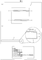
- FIG. 1 is a diagram illustrating a schematic configuration of a light-emitting device according to Embodiment 1.
- FIG. 3 is a diagram showing a light emitting device substrate used in the light emitting device of Embodiment 1.
- FIG. It is a figure for demonstrating the manufacturing process of the board
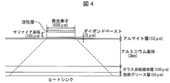
- FIG. 3 is a diagram showing a schematic layer structure of a region where a light emitting element is provided in the light emitting device of the first embodiment.
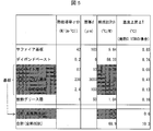
- FIG. 5 is a diagram showing a thermal conductivity ⁇ th, a layer thickness d, a thermal resistance Rth, and a temperature increase ⁇ T corresponding to each layer shown in FIG. 4.
- FIG. 10 It is a figure which shows the schematic layer structure of the area
- FIG. It is a figure which shows the case where the thermal radiation area
- the light-emitting device by arranging a plurality of light emitting elements is a diagram showing a case where considering interference of the radiating region of the light emitting elements adjacent to each other, to adjust the spacing W 0 between the light emitting element 650 .mu.m.
- FIG. 13 is a diagram showing a model structure for obtaining a thermal resistance when the interval W 0 between light emitting elements is adjusted to 650 ⁇ m as shown in FIG.
- the interval (light emitting element closest distance) W 0 between the light emitting elements is changed.
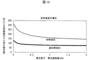
- FIG. 5 is a diagram showing the substrate thermal resistance and the total thermal resistance per light emitting element when the interval W 0 between the light emitting elements is changed when the light emitting device substrate of the present embodiment shown in FIG. 4 is used.
- FIG. 7 is a diagram showing the substrate thermal resistance and the total thermal resistance per light emitting element when the interval W 0 between the light emitting elements is changed when the light emitting device substrate of the comparative example shown in FIG. 6 is used.
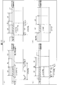
- FIG. 10 is a diagram for explaining a process for manufacturing the light emitting device substrate of the second embodiment.
- 6 is a diagram illustrating a schematic configuration of a light emitting device according to Embodiment 3.
- FIG. It is a figure which shows schematic structure of the illuminating device of Embodiment 3.
- FIG. FIG. 10 is a diagram for describing a manufacturing process of the light-emitting device substrate of Embodiment 4.
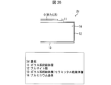
- FIG. 10 is a diagram illustrating a schematic configuration of a light emitting device substrate according to a fifth embodiment.
- FIG. 10 is a diagram showing a schematic configuration of another light emitting device substrate of Embodiment 5.
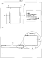
- FIG. 10 is a diagram illustrating a schematic configuration of a light emitting device substrate according to a sixth embodiment.
- FIG. 10 is a diagram showing a schematic configuration of another light emitting device substrate of the sixth embodiment.
- FIG. 5 is a schematic diagram for explaining the reason why the thermal resistance sharply decreases as the thickness of the aluminum substrate increases in the light emitting device of the present embodiment illustrated in FIG. 4.
- FIG. 7 is a schematic diagram for explaining the reason why the value of the thermal resistance is substantially constant even when the thickness of the aluminum base increases in the light emitting device of the comparative example illustrated in FIG. 6.
- Embodiments of the present invention will be described with reference to FIGS. 1 to 29 as follows.
- FIG. 1 shows a schematic configuration of a light-emitting device 1 according to the present embodiment.
- FIG. 1A is a plan view of the light-emitting device 1
- FIG. 1B is a cross-sectional view of the light-emitting device 1.
- the light emitting device 1 is a COB (chip on board) type light emitting device in which a plurality of light emitting elements 7 are mounted on a light emitting device substrate 2.
- COB chip on board
- a light emitting diode (hereinafter referred to as an LED element) is used as the light emitting element 7, but the present invention is not limited to this, and an EL element or the like can also be used.
- a sealing resin peripheral frame 10 surrounding the periphery of the plurality of light emitting elements 7 is provided on the light emitting device substrate 2, and the sealing resin peripheral frame 10 is filled with the sealing resin 9 to form the light emitting elements 7. It is sealed.
- the sealing resin 9 includes a phosphor so that the emitted light from the light emitting element 7 can excite the phosphor to be converted into light having a different wavelength.
- the light emitting device 1 includes the sealing resin 9. The surface emits light on the surface.
- the detailed configuration of the light emitting device substrate 2 will be described later with reference to FIGS. 2 and 3, the detailed configuration of the light emitting device substrate 2 is omitted in FIG. Further, in order to simplify the drawing, the number of the light emitting elements 7 on the light emitting device substrate 2 is greatly omitted. Similarly in the drawings other than FIG. 1, the dimensions are adjusted as appropriate for convenience of description, and therefore, the dimensions may not necessarily indicate the actual number or the actual similarity.
- the input power increases to 10 W, 50 W, 100 W, or 100 W or more, and high-luminance outgoing light can be obtained.
- a medium size LED element of about 650 ⁇ m ⁇ 650 ⁇ m is used as the light emitting element 7, and the light emitting device 1 is realized by integrating the light emitting elements 7 and having a large output of about 100 W. Need to integrate as many as 300 to 400 light emitting elements 7.
- the sealing resin 9 contains a phosphor
- a blue LED element, a purple LED element, an ultraviolet LED element, or the like can be used as the light emitting element 7.
- any one of blue, green, yellow, orange, and red, or a combination of phosphors of any plurality of colors can be used. Thereby, the emitted light of a desired color can be emitted.
- the present invention is not limited to this, and the phosphor is not contained in the sealing resin 9 and the emission wavelength is different.
- the blue, green and red light emitting elements 7 may be arranged on the light emitting device substrate 2, and any two colors of light emitting elements 7 may be arranged on the light emitting device substrate 2. Further, the monochromatic light emitting elements 7 may be arranged on the light emitting device substrate 2.
- a positive electrode connector 3 and a negative electrode connector 4 connected to an external power source are provided on the light emitting device substrate 2, and further, on the light emitting device substrate 2.
- the light-emitting device 1 is a high-luminance type that requires brightness
- a plurality of light-emitting elements 7 are connected in series with wires 8, and a high voltage is supplied from the wires 8 at both ends to emit light.
- the connection method of the light emitting element 7 is not limited to this. (Light Emitting Device Substrate)
- the light emitting device substrate 2 used in the light emitting device 1 will be described with reference to FIG.
- FIG. 2 is a view showing the light emitting device substrate 2
- FIG. 2A is a plan view of the light emitting device substrate 2
- FIG. 2B is a partial enlarged view of a cross section of the light emitting device substrate 2.
- the light emitting device substrate 2 is made of an aluminum substrate 14.
- the aluminum substrate 14 is used.
- the present invention is not limited to this, and any substrate having aluminum as a main component can be used.
- the aluminum substrate 14 having a vertical width of 50 mm, a horizontal width of 50 mm, and a thickness of 3 mm is used.
- the dimensions of the aluminum substrate 14 are not limited to this, and the size of the light-emitting element 7 and the light-emitting element 7 may be appropriately determined in consideration of the degree of integration.
- a base made of aluminum is used as the aluminum base 14, but the base is not limited to this, and the base contains an aluminum component to the extent that anodization of aluminum is possible. That is, an aluminum substrate containing other components to the extent that does not interfere with the anodizing treatment of aluminum can be used.
- a high reflectance coated with the glass-based insulator layer 11 (first insulating layer) and the alumite layer 12 is provided on the surface on one side of the aluminum substrate 14. And a light reflection layer.
- a glass-based insulator layer 13 is provided on at least the other surface of the aluminum substrate 14 (the back surface facing the surface of the aluminum substrate 14 on which the alumite layer 12 is formed). In the present embodiment, the glass-based insulator layer 13 is also provided on the side surface of the aluminum substrate 14.
- the aluminum substrate 14 there is a glass-based insulator layer 11 and a base circuit pattern (not shown in FIG. 2) composed of a conductive layer formed on the glass-based insulator layer 11.
- the negative electrode pattern 6 (or the positive electrode pattern 5) is formed so as to cover the underlying circuit pattern made of the conductive layer.
- the glass-based insulator layer 11 is an insulator layer provided for preventing a short circuit between the aluminum base 14 and the negative electrode pattern 6 (or the positive electrode pattern 5).
- an insulator layer is used in which ceramic particles made of aluminum nitride are covered with glass to lower the thermal resistance. It is not limited to this.
- a ceramic insulator layer may be used instead of the glass-based insulator layer 13.
- ceramic particles may be deposited by spraying ceramic particles onto the aluminum substrate 14 at a high speed.
- a thermal spraying method, an AD method (an aerosol deposition method), and the like can be given as examples of specific manufacturing methods. If the thermal spraying method is used, the substrate temperature during the ceramic layer deposition is about 200 ° C. at the highest, and if the AD method is used, it is about room temperature, which is low in any case. It is possible to easily form a ceramic layer even for such a low melting point metal.
- the glass-based insulator layer 11 is used as the first insulating layer to be formed on one surface of the aluminum base 14, but the present invention is not limited to this.
- the first insulating layer an alumite layer made of an anodized film by alumite treatment (anodization treatment) of the aluminum substrate 14 can also be used.
- the thickness of the alumite layer in this case is not particularly limited as long as it is a thickness necessary for preventing a short circuit between the aluminum base 14 and the negative electrode pattern 6 (or the positive electrode pattern 5).
- FIG. 3 is a view for explaining a manufacturing process of the light emitting device substrate 2 shown in FIG.
- an aluminum substrate 14 having a vertical width of 50 mm and a horizontal width of 50 mm is cut out from an aluminum plate having a thickness of 3 mm, and aluminum nitride is formed on one surface of the aluminum substrate 14 from aluminum nitride.
- a glass-based insulator layer 11 which is an insulator layer in which ceramic particles are covered with glass is provided, and an aluminum substrate 14 and a negative electrode pattern 6 (or positive electrode pattern 5) not shown in FIG. To prevent short circuit.
- a glass system that is an insulating layer in which ceramic particles made of aluminum nitride are covered with vitreous also on the other surface of the aluminum substrate 14 (the back surface facing the surface of the aluminum substrate 14 on which the alumite layer 12 is formed).
- An insulator layer 13 is provided.
- the side surface of the aluminum base 14 is also covered with the glass-based insulator layer 13, but the present invention is not limited to this, and the side surface of the aluminum base 14 is not limited to the glass-based insulator. Instead of covering with the layer 13, it may be covered with the alumite layer 12.
- the exposed portion of aluminum other than the portion covered with the alumite layer 12 in the aluminum base 14 is covered with the glass-based insulator layer 11 and the glass-based insulator layer 13. It becomes.
- the material of the glass-based insulator layer 11 and the material of the glass-based insulator layer 13 are the same, but are not limited thereto, and the material of the glass-based insulator layer 11 is not limited to this.
- the glass insulator layer 13 may be made of different materials.
- the film thickness of the glass-based insulator layer 11 is not particularly limited as long as it is a thickness necessary for preventing a short circuit between the aluminum base 14 and the negative electrode pattern 6 (or the positive electrode pattern 5), but is approximately 50 ⁇ m or more. It is desirable.
- the film thickness of the glass-based insulator layer 13 is preferably about 50 ⁇ m to 150 ⁇ m in consideration of the withstand voltage and heat dissipation of the light emitting device substrate 2.
- the film thickness of the glass insulator layer 13 is preferably about 50 ⁇ m to 150 ⁇ m in consideration of the withstand voltage and heat dissipation of the light emitting device substrate 2.
- the glass-based insulator layer 11 and the glass-based insulator layer 13 illustrated in FIG. 3A are formed on the aluminum base 14. After applying the raw material, it can be formed by firing.
- a ceramic paint containing ceramic particles made of high-temperature fired aluminum nitride and a glass raw material is applied to the aluminum substrate 14 or After printing, glass is synthesized from a glass raw material by a sol-gel method to form a glass-based insulator layer 11 and a glass-based insulator layer 13 which are insulator layers in which ceramic particles made of aluminum nitride are covered with glass. .
- the glass insulator layer 11 and the glass insulator layer 13 are formed by using a method of synthesizing glass from a glass raw material by a sol-gel method, whereby a heat treatment at a relatively low temperature of 250 ° C. to 500 ° C. is performed.
- the glass-based insulator layer 11 and the glass-based insulator layer 13 made of a ceramic layer using a glass-based binder can also be formed by the process.
- the temperature at which a ceramic raw material made of aluminum nitride is fired is usually a high temperature of 1200 ° C. to 1400 ° C.
- the high temperature fired ceramic is made into particles and then contained in a normal glass-based binder.
- ordinary glass-based binders go through a high-temperature molten state, and therefore the firing temperature needs to be heat-treated at a fairly high temperature of about 900 ° C.
- the melting point of aluminum of the aluminum substrate 14 used in the present embodiment is about 660 ° C., the aluminum substrate 14 cannot withstand such a high temperature process.
- a method of directly synthesizing glass without using a high-temperature molten state by a sol-gel method from a glass raw material is used, and by using such a method,
- the glass-based insulator layer 11 and the glass-based insulator layer 13 made of a ceramic layer using a glass-based binder are also formed by a heat treatment process at 250 ° C. to 500 ° C., which is a process temperature lower than the melting point of aluminum of about 660 ° C. be able to.
- aluminum can be used as the base material of the light emitting device substrate 2 by using a method of synthesizing glass from a glass raw material by a sol-gel method.
- particles made of aluminum nitride are mixed as ceramics.
- the present invention is not limited to this.
- particles composed of at least one of aluminum nitride, alumina, zirconia, and titanium oxide may be mixed.
- silica (SiO 2 ) particles may be mixed with a glass binder to form a glass insulator layer.
- ceramic particles may be further mixed.
- the glass-based insulator layer raw material uses a sol-like glass raw material as a ceramic binder, and the glass component that appears after gelation by drying is further baked to produce a ceramic. Since it has heat resistance and withstand voltage resistance similarly to the above, it is preferably used as an insulating material for a light emitting device substrate. In particular, when the input power of the light emitting device is 10 W to 100 W or more, the light emitting device substrate also becomes high temperature due to the heat generated by the light emitting element. Therefore, a stable substance such as glass is used as the insulating material of the light emitting device substrate. It is preferable to use it. Again, silica (SiO 2 ) particles, which are glass components, may be added to a glass-based binder that is a raw material for sol-like glass.
- the ceramic does not hinder the dielectric strength of the glass material but lowers the thermal resistance.
- the presence or absence of light absorption of the ceramics to be mixed is not particularly specified.
- black particles such as silicon carbide (SiC) and silicon nitride (Si 3 N 4 ) may be used.
- the ceramic is not limited to a metal oxide, and may be a more general inorganic solid other than a metal oxide such as aluminum nitride, silicon carbide, or silicon nitride. As long as it is a stable inorganic solid material that lowers the thermal resistance, it does not impede the insulation withstand voltage.
- such a glass-based insulator layer may be a single vitreous film formed without mixing ceramic particles.
- glassy silica (SiO 2 ) particles may be further contained in the glassy film.
- glass binder in glass-based insulator layer Glass binder
- a glass binder (glassy) in a glass-based insulator layer provided on the light emitting device substrate of the present embodiment that is, a glass binder (glassy) formed by a sol-gel method will be described.
- a pre-stage substance that forms a glassy material such as organic polysiloxane is used as a raw material in a sol state, and a chemical reaction is advanced at a temperature of 250 ° C. to 400 ° C. (500 ° C.) without passing through a molten state.
- the glass-based insulator layer can be formed by directly converting to glass.
- the raw material in the sol state is dried at a relatively low temperature, the polycondensation is repeated, and a three-dimensional structure network is formed and converted into a gel state and vitrified.
- a three-dimensional structure network is formed and converted into a gel state and vitrified.
- it is porous and weak as a film. Therefore, for example, high-temperature heat treatment (firing) at 400 ° C. to 500 ° C. is performed. By this firing, pores in the gel disappear, and a dense glass-based insulator layer can be formed.
- a metal alkoxide such as tetraethoxysilane (Si (OCH 2 CH 3 ) 4
- sol-like substances obtained by decomposition and condensation polymerization.
- organic polysiloxane and its condensate may be sufficient, for example.
- the glass-based insulator including a sintered body obtained by coating or printing a sol-like substance mixed with ceramic particles on a substrate and then gradually drying and sintering at about 250 ° C. to 400 ° C. (500 ° C.). A layer can be obtained.
- the sol-like substance may have an alkoxyl group represented by an ethoxy group, a methoxy group or the like.
- the condensation reaction proceeds appropriately by using an acid catalyst and the temperature is further raised, and a network having a three-dimensional structure is formed and gelled. Furthermore, by baking the gelled material, the pores remaining in the gel disappear and a dense and stable glass-based insulator layer is obtained.
- a metal oxide or metal hydroxide is mixed appropriately to soften the glass. Or the melting point may be lowered.
- the method of mixing oxides is a method widely used in general glass manufacturing other than the sol-gel method, and the metal oxide to be added is boron oxide, which is also used in borosilicate glass. Typical examples include sodium oxide and aluminum oxide. Further, a hydroxide containing boron, sodium, aluminum, or the like may be added.
- silica (SiO 2 ) particles that are already stable as glassy material are added to the sol-like substance (sol-like binder) and fired. May be.
- the raw material already contains glass, but since normal silica particles are stable, stable silica particles (glassy) may not be enveloped by newly formed glass.
- stable silica particles (glassy) may not be enveloped by newly formed glass. Therefore, it is judged that it is difficult to form a new chemical bond between the stable silica particles (glassy) and the newly formed glassy material. Therefore, when stable silica particles (glassy) are added, the silica particles are considered to be particles whose periphery is hardened with a glass binder, like ceramic particles.
- the glass binder can be formed using a normal method other than the sol-gel method.
- the raw materials used in such a normal method are different from the raw materials used in the sol-gel method described above, and glass particles are already mixed as raw materials at the time of printing on the substrate.
- the glass particles in the raw material are remelted by firing and then cured to obtain a dense and smooth glass-based insulator layer on the substrate.
- a glass binder glassy
- particles of a low-melting glass in a particulate form obtained by pulverizing a low-melting glass prepared in a molten state or by vapor phase growth are used as an organic binder, an organic solvent Etc. to prepare a paste.
- the prepared paste is printed on a substrate and fired at a high temperature of around 800 ° C. Then, the resin and the organic solvent used for the organic binder disappear due to evaporation and combustion, and only the glass particles are remelted and then cured on the substrate to obtain a dense and smooth glass-based insulator layer.
- the vitreous material that has been taken in and remelted by the glass-based insulator layer serves as a binder for these particles.
- a ceramic paint containing ceramic particles and a glass raw material is used as a raw material for the glass-based insulator layer 11 and the glass-based insulator layer 13, but in such a case, a glass-based insulating material is used.
- the weight percentage of the ceramic particles in the body layer is preferably 50% -90% when the glass-based insulator layer is completed. The reason will be described below.
- ceramics have higher thermal conductivity than glass, so when using ceramics as a glassy sealed glass-based insulator layer, trying to increase the thermal conductivity of the insulator layer This is because it is necessary to suppress the amount of glass binder (glassy) as much as possible and increase the amount of ceramic.
- Ceramics having high thermal conductivity is aluminum nitride particles used in the present embodiment.
- the aluminum nitride particles occupy 50% or more by weight of the glass-based insulator layer formed by sealing the aluminum nitride particles with a glass binder (glassy)
- the effect of increasing the thermal conductivity is noticeable. Initially, the thermal conductivity monotonously increases until it exceeds 90% by weight in the finally obtained glass-based insulator layer.
- the weight percentage of the ceramic particles in the glass-based insulator layer is desirably 50% -90%.
- Whether it should be used as a glass-based insulator layer by using glass alone without mixing ceramics or as a glass-based insulator layer mixed with ceramics depends on the specific conditions under which the substrate is used. It only has to be decided.
- the glass-based insulator layer may be formed by mixing glass particles such as silica particles in a glass binder. Since silica particles themselves are stable glassy, mixing silica particles contributes to the formation of a glass-based insulator layer having stable characteristics.
- the exposed aluminum portion other than the portion covered with the glass-based insulator layer 11 and the glass-based insulator layer 13 is an alumite layer 12. Covered.
- the light reflecting layer made of the aluminum substrate 14 coated with the alumite layer 12 can prevent corrosion due to oxidation of the aluminum substrate 14, and thus can maintain a high light reflectance over a long period of time.
- an alumite layer 12 made of an anodized film by anodizing (anodizing treatment) of the aluminum substrate 14 is formed as shown in FIG. Can be formed.
- the alumite layer 12 thus formed is very hard and excellent in durability.
- the alumite layer 12 is formed to have a film thickness of 5 ⁇ m to 10 ⁇ m, and is relatively thin with a thickness of about 30 ⁇ m even when it is thick.
- the thermal conductivity of alumite is approximately 67 W / (m ⁇ K), which is only about 1/3 compared to the thermal conductivity of aluminum 236 W / (m ⁇ K), but the thermal conductivity of glass ( Compared to about 1 W / (m ⁇ K)) and the thermal conductivity of silicone resin (0.15 to 0.30 W / (m ⁇ K)), the conductivity is relatively high.
- a sealing process is performed after the anodizing process, that is, after the formation of the anodized layer 12 in order to close the porous holes generated in the anodized layer 12 that is an anodized film.
- the sealing process is performed after the anodizing treatment, the anodized layer 12 which is an aluminum anodized film is stabilized, and the durability, corrosion resistance and erosion resistance of the aluminum substrate 14 are further improved.
- the light reflecting layer composed of the aluminum substrate 14 covered with the alumite layer 12 can maintain a high light reflectance over a long period of time.
- the sealing treatment may be performed according to a normal method in this field, and a typical method is sealing treatment in boiling water. That is, after forming the anodized film, the alumite layer 12 is sufficiently washed with water and kept in pure water for about 30 minutes. This method has a high work efficiency because a large number of substrates can be processed at one time.
- This sealing treatment may be performed if necessary according to the film formation state of the alumite layer 12 and is not necessarily performed.
- the alumite layer 12 by anodic oxidation after the formation of the glass-based insulator layer 11 and the glass-based insulator layer 13 as in the present embodiment.
- the glass-based insulator layer 11 and the glass-based insulator layer 13 after applying or printing a ceramic paint containing ceramic particles and glass raw material fired at a high temperature on the aluminum substrate 14.
- the glass-based insulator layer 11 and the glass-based insulator layer 13 are formed by synthesizing glass from a glass raw material by a sol-gel method.
- the firing temperature at this time is lower than the melting point of aluminum of about 660 ° C., and 250 ° C. ⁇ 500 ° C.
- the anodized layer 12 made of an anodized film is heated to this temperature and baked, the anodized layer 12 is cracked, and a plating solution is used in the plating process in the step of forming an electrode pattern as a subsequent step. Therefore, not only the function of protecting the aluminum substrate 14 is remarkably deteriorated, but also the function as a protective film for preventing oxidation, corrosion and erosion is similarly lowered. Furthermore, the function as an electrical insulating layer is also reduced.
- the glass-based insulator layer 11 and the glass-based insulator layer 13 are It serves as a mask at the time of anodizing treatment, and the aluminum base 14 is not covered with the glass-based insulator layer 11 and the glass-based insulator layer 13, but only the exposed portion is covered with the alumite layer 12. Become.
- the aluminum base 14 is immersed in a chemical solution and energized to form the anodized layer 12. Therefore, the aluminum exposed surface of the aluminum base 14 is entirely covered with anodized. . For this reason, when the glass-based insulator layer 11 and the glass-based insulator layer 13 are formed after the formation of the alumite layer 12, in order to avoid the above-described peeling problem, a part of the aluminum base 14 is formed. Anodizing is performed to form the alumite layer 12 only on a part of the aluminum substrate 14 or anodizing is performed on the entire aluminum substrate 14 to form the alumite layer 12 on the entire aluminum substrate 14. There is no choice but to remove the alumite layer 12 in the region where the glass insulator layer 11 and the glass insulator layer 13 are to be formed.
- the formation of the anodized layer 12 by the anodizing treatment should be performed after the formation of the glass-based insulator layer 11 and the glass-based insulator layer 13. Is preferred.
- the glass-based insulator layer 11 and the glass-based insulator layer 13 are formed at the same time, but the present invention is not limited to this, and the glass-based insulator layer 11 and the glass-based insulating layer are not limited thereto.
- the body layer 13 may be formed separately, or may be performed by a convenient formation procedure of the manufacturing apparatus. (Polishing process before anodizing to increase the brightness of the light reflecting surface)
- a step of polishing the surface of the aluminum base 14 is performed before the anodizing treatment.
- the surface of the aluminum substrate 14 is polished by a buffing method, a chemical polishing method, an electrolytic polishing method or the like and then anodized, a high-brightness reflecting surface with high light reflectance can be obtained.
- polishing is performed by electrolytic polishing as final polishing.
- polishing may be performed by a chemical polishing method.
- the light incident on the light reflecting surface of the aluminum substrate 14 covered with the anodized layer 12 is reflected or scattered by the anodized aluminum film (anodized layer 12) or transmitted through the anodized layer.
- Light transmitted through the alumite layer and reaching the aluminum substrate is reflected or scattered by the upper surface of the aluminum substrate.
- the unevenness of the surface of the aluminum substrate 14 can be eliminated before the anodizing treatment, and the surface finish after the anodizing treatment can be cleaned. That is, when the anodizing treatment is performed after the aluminum substrate is polished, the smoothness of the upper surface of the aluminum substrate is also improved, so that scattering can be suppressed, so that a highly reflective substrate can be realized. Further, when the anodization is performed after polishing the aluminum substrate, the smoothness of the anodized film formed on the upper surface of the aluminum substrate with improved smoothness is also improved. And a highly reflective substrate can be realized.
- the buffing method and the electropolishing method are used in combination.
- the polishing step includes the buffing method, the chemical polishing method, and the electropolishing method. It can be performed using at least one of them.
- the polishing step is performed before the anodizing treatment, but the polishing step may be performed before the glass-based insulator layer 11 is formed.
- the aluminum base 14 is provided with a light reflecting surface having a high light reflectivity protected by the alumite layer 12, and the aluminum base 14 includes the glass-based insulator layer 11 and glass.
- the light emitting device substrate 2 that is covered with the system insulator layer 13 and has high light reflectivity, high heat radiation heat resistance, and high withstand voltage can be realized.
- FIG.3 (c) and FIG.3 (d) the manufacturing procedure of the positive electrode pattern 5 and the negative electrode pattern 6 is demonstrated.
- a glass-based insulator layer is formed on one surface of the aluminum base 14 for the purpose of preventing a short circuit between the aluminum base 14 and the positive electrode pattern 5 or the negative electrode pattern 6. 11 is formed.
- the glass-based insulator layer 11 is used for the purpose, the present invention is not limited to this, and depending on the purpose and application of the light-emitting device substrate 2, an insulator layer can be used instead of the glass-based insulator layer 11.
- An alumite layer 12 can also be used.
- the insulator layer can be formed as a series with the alumite layer 12.
- a metal paste made of resin containing metal particles is used as a base for the electrode pattern on the glass-based insulator layer 11. Then, a circuit pattern was drawn by printing or the like and dried to form an underlying circuit pattern 15.
- the surface of the underlying circuit pattern 15 is thinly covered with resin (coating resin layer), plating does not deposit on the surface of the underlying circuit pattern 15 in this state. Therefore, the resin on the surface of the underlying circuit pattern 15 was removed by etching (removal of the coating resin layer) to expose the conductive layer of the underlying circuit pattern 15.
- the aluminum base 14 Since the entire aluminum base 14 is already covered with the alumite layer 12, the glass-based insulator layer 11, and the glass-based insulator layer 13, the aluminum base 14 is eroded by the plating solution used in the plating process. It will never be done. Furthermore, since the aluminum substrate 14 is covered with the anodized layer 12, the glass-based insulator layer 11, and the glass-based insulator layer 13, which are electrically insulating materials, only the base circuit pattern 15 is made from the plating solution. It becomes possible to deposit the metal for electrode formation efficiently. (Thermal analysis results of light emitting device and light emitting device substrate) In the following, based on FIGS.
- one surface of the aluminum base has a function as a light reflecting surface, and high heat dissipation is achieved by the other surface facing the one surface of the aluminum base.
- a substrate for a light-emitting device according to the present embodiment which is designed to ensure withstand voltage resistance, and a ceramic paint containing a high-temperature fired ceramic and a glass raw material that bears the light reflection function and the withstand voltage function in the same layer. The result of thermal analysis of the substrate for a light emitting device of the comparative example applied on one surface of the aluminum substrate is compared.
- a glass-based insulator layer formed of a ceramic paint containing high-temperature fired ceramics and glass raw materials can provide high reflectivity and high dielectric strength, but the thermal resistance of the vitreous material used as the binder Therefore, the thermal conductivity of the glass-based insulator layer thus obtained is approximately 1 to 3 W / (m ⁇ ° C.), which is 1 digit lower than that of ordinary ceramics and 2 digits lower than that of metal. End up.
- a film thickness of about 100 ⁇ m is required.
- the thermal resistance is high (the heat dissipation is poor), There was a problem that the temperature rise was likely to increase.
- FIG. 4 is a diagram showing a schematic layer structure of a region where a light emitting element is provided in the light emitting device of this embodiment
- FIG. 5 shows thermal conductivity ⁇ th corresponding to each layer shown in FIG. , Layer thickness d, thermal resistance Rth, and temperature rise ⁇ T.
- a light emitting element is disposed on a light emitting device substrate, and the light emitting device substrate has a three-layer structure (an alumite layer, an aluminum substrate, and a glass-based insulator layer).
- the middle layer of the light emitting device substrate is made of an aluminum substrate having a thickness of 3 mm, and the upper surface of the aluminum substrate is coated with an alumite layer having a thickness of 10 ⁇ m so that the upper surface of the aluminum substrate is a reflective surface.
- the lower surface of is covered with a glass-based insulator layer having a thickness of 100 ⁇ m formed of a ceramic paint containing high-temperature fired ceramics and a glass raw material.
- the light emitting element is arrange
- the planar size of the light emitting element is 650 ⁇ m in length and 650 ⁇ m in width, the thickness from the die bond paste layer to the active layer of the light emitting element is 100 ⁇ m, and the light emitting element substrate is made of sapphire. An element substrate was used.
- the value of the thermal resistance of the light emitting device depends on the position and dimensions of the heat source, in the result of the thermal resistance Rth shown in FIG. 5, it is assumed that the active layer of the light emitting element is the only heat source. Rth is calculated. Further, in FIG. 5, not only the thermal resistance Rth of each layer but also the temperature rise ⁇ T of each layer is obtained. This temperature rise ⁇ T is a value when the heat generation amount of the heat source is assumed to be 0.15 W.
- the spread of heat in the lateral direction was taken into consideration. Specifically, as shown by a broken line in FIG. 4, it was obtained on the assumption that heat is uniformly diffused so as to spread in the 45 ° direction to the left and right with respect to the vertical direction of the substrate.
- thermal resistance Rth and the temperature rise ⁇ T are obtained.
- a substrate having a thermal conductivity ⁇ th (W / (m ⁇ ° C.)) and a layer thickness d (m) has a side size a (m).
- Rth (° C./W) d/( ⁇ th ⁇ a ⁇ (a+2d))
- Q (W) is a calorific value at the heat source.
- the thermal resistance Rth and temperature increase ⁇ T of each layer shown in FIG. 5 are obtained by calculation in this way.
- FIG. 6 shows a ceramic coating containing a high-temperature fired ceramic and a glass raw material, which has a light reflection function and a dielectric strength function in the same layer, for comparison with the light emitting device of the present embodiment shown in FIG.
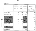
- FIG. 7 is a diagram showing a schematic layer structure of a region where a light emitting element is provided in a light emitting device of a comparative example applied on one surface of an aluminum substrate, and FIG. 7 shows heat corresponding to each layer shown in FIG.
- the conductivity ⁇ th, the layer thickness d, the thermal resistance Rth, and the temperature rise ⁇ T are shown.
- the middle layer of the light emitting device substrate of the comparative example is made of a 3 mm-thick aluminum base, and the upper surface of the aluminum base has a thickness of 100 ⁇ m having a light reflection function and a withstand voltage function.
- a glass-based insulator layer is formed, and an alumite layer having a thickness of 10 ⁇ m is formed as a protective film on the lower surface of the aluminum base. Therefore, the substrate for a light emitting device of the comparative example has a three-layer structure (a glass-based insulator layer, an aluminum substrate, and an alumite layer).
- the required material, the required film thickness, and the thermal conductivity are different from each other.
- the thermal conductivity is 2.4 W / (m ⁇ ° C.)
- the film thickness is 100 ⁇ m
- the layers are made of the same material.
- the total thermal resistance obtained between the sapphire substrate immediately below the active layer of the light emitting element and the heat dissipating grease layer directly above the heat sink for heat dissipation. Is 68.9 ° C./W.
- the thermal resistance of the light emitting device substrate having a three-layer structure is 3.9 ° C./W, and the contribution ratio is only 6% with respect to the total thermal resistance. Only.
- the thermal resistance of the conventional light emitting device substrate having a three-layer structure is 75.6 ° C./W, and the light emitting device substrate of the comparative example with respect to the total thermal resistance.
- the contribution ratio of thermal resistance is 54%.
- the total thermal resistance of the light emitting device of this embodiment illustrated in FIG. 4 is 68.9 ° C./W, and the total thermal resistance of the light emitting device of the comparative example illustrated in FIG. 6 is 140.5 ° C./W.
- the total thermal resistance of the light emitting device of this embodiment is only 49% of the total thermal resistance of the conventional light emitting device.
- the thermal resistance of the light emitting device substrate of the light emitting device of the present embodiment shown in FIG. 4 is 3.9 ° C./W, and the thermal resistance of the light emitting device substrate of the comparative light emitting device shown in FIG. Is 75.6 ° C./W, the thermal resistance of the light emitting device substrate of the light emitting device of this embodiment is only 5% of the thermal resistance of the light emitting device substrate of the comparative light emitting device.
- the thermal resistance of the light-emitting device substrate of the light-emitting device of this embodiment is remarkably improved as far as the light-emitting device substrate is concerned.
- the layer having the highest effect of improving the thermal resistance is a glass-based insulator layer.
- a glass-based insulator layer having a low thermal conductivity of 2.4 W / (m ⁇ ° C.) and a thickness of 100 ⁇ m laid directly under the light emitting element is formed as shown in FIG.
- the thermal resistance of this layer can be drastically reduced from 73.41 ° C./W to only 0.89 ° C./W, that is, about 1/80, by simply pulling it away from the aluminum substrate and transferring it to the lower surface of the aluminum substrate.
- the thermal resistance of each layer completely changes depending on where the layer is disposed on the light emitting device substrate and whether the layer is near or far from the heat source. It is. This can be explained by the size of the cross-sectional area of the cross section of the passage when heat crosses each layer.
- the horizontal heat diffusion region of the light emitting device substrate is schematically shown by broken lines in FIGS. Show.
- the area surrounded by the broken line corresponds to a heat path, and the more the broken line goes to the lower layer, the more the heat spreads in the vertical direction of the light-emitting device substrate and gradually diffuses in the horizontal direction.
- the cross-sectional area of the passage of heat across the glass-based insulator layer having a low thermal conductivity of 2.4 W / (m ⁇ ° C.) is wide in FIG. 4 and narrow in FIG. For this reason, the thermal resistance of the glass-based insulator layer shown in FIG.
- the glass-based insulator layer illustrated in FIG. 4 is farther from the heat source by 3.0 mm than the glass-based insulator layer illustrated in FIG. Comparing the cross-sectional areas of the heat paths in the layers with average values in the layers, the glass-based insulator layer shown in FIG. As a result, the thermal resistance was reduced to about 1/80.
- the cross-sectional area of the heat path in this layer is It is almost the same as the light emitting element size.
- the aluminum base is horizontal before passing through the aluminum base. Since the heat is sufficiently diffused in the direction, the cross-sectional area of the heat passage is very large in the glass-based insulator layer, and the thermal resistance can be lowered.
- the thermal conductivity of the glass-based insulator layer is 2.4 W / (m ⁇ ° C.), whereas the thermal conductivity of the aluminum substrate is 236 W / (m ⁇ ° C.), which is 100 times higher. The effect on total thermal resistance is negligible.
- the thermal resistance is remarkably lowered only by transferring the glass-based insulator layer on the upper surface of the aluminum substrate to the lower surface of the aluminum substrate as shown in FIG. Became clear.
- the glass-based insulator layer in FIG. 6 functions as a light reflecting layer as well as an insulating layer, an alternative structure that bears the light reflecting function is required when this layer is moved. .
- the characteristics required for this alternative structure are high light reflectance, low thermal resistance, and stability. That is.
- the light reflecting surface obtained by coating the above-described aluminum substrate with an alumite layer is optimal.
- the thickness of the aluminum substrate is fixed to 3 mm, and the thermal resistance and temperature rise are compared with the configuration of the comparative example.
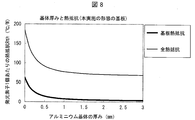
- FIG. 8 is a diagram showing the dependence of the thermal resistance on the thickness of the aluminum substrate in the light emitting device of the present embodiment shown in FIG. 4, and FIG. 9 is a comparative light emitting device shown in FIG. It is a figure which shows the thickness dependence of the aluminum base
- the vertical axis shows the aluminum substrate thickness (mm) shown on the horizontal axis in the light emitting device of this embodiment and the comparative example. It shows how the thermal resistance (° C./W) changes.
- the calculation conditions used here are the same as those used when calculating the thermal resistance with the above-mentioned aluminum substrate thickness fixed at 3 mm.
- required here is a value per light emitting element, and calculated
- the total thermal resistance here refers to the thermal resistance from the active layer of the light emitting element to the heat sink, and the thermal resistance caused by the light emitting device substrate is called the substrate thermal resistance.
- the total thermal resistance of the light emitting device of the present embodiment is more drastically reduced as the thickness of the aluminum substrate is increased than the light emitting device of the comparative example.
- the substrate thermal resistance when the thickness of the aluminum substrate increases, the value of the thermal resistance sharply decreases in the light emitting device of the present embodiment, whereas in the light emitting device of the comparative example, the thermal resistance of The value is almost constant, and in detail, gradually increases from 74 ° C./W to 76 ° C./W.
- FIG. 28 is a schematic diagram for explaining the reason why the thermal resistance rapidly decreases as the thickness of the aluminum substrate increases in the light emitting device of the present embodiment shown in FIG.
- FIG. 28 (a) is a diagram showing a case where the aluminum substrate is thin
- FIG. 28 (b) is a diagram showing a case where the aluminum substrate is thick.
- FIG. 29 is a schematic diagram for explaining the reason why the value of the thermal resistance is substantially constant even if the thickness of the aluminum substrate is increased in the light emitting device of the comparative example shown in FIG.
- FIG. 29 (a) is a diagram showing a case where the thickness of the aluminum substrate is thin
- FIG. 29 (b) is a diagram showing a case where the thickness of the aluminum substrate is thick. This will be described below by comparing FIG. 28 and FIG.
- the active layer, the sapphire substrate, the die bond paste, and the alumite layer are not shown.
- the glass-based insulator layer having a low thermal conductivity is disposed on the lower surface of the aluminum substrate, and compared to the schematic diagram of FIG. In a remote location. Therefore, as shown in FIG. 28, the thickness tsub (a) of the aluminum substrate in FIG. 28 (a) is increased to the thickness tsub (b) of the aluminum substrate in FIG. 28 (b). As a result, both the glass-based insulator layer and the heat dissipating grease layer can be moved away from the light emitting element, and as a result, both the substrate thermal resistance and the total thermal resistance can be reduced.
- the thermal conductivity of the aluminum substrate is sufficiently high compared to the glass-based insulator layer and the heat dissipating grease layer, which are layers having low thermal conductivity, the contribution to the thermal resistance is small. Therefore, when the thickness of the aluminum substrate having high thermal conductivity is increased (from the aluminum substrate thickness tsub (a) in FIG. 28 (a) to the aluminum substrate thickness tsub (b) in FIG. 28 (b)), FIG. 28 (b), the width of the heat passage is widened by the glass-based insulator layer and the heat dissipating grease layer, which are layers having low thermal conductivity (from L3 (a) in FIG. 28 (a)). (L3 (b) in FIG. 28B). Accordingly, the cross-sectional area of the path through which heat passes increases, and the thermal resistance is inversely proportional to the cross-sectional area of the thermal path, so the thermal resistance decreases.
- the glass-based insulator layer is disposed on the upper surface of the aluminum base and emits light as a heat source. It will be located in the vicinity of the element (heating element). And it is a thermal radiation grease layer arrange
- the thermal conductivity of the aluminum substrate is sufficiently high compared to the glass-based insulator layer and the heat dissipating grease layer, which are layers having low thermal conductivity, the contribution to the thermal resistance is small. Accordingly, the thickness of the aluminum substrate having high thermal conductivity is increased (from the aluminum substrate thickness tsub (a) in FIG. 29A to the aluminum substrate thickness tsub (b) in FIG. 29B).
- the glass-based insulator layer has a constant heat passage width (FIGS. 29A and 29 (A) and 29 (B). L1) in b).
- the thermal resistance is inversely proportional to the cross-sectional area of the thermal path. Therefore, the thermal resistance is constant even when the thickness of the aluminum substrate is increased. It becomes.
- the thickness of the aluminum substrate is increased (from the thickness tsub (a) of the aluminum substrate in FIG. 29A to the thickness tsub (b) of the aluminum substrate in FIG. 29B), the aluminum substrate is disposed on the lower surface of the aluminum substrate.
- the width of the heat passage is widened (from L3 (a) in FIG. 29 (a) to L3 (b) in FIG. 29 (b)). Therefore, the thermal resistance decreases in the heat dissipating grease layer.
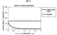
- FIG. 10 is a diagram collectively showing only the substrate thermal resistance, which is the thermal resistance caused by the light emitting device substrate in FIGS. 8 and 9.
- the substrate thermal resistance in the light emitting device of the present embodiment is indicated by a solid line, and the substrate thermal resistance in the comparative light emitting device is indicated by a broken line.
- the substrate thermal resistance when the thickness of the aluminum substrate is 0.1 mm is 41 ° C./W (configuration of the present embodiment) and 74 ° C./W, respectively.
- the substrate thermal resistance when the thickness of the aluminum substrate is 0.5 mm is 15 ° C./W (configuration of the present embodiment) and 75 ° C./W (configuration of the comparative example).
- the substrate thermal resistance when the thickness of the aluminum substrate is 1 mm is 8 ° C./W (configuration of the present embodiment) and 75 ° C./W (configuration of the comparative example), respectively.
- the substrate thermal resistance when 3 mm is 3 mm is 4 ° C./W (configuration of the present embodiment) and 76 ° C./W (configuration of the comparative example), respectively.
- the aluminum base has a thickness of 55% when the thickness is 0.1 mm.
- the thickness of the substrate becomes 0.5 mm, it cuts 19% and 20%, and when the thickness of the aluminum substrate is 1 mm, it becomes 10%, and when the thickness of the aluminum substrate is 3 mm, it becomes only 5%.
- the thickness of the aluminum substrate is fixed at 3 mm and the thermal resistance is obtained, it is effective to reduce the thermal resistance by separating the glass-based insulator layer having a low thermal conductivity from the heat source already described.
- the consideration has become clearer from the relationship between the thermal resistance and the thickness of the aluminum substrate shown in FIG. 10 and the schematic diagrams shown in FIGS. (Light-emitting device with a plurality of light-emitting elements arranged)
- thermal resistance in a light emitting device in which a plurality of light emitting elements are arranged will be examined.
- the heat resistance can be obtained for the heat radiation area indicated by the broken line without considering the heat radiation of the adjacent light emitting elements.
- the light emitting elements are arranged adjacent to each other on the light emitting device substrate, the light emitting elements may overlap with each other and may interfere with each other.
- FIG. 11 is a diagram illustrating a case where a heat dissipation area overlaps between adjacent light emitting elements in a light emitting device in which a plurality of light emitting elements are arranged.
- the heat radiation regions of adjacent light emitting elements indicated by broken lines overlap and interfere with each other. In consideration of such interference, it is necessary to correct the heat flow from the individual light emitting elements.
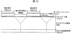
- FIG. 12 is a diagram illustrating a case where the interval W 0 between the light emitting elements is adjusted to 650 ⁇ m in consideration of the interference of the heat radiation area between adjacent light emitting elements.
- the heat flowing region is corrected so that the heat radiation region between adjacent light emitting devices indicated by a broken line does not overlap.
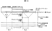
- FIG. 13 is a diagram showing a model structure for obtaining the thermal resistance when the interval W 0 between the light emitting elements is adjusted to 650 ⁇ m as shown in FIG.
- the thermal resistance Rth of the light emitting device substrate per light emitting element was obtained from the configuration of the light emitting device of the present embodiment shown in FIG.
- the thermal resistance Rth of the light-emitting device substrate per light-emitting element in the light-emitting device in which the plurality of light-emitting elements of this embodiment are arranged with the interval W 0 being 650 ⁇ m is obtained from the model structure shown in FIG.
- the interval W 0 between the light emitting elements is set to 650 ⁇ m
- modeling is performed so that interference does not occur in the heat radiation area between adjacent light emitting elements.
- the correction also holds with respect to the spacing W 0 of any of the light emitting element, the interval W 0 between the light emitting element is not limited to 650 .mu.m.
- FIG. 14 shows the thermal resistance Rth and the temperature rise ⁇ T obtained from the thermal conductivity ⁇ th and the layer thickness d corresponding to each layer based on the model structure shown in FIG.
- the configuration of the light emitting device of the comparative example illustrated in FIG. 6 is similarly based on the model structure in which the interval W 0 between the light emitting elements is adjusted, and the thermal conductivity ⁇ th and the layer thickness d corresponding to each layer. From these, the thermal resistance Rth and the temperature rise ⁇ T can be obtained.
- FIG. 15 shows the distance between the light emitting elements (light emitting element closest distance) W 0 when the light emitting device substrate of the present embodiment shown in FIG. 4 and the light emitting device substrate of the comparative example shown in FIG. 6 are used. It is a figure which shows the board
- the heating elements when the heating elements are arranged on the substrate, the relationship between the thermal resistance Rth per light emitting element and the interval W 0 between the light emitting elements is shown in the substrate of the light emitting device of this embodiment and the comparative example. In comparison with the substrate for the light emitting device, it is indicated by a solid line and a broken line.
- the planar dimension of one heating element was 650 ⁇ m ⁇ 650 ⁇ m
- the thickness tg of the glass-based insulator layer was 100 ⁇ m. 15 shows only the substrate thermal resistance, the total thermal resistance will be described later with reference to FIG.
- the thermal resistance Rth of the substrate for the light emitting device of the present embodiment is compared in the region where the interval between the light emitting elements (light emitting element closest distance) W 0 is W 0 ⁇ 2 ⁇ tg.
- the thermal resistance Rth of the substrate for the light emitting device of the example is greatly improved.
- the thermal resistance decreases in the range of W 0 ⁇ 2 ⁇ ds with respect to the thickness ds of the aluminum base in the light emitting device substrate of the present embodiment.
- the thermal resistance becomes constant when W 0 ⁇ 2 ⁇ ds.
- the thickness ds of the aluminum base is determined, if the relationship of W 0 ⁇ 2 ⁇ ds is established with respect to the interval W 0 between the light emitting elements, the influence of heat dissipation between the adjacent light emitting elements is established. Will disappear. Specifically, for example, when the thickness of the aluminum substrate is 3 mm, the interval between the light emitting elements corresponds to 6 mm or more, and at this time, ideal heat dissipation can be realized.
- the light-emitting device substrate of the present embodiment heat The resistance can be lowest. Specifically, when the interval W 0 between the light emitting elements is fixed at 1 mm, it can be said that the thermal resistance is substantially constant if the thickness of the aluminum substrate is 0.5 mm or more. Since the aluminum substrate has a high thermal conductivity, even if the thickness of the aluminum substrate is increased, the influence on the thermal resistance is negligible at a common sense thickness, for example, within 10 mm or within 5 mm.
- the thermal resistance Rth of the light emitting device substrate of the present embodiment is greatly improved over the thermal resistance Rth of the light emitting device substrate of the comparative example in a region where W 0 ⁇ 2 ⁇ tg will be described.
- FIG. 16 is a schematic diagram when light emitting elements are arranged on the light emitting device substrate of the present embodiment in which a glass-based insulator layer having a low thermal conductivity is disposed on the back surface of the aluminum substrate.
- FIG 16 (a) ⁇ FIG 16 (d) the heating element length of one side is made of a light-emitting element which is L0 is a schematic view of the case which are arranged at equal intervals W 0 two-dimensionally from the side It is.
- the heat resistance is obtained on the assumption that the heat generated from each light-emitting element flows in the region indicated by the broken line, and the region indicated by the oblique line in the figure indicates the heat of the glass-based insulator layer. Of the resistor, this corresponds to a region corresponding to one light emitting element.
- the thickness of the glass-based insulator layer is tg, when the thermal conductivity of the glass-based insulator layer is expressed as ⁇ th, the thermal resistance RH (glass-based insulator) received at the shaded portion in FIG. The layer) can be obtained by the following formula 1.
- RH glass-based insulator layer
- the above equation 1 can be applied as it is even when W 0 is changed to 0 or close to 0 as shown in FIGS. 16B, 16C, and 16D.
- FIG. 17 is a schematic diagram in the case where light emitting elements are arranged on a substrate for a light emitting device of a comparative example in which a glass-based insulator layer having a low thermal conductivity is disposed on the upper surface of an aluminum base.
- the region in the glass-based insulator layer corresponding to the region shown by hatching in the glass-based insulator layer shown in FIG. 16A is also shown by hatching in FIG.
- the thermal resistance RH ′ (glass-based insulator layer) received at the shaded portion in FIG. 17A can be obtained by the following formula 2.
- RH ′ glass insulator layer
- L1 L0 + 2 ⁇ tg.
- the value of W 0 is, as the changes to the values shown in FIG. 16 (b) from the values shown in FIG. 16 (a), the value of L2 approaches the value of L1 shown in FIG. 17, the value of W 0
- the value shown in FIG. 17A changes to the value shown in FIG. 17B
- the value of L2 shown in FIG. 17 approaches the value of L1 shown in FIG.
- the value of the thermal resistance RH is the heat. It approaches the value of the resistor RH ′ (glass-based insulator layer).
- the thermal resistance at this time can be obtained by the following equation 3 from the above equations 1 and 2.
- RH ′ (glass insulator layer) / RH (glass insulator layer) L1 / L0 (Formula 3)
- L1 L0 + 2 ⁇ tg.
- the value of the thermal resistance RH (glass-based insulator layer) becomes the thermal resistance RH ′ ( Further approach the value of the glass-based insulator layer).
- the value of the thermal resistance RH (glass-based insulator layer) also changes to the thermal resistance RH ′. Further closer to the value of (glass-based insulator layer).
- L2 L1
- L2 L0 + W 0.
- FIG. 18 shows the substrate thermal resistance per light emitting element when the distance between the light emitting elements (light emitting element closest distance) W 0 is changed when the light emitting device substrate of the present embodiment shown in FIG. 4 is used. It is a figure which shows and total thermal resistance.
- FIG. 19 shows the substrate thermal resistance per light emitting element when the distance between the light emitting elements (light emitting element closest distance) W 0 is changed when the light emitting device substrate of the comparative example shown in FIG. 6 is used. It is a figure which shows and total thermal resistance.
- the total thermal resistance mentioned here is the thermal resistance from the active layer of the light emitting element to the heat sink in the light emitting device mounted on the heat sink, and here, in particular, the thermal resistance per light emitting element.
- the substrate thermal resistance is the same as that of this embodiment with respect to the substrate of the comparative example. In the case of the substrate, it is only about 10%, which is remarkably reduced.
- the light-emitting device substrate according to the present embodiment has removed the thermal resistance as much as possible except for the heat-resistance portion that cannot be removed due to the structure of the light-emitting device, and such a light-emitting device. It can be said that the light-emitting device of this embodiment uses the substrate for the substrate.
- the light emitting device substrate 2 was manufactured according to the following process procedure.
- the first step of providing the glass-based insulator layer 11 and the glass-based insulator layer 13 on the aluminum substrate 14 is performed, and then the glass-based insulator layer 11 and the glass-based insulator layer 13 are formed.
- a second step of polishing the surface of the aluminum base 14 that is not covered is performed. And after performing the 3rd process of anodizing the surface of the grind
- the covering resin layer of the underlying circuit pattern 15 is removed, and the conductive layer is exposed to expose the underlying circuit pattern 15a.
- a sixth step of forming is performed.
- a seventh step of forming an electrode pattern was performed to manufacture the light emitting device substrate 2.
- FIG. 20 shows a light emitting device substrate 2a by a manufacturing process in which a process of forming an underlying circuit pattern 15 is performed prior to a process of using an erodible chemical such as an etching solution or an acid, such as a chemical polishing process or an anodizing process. It is a figure for demonstrating the process of manufacturing.
- an erodible chemical such as an etching solution or an acid, such as a chemical polishing process or an anodizing process.
- FIG. 20A first, a first step of providing the glass-based insulator layer 11 and the glass-based insulator layer 13 on the aluminum base 14 is performed, and then, FIG. As shown in FIG. 2B, a second step of forming a base circuit pattern 15 on the glass-based insulator layer 11 is performed. And the 3rd process of grind
- the fifth step of sealing the alumite layer 12 is performed.
- the coating resin layer of the underlying circuit pattern 15 is removed to form the underlying circuit pattern 15a.
- a sixth step of forming an electrode pattern was performed to manufacture the light emitting device substrate 2a.
- the step of removing the coating resin layer of the underlying circuit pattern 15 includes the third step of polishing the surface of the aluminum base 14 and / or the surface of the polished aluminum base 14. It can be included in the fourth step of anodizing and forming the light reflecting surface covered with the alumite layer 12.
- the coating resin layer on the surface of the underlying circuit pattern 15 can be removed.
- an appropriate combination of the metal paste for forming the underlying circuit pattern 15 and the erodible chemical that forms a coating resin layer that is moderately eroded by the erodible chemical is selected. Used.
- the acidic resin used as the treatment liquid in the step of forming the anodic oxide film in the anodic oxidation treatment may not sufficiently remove the coating resin layer that covers the conductive layer that is the base of the electrode pattern.
- a step of removing the coating resin layer may be added, or the procedure may be returned to a standard procedure. That is, after performing an anodizing process first, the process of forming the conductive layer used as the foundation
- FIG. 21 is a diagram showing a schematic configuration of a light emitting device having high heat dissipation according to an embodiment of the present invention.
- the light emitting device 1 including the light emitting device substrate 2 and the light emitting device substrate 2a is disposed on the heat sink 16 having a very large volume, and realizes a light emitting device having high heat dissipation. .
- FIG. 22 is a diagram showing a schematic configuration of a lighting device having high heat dissipation according to an embodiment of the present invention.
- the lighting device (light emitting device) 20 includes a light emitting device substrate 2 and a light emitting device substrate 2 a disposed on the heat sink 16.
- the device 1 and the reflector 17 formed so as to cover the light emitting device 1 are provided.
- the present embodiment by combining the light-emitting device 1 including the light-emitting device substrate 2 or the light-emitting device substrate 2a and the heat sink 16, a light-emitting device having higher heat dissipation and more The illuminating device 20 having high heat dissipation is realized.
- FIG. 23 is a diagram for explaining a manufacturing process of a light emitting device substrate according to an embodiment of the present invention using a relatively large aluminum substrate.
- FIG. 23A As shown in FIG. 23A, an aluminum plate 18 that has been processed in advance so as to be easily cut is prepared.
- the aluminum plate 19 can be divided to obtain a plurality of individual light emitting device substrates 2 (or light emitting device substrates 2a).
- the light emitting device substrate is cut out by dividing a relatively large aluminum substrate one by one in the final stage of manufacturing, but the present invention is not limited to this. After cutting, the remaining manufacturing process can be performed.
- the aluminum plate 19 itself can be used as it is as a substrate for a light emitting device without dividing the above-described aluminum plate 19 one by one.
- the light emitting device substrate becomes a light emitting module having a plurality of light emitting regions.
- an insulator layer using a fluororesin instead of a glass-based insulator layer, an insulator layer using a fluororesin, an insulator layer using a thermosetting resin such as a silicone resin, or an epoxy resin or a polyimide resin is used as an insulator. It differs from Embodiments 1 and 2 described above in that it is used as a layer. Other configurations are as described in the first and second embodiments. For convenience of explanation, members having the same functions as those shown in the drawings of Embodiments 1 and 2 are given the same reference numerals, and descriptions thereof are omitted.
- FIG. 24 is a view showing a schematic configuration of a light emitting device substrate 2b using an insulating layer using a fluororesin instead of a glass-based insulating layer.
- the region not covered with the alumite layer 12 is made of the insulator layer 20 using the fluororesin and the fluororesin. It is covered with the insulator layer 21 used.
- FIG. 25 is a diagram showing a schematic configuration of a light-emitting device substrate 2c using an insulator layer using a thermosetting resin such as a silicone resin instead of the glass-based insulator layer.
- the region not covered with the alumite layer 12 is an insulator layer 22 using a thermosetting resin such as a silicone resin and a heat such as a silicone resin. It is covered with an insulator layer 23 using a curable resin.
- the glass-based insulator layer is superior from the viewpoint of withstand voltage, but the glass-based insulator layer depends on the purpose and application of the light-emitting device substrate. It is possible to appropriately select an insulator layer using a fluororesin other than the above and an insulator layer using a thermosetting resin such as a silicone resin.
- thermosetting resin such as silicone resin
- thermosetting resin or a thermosetting resin containing ceramics is used as the insulator layer 22 using a thermosetting resin such as silicone resin.
- a thermosetting resin or a thermosetting resin containing ceramics is used as the insulator layer 22 using a thermosetting resin such as silicone resin.
- a silicone resin which is a kind of thermosetting resin, is particularly excellent in dielectric strength and heat resistance, is a chemically stable substance, and is flame retardant.
- thermosetting resin The formation of the insulator layer with the thermosetting resin can be easily obtained by applying the thermosetting resin to the aluminum substrate, followed by drying and curing.
- the insulator layer By forming the insulator layer with a thermosetting resin typified by silicone resin on the aluminum substrate, the insulator layer can be easily formed at a relatively low temperature of 200 ° C. or less. In addition to preventing damage caused by the above, manufacturing costs can be reduced.
- the thermal conductivity of the silicone resin is extremely low, about 0.2 W / (m ⁇ ° C.).
- ceramic particles typified by alumina, zirconia, titanium oxide, aluminum nitride, etc. are mixed with the silicone resin to increase the thermal conductivity so as not to impair the dielectric strength. You may use it after improving highly. If the portion covered with the insulator layer is away from the light reflecting surface, black particles such as silicon carbide and silicon nitride may be mixed as ceramic particles.
- it is necessary to reduce the layer thickness of the thermosetting resin within the range that does not impair the dielectric strength It is desirable that the thickness be 100 ⁇ m or less.
- the silicone resin generally starts to decompose into gas at 200 ° C. or higher, it is inferior in heat resistance and chemical stability to glass. Therefore, when a thermosetting resin typified by a silicone resin is used as an insulator layer for a light emitting device substrate, it is necessary to use it under appropriate conditions in consideration of this characteristic.
- a fluororesin thin film typified by PTFE (Polytetrafluorethylene) or PFA (Perfluoroalkoxy) may be used.
- PTFE Polytetrafluorethylene
- PFA Perfluoroalkoxy
- the insulating layer of the aluminum base is required to be 200 ⁇ m or less, more preferably 100 ⁇ m or less.
- alumina, zirconia, titanium oxide, aluminum nitride, silicon carbide, silicon nitride, etc. can be used as a technique for improving the low thermal conductivity of fluororesin without reducing the dielectric strength.
- a method of improving the thermal conductivity by mixing representative ceramic particles with a fluororesin is mentioned.
- the method for improving the thermal conductivity is not limited to a thermosetting resin such as a silicone resin or a fluororesin typified by PTFE or PFA, but can be applied to an epoxy resin or a polyimide resin. .
- the resin insulator layer can be used by appropriately combining the resins, or can be in any combination including a glass-based insulator.
- Embodiment 6 of the present invention will be described with reference to FIG.
- the present embodiment is different from the above-described first and second embodiments in that a configuration in which the side surface of the aluminum base 14 is covered with the alumite layer 12 is used.
- Other configurations are as described in the first and second embodiments.
- members having the same functions as those shown in the drawings of Embodiments 1 and 2 are given the same reference numerals, and descriptions thereof are omitted.
- FIG. 26 is a diagram showing a schematic configuration of the light emitting device substrate 2d having a configuration in which the side surface of the aluminum base 14 is covered with the alumite layer 12. As shown in FIG.
- the thickness of the side surface of the light emitting device substrate 2d is relatively thin, and the process of applying or printing the ceramic paint containing the ceramic and the glass raw material on the aluminum substrate 14 is relatively difficult.
- Embodiment 7 of the present invention will be described with reference to FIG.
- the above-described embodiment is used in that the glass substrate insulator layer 11 and the alumite layer 12 having shapes different from those in the first and second embodiments are formed on the aluminum base 14. Different from 1 and 2.
- Other configurations are as described in the first and second embodiments.
- members having the same functions as those shown in the drawings of Embodiments 1 and 2 are given the same reference numerals, and descriptions thereof are omitted.
- FIG. 27 is a diagram showing a schematic configuration of the light emitting device substrate 2e.
- a positive electrode pattern 5 and a negative electrode pattern 6 are provided on the light emitting device substrate 2e along the vertical direction in the figure.
- the light emitting device substrate 2 described in the first embodiment with reference to FIG. 2 (positive electrode along the horizontal direction in the drawing)
- the pattern 5 and the negative electrode pattern 6 are different from each other in the shape of the glass-based insulator layer 11 and the shape of the alumite layer 12 formed on the aluminum base 14.
- the substrate for a light-emitting device is a substrate for a light-emitting device provided with a base made of aluminum or a base containing aluminum to the extent that aluminum can be anodized, and one surface of the base Has a light reflecting surface covered with an anodic oxide film of aluminum, and the first insulating layer is formed in a region on one surface of the substrate that is not covered with the anodic oxide film of aluminum. And an electrode pattern provided on the first insulating layer, and the second insulating layer is formed on at least the other surface of the substrate facing the one surface of the substrate. It is characterized by being formed.
- the light reflection covered with the anodized film of aluminum by the anodizing treatment of the substrate can be formed.
- the aluminum anodized film formed on one surface of the substrate is extremely stable against light and heat, and the light reflecting surface covered with the aluminum anodized film is discolored or the like. Therefore, long-term reliability can be improved by using the aluminum anodized film.
- the aluminum anodic oxide film is also excellent in mass productivity.
- the second insulating layer on the other side surface of the substrate opposite to the one side surface of the substrate, it is possible to ensure high heat dissipation and dielectric strength.
- the surface on one side of the base on which the anodized film of aluminum is formed has a function as a light reflecting surface and faces the surface on the one side of the base. High heat dissipation and dielectric strength are ensured by the other surface of the base.
- the first insulating layer is formed in a region of the substrate that is not covered with the aluminum anodic oxide film, the first insulating layer is not easily peeled off.
- the light emitting device substrate according to aspect 2 of the present invention has a configuration in which the second insulating layer is a ceramic layer or a glass-based insulator layer.
- the ceramic layer or the glass-based insulator layer having a high effect of improving the thermal resistance is used as the second insulating layer, a substrate for a light-emitting device having a significantly improved thermal resistance is realized. it can.
- the light emitting device substrate according to aspect 3 of the present invention has a configuration in which the second insulating layer is an insulating layer made of a resin.
- the second insulating layer is an insulating layer made of a resin
- the second insulating layer can be formed relatively easily after being applied or printed on the substrate, and then dried and cured. Can do.
- a resin processed into a sheet shape is attached to the substrate by melt bonding or adhesion, or a molding technique typified by injection molding is used to form a second insulating layer made of resin on the substrate. be able to.
- the light emitting device substrate according to aspect 4 of the present invention has a configuration in which the second insulating layer is an insulating layer including at least one of a fluororesin, a silicone resin, an epoxy resin, and a polyimide resin.
- the second insulating layer is a fluorine resin, a silicone resin, an epoxy resin, and a polyimide resin that are excellent in insulating properties, heat resistance, chemically stable, nonflammable or flame retardant. Since the insulating layer including at least one of them is formed, a light emitting device substrate having both withstand voltage resistance and long-term reliability can be realized.
- the second insulating layer is formed of an insulating layer made of a resin layer such as a silicone resin that can be easily formed at a relatively low temperature of 200 ° C. or lower. It is possible to prevent damage to the base made of aluminum or the base containing aluminum to the extent that anodization of aluminum is possible, and to reduce the manufacturing cost.
- the substrate for a light emitting device according to aspect 5 of the present invention has a configuration in which the thickness of the base is 0.5 mm or more.
- the thermal resistance is lowered in the configuration in which the second insulating layer is formed on the other surface of the substrate opposite to the one surface of the substrate. Is effective.
- the thickness of the second insulating layer is generally 50 ⁇ m or more and 150 ⁇ m or less, whereas the thickness of the substrate of 0.5 mm or more is sufficiently thick, Since the thermal conductivity of a substrate made of aluminum or a substrate containing aluminum to such an extent that aluminum can be anodized is high, even if the thickness of the substrate is increased, the influence on thermal resistance is negligible.
- the light emitting device substrate according to aspect 6 of the present invention has a configuration in which the first insulating layer is a glass-based insulator layer.
- the first insulating layer is formed of a glass-based insulator layer having a high withstand voltage. And since the said glass-type insulator layer is formed on the said base
- the light emitting device substrate according to aspect 7 of the present invention has a configuration in which the first insulating layer is an anodized aluminum film.
- the first insulating layer is formed of an anodic oxide film of aluminum used when forming the light reflecting surface.
- the first insulating layer and the light reflecting surface can be formed relatively easily.
- the substrate for a light emitting device has a configuration in which the first insulating layer is an insulating layer including at least one of a fluororesin, a silicone resin, an epoxy resin, and a polyimide resin.
- the first insulating layer has at least one of fluororesin, silicone resin, epoxy resin, and polyimide resin that is excellent in insulation and heat resistance, chemically stable, and incombustible. Therefore, a light emitting device substrate having long-term reliability can be realized.
- the said 1st insulating layer can be formed with the insulating layer which consists of a silicone resin which can be easily formed at a comparatively low temperature of 200 degrees C or less, it consists of said aluminum. It is possible to prevent damage to the substrate or the substrate containing aluminum to the extent that anodization of aluminum is possible, and to reduce manufacturing costs.
- the substrate for a light emitting device In the substrate for a light emitting device according to the ninth aspect of the present invention, at least a part of the side surface of the base is covered with any of a ceramic layer, a glass-based insulator layer, an insulator layer made of a resin, and an anodized aluminum film. It is the composition which is.
- the substrate for a light emitting device has a configuration in which the glass-based insulator layer is an insulating layer containing glass or an insulating layer containing glass and ceramics.
- the glass-based insulator layer is composed of at least an insulating layer containing glass so as to ensure the required withstand voltage.
- an insulating layer in which the glass is mixed with ceramics can also be used.
- the ceramic does not interfere with the glassy withstand voltage, but lowers the thermal resistance.
- the presence or absence of light absorption of the ceramics to be mixed is not particularly specified.
- the ceramics are not limited to metal oxides. It may be a more general inorganic solid other than a metal oxide such as aluminum nitride, and does not impede the glassy withstand voltage, and may be a stable inorganic solid that lowers the thermal resistance.
- the substrate for a light emitting device has a configuration in which the glass-based insulator layer is an insulating layer including a vitreous sintered body or an insulating layer including a sintered body of vitreous and ceramics. .
- the glass-based insulator layer is an insulating layer containing a vitreous sintered body or an insulating layer containing a sintered body of vitreous and ceramics. An insulator layer is obtained.
- the substrate for a light-emitting device is configured such that the ceramic includes particles made of at least one of aluminum nitride, alumina, zirconia, and titanium oxide.
- the thermal resistance can be lowered while ensuring the required withstand voltage.
- At least one light emitting element is provided on the light reflecting surface side of the light emitting device substrate, and the light emitting device is formed on the electrode of the light emitting element and the light emitting device substrate.
- the said electrode pattern is the structure connected electrically.
- a plurality of light-emitting elements are provided on the light reflecting surface, and the distance between adjacent light-emitting elements in the light-emitting element is the thickness of the second insulating layer. It is the structure which is 2 times or more.
- a plurality of light emitting elements are provided on the light reflecting surface, and the thickness of the base is 1 / of the interval between adjacent light emitting elements in the light emitting element. It is the structure which is 2 times or more.
- the light emitting element is a light emitting diode, and the light emitting diode is covered with a sealing resin.
- the light emitting device has a configuration in which the sealing resin contains a phosphor.
- the sealing resin contains a phosphor, a light emitting device capable of emitting a desired color can be realized.
- a method for manufacturing a substrate for a light-emitting device is a method for manufacturing a substrate for a light-emitting device including a base made of aluminum or a base containing aluminum to the extent that anodization of aluminum is possible.
- Forming a light reflecting surface covered with an anodized aluminum film on one surface of the substrate by anodizing the substrate; and covering the one side surface of the substrate with the anodized aluminum film Forming a first insulating layer in an unbroken region (region other than the light reflecting surface), forming a conductive layer on the first insulating layer, and forming an electrode pattern on the conductive layer.
- the light reflection covered with the anodized film of aluminum by the anodizing treatment of the substrate by using a substrate made of aluminum or a substrate containing aluminum to the extent that anodization of aluminum is possible, the light reflection covered with the anodized film of aluminum by the anodizing treatment of the substrate. A surface can be formed.
- the aluminum anodized film formed on one surface of the substrate is extremely stable against light and heat, and the light reflecting surface covered with the aluminum anodized film is discolored or the like. Therefore, long-term reliability can be improved by using the aluminum anodized film.
- the aluminum anodic oxide film is also excellent in mass productivity.
- the second insulating layer on the other side surface of the substrate opposite to the one side surface of the substrate, it is possible to ensure high heat dissipation and dielectric strength.
- the surface on one side of the base on which the anodized film of aluminum is formed has a function as a light reflecting surface. High heat dissipation and dielectric strength are ensured by the other surface of the base opposite to the one surface.
- the first insulating layer is formed in a region (region other than the light reflecting surface) that is not covered by the aluminum anodic oxide film of the base, it is not easily peeled off.
- the manufacturing method for manufacturing the light emitting device substrate realizes a light emitting device substrate having both high reflectivity, high heat dissipation, dielectric strength, and long-term reliability, and also excellent in mass productivity. be able to.
- the step of forming the second insulating layer ceramic particles are applied to the other surface of the substrate opposite to the one surface of the substrate.
- the ceramic layer is deposited by spraying at a high speed to form the second insulating layer.
- the ceramic layer having a high effect of improving the thermal resistance is used as the second insulating layer, it is possible to realize a light emitting device substrate having a markedly improved thermal resistance.
- a glass raw material is formed on the other surface of the substrate facing the one surface of the substrate.
- the insulating layer containing vitreous having a high effect of improving the thermal resistance is used as the second insulating layer, it is possible to realize a light emitting device substrate having a significantly improved thermal resistance.
- the method for manufacturing a substrate for a light-emitting device according to aspect 21 of the present invention is a method in which, in the step of forming the second insulating layer, glassy particles are mixed in the paint containing the glass raw material. is there.
- silica particles may be added to the vitreous formed by the drying and sintering as particles that are already vitrified. Therefore, a light-emitting device substrate with stable characteristics of the second insulating layer can be realized.
- the method for manufacturing a substrate for a light emitting device according to aspect 22 of the present invention is a method in which ceramics are mixed in the paint containing the glass raw material in the step of forming the second insulating layer.
- the thermal resistance is remarkably improved.
- a substrate for a light emitting device can be realized.
- the ceramics include particles made of at least one of aluminum nitride, alumina, zirconia, and titanium oxide.
- a light-emitting device substrate having a high-luminance light reflecting surface can be realized.
- the polishing step is performed using at least one of a buff polishing method, a chemical polishing method, and an electrolytic polishing method.
- a substrate for a light emitting device having a light reflecting surface with high luminance can be manufactured relatively easily.
- the same method is used in the step of forming the first insulating layer and the step of forming the second insulating layer. This is a method of forming one insulating layer and the second insulating layer.
- the light emitting device substrate can be manufactured by a simpler manufacturing method.
- the step of forming the first insulating layer is covered with an anodized film of aluminum by anodizing treatment on one surface of the substrate. This is a method performed by the step of forming the light reflecting surface.
- the light emitting device substrate can be manufactured by a simpler manufacturing method.
- the substrate of the substrate facing one surface of the substrate is formed.
- a coating material containing a glass raw material is applied, and the glass raw material is reacted to vitrify by a sol-gel method to form the first insulating layer and / or the second insulating layer. It is a method to do.
- an insulating layer made of glass can be formed at a relatively low temperature, even if a metal having a low melting point of 660 ° C. such as aluminum is the main component of the substrate, the substrate is damaged by heat.
- the substrate for the light emitting device can be manufactured without any problem.
- the first raw material of the glass is reacted by a sol-gel method in the step of forming the first insulating layer and / or the second insulating layer.
- a sol-gel method in the step of forming the first insulating layer and / or the second insulating layer.
- it is a method including a sintering step of 250 ° C. to 500 ° C.
- a stable first insulating layer and / or second insulating layer made of glass is provided by sintering in a temperature range of 250 ° C. to 500 ° C.
- a substrate for a light emitting device can be manufactured.
- the ceramic particles are sprayed at a high speed by thermal spraying or an AD method (an aerosol deposition method).
- the method includes a step of depositing a ceramic layer.
- alumina, aluminum nitride, or the like may be used as a raw material for the ceramic particles.
- the step of forming the light reflecting surface includes the step of forming the first insulating layer and the step of forming the second insulating layer. It is a method to be performed later.
- the step of forming the first insulating layer by the step of forming the light reflecting surface is performed after the step of forming the second insulating layer.
- the anodic oxidation process for forming the light reflecting surface by forming the light reflecting surface after the first insulating layer and the second insulating layer or after the second insulating layer.
- the insulating layer serves as a mask for the anodized film.
- the step of forming an electrode pattern on the conductive layer includes the step of forming the light reflecting surface, the step of forming the first insulating layer, and the above. This is a method performed after the step of forming the second insulating layer.
- the step of forming an electrode pattern on the conductive layer in a state where the entire surface of the substrate is covered with the anodized film of aluminum, the first insulating layer, and the second insulating layer. Will be done.
- the step of forming the electrode pattern on the conductive layer it is possible to prevent plating from depositing on portions other than the conductive layer serving as the base of the electrode pattern.
- a conductive pace containing a conductive metal such as Ag is used, and is applied to the substrate surface by printing or the like and then dried and cured.
- the surface after curing is usually covered with an insulating film (coating resin layer) such as a resin used as a paste binder.
- an insulating film coating resin layer
- the coating film covering the conductive layer must be removed by etching or the like to ensure conductivity, and then the plating process must be performed.
- the step of removing the coating resin layer covering the conductive layer can be replaced with the step of forming the light reflecting surface, and one step can be omitted.
- an acidic liquid such as a sulfuric acid aqueous solution is usually used as the processing liquid.
- an acidic liquid such as a sulfuric acid aqueous solution
- the process can be shifted to a step of forming an electrode pattern on the conductive layer.
- the step of forming the light reflecting surface or the step of forming the first insulating layer by the step of forming the light reflecting surface includes sealing. It is a method that includes processing steps.
- the step of forming the light reflecting surface or the step of forming the first insulating layer by the step of forming the light reflecting surface includes a sealing treatment step.
- This anodized film can further stabilize, suppress the progress of oxidation, and can realize a substrate for a light emitting device with further improved long-term reliability.
- a plurality of light emitting device substrates are formed in a final stage in a state in which a substrate made of aluminum or a substrate containing aluminum to the extent that aluminum can be anodized is integrated Or after at least halfway manufacturing, the substrate is divided into a plurality of individual light emitting device substrates.
- the substrate for a light emitting device can be manufactured more efficiently.
- the light emitting device includes a heat sink.
- the present invention can be suitably used for a light emitting device substrate, a light emitting device using the light emitting device substrate, and a manufacturing method for manufacturing the light emitting device substrate.
Landscapes
- Led Device Packages (AREA)
- Insulated Metal Substrates For Printed Circuits (AREA)
Abstract
Description
本発明の一実施形態について図1~図19、図28および図29に基づいて説明すれば、以下のとおりである。
(発光装置)
図1は、本実施の形態の発光装置1の概略構成を示しており、図1(a)は発光装置1の平面図であり、図1(b)は発光装置1の断面図である。
(発光装置用基板)
以下、図2に基づいて、発光装置1に用いられる発光装置用基板2について説明する。
(発光装置用基板の製造工程)
以下、図3に基づいて、図2に図示した発光装置用基板2の製造工程について説明する。
(ガラス系絶縁体層中のガラスバインダー(ガラス質))
以下、本実施の形態の発光装置用基板に備えられたガラス系絶縁体層中のガラスバインダー(ガラス質)、すなわち、ゾル・ゲル法で形成されたガラスバインダー(ガラス質)について説明する。
(ガラス系絶縁体層におけるセラミックス粒子の含有量について)
本実施の形態においては、ガラス系絶縁体層11およびガラス系絶縁体層13の原料として、セラミックス粒子とガラス原料とを含むセラミックス塗料を用いているが、このような場合には、ガラス系絶縁体層におけるセラミックス粒子の重量%は、ガラス系絶縁体層が出来上がった時点で、50%-90%となるようにすることが望ましい。以下、その理由について説明する。
(封孔処理)
なお、本実施の形態においては、陽極酸化皮膜であるアルマイト層12に生じた多孔質の穴を塞ぐため、陽極酸化処理の後、すなわち、アルマイト層12の形成後に、封孔処理を行なっている。
(光反射面の高輝度化のための陽極酸化処理前の研磨工程)
本実施の形態においては、アルマイト層12で覆われたアルミニウム基体14の光反射面の反射率を向上させるため、陽極酸化処理前に、アルミニウム基体14の表面を研磨する工程を行っている。
(正極電極パターンと負極電極パターンとの製造)
以下、図3(c)および図3(d)に基づいて、正極電極パターン5と負極電極パターン6との製造手順について説明する。
(発光装置および発光装置用基板の熱解析結果)
以下では、図4~図7に基づいて、アルミニウム基体の一方側の面が光反射面としての機能を有し、上記アルミニウム基体の一方側の面と対向する他方側の面によって高放熱性と絶縁耐圧性とを確保するようになっている本実施の形態の発光装置用基板と、光反射機能と絶縁耐圧機能を同一層で担う、高温焼成されたセラミックスとガラス原料とを含むセラミックス塗料をアルミニウム基体の一方側の面に塗った比較例の発光装置用基板と、の熱解析の結果を比較する。
(アルミニウム基体の厚み依存性)
これまでは、図4および図6に図示されているように、アルミニウム基体の厚さを3mmに固定し、比較例の構成との熱抵抗や温度上昇の比較を行ってきた。
(複数個の発光素子を並べた発光装置)
以下では、複数個の発光素子を並べた発光装置における熱抵抗について検討する。
但し、上記式1において、L2=L0+W0である。
但し、上記式2において、L1=L0+2×tgである。
但し、上記式3において、L1=L0+2×tgである。
次に、図20に基づいて、本発明の実施の形態2について説明する。上述した実施の形態1においては、エッチング液や例えば希硫酸などの酸といった侵食性薬品を用いている化学研磨工程や陽極酸化処理を先に行った後に、下地の回路パターン15を形成する工程を行っているが、本実施の形態においては、発光装置用基板2aの製造工程において、化学研磨工程や陽極酸化処理のようにエッチング液や酸など侵食性薬品を使用する工程より先に、下地の回路パターン15を形成する工程を行う点において、上述した実施の形態1とは異なる。その他の構成については実施の形態1において説明したとおりである。説明の便宜上、上記の実施の形態1の図面に示した部材と同じ機能を有する部材については、同じ符号を付し、その説明を省略する。
次に、図21および図22に基づいて、本発明の実施の形態3について説明する。本実施の形態においては、発光装置用基板2や発光装置用基板2aを備えた発光装置1の応用例を示している。なお、説明の便宜上、上記の実施の形態1および2の図面に示した部材と同じ機能を有する部材については、同じ符号を付し、その説明を省略する。
(高い放熱性を有する発光装置)
図21は、本発明の一実施の形態の高い放熱性を有する発光装置の概略構成を示す図である。
次に、図23に基づいて、本発明の実施の形態4について説明する。本実施の形態においては、発光装置用基板の製造工程において、比較的大きいアルミニウム基板を製造の最終段階で1枚ずつに分割して発光装置用基板を切り出している点において、上記の実施の形態1および2とは異なる。その他の構成については実施の形態1および2において説明したとおりである。説明の便宜上、上記の実施の形態1および2の図面に示した部材と同じ機能を有する部材については、同じ符号を付し、その説明を省略する。
次に、図24および図25に基づいて、本発明の実施の形態5について説明する。本実施の形態においては、ガラス系絶縁体層の代わりに、フッ素樹脂を用いた絶縁体層やシリコーン樹脂などの熱硬化性樹脂を用いた絶縁体層、あるいは、エポキシ樹脂やポリイミド樹脂を絶縁体層として用いている点において、上記の実施の形態1および2とは異なる。その他の構成については実施の形態1および2において説明したとおりである。説明の便宜上、上記の実施の形態1および2の図面に示した部材と同じ機能を有する部材については、同じ符号を付し、その説明を省略する。
次に、図26に基づいて、本発明の実施の形態6について説明する。本実施の形態においては、アルミニウム基体14の側面がアルマイト層12で覆われている構成を用いている点において、上記の実施の形態1および2とは異なる。その他の構成については実施の形態1および2において説明したとおりである。説明の便宜上、上記の実施の形態1および2の図面に示した部材と同じ機能を有する部材については、同じ符号を付し、その説明を省略する。
次に、図27に基づいて、本発明の実施の形態7について説明する。本実施の形態においては、アルミニウム基体14上に、実施の形態1および2とは異なる形状のガラス系絶縁体層11およびアルマイト層12を形成した構成を用いている点において、上記の実施の形態1および2とは異なる。その他の構成については実施の形態1および2において説明したとおりである。説明の便宜上、上記の実施の形態1および2の図面に示した部材と同じ機能を有する部材については、同じ符号を付し、その説明を省略する。
本発明の態様1における発光装置用基板は、アルミニウムからなる基体または、アルミニウムの陽極酸化処理が可能な程度にアルミニウムを含む基体を備えた発光装置用基板であって、上記基体の一方側の面には、アルミニウムの陽極酸化皮膜によって覆われた光反射面が形成されており、上記基体の一方側の面において、上記アルミニウムの陽極酸化皮膜によって覆われてない領域には、第1の絶縁層と、上記第1の絶縁層上に設けられた電極パターンと、が形成されており、少なくとも、上記基体の一方側の面と対向する上記基体の他方側の面には、第2の絶縁層が形成されていることを特徴としている。
2 基板(発光装置用基板)
2a 基板(発光装置用基板)
2b 基板(発光装置用基板)
2c 基板(発光装置用基板)
2d 基板(発光装置用基板)
2e 基板(発光装置用基板)
3 正極コネクタ
4 負極コネクタ
5 正極電極パターン
6 負極電極パターン
7 発光素子
8 ワイヤ
9 封止樹脂
10 封止樹脂周縁枠体
11 ガラス系絶縁体層(第1の絶縁層)
12 アルマイト層(アルミニウムの陽極酸化皮膜)
13 ガラス系絶縁体層/セラミックス絶縁体層(第2の絶縁層)
14 アルミニウム基体(基体)
15 下地の回路パターン
15a 被覆樹脂層が除去された下地の回路パターン
16 ヒートシンク
17 リフレクタ
18 アルミニウム板
19 アルミニウム板
20 照明装置
Claims (6)
- アルミニウムからなる基体を備えた発光装置用基板であって、
上記基体の一方側の面には、アルミニウムの陽極酸化皮膜によって覆われた光反射面が形成されており、
上記基体の一方側の面において、上記光反射面以外の領域には、第1の絶縁層と、上記第1の絶縁層上に設けられた電極パターンと、が形成されており、
少なくとも、上記基体の一方側の面と対向する上記基体の他方側の面には、第2の絶縁層が形成されていることを特徴とする発光装置用基板。 - 上記第2の絶縁層は、セラミックス層または、ガラス系絶縁体層であることを特徴とする請求項1に記載の発光装置用基板。
- 上記第2の絶縁層は、樹脂であることを特徴とする請求項1に記載の発光装置用基板。
- 請求項1から3の何れか1項に記載の上記基体の一方側の面には発光素子が少なくとも一つ設けられており、
上記発光素子の電極と、上記発光装置用基板に形成された上記電極パターンとは、電気的に接続されていることを特徴とする発光装置。 - アルミニウムからなる基体を備えた発光装置用基板の製造方法であって、
上記基体の陽極酸化処理により、上記基体の一方側の面にアルミニウムの陽極酸化皮膜によって覆われた光反射面を形成する工程と、
上記基体の一方側の面において、上記光反射面以外の領域に、第1の絶縁層を形成する工程と、
上記第1の絶縁層上に電極パターンを形成する工程と、
少なくとも、上記基体の一方側の面と対向する上記基体の他方側の面に、第2の絶縁層を形成する工程と、を含むことを特徴とする発光装置用基板の製造方法。 - 上記基体の一方側の面の陽極酸化処理により、アルミニウムの陽極酸化皮膜によって覆われた上記光反射面を形成する工程を行う前に、上記光反射面を形成する上記基体の表面の少なくとも一部を研磨処理する研磨工程を行うことを特徴とする請求項5に記載の発光装置用基板の製造方法。
Priority Applications (3)
| Application Number | Priority Date | Filing Date | Title |
|---|---|---|---|
| CN201480064682.0A CN105765746A (zh) | 2013-11-29 | 2014-11-12 | 发光装置用基板、发光装置以及发光装置用基板的制造方法 |
| JP2015550638A JP6054546B2 (ja) | 2013-11-29 | 2014-11-12 | 発光装置用基板、発光装置および発光装置用基板の製造方法 |
| US15/033,252 US10121951B2 (en) | 2013-11-29 | 2014-11-12 | Light-emitting device substrate, light-emitting device, and method for producing light-emitting device substrate |
Applications Claiming Priority (2)
| Application Number | Priority Date | Filing Date | Title |
|---|---|---|---|
| JP2013-248562 | 2013-11-29 | ||
| JP2013248562 | 2013-11-29 |
Publications (1)
| Publication Number | Publication Date |
|---|---|
| WO2015079913A1 true WO2015079913A1 (ja) | 2015-06-04 |
Family
ID=53198860
Family Applications (1)
| Application Number | Title | Priority Date | Filing Date |
|---|---|---|---|
| PCT/JP2014/079943 Ceased WO2015079913A1 (ja) | 2013-11-29 | 2014-11-12 | 発光装置用基板、発光装置および発光装置用基板の製造方法 |
Country Status (4)
| Country | Link |
|---|---|
| US (1) | US10121951B2 (ja) |
| JP (1) | JP6054546B2 (ja) |
| CN (1) | CN105765746A (ja) |
| WO (1) | WO2015079913A1 (ja) |
Cited By (2)
| Publication number | Priority date | Publication date | Assignee | Title |
|---|---|---|---|---|
| JP2018085495A (ja) * | 2016-11-25 | 2018-05-31 | 京セラ株式会社 | 発光素子用基板、発光素子モジュールおよび発光装置 |
| JP2019087549A (ja) * | 2017-11-01 | 2019-06-06 | シチズン電子株式会社 | Ledパッケージ及びその製造方法 |
Families Citing this family (1)
| Publication number | Priority date | Publication date | Assignee | Title |
|---|---|---|---|---|
| WO2015093170A1 (ja) * | 2013-12-18 | 2015-06-25 | シャープ株式会社 | 発光装置用基板、発光装置、及び、発光装置用基板の製造方法 |
Citations (6)
| Publication number | Priority date | Publication date | Assignee | Title |
|---|---|---|---|---|
| JP2009081196A (ja) * | 2007-09-25 | 2009-04-16 | Sanyo Electric Co Ltd | 発光モジュールおよびその製造方法 |
| JP2010135749A (ja) * | 2008-10-28 | 2010-06-17 | Toshiba Lighting & Technology Corp | 発光モジュールおよび照明装置 |
| JP2010245258A (ja) * | 2009-04-06 | 2010-10-28 | Toshiba Lighting & Technology Corp | 配線基板および発光装置 |
| JP2011171379A (ja) * | 2010-02-16 | 2011-09-01 | Fujifilm Corp | 金属複合基板およびその製造方法 |
| WO2012008569A1 (ja) * | 2010-07-15 | 2012-01-19 | シャープ株式会社 | 放熱板、電子機器 |
| JP2012015485A (ja) * | 2010-05-31 | 2012-01-19 | Fujifilm Corp | Ledパッケージ |
Family Cites Families (18)
| Publication number | Priority date | Publication date | Assignee | Title |
|---|---|---|---|---|
| JPS59149958A (ja) | 1983-02-01 | 1984-08-28 | Toshiba Corp | 絶縁被覆形成方法 |
| JP4646539B2 (ja) * | 2004-03-29 | 2011-03-09 | エーユー オプトロニクス コーポレイション | 液晶表示装置とその製造方法 |
| GB2422249A (en) * | 2005-01-15 | 2006-07-19 | Robert John Morse | Power substrate |
| JP4389840B2 (ja) | 2005-05-26 | 2009-12-24 | パナソニック電工株式会社 | 半導体素子実装用回路基板の製造方法 |
| US8882983B2 (en) * | 2008-06-10 | 2014-11-11 | The Research Foundation For The State University Of New York | Embedded thin films |
| JP5285336B2 (ja) * | 2008-06-13 | 2013-09-11 | セイコーインスツル株式会社 | 表示素子の製造方法 |
| EP2448024A1 (en) * | 2009-06-26 | 2012-05-02 | FUJIFILM Corporation | Light reflecting substrate and process for manufacture thereof |
| KR101192181B1 (ko) * | 2010-03-31 | 2012-10-17 | (주)포인트엔지니어링 | 광 소자 디바이스 및 그 제조 방법 |
| TW201145614A (en) * | 2010-06-03 | 2011-12-16 | Toshiba Kk | Method for manufacturing light-emitting device and light-emitting device manufactured by the same |
| CN102403437A (zh) * | 2010-09-16 | 2012-04-04 | 日立电线株式会社 | 半导体发光元件搭载用基板以及使用其的半导体发光装置 |
| JP5851680B2 (ja) | 2010-09-24 | 2016-02-03 | 株式会社小糸製作所 | 発光モジュール |
| US20120113650A1 (en) | 2010-11-10 | 2012-05-10 | E.I. Du Pont De Nemours And Company | Insulating white glass paste for forming insulating reflective layer |
| CN102437267B (zh) * | 2010-12-10 | 2014-05-14 | 罗容 | 金属基底板发光芯片封装结构 |
| JP2012201891A (ja) * | 2011-03-23 | 2012-10-22 | Fujifilm Corp | 絶縁基板ならびにそれを用いた配線基板、半導体パッケージおよびledパッケージ |
| WO2013003638A2 (en) * | 2011-06-28 | 2013-01-03 | Arjun Daniel Srinivas | Transparent conductors incorporating additives and related manufacturing methods |
| KR101326710B1 (ko) * | 2011-11-29 | 2013-11-08 | 장종진 | 홀 반사면을 갖는 메탈 pcb 및 그의 제조 방법 |
| EP2848102A1 (en) * | 2012-05-07 | 2015-03-18 | OSRAM GmbH | Mounting support for solid-state light radiation sources and light source therefor |
| DE102013106858A1 (de) * | 2012-07-19 | 2014-01-23 | Samsung Electro-Mechanics Co., Ltd. | Substrat für ein LED-Modul und Verfahren zu dessen Herstellung |
-
2014
- 2014-11-12 JP JP2015550638A patent/JP6054546B2/ja not_active Expired - Fee Related
- 2014-11-12 WO PCT/JP2014/079943 patent/WO2015079913A1/ja not_active Ceased
- 2014-11-12 CN CN201480064682.0A patent/CN105765746A/zh active Pending
- 2014-11-12 US US15/033,252 patent/US10121951B2/en active Active
Patent Citations (6)
| Publication number | Priority date | Publication date | Assignee | Title |
|---|---|---|---|---|
| JP2009081196A (ja) * | 2007-09-25 | 2009-04-16 | Sanyo Electric Co Ltd | 発光モジュールおよびその製造方法 |
| JP2010135749A (ja) * | 2008-10-28 | 2010-06-17 | Toshiba Lighting & Technology Corp | 発光モジュールおよび照明装置 |
| JP2010245258A (ja) * | 2009-04-06 | 2010-10-28 | Toshiba Lighting & Technology Corp | 配線基板および発光装置 |
| JP2011171379A (ja) * | 2010-02-16 | 2011-09-01 | Fujifilm Corp | 金属複合基板およびその製造方法 |
| JP2012015485A (ja) * | 2010-05-31 | 2012-01-19 | Fujifilm Corp | Ledパッケージ |
| WO2012008569A1 (ja) * | 2010-07-15 | 2012-01-19 | シャープ株式会社 | 放熱板、電子機器 |
Cited By (3)
| Publication number | Priority date | Publication date | Assignee | Title |
|---|---|---|---|---|
| JP2018085495A (ja) * | 2016-11-25 | 2018-05-31 | 京セラ株式会社 | 発光素子用基板、発光素子モジュールおよび発光装置 |
| JP2019087549A (ja) * | 2017-11-01 | 2019-06-06 | シチズン電子株式会社 | Ledパッケージ及びその製造方法 |
| JP7113607B2 (ja) | 2017-11-01 | 2022-08-05 | シチズン電子株式会社 | Ledパッケージ及びその製造方法 |
Also Published As
| Publication number | Publication date |
|---|---|
| JP6054546B2 (ja) | 2016-12-27 |
| CN105765746A (zh) | 2016-07-13 |
| US10121951B2 (en) | 2018-11-06 |
| US20160247993A1 (en) | 2016-08-25 |
| JPWO2015079913A1 (ja) | 2017-03-16 |
Similar Documents
| Publication | Publication Date | Title |
|---|---|---|
| JP6367461B2 (ja) | 多層構造のガラス蛍光体シート、その製作方法及び発光装置 | |
| CN107148685B (zh) | 基板、发光装置以及照明装置 | |
| JP6203942B2 (ja) | 発光装置用基板の製造方法、発光装置の製造方法、及び照明装置の製造方法 | |
| JP6215360B2 (ja) | 発光装置用基板、発光装置および発光装置用基板の製造方法 | |
| CN104713035B (zh) | 波长转换装置、其制作方法及发光装置 | |
| EP2472613B1 (en) | Light-emitting device | |
| KR20110126066A (ko) | 발광 소자 탑재용 기판 및 발광 장치 | |
| CN104979455A (zh) | 一种led光源装置及其封装方法及背光模组及显示装置 | |
| WO2016092956A1 (ja) | 発光装置用基板及び発光装置用基板の製造方法 | |
| KR20110109795A (ko) | 발광 소자용 기판 및 발광 장치 | |
| CN106154365A (zh) | 一种漫反射层的制备方法及波长转换装置 | |
| JP6054546B2 (ja) | 発光装置用基板、発光装置および発光装置用基板の製造方法 | |
| US10276765B2 (en) | Substrate for light emitting devices, light emitting device, and method for producing substrate for light emitting devices | |
| JP6030244B2 (ja) | 発光装置用基板、発光装置、および発光装置用基板の製造方法 | |
| CN204420881U (zh) | 波长转换装置及发光装置 | |
| JP5229123B2 (ja) | 発光ダイオード搭載用基板およびその製造方法 | |
| JP6235045B2 (ja) | 発光装置用基板、及び、発光装置 | |
| JP2017168620A (ja) | 発光装置およびその製造方法 |
Legal Events
| Date | Code | Title | Description |
|---|---|---|---|
| 121 | Ep: the epo has been informed by wipo that ep was designated in this application |
Ref document number: 14865467 Country of ref document: EP Kind code of ref document: A1 |
|
| ENP | Entry into the national phase |
Ref document number: 2015550638 Country of ref document: JP Kind code of ref document: A |
|
| WWE | Wipo information: entry into national phase |
Ref document number: 15033252 Country of ref document: US |
|
| NENP | Non-entry into the national phase |
Ref country code: DE |
|
| 122 | Ep: pct application non-entry in european phase |
Ref document number: 14865467 Country of ref document: EP Kind code of ref document: A1 |