WO2015079579A1 - 電源装置、検査装置、及び電源装置の最適化方法 - Google Patents
電源装置、検査装置、及び電源装置の最適化方法 Download PDFInfo
- Publication number
- WO2015079579A1 WO2015079579A1 PCT/JP2013/082262 JP2013082262W WO2015079579A1 WO 2015079579 A1 WO2015079579 A1 WO 2015079579A1 JP 2013082262 W JP2013082262 W JP 2013082262W WO 2015079579 A1 WO2015079579 A1 WO 2015079579A1
- Authority
- WO
- WIPO (PCT)
- Prior art keywords
- dead time
- power supply
- supply device
- surge voltage
- unit
- Prior art date
- Legal status (The legal status is an assumption and is not a legal conclusion. Google has not performed a legal analysis and makes no representation as to the accuracy of the status listed.)
- Ceased
Links
Images






Classifications
-
- H—ELECTRICITY
- H02—GENERATION; CONVERSION OR DISTRIBUTION OF ELECTRIC POWER
- H02M—APPARATUS FOR CONVERSION BETWEEN AC AND AC, BETWEEN AC AND DC, OR BETWEEN DC AND DC, AND FOR USE WITH MAINS OR SIMILAR POWER SUPPLY SYSTEMS; CONVERSION OF DC OR AC INPUT POWER INTO SURGE OUTPUT POWER; CONTROL OR REGULATION THEREOF
- H02M3/00—Conversion of DC power input into DC power output
- H02M3/22—Conversion of DC power input into DC power output with intermediate conversion into AC
- H02M3/24—Conversion of DC power input into DC power output with intermediate conversion into AC by static converters
- H02M3/28—Conversion of DC power input into DC power output with intermediate conversion into AC by static converters using discharge tubes with control electrode or semiconductor devices with control electrode to produce the intermediate AC
- H02M3/325—Conversion of DC power input into DC power output with intermediate conversion into AC by static converters using discharge tubes with control electrode or semiconductor devices with control electrode to produce the intermediate AC using devices of a triode or a transistor type requiring continuous application of a control signal
- H02M3/335—Conversion of DC power input into DC power output with intermediate conversion into AC by static converters using discharge tubes with control electrode or semiconductor devices with control electrode to produce the intermediate AC using devices of a triode or a transistor type requiring continuous application of a control signal using semiconductor devices only
- H02M3/33569—Conversion of DC power input into DC power output with intermediate conversion into AC by static converters using discharge tubes with control electrode or semiconductor devices with control electrode to produce the intermediate AC using devices of a triode or a transistor type requiring continuous application of a control signal using semiconductor devices only having several active switching elements
- H02M3/33576—Conversion of DC power input into DC power output with intermediate conversion into AC by static converters using discharge tubes with control electrode or semiconductor devices with control electrode to produce the intermediate AC using devices of a triode or a transistor type requiring continuous application of a control signal using semiconductor devices only having several active switching elements having at least one active switching element at the secondary side of an isolation transformer
- H02M3/33592—Conversion of DC power input into DC power output with intermediate conversion into AC by static converters using discharge tubes with control electrode or semiconductor devices with control electrode to produce the intermediate AC using devices of a triode or a transistor type requiring continuous application of a control signal using semiconductor devices only having several active switching elements having at least one active switching element at the secondary side of an isolation transformer having a synchronous rectifier circuit or a synchronous freewheeling circuit at the secondary side of an isolation transformer
-
- Y—GENERAL TAGGING OF NEW TECHNOLOGICAL DEVELOPMENTS; GENERAL TAGGING OF CROSS-SECTIONAL TECHNOLOGIES SPANNING OVER SEVERAL SECTIONS OF THE IPC; TECHNICAL SUBJECTS COVERED BY FORMER USPC CROSS-REFERENCE ART COLLECTIONS [XRACs] AND DIGESTS
- Y02—TECHNOLOGIES OR APPLICATIONS FOR MITIGATION OR ADAPTATION AGAINST CLIMATE CHANGE
- Y02B—CLIMATE CHANGE MITIGATION TECHNOLOGIES RELATED TO BUILDINGS, e.g. HOUSING, HOUSE APPLIANCES OR RELATED END-USER APPLICATIONS
- Y02B70/00—Technologies for an efficient end-user side electric power management and consumption
- Y02B70/10—Technologies improving the efficiency by using switched-mode power supplies [SMPS], i.e. efficient power electronics conversion e.g. power factor correction or reduction of losses in power supplies or efficient standby modes
Definitions
- the present invention relates to a power supply device, an inspection device, and a power supply device optimization method.
- a transformer that insulates between the primary side circuit and the secondary side circuit, a switching circuit that drives by switching the direction of the current flowing through the primary winding of the transformer, and two switching voltages induced in the secondary winding
- a synchronous rectification type power supply device including a synchronous rectification circuit that performs synchronous rectification using an element.
- the synchronous rectifier circuit when an induced electromotive force is induced in the secondary winding, one switch is turned on in order to prevent a through current from flowing between the two switching elements.
- a dead time non-overlapping time
- Patent Document 1 proposes adjusting a dead time by estimating a change in power loss using a value proportional to a load time ratio in a PWM (Pulse Width Modulation) signal for driving a switch.
- Patent Document 2 proposes reducing the influence of a measurement error that becomes noise when minimizing the power loss associated with the dead time.
- the power converter has a measurement circuit that measures a parameter for adjusting the dead time, and adjusts the dead time according to the measurement result.
- the dead time is adjusted to an optimum dead time at which the surge voltage is minimized.
- the optimum dead time depends on variations in delay time of drive circuits that drive the switching elements and variations in characteristics of the switching elements. For this reason, in the power supply device, it is necessary to correct the dead time for each actually assembled product.
- the present invention has been made in view of such circumstances, and a power supply device, an inspection device, an optimum dead time at which the surge voltage is minimized can be set for each product without adding a new circuit inside the product, It is another object of the present invention to provide a method for optimizing a power supply device.
- a power supply device includes a storage unit that stores a first dead time of a switching element that performs synchronous rectification, and a detection unit that detects a surge voltage value generated in the switching element.
- a transmission unit that outputs information indicating the surge voltage value detected by the detection unit, an acquisition unit that acquires information on a second dead time set based on the information indicating the surge voltage value, and the storage
- a rewriting unit that rewrites the first dead time stored in the unit with the second dead time acquired by the acquiring unit, and a control that controls the switching element according to the second dead time stored in the storage unit And a section.
- An inspection apparatus changes the first dead time with respect to a power supply apparatus in which a first dead time of a switching element that performs synchronous rectification can be changed according to information on a dead time that is externally input. And measuring the surge voltage by inputting information on the detected value of the surge voltage generated in the switching element from the power supply device and the measurement result of the surge voltage measured by the measurement unit. And determining a second dead time at which the surge voltage is minimized, and notifying the power supply device of information on the second dead time, and determining the first dead time in the power supply device as the second dead time. And a writing unit for setting the dead time.
- a method for optimizing a power supply apparatus is an optimization method for a power supply apparatus in which a dead time of a switching element that performs synchronous rectification in the power supply apparatus is optimized by a dead time setting unit.
- the procedure for changing the first dead time according to an instruction from the dead time setting unit, and the power supply device detects a surge voltage value generated in the switching element, and information indicating the surge voltage value is used as the dead time.
- Output to the time setting unit, and the dead time setting unit instructs the power supply device to change the first dead time, and sets a surge voltage value generated in the switching element.
- the procedure for acquiring the information to be shown from the power supply device and the dead time setting unit based on the information on the surge voltage value.
- a procedure for measuring the magnitude of a surge voltage generated in the element a procedure for determining, by the dead time setting unit, a second dead time at which the surge voltage is minimized based on the measured value of the surge voltage, and the dead A time setting unit notifying the power supply device of the information on the second dead time, and causing the power supply device to set the first dead time to the second dead time.
- the optimum dead time for minimizing the surge voltage can be set for each product without adding a new circuit inside the product.
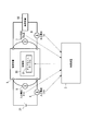
- FIG. 1 is a functional block diagram showing a schematic configuration of the power supply device 1 and the inspection device 2 (dead time setting unit) according to the first embodiment of the present invention.
- the power supply device 1 is a DC / DC converter that converts an input DC voltage into a predetermined DC voltage and outputs the DC voltage, and only the portion directly related to the present invention is shown.
- the power supply device 1 and the inspection device 2 shown in FIG. 1 utilize the fact that the surge voltage generated in the switching element changes when the dead time of the switching element in the synchronous rectifier circuit 60 of the power supply device 1 is changed.
- the inspection device 2 instructs the power supply device 1 to change the dead time of the switching element, and measures the change of the surge voltage according to the change of the dead time.
- the inspection device 2 determines the dead time when the surge voltage is minimized based on the measurement result as the optimum dead time, and notifies the power supply device 1 of information on the optimum dead time.
- the power supply device 1 sets the optimum dead time notified from the inspection device 2 in the storage unit 30.
- the power supply device 1 includes a processing unit 10, a drive circuit 11, a storage unit 30, a synchronous rectification circuit 60, and a surge voltage detection circuit 63. Further, an inspection device 2 for setting input / output currents and input / output voltages in the power supply device 1 is connected to the power supply device 1.
- the processing unit 10 is a control device that controls the overall operation of the power supply device 1.
- the processing unit 10 includes a CPU (Central Processing Unit), a ROM (Read Only Memory), a RAM (Random Access Memory), an A / D converter (ADC; analog-digital converter), a counter, and the like. It includes a microcomputer, a microcontroller, and a DSP (Digital Signal Processor).
- the processing unit 10 may be realized by dedicated hardware.
- the processing unit 10 includes a control unit 101, an acquisition unit 102, a rewriting unit 103, and a transmission unit 104 (details will be described later).
- the drive circuit 11 generates gate signals G5 and G6 for driving the switching elements Q5 and Q6 included in the synchronous rectification circuit 60 from the on / off control signal CNT output from the control unit 101.
- the synchronous rectifier circuit 60 is a synchronous rectifier circuit that performs full-wave rectification on the voltage induced in the secondary winding of the transformer 50 using two switching elements Q5 and Q6. Will be described later).
- the surge voltage detection circuit 63 detects a surge voltage that is generated when the switching elements Q5 and Q6 of the synchronous rectification circuit 60 are turned on and off. The detected value of the surge voltage is transmitted to the inspection device 2 via the transmission unit 104 of the processing unit 10.
- the storage unit 30 stores the dead time (first dead time) of the switching elements Q5 and Q6 that perform synchronous rectification in association with the output current value. For example, as shown in FIG. 7 to be described later, the storage unit 30 stores dead time data associated with the value of the output current Io of the power supply device 1 in the form of a dead time table 31.
- the control unit 101 generates an on / off control signal CNT for controlling the switching operation of the switching elements Q5 and Q6 in the synchronous rectifier circuit 60.
- the on / off control signal CNT is converted by the drive circuit 11 into gate signals G5 and G6 for driving the switching elements Q5 and Q6.
- the control unit 101 refers to the dead time table 31 stored in the storage unit 30 so that the dead time is included in the gate signals G5 and G6. Is generated.
- the acquisition unit 102 receives information on a dead time change instruction from the inspection apparatus 2.
- This change instruction includes information indicating a new dead time after the change.
- the acquisition unit 102 notifies the rewriting unit 103 of the dead time change instruction information received from the inspection apparatus 2.
- the rewriting unit 103 uses the dead time (first dead time) stored in the storage unit 30 based on the dead time change instruction obtained from the obtaining unit 102 as the optimum dead time (second deadline) obtained by the obtaining unit 102. (Dead time). For example, the rewrite unit 103 rewrites the data so as to increase or decrease the already recorded dead time based on the dead time change instruction. Further, when the inspection device 2 determines the optimum dead time, the rewrite unit 103 obtains the optimum dead time via the obtaining unit 102 and rewrites the dead time table 31 with the data of the optimum dead time.
- the transmission unit 104 transmits information indicating the surge voltage values of the switching elements Q5 and Q6 detected by the surge voltage detection circuit 63 to the inspection device 2.
- the inspection apparatus 2 includes an acquisition unit 201, a measurement unit 202, a determination unit 203, a writing unit 204, and a storage unit 205.
- the inspection device 2 is a tester, for example.
- the acquisition unit 201 acquires information indicating the surge voltage value detected by the surge voltage detection circuit 63 transmitted by the processing unit 10.
- the measurement unit 202 measures the magnitude of the surge voltage generated in the switching elements Q5 and Q6 of the synchronous rectification circuit 60 based on the information on the detected value of the surge voltage acquired by the acquisition unit 102.
- the measuring unit 202 instructs the processing unit 10 of the power supply device 1 to change the dead time in the switching elements Q5 and Q6 of the synchronous rectifier circuit 60.
- the determination unit 203 determines, based on the surge voltage value that changes according to the change in the dead time in the synchronous rectification circuit 60, the dead time when the surge voltage is minimized as the optimum dead time.
- the writing unit 204 transmits information on the optimum dead time determined by the determining unit 203 to the acquiring unit 102 of the power supply device 1.
- the dead time table 31 stored in the storage unit 30 of the power supply device 1 may be stored in advance. Further, the inspection apparatus 2 may read the data of the dead time table 31 stored in the storage unit 30 and store the read data of the dead time table 31.
- the inspection device 2 measures the surge voltage when the dead time of the switching element of the synchronous rectifier circuit 60 is changed by the power supply device 1. Thereby, the power supply device 1 can set the dead time when the surge voltage is minimized to the storage unit 30 as the optimum dead time.
- FIG. 2 is an explanatory diagram showing an outline of the setting operation of the optimum dead time.
- a voltmeter 5 that measures the input voltage Vin and an ammeter 6 that measures the input current Iin are arranged on the input side of the power supply device 1.
- a voltmeter 7 for measuring the output voltage Vout and an ammeter 8 for measuring the output current Io are connected to the output side of the power supply device 1.
- the inspection apparatus 2 sets the input voltage Vin, the output current Io, and the output voltage Vout to be constant. That is, the inspection apparatus 2 puts the power supply apparatus 1 in a state where there is no influence of input / output voltage fluctuations or load fluctuations.
- the inspection apparatus 2 instructs the power supply apparatus 1 to change the dead time stored in the dead time table 31 in the storage unit 30 from the reference dead time to an increasing direction and a decreasing direction.
- the change in surge voltage corresponding to the change in dead time is measured.
- the change in surge voltage is measured by changing the dead time from the reference dead time to ⁇ 3 ⁇ T.
- ⁇ T is a time based on the clock signal.
- the reference dead time is a dead time stored in advance in the dead time table 31 before the adjustment of the dead time is started.
- the reference dead time is set in consideration of variations in delay times of the drive circuits 11 of the plurality of power supply devices 1 and variations in characteristics of the switching elements Q5 and Q6.
- This reference dead time is a dead time estimated to be an optimum dead time based on an average dead time.
- the inspection apparatus 2 determines a dead time at which the surge voltage is minimized. That is, the inspection apparatus 2 determines that the dead time with the smallest surge voltage is the optimum dead time. In this procedure, the inspection device 2 notifies the power supply device 1 of information on the optimum dead time, and the power supply device 1 overwrites the dead time table 31 with the optimum dead time corresponding to the current output current Io. Then, the inspection apparatus 2 changes the output current Io to several different current values, repeatedly executes the second procedure and the third procedure, and according to each current value Io, the dead time table The dead time data stored in 31 is corrected to the optimum dead time.
- the amount by which the reference dead time is corrected by the optimum dead time tends to be the same for different values of the output current Io.
- the same tendency means that when the optimum dead time is a value that is changed in the positive direction with respect to the reference dead time at the first output current Io, the optimum dead time at other output currents Io is It tends to be a value changed in the positive direction with respect to the reference dead time.
- the entire dead time data stored in the dead time table 31 may be corrected by the correction amount obtained from one output current Io.
- the inspection device 2 can optimize the dead time by determining the optimum dead time that minimizes the surge voltage and overwriting the determined optimum dead time in the storage unit 30 of the power supply device 1. it can.
- the power supply device 1 of this embodiment sets the optimal dead time for each product individually without adding a measurement circuit for measuring the dead time or a circuit for determining the dead time to the inside of the product. can do.
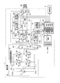
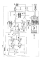
- FIG. 3 is a configuration diagram illustrating a configuration example of the power supply device 1.
- the power supply device 1 shown in FIG. 3 is a DC / DC converter that converts the DC voltage Vin input from the DC power supply 21 into a DC voltage Vout having a predetermined constant voltage.
- the power supply device 1 includes a primary side circuit 40, a synchronous rectification circuit 60, a current detection circuit 70, a processing unit 10, and a drive circuit 11.
- the power supply device 1 is configured to insulate between a primary side circuit and a secondary side circuit by a transformer 50, and a primary winding 51 of the transformer 50 is a full bridge circuit that drives the primary winding 51. 20 is connected.
- a load device 80 is connected to the power supply device 1.
- the primary side circuit 40 includes a primary winding 51 of a transformer 50, a primary winding 55 of a current detection transformer 54, a full bridge circuit 20, a capacitor C1, and a DC power source 21.
- the full bridge circuit 20 is a bridge circuit that drives the primary winding 51, and includes, for example, four switching elements using MOSFET (Metal Oxide Semiconductor Effect Transistor), that is, a switching element Q1, a switching element Q2, a switching element Q3, And a switching element Q4.
- Body diodes D1 to D4 are connected in parallel to the switching elements Q1 to Q4, respectively.
- each of the switching elements Q1 to Q4 has body diodes D1 to D4 (hereinafter referred to as “body diodes”) each having a cathode terminal connected to the drain side and an anode terminal connected to the source side. ).
- each of the switching elements Q1 to Q4 includes body diodes D1 to D4 having cathodes of corresponding diodes D1 to D4 connected to the drain side and anode terminals connected to the source side.
- the drains of the switching elements Q1 and Q3 on the current supply side are connected to the power supply line Vin + on the positive voltage side of the DC power supply 21, and the switching elements Q2 and Q4 on the current supply side are connected.
- the source is connected to the power supply line Vin ⁇ on the negative voltage side of the DC power supply 21.
- the DC power source 21 is connected in parallel with a noise absorbing capacitor C1.
- One terminal a of the primary winding 51 of the transformer 50 is connected to a connection point between the source of the switching element Q1 and the drain of the switching element Q2.
- a connection point between the source of the switching element Q3 and the drain of the switching element Q4 is connected to one terminal k of the primary winding 55 of the current detection transformer 54, and the primary winding 55 of the current detection transformer 54
- the other terminal g is connected to the other terminal b of the primary winding 51 of the transformer 50.
- Signals G1 to G4 are supplied from the processing unit 10 via the drive circuit 11 to the gates of the switching elements Q1 to Q4, respectively. Thereby, the power supply device 1 can drive the primary winding 51 of the transformer 50 by the full bridge circuit 20 and measure the current flowing through the primary winding 51 by the current detection transformer 54.
- the full bridge circuit 20 is configured to turn on / off the switching elements Q1 to Q4 based on the leakage inductance (leakage inductance) of the primary winding 51 of the transformer 50 and the capacitors component (parasitic capacitance) of the switching elements Q1 to Q4. It is configured as a partial resonance type full bridge circuit that uses the resonance action only in the transient state of time. That is, the control unit 101 turns on the switching elements Q1 and Q4 or the switching elements Q2 and Q3 at a timing when the charge accumulated in the parasitic capacitances of the switching elements Q1 to Q4 becomes as small as possible. The switching loss in Q4 is reduced. Note that the capacitors component in the switching elements Q1 to Q4 is the sum of the capacitance between the drain and the source and the capacitance between the gate and the drain.
- the gate signals G1 to G4 output from the drive circuit 11 are supplied to the gates of the switching elements Q1 to Q4 in the full bridge circuit 20, respectively. Thereby, switching elements Q1 to Q4 are controlled to be in an on state and an off state.
- the gate signals G1 to G4 are signals generated based on the on / off control signal CNT (PWM signal) output from the control unit 101 in the processing unit 10.
- the drive circuit 11 also generates gate signals G5 and G6 for controlling switching elements Q5 and Q6 in a synchronous rectification switch circuit 61, which will be described later, to an on state and an off state.
- the gate signals G5 and G6 are signals generated based on the on / off control signal CNT output from the control unit 101 in the processing unit 10.
- the drive circuit 11 controls the switching elements Q1 to Q4 to be in an on state and an off state
- the drive circuit 11 has a period in which the switching elements Q1 and Q4 are in an on state and the switching elements Q2 and Q3 are in an off state
- a gate signal is generated in which Q4 is in an off state and switching elements Q2 and Q3 are in an on state alternately.
- a current flows from one end of the primary winding 51 of the transformer 50 toward the other end, and a current flows from the other end of the primary winding 51 toward the one end.
- induced voltages V1 and V2 are generated in the secondary windings 52 and 53 of the transformer 50.
- the primary side circuit 40 is provided with a first current detection circuit 22 for measuring a current flowing through the full bridge circuit 20 via the power supply line Vin +.
- the first current detection circuit 22 is a current detection circuit for preventing overcurrent protection of the switching elements Q1 to Q4. Based on the detection result of the first current detection circuit 22, the processing unit 10 detects that an overcurrent of a predetermined value or more has flowed through the full bridge circuit 20 via the power line Vin +. To instruct the drive circuit 11 to immediately turn off Q4 to prevent the switching elements Q1 to Q4 from being destroyed by an overcurrent.
- the full bridge circuit 20 of the primary side circuit 40 is connected to the primary winding 51 of the transformer 50 and the primary winding 55 of the current detection transformer 54.
- a synchronous rectifier circuit 60 for full-wave rectifying the voltage induced in the secondary windings 52 and 53 is connected to the secondary windings 52 and 53 of the transformer 50.
- a current detection circuit 70 is connected to the secondary winding 56 of the current detection transformer 54.
- the synchronous rectifier circuit 60 includes secondary windings 52 and 53 of the transformer 50, a synchronous rectification switch circuit 61, a rectification smoothing circuit (choke coil L11 and capacitor C11), a second current detection circuit 62, and a surge voltage detection circuit 63.
- the synchronous rectifier circuit 60 performs full-wave rectification on the voltages V1 and V2 (inductive electromotive force) induced in the secondary windings 52 and 53 of the transformer 50 and converts the voltages into DC voltages.
- the switching elements Q5 and Q6 constituting the synchronous rectifier switch circuit 61 are controlled by the control unit 101 to be turned on and off, and induced in the secondary windings 52 and 53 of the transformer 50.
- the voltages V1 and V2 are synchronously rectified.
- the synchronous rectification circuit 60 smoothes the synchronously rectified DC voltage with the choke coil L11 and the capacitor C11, and supplies power to the load device 80 via the output terminals Out1 and Out2.
- the load device 80 is, for example, a lamp, a motor, a battery, or the like.
- the switching elements Q5 and Q6 of the synchronous rectification switch circuit 61 are constituted by MOSFETs, for example.
- Body diodes D5 and D6 are connected in parallel to switching elements Q5 and Q6, respectively. That is, each of the switching elements Q5 and Q6 is connected to the cathode terminals of the diodes D5 and D6 corresponding to the drain side and to the anode terminal on the source side.
- the center tap of the secondary winding of the transformer 50 that is, the terminal d of the connection point of the secondary winding 52 and the secondary winding 53 is connected to one end of the choke coil L11, and the choke coil The other end of L11 is connected to the positive voltage side electrode of the capacitor C11 and to the positive voltage side output terminal Out1.
- the drain of the switching element Q6 in the synchronous rectification switch circuit 61 is connected to the terminal c of the secondary winding 52 of the transformer 50.
- the source of the switching element Q6 is connected to the reference potential side via the reference potential line GND. Are connected to the output terminal Out2.
- the drain of the switching element Q5 in the synchronous rectification switch circuit 61 is connected to the terminal e of the secondary winding 53 of the transformer 50.
- the source of the switching element Q5 is connected to the output terminal Out2 via the reference potential line GND. It is connected.
- the processing unit 10 controls the timing of the ON state and the OFF state of the switching elements Q5 and Q6 in synchronization with the timing at which the voltages V2 and V3 are induced in the secondary windings 52 and 53 of the transformer 50. To do. As described above, by controlling the switching elements Q5 and Q6 between the on state and the off state, it is possible to reduce the power loss caused by the forward voltage Vf of the diodes D5 and D6.
- the synchronous rectifier circuit 60 is provided with a second current detection circuit 62 for measuring a current flowing through the switching element Q5 (or both of the switching elements Q5 and Q6).
- the second current detection circuit 62 outputs a signal indicating the current flowing through the measured switching element Q5 (or both of the switching elements Q5 and Q6) to the processing unit 10.
- the synchronous rectifier circuit 60 is provided with a surge voltage detection circuit 63 for detecting a surge voltage generated at the drain terminals of the switching elements Q5 and Q6.
- the surge voltage detection circuit 63 is constituted by a peak value hold circuit, for example, and outputs a detection signal of the detected surge voltage to the processing unit 10.
- the current detection circuit 70 includes a secondary winding 56 of a current detection transformer 54, a rectifier circuit 71, a diode 72, a voltage dividing circuit 73, and a third current detection circuit 74.
- the primary winding 51 and the secondary windings 52 and 53 constitute a transformer 50
- the primary winding 55 and the secondary winding 56 constitute a current detection transformer 54.
- the output current Io is indirectly detected by detecting the current flowing through the primary winding 51 of the transformer 50 using the current detection transformer 54 and the current detection circuit 70. It is configured. This is because when a current detection transformer is inserted in series with the choke coil L11 of the synchronous rectifier circuit 60 to detect the output current Io, for example, when an output current Io exceeding 100 A is detected, Noise may be superimposed on the detected value of the transformer, and a problem of heat generation may occur. Therefore, the output current Io is detected by detecting the primary current flowing in the primary winding 51 of the transformer 50 with the current detecting transformer 54. Of course, as will be described later, the output current Io may be detected in the synchronous rectifier circuit 60.
- the current detection circuit 70 includes a rectifier circuit 71 connected to the terminals m and n of the secondary winding 56 of the current detection transformer 54, a diode 72, a voltage dividing circuit 73, and a third current detection circuit 74. is doing.
- the anode of the diode 72 is connected to one terminal of the rectifier circuit 71, and the cathode is connected to the voltage dividing circuit 73.
- the voltage dividing circuit 73 outputs a signal S1 representing the divided result to the processing unit 10.
- One end of the third current detection circuit 74 is connected to one terminal of the rectifier circuit 71, and outputs a signal S2 representing the detection result to the processing unit 10.
- the rectifier circuit 71 is a full-wave rectifier circuit configured by a diode bridge circuit.
- the voltage dividing circuit 73 is configured by a resistance voltage dividing circuit.
- a circuit composed of the diode 72 and the voltage dividing circuit 73 forms a return loop of the current Ict output from the rectifier circuit 71.
- the signal S1 output from the voltage dividing circuit 73 to the processing unit 10 can be used as, for example, a signal for overcurrent protection of the switching elements Q1 to Q4.
- the diode 72 is a voltage compensation diode for compensating for Vf (a forward voltage drop) generated in a diode 741 of a third current detection circuit 74 described later.
- the third current detection circuit 74 is a circuit for indirectly detecting the output current Io from the current Ict output from the secondary winding 56 of the current detection transformer 54 via the rectifier circuit 71.
- FIG. 4A is a configuration diagram illustrating a configuration example of the third current detection circuit 74.
- the third current detection circuit 74 includes a capacitor 742 that is charged by a current Ict through a diode 741, and resistors 743 and 744 for voltage division for detecting the voltage across the capacitor 742. And a noise absorbing capacitor 745 and a resistor 746.
- the anode of the diode 741 is an input terminal of the third current detection circuit 74.
- the cathode of the diode 741 is connected to one end of the resistor 743 and one end of the capacitor 742.
- the diode 741 serves to detect a current peak.
- the other end of the resistor 743 is connected to one end of the resistor 744, one end of the capacitor 745, and one end of the resistor 746.
- the other end of the capacitor 742, the other end of the resistor 744, and the other end of the capacitor 745 are grounded.
- the capacitor 742, the capacitor 745, the resistor 743, the resistor 744, and the resistor 746 constitute a circuit that detects current at a desired response speed.
- the other end of the resistor 746 is connected to the ADC 110 of the processing unit 10.
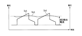
- FIG. 4B is a waveform diagram for explaining the operation of the third current detection circuit 74.
- the horizontal axis represents time
- the vertical axis represents voltage and current.
- the capacitor 742 of the third current detection circuit 74 is caused by the current Ict. Charged.
- the voltage Vct across the capacitor 742 charged by this current Ict has a smoothed voltage waveform as shown in FIG. 4B.
- This voltage Vct is divided by resistors 743 and 744, and a connection point N 1 between the resistors 744 and 743 conforms to an input voltage range of the A / D converter (ADC) 110 in the processing unit 10.
- a voltage signal Vsc is generated.
- the resistor 744 is connected with a noise absorbing capacitor 745 in parallel.
- the voltage signal Vsc is input to the A / D converter 110 in the processing unit 10 as the signal S2 via the resistor 740.
- the A / D converter 110 performs A / D conversion on the signal S ⁇ b> 2 and inputs a digital value signal obtained by the A / D conversion to the control unit 101.
- the current detection circuit 70 can indirectly detect the output current Io by detecting the current flowing through the primary winding 51 of the transformer 50.
- the control unit 101 in the processing unit 10 supplies the gate signals G1 to G4 to the switching elements Q1 to Q4 in the full bridge circuit 20 via the drive circuit 11, respectively. That is, the control unit 101 detects the output voltage Vout by an output voltage detection circuit (not shown), and sets the ON / OFF timing (duty ratio) of the switching elements Q1 to Q4 so that the output voltage Vout becomes constant. Control. In addition, the control unit 101 supplies gate signals G5 and G6 to the switching elements Q5 and Q6 in the synchronous rectification switch circuit 61 via the drive circuit 11, respectively. That is, the control unit 101 controls the switching elements Q5 and Q6 to turn on / off, thereby causing the switching elements Q5 and Q6 to perform synchronous rectification.
- FIG. 5 is a time chart showing the waveforms of the gate signals of the switching elements Q5 and Q6.
- the horizontal axis indicates time t
- the vertical axis indicates the voltage waveform induced in the secondary windings 52 and 53 by the current flowing through the primary winding 51 of the transformer 50
- the waveform of the gate signal G6 of the switching element Q6 are shown side by side.
- FIG. 5 is an explanatory diagram showing a mode of current flowing in the synchronous rectifier circuit and a mode of current in the dead time. For example, as shown in the upper part of FIG. 6, it is assumed that the current I1 is flowing back to the secondary winding 53 of the transformer 50 via the switching element Q5 at the time t0.
- the control unit 101 sets the gate signal G5 to L and turns off the switching element Q5.
- the gate signal G6 is H, and the switching element Q6 remains on.
- the switching elements Q2 and Q3 of the full bridge circuit 20 are turned on.
- a negative voltage is induced in the secondary windings 52 and 53 of the transformer 50.
- the negative voltage means that the potential of the terminal e of the secondary windings 52 and 53 is higher than the potential of the terminal c.
- the ON state of the switching elements Q2 and Q3 of the full bridge circuit 20 is continued until time t3.
- the switching element Q5 is turned on at time t4 when a predetermined dead time DT25 has elapsed. Note that the switching element Q6 remains on. In this dead time DT25, since the mode of the current flowing through the switching elements Q5 and Q6 does not change, no surge voltage is generated in the dead time DT25.
- the control unit 101 sets the gate signal G6 to L and turns off the switching element Q6.
- the gate signal G5 is H, and the switching element Q5 remains on.
- the switching element Q6 is turned off at time t5
- the current that has been flowing through the switching element Q6 so far is commutated to the body diode D6.
- the switching elements Q1 and Q4 of the full bridge circuit 20 are turned on.
- a positive voltage is applied to secondary windings 52 and 53 of transformer 50.
- the positive voltage means that the potential of the terminal c of the secondary windings 52 and 53 is higher than the potential of the terminal e. Then, in the dead time DT46 from time t5 to time t6, when the switching element Q6 is turned off, the mode of the current flowing through the switching element Q6 changes in the same manner as when the switching element Q5 is turned off. Therefore, a large surge voltage is generated at the drain terminal of the switching element Q6.
- the switching element Q6 is turned on at time t8 when a predetermined dead time DT16 has elapsed. Note that the switching element Q5 remains on. In this dead time DT16, since the mode of the current flowing through the switching elements Q5 and Q6 does not change, no surge voltage is generated in the dead time DT16. Subsequent operations after time t8 are the same as the operations after time t1 described above.
- FIG. 7 is an explanatory diagram showing an example of the dead time table 31 stored in the storage unit 30.
- the storage unit 30 stores dead time data in the form of a table. That is, the dead time DT16, the dead time DT25, the dead time DT46, and the dead time DT35, which are used when controlling the switching elements Q5 and Q6 constituting the synchronous rectifier circuit 60 to the on state and the off state, It is stored in the form of a table in association with the output current Io of the device 1.
- the control unit 101 sets the dead time according to the magnitude of the output current Io of the power supply device 1 with reference to the dead time table 31 shown in FIG.
- the control unit 101 selects the dead time dt3 as the dead time DT16 and the dead time DT25, and selects the dead time dt13 as the dead time DT46 and the dead time DT35. Then, when generating the gate signals G5 and G6 illustrated in FIG. 5, the control unit 101 generates the gate signals G5 and G6 using the dead time dt3 and the dead time dt13.
- the dead time table 31 is stored in an EEPROM (Electrically Erasable Programmable Read-Only Memory) in the storage unit 30.
- the initial value data of the dead time stored in the dead time table 31 corresponds to, for example, the average value of the variation in delay time of the drive circuit 11 and the average value of the variation in characteristics of the switching elements Q4 and Q5.
- a value estimated as the optimum dead time can be used.
- This initial value data is a value set for each output current value zero (0), Io1, Io2, Io3, Io4, Io5, and Io6. That is, the initial value data stored in the dead time table 31 is the optimum dead time when the delay time of the drive circuit 11 and the characteristics of the switching elements Q4 and Q5 coincide with the average value.
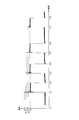
- FIG. 8 is a waveform diagram showing an example of the drain-source voltage Vds of the switching element when the dead time is changed.
- This waveform diagram is an example of the waveform of the drain-source voltage Vds of the switching element Q5, for example.
- the horizontal axis represents time
- the vertical axis represents voltage.
- surge voltages V 1 to V 4 are generated. To do.
- the peak values of the surge voltages V 1 to V 4 change.
- the waveforms at times t11 to t12 are waveforms when the dead time is set to DT-3, that is, “reference dead time ⁇ 3 ⁇ ⁇ T”.
- the peak value of the surge voltage is V 1.
- ⁇ T is a predetermined unit time ⁇ T.
- the waveforms at times t13 to t14 are waveforms when the dead time is set to DT-2, that is, “reference dead time ⁇ 2 ⁇ ⁇ T”.
- the peak value of the surge voltage is V 2.
- the waveforms at times t15 to t16 are waveforms when the dead time is set to DT-1, that is, “reference dead time ⁇ 1 ⁇ ⁇ T”.
- the peak value of the surge voltage is V 3.
- the waveforms at times t17 to t18 are waveforms when the dead time is set to DT, that is, “reference dead time”.
- the peak value of the surge voltage is V 4.
- the voltage value V 1 was higher than the voltage value V 2
- the voltage value V 2 is higher than the voltage value V 3
- the voltage value V 3 is higher than the voltage value V 4. That is, in the example shown in FIG. 8, the peak value of the surge voltage is the highest when the dead time is DT-3, and the peak value of the surge voltage is the lowest when the dead time is DT.
- FIG. 9 is an explanatory diagram showing a measurement example of the surge voltage when the dead time is changed.
- the reference dead time reference dead time
- the predetermined time ⁇ T is changed as a unit time.
- the dead time is changed from the reference dead time in the + direction to +3 (reference dead time + 3 ⁇ ⁇ T), and is changed in the ⁇ direction to ⁇ 3 (reference dead time ⁇ 3 ⁇ ⁇ T). I am letting.
- the inspection apparatus 2 measures the surge voltage e which changes according to the time width of dead time.
- the dead time is “0 (reference dead time)”
- the surge voltage is the smallest
- the dead time is “ ⁇ 3 (reference dead time ⁇ 3 ⁇ ⁇ T)”
- the surge voltage becomes the largest.
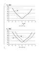
- FIG. 10 is a graph showing an example of a change in surge voltage when the dead time is changed and a change in surge voltage due to variations in the characteristics of the switching elements.
- the upper part of FIG. 10 is a graph showing the change of the surge voltage when the dead time is changed, and is a graph showing the measurement result of the surge voltage e shown in FIG.
- the horizontal axis represents the change in dead time
- the vertical axis represents the surge voltage level.
- the reference dead time is set to 0, and the surge voltage changes when the reference dead time is changed in the + direction and the ⁇ direction with a predetermined time ⁇ T as a unit time. The characteristics are shown.
- reference symbols e1 to e9 indicate surge voltage levels.
- the surge voltage e changes.
- the dead time is zero (0), that is, the dead time becomes the reference dead time.
- the surge voltage is minimized.
- the characteristics of the surge voltage corresponding to the dead time vary depending on the delay time of the drive circuit 11 and variations in the characteristics of the switching elements Q5 and Q6.
- the surge voltage may be minimized when the dead time is +1 (reference dead time + ⁇ T) due to variations in the characteristics of the switching elements.
- the inspection apparatus 2 determines that the dead time of “reference dead time + ⁇ T” is the optimum dead time that minimizes the surge voltage e, and the output to which this optimum dead time is applied.
- the power supply device 1 is notified of the current value information.
- the power supply device 1 rewrites the dead time table 31 in the storage unit 30 with the data of the optimum dead time based on the information of the optimum dead time and output current value received from the inspection device 2.
- the dead time includes four types of dead time, that is, dead time DT35, dead time DT25, dead time DT46, and dead time DT16.
- the dead time DT25 and the dead time DT16 are irrelevant to the generation of the surge voltage. Therefore, the inspection apparatus 2 determines the optimum dead time for each of the dead time DT35 and the dead time DT46.
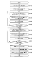
- FIG. 11 is a flowchart showing the flow of the optimum dead time setting process, and shows the flow of the optimum dead time setting process in the power supply device 1 and the inspection device 2 described above.
- the optimal dead time setting process is performed for the dead time DT35 and the dead time DT46.
- the optimal dead time may be set in any order, for example, after the dead time DT35 is set.
- the dead time DT46 can be set.
- a voltmeter 5 that measures the input voltage Vin and an ammeter 6 that measures the input current Iin are arranged in advance on the input side of the power supply device 1, and the output of the power supply device 1 It is assumed that a voltmeter 7 for measuring the output voltage Vout and an ammeter 8 for measuring the output current Io are arranged in advance on the side.
- the power supply device 1 and the inspection device 2 set the input voltage Vin, the output voltage Vout, and the output current Io to be constant (step S110).
- an electronic load device is used as the load device 80 so that the output current Io is constant.
- the control unit 101 of the power supply device 1 reads the dead time corresponding to the output current Io from the dead time table 31 and generates gate signals G5 and G6 via the drive circuit 11. Note that at the start of the optimum dead time setting process, the dead time becomes the reference dead time.
- the inspection device 2 acquires the data of the detected value of the surge voltage detected by the surge voltage detection circuit 63 in the power supply device 1 from the transmission unit 104 of the processing unit 10 during the reference dead time.
- the inspection device 2 measures the magnitude of the surge voltage generated in the switching element of the synchronous rectifier circuit 60 based on the data of the detected value of the surge voltage acquired from the processing unit 10 (step S120).
- the inspection device 2 stores the surge voltage measurement data in the storage unit 205.
- the inspection apparatus 2 instructs the power supply apparatus 1 to increase the current dead time by +1 ( ⁇ T increase) in the increasing direction of the current dead time (step S130).
- the dead time is “reference dead time + 1 ⁇ ⁇ T”.
- the power supply device 1 stores a new dead time obtained by adding +1 ( ⁇ T increase) to the current dead time in the dead time table 31, and changes the dead time.
- the power supply device 1 generates the gate signals G5 and G6 based on the changed dead time, and drives the switching elements Q5 and Q6 (step S140).
- the inspection device 2 obtains data of the detected value of the surge voltage detected by the surge voltage detecting circuit 63 from the processing unit 10 and is generated in the switching element of the synchronous rectifier circuit 60 based on the data of the detected value.
- the magnitude of the surge voltage to be measured is measured (step S150).
- the inspection device 2 stores the surge voltage measurement data in the storage unit 205.
- the inspection apparatus 2 determines whether or not the dead time has been changed to +3 (reference dead time + 3 ⁇ ⁇ T) (step S160). If it is determined in the determination process in step S160 that the dead time has not been changed to +3 (step S160: NO), the inspection apparatus 2 returns to the process in step S130 to change the dead time and the surge voltage. The measurement process is continued.
- step S160 when it is determined that the dead time has been changed to +3 (step S160: YES), the inspection apparatus 2 proceeds to the process of step S170. Then, the inspection device 2 sets the dead time to 1 (step S170). Further, when it is determined in step S200 that it is not -3, the inspection apparatus 2 subtracts the dead time by -1. For example, when the dead time is -1, the dead time becomes -2 by this process. Subsequently, the power supply device 1 stores the dead time set to ⁇ 1 or the dead time obtained by subtracting 1 in the dead time table 31 to change the dead time. The power supply device 1 generates the gate signals G5 and G6 based on the changed dead time, and drives the switching elements Q5 and Q6 (step S180).
- the inspection device 2 obtains data of the detected value of the surge voltage detected by the surge voltage detecting circuit 63 from the processing unit 10 and is generated in the switching element of the synchronous rectifier circuit 60 based on the data of the detected value. Measure the surge voltage level.
- the inspection device 2 stores the measurement data of the surge voltage in the storage unit 205 (step S190).
- the inspection apparatus 2 determines whether or not the dead time has been changed to ⁇ 3 (reference dead time ⁇ 3 ⁇ ⁇ T) (step S200). If it is determined in the determination process of step S200 that the dead time has not been changed to -3 (step S200: NO), the inspection apparatus 2 returns to the process of step S170 to change the dead time, Continue the voltage measurement process.
- step S200 when it is determined that the dead time has been changed to ⁇ 3 (step S200: YES), the inspection apparatus 2 proceeds to the process of step S210. Then, the inspection device 2 determines the dead time at which the surge voltage is minimized based on the measured data of the surge voltage measured by changing the dead time in the ⁇ 3 direction from the reference dead time. That is, the inspection apparatus 2 determines that the dead time with the smallest surge voltage is the optimum dead time (step S210). Subsequently, the inspection apparatus 2 notifies the power supply apparatus 1 of information on the optimum dead time (step S220).
- the power supply device 1 writes the optimum dead time notified from the inspection device 2 in the dead time table 31 in the storage unit 30 (step S230). Then, after executing the process of step S230, the power supply apparatus 1 and the inspection apparatus 2 finish the setting process of the optimum dead time of the PCS 40.
- the inspection device 2 repeatedly performs the processing from step S110 to S230 for several different output currents Io, determines the optimum dead time according to each current value, and notifies the power supply device 1 of the determination. To do.
- the power supply device 1 sets the optimum dead time in the dead time table 31 by writing the optimum dead time acquired from the inspection device 2 into the dead time table 31.
- the dead time is determined when determining the dead time corresponding to the first output current Io to be measured.
- the output current Io is indirectly measured by detecting the current flowing through the primary winding 51 of the transformer 50 using the current detection transformer 54 and the current detection circuit 70. ing.
- the output current Io may be detected by providing a current detection circuit in the synchronous rectification circuit 60.
- FIG. 12 is a configuration diagram showing a configuration example of the power supply device 1A according to the second embodiment of the present invention.
- the power supply device 1A shown in FIG. 11 excludes the current detection transformer 54 and the current detection circuit 70 on the primary winding 51 side shown in FIG.
- the point that the current detection transformer 64 and the output current detection circuit 65 are newly added in the synchronous rectification circuit 60 is different in configuration.
- the configuration differs in that the first current detection circuit 22 and the second current detection circuit 62 shown in FIG. 3 are omitted.
- Other configurations are the same as those of the power supply device 1 shown in FIG. For this reason, the same code
- a current detection transformer 64 is inserted between the choke coil L11 and the output terminal Out1, and the output current Io flowing from the power supply device 1A to the load device 80 by the current detection transformer 64. Is detected.
- an output current detection circuit 65 for detecting a current value of the output current Io is formed while a circulation loop of a current flowing in the secondary winding side is formed.
- the output current detection circuit 65 includes a circuit similar to the third current detection circuit 74 shown in FIG. 4, and the current signal Is detected by the output current detection circuit 65 is sent to the processing unit 10. Entered.
- the optimum dead time setting operation for minimizing the surge voltage in the power supply device 1A is the first embodiment except that the output current Io is detected by the current detection transformer 64 in the synchronous rectifier circuit 60. This is performed in the same manner as the power supply device 1 of FIG. For this reason, the overlapping description is omitted.
- the optimum dead time can be set according to the value of the output current Io by directly detecting the output current Io flowing from the output terminal Out1 to the load device 80. .
- the primary winding 51 of the transformer 50 is driven by the full bridge circuit 20 .
- the primary winding 51 of the transformer 50 is a half bridge circuit. This can also be applied to the case of driving with.
- FIG. 13 is a configuration diagram showing a configuration example of a power supply device 1B according to the third embodiment of the present invention.
- the circuit configuration of the power supply device 1B including the half bridge circuit 20A shown in FIG. 13 is generally well known.
- the half bridge circuit 20A alternately turns on and off the switching elements Q1 and Q2, and drives the primary winding 51 of the transformer 50 by the electric charges accumulated in the capacitors C2 and C3.
- the voltage induced in the secondary windings 52 and 53 is full-wave rectified by the synchronous rectification circuit 60 and supplied to the load device 80 via the choke coil L11.
- the configurations of the synchronous rectification circuit 60 and the current detection circuit 70 are the same as those of the power supply device 1 shown in FIG. 3, and the operations thereof are also the same. For this reason, the overlapping description is omitted.
- the optimum dead time that minimizes the surge voltage can be set in the synchronous rectifier circuit 60.
- the power supply device of the present invention may be a power supply device provided with the synchronous rectification circuit 60 on the secondary windings 52 and 53 side, and the circuit for driving the primary winding 51 of the transformer 50 has any configuration. It may be.
- the power supply device may be a power supply device that drives the primary winding 51 by a feed forward method or a push-pull method.
- the surge voltage is minimized without adding a circuit for determining the optimum dead time of the switching elements Q5 and Q6 to the inside of the product.
- the optimal dead time can be set for each product.
- the power supply device can correct the dead time to the optimum value for each product according to the delay time of the drive circuit and the characteristics of the switching element. For this reason, the power supply device can use a switching element having a low withstand voltage, which contributes to high efficiency.
- the power supply apparatus corresponds to the power supply apparatus 1, the power supply apparatus 1 ⁇ / b> A, or the power supply apparatus 1 ⁇ / b> B.
- the first dead time in the present invention is data stored in the dead time table 31 of the storage unit 30, and corresponds to data of the dead time before being rewritten to the optimum dead time.
- the second dead time corresponds to the optimum dead time determined by the inspection apparatus 2, and the dead time table 31 of the storage unit 30 is finally rewritten to this optimum dead time.
- the switching elements in the present invention correspond to the switching elements Q5 and Q6 in the synchronous rectification switch circuit 61.
- the surge voltage detection circuit 63 corresponds to the detection unit in the present invention.
- the power supply device 1 detects the surge voltage value generated in the storage unit 30 that stores the first dead time of the switching elements Q5 and Q6 that perform synchronous rectification, and the switching elements Q5 and Q6.
- the detection unit (surge voltage detection circuit 63), the transmission unit 104 that outputs information indicating the surge voltage value detected by the detection unit (surge voltage detection circuit 63), and the information indicating the surge voltage value.
- An acquisition unit 201 that acquires information on the second dead time (optimum dead time), a rewriting unit 103 that rewrites the first dead time stored in the storage unit 30 with the second dead time acquired by the acquisition unit 102, and a storage And a control unit 101 that controls the switching elements Q5 and Q6 according to the second dead time stored in the unit 30.
- a surge voltage value generated in the switching elements Q5 and Q6 that perform synchronous rectification is detected, and information indicating the surge voltage value is output to the outside. Further, the power supply apparatus 1 inputs information on the second dead time (optimum dead time) set based on the information indicating the surge voltage value from the outside, and sets the first dead time stored in the storage unit 30 as the first dead time.
- the control unit 101 controls the switching elements Q5 and Q6 according to the second dead time.
- the power supply device 1 has a second dead time (optimum dead time) at which the surge voltage is minimized without adding a circuit for measuring the surge voltage or a new circuit for determining the dead time. Can be set for each product.
- the acquisition unit 201 is a dead time setting unit (inspection apparatus) that inputs information indicating a surge voltage value from the transmission unit 104 when acquiring the second dead time (optimum dead time). 2)
- the information on the second dead time is input from the inspection device 2 that determines the second dead time based on the information indicating the surge voltage value.
- the dead time setting unit inputs information indicating the surge voltage value from the transmission unit 104, and the second dead time based on the information on the surge voltage value. Determine.
- the acquisition unit 102 of the power supply device 1 acquires information on the second dead time from the dead time setting unit (inspection device 2), and stores the second dead time in the storage unit 30.
- the dead time setting unit determines the second dead time (optimum dead time) at which the surge voltage is minimized based on the detected value of the surge voltage, and the power supply device 1
- the dead time information can be acquired from the dead time setting unit (inspection apparatus 2) and stored in the storage unit 30.
- the second dead time (optimum dead time) is a constant of the input voltage Vin to the power supply device 1, the output voltage Vout from the power supply device 1, and the output current Io from the power supply device 1.
- the surge voltage value is the smallest value.
- the power supply device having such a configuration, the dead time is changed while the input voltage Vin to the power supply device 1, the output voltage Vout from the power supply device 1, and the output current Io from the power supply device 1 are kept constant.
- the power supply device 1 acquires information on the dead time when the surge voltage becomes the smallest by the acquisition unit 102 and stores the second dead time (optimum dead time) in the storage unit 30.
- the second dead time (optimum dead time) is determined in a state where there is no influence of input / output voltage fluctuations or load fluctuations, and the power supply device 1 acquires the accurate second dead time (optimum dead time). be able to.
- the storage unit 30 stores the relationship between the output current and the first dead time for each output current, and the rewrite unit 103 is stored in the storage unit 30.
- the first dead time for each output current is rewritten to the second dead time for each output current acquired by the acquisition unit 102.
- the storage unit 30 stores the relationship between the output current and the first dead time for each output current.
- the power supply device 1 acquires the information of the 2nd dead time for every output current by the acquisition part 102, and the output from which the acquisition part 102 acquired the 1st dead time for every output current memorize
- the 2nd dead time (optimal dead time) can be set for every output current by rewriting the 1st dead time memorize
- the inspection device 2 of the present invention provides a power supply device 1 that can change the first dead time of the switching elements (Q5 and Q6) that perform synchronous rectification according to information on dead time that is externally input.
- a measurement unit 202 that inputs information on a detected value of a surge voltage generated in the switching elements (Q5 and Q6) from the power supply device 1 and measures the surge voltage, and a measurement unit 202 Based on the measurement result of the surge voltage measured by the above, the determination unit 203 for determining the second dead time at which the surge voltage becomes the smallest, and the power supply device 1 are notified of the second dead time information.
- a writing unit 204 that sets the first dead time to the second dead time.
- the inspection device 2 having such a configuration instructs the power supply device 1 to change the first dead time of the switching elements (Q5 and Q6) that perform synchronous rectification, and generates a surge voltage generated in the switching element. Measure. Then, the inspection device 2 determines a second dead time (optimum dead time) at which the surge voltage is the smallest based on the measurement result of the surge voltage, and notifies the power supply device 1 of information on the two dead times. The power supply device 1 rewrites the first dead time data stored in the storage unit 30 to the second dead time (optimum dead time).
- the inspection device 2 measures the surge voltage generated in the switching elements (Q5 and Q6) while changing the dead time of the switching elements (Q5 and Q6) that perform synchronous rectification of the power supply device 1, thereby 2 dead time (optimum dead time) can be determined. Then, the inspection device 2 can cause the power supply device 1 to set the second dead time. Therefore, in the power supply device 1, the surge voltage generated in the switching element that performs synchronous rectification is minimized without adding a circuit for measuring the surge voltage or a new circuit for determining the dead time to the inside of the product. Optimal dead time can be set for each product.
- the measurement unit 202 maintains the input voltage to the power supply apparatus 1, the output voltage from the power supply apparatus, and the output current from the power supply apparatus 1 in a constant state.
- the apparatus 1 is instructed to change the first dead time and measures the surge voltage, and the determination unit 203 has the smallest surge voltage based on the measured value of the surge voltage measured by the measurement unit 202.
- the second dead time is determined.
- the inspection apparatus 2 can determine the optimum dead time (second dead time) in a state where there is no influence of fluctuations in the input / output voltage of the power supply apparatus 1 and load fluctuations. For this reason, the power supply device 1 can acquire an accurate second dead time.
- the optimization method of the power supply device 1 of this invention is the power supply which optimizes the dead time of the switching element (Q5 and Q6) which performs synchronous rectification of the power supply device 1 by a dead time setting part (inspection apparatus 2).
- Q6 including a procedure for detecting a surge voltage value generated in Q6) and outputting information indicating the surge voltage value to a dead time setting unit (inspection device 2), wherein the dead time setting unit (inspection device 2)
- the power supply device 1 is instructed to change the first dead time, and information indicating the surge voltage value generated in the switching elements (Q5 and Q6) is acquired from the power supply device 1.
- the dead time setting unit (inspection apparatus 2) measures the magnitude of the surge voltage generated in the switching elements (Q5 and Q6) based on the information on the surge voltage value, and the dead time setting unit (inspection) The apparatus 2) determines the second dead time at which the surge voltage is minimized based on the measured value of the surge voltage, and the dead time setting unit (inspection apparatus 2) uses the second dead time information as the power supply apparatus 1. And in the power supply device 1, a procedure for setting the first dead time to the second dead time is included. With such an optimization method for the power supply device 1, the dead time setting unit (inspection device 2) changes the first dead time for the power supply device 1 that can change the first dead time of the switching element. The surge voltage generated in the switching element of the power supply device 1 is measured.
- the dead time setting unit determines the dead time at which the surge voltage is the smallest as the second dead time (optimal dead time) based on the measurement result of the surge voltage. Then, the dead time setting unit (inspection apparatus 2) notifies the power supply apparatus 1 of the information on the second dead time, and causes the power supply apparatus to set the first dead time to the second dead time. Thereby, the power supply device 1 can set the optimum dead time for which the surge voltage is minimized for each product without adding a circuit for measuring the surge voltage or a new circuit for determining the dead time inside the product. .
- the second dead time is a state in which the input voltage to the power supply device 1, the output voltage from the power supply device 1, and the output current from the power supply device 1 are kept constant.
- the surge voltage value is the smallest value.
- the dead time setting unit (inspection device 2) calculates the input voltage to the power supply device 1, the output voltage from the power supply device 1, and the output current from the power supply device 1. While maintaining a constant value, the surge voltage generated in the switching element is measured while changing the dead time. Then, the dead time setting unit (inspection apparatus 2) determines the dead time when the surge voltage is the smallest as the second dead time (optimum dead time). As a result, the second dead time (optimum dead time) is determined in a state where there is no influence of input / output voltage fluctuations or load fluctuations, and the power supply device 1 acquires the accurate second dead time (optimum dead time). be able to.
- the dead time setting unit (inspection device 2) determines the second dead time for the first output current, the positive / negative direction in which the first dead time is changed And a procedure for determining a second dead time for the second output current based on the information indicating.
- the dead time setting unit (inspection device 2) is the first measurement target when the dead time is corrected for several different output currents.
- the dead time corresponding to the output current is determined, it is stored which of the positive and negative directions the surge voltage is minimized when the dead time is changed.
- the dead time setting unit determines the dead time for the second output current, The dead time is changed from the positive direction, the surge voltage starts to increase, and the dead time adjustment is finished when it is detected that the bottom point is reached.
- the dead time setting unit can quickly determine the second dead time (optimum dead time) when correcting the dead time for several output currents.
- power supply device 1,1A, 1B of this invention is not limited only to the above-mentioned illustration example, In the range which does not deviate from the summary of this invention, it changes variously. Of course, can be added.
- the processing unit 10 and the inspection device 2 in the power supply devices 1, 1 ⁇ / b> A, and 1 ⁇ / b> B described above may be realized by dedicated hardware, and to realize the functions of the functional units of the processing unit. May be recorded on a computer-readable recording medium, the program recorded on the recording medium may be read into a computer system, and executed to implement its function. That is, the processing unit 10 and the inspection apparatus 2 are equipped with a computer system such as a microcontroller or a microcomputer having a CPU, a ROM, a RAM, and the like, and the CPU reads and executes a software program. A part or all of the processing functions of 10 may be realized.
Landscapes
- Engineering & Computer Science (AREA)
- Power Engineering (AREA)
- Dc-Dc Converters (AREA)
Abstract
電源装置(1)は、同期整流を行うスイッチング素子(Q5及びQ6)の第1デッドタイムを記憶する記憶部(30)と、スイッチング素子に発生するサージ電圧値を検出する検出部(サージ電圧検出回路(63))と、検出部が検出したサージ電圧値を示す情報を出力する送信部(104)と、サージ電圧値を示す情報に基づいて設定された第2デッドタイムの情報を取得する取得部(102)と、記憶部に記憶された第1デッドタイムを取得部が取得した第2デッドタイムに書き換える書換部(103)と、記憶部に記憶された第2デッドタイムに応じてスイッチング素子を制御する制御部(101)と、を備える。
Description
本発明は、電源装置、検査装置、及び電源装置の最適化方法に関する。
一次側回路と二次側回路との間を絶縁するトランスと、このトランスの一次巻線に流れる電流の方向を切り換えて駆動するスイッチング回路と、二次巻線に誘起される電圧を2つのスイッチング素子を用いて同期整流する同期整流回路と、を備える同期整流型の電源装置がある。
上記同期整流回路においては、二次巻線に誘導起電力が誘起されている状態において、2つのスイッチング素子の間に貫通電流が流れることを回避するために、一方のスイッチがオン状態になっている期間と、他方のスイッチがオン状態になっている期間とが重ならないように、デッドタイム(非重畳時間)が設けられている。
上記同期整流回路においては、二次巻線に誘導起電力が誘起されている状態において、2つのスイッチング素子の間に貫通電流が流れることを回避するために、一方のスイッチがオン状態になっている期間と、他方のスイッチがオン状態になっている期間とが重ならないように、デッドタイム(非重畳時間)が設けられている。
このデッドタイムにおいては、スイッチング素子のスイッチング動作により電流の流れ方が変化し、スイッチング素子にサージ電圧が発生することがある。このサージ電圧が高い場合、電源装置は、スイッチング素子に高耐圧の素子を使用することが要求され、その分、コストの上昇を招くことになる。このため、同期整流回路では、スイッチング素子のスイッチング動作に起因して発生するサージ電圧を、できるだけ低減することが求められている。
特許文献1では、スイッチを駆動するPWM(Pulse Width Modulation;パルス幅変調)信号における負荷時間率に比例する値を用いて、パワーロスの変化を推定してデッドタイムを調整することが提案されている。また、特許文献2では、デッドタイムに付随する電力損失を最小にする際のノイズとなる測定誤差などの影響を低減することが提案されている。特許文献1及び2に記載の技術では、電力コンバータが、デッドタイムを調整するためのパラメータを測定する測定回路を有し、測定した結果に応じてデッドタイムを調整している。
上記同期整流回路において、スイッチング素子のスイッチング時に発生するサージ電圧は、デッドタイムに応じて変化する。そのため、デッドタイムは、サージ電圧が最も小さくなる最適なデッドタイムに調整されることが望まれる。
上記最適なデッドタイムは、スイッチング素子を駆動するドライブ回路の遅延時間のバラツキや、スイッチング素子の特性のバラツキに左右される。このため、電源装置では、実際に組み立てられた製品毎にデッドタイムを補正することが必要になる。
上記最適なデッドタイムは、スイッチング素子を駆動するドライブ回路の遅延時間のバラツキや、スイッチング素子の特性のバラツキに左右される。このため、電源装置では、実際に組み立てられた製品毎にデッドタイムを補正することが必要になる。
しかしながら、上記特許文献1及び2に記載に開示された技術において、デッドタイムを補正するために、最適なデッドタイムを決定する回路を、製品毎に備える必要がある。このため、回路構成が複雑となり、その分、コストの上昇を招くという問題があった。
本発明は、斯かる実情に鑑みなされたものであり、新たな回路を製品の内部に追加することなく、サージ電圧が最小になる最適デッドタイムを製品毎に設定できる、電源装置、検査装置、及び電源装置の最適化方法を提供することを目的とする。
上記目的を達成するため、本発明の一態様に係る電源装置は、同期整流を行うスイッチング素子の第1デッドタイムを記憶する記憶部と、前記スイッチング素子に発生するサージ電圧値を検出する検出部と、前記検出部が検出した前記サージ電圧値を示す情報を出力する送信部と、前記サージ電圧値を示す情報に基づいて設定された第2デッドタイムの情報を取得する取得部と、前記記憶部に記憶された前記第1デッドタイムを前記取得部が取得した前記第2デッドタイムに書き換える書換部と、前記記憶部に記憶された前記第2デッドタイムに応じて前記スイッチング素子を制御する制御部と、を備えることを特徴とする。
本発明の一態様に係る検査装置は、同期整流を行うスイッチング素子の第1デッドタイムが外部入力されるデッドタイムの情報により変更可能な電源装置に対して、前記第1デッドタイムを変更するように指示するとともに、前記スイッチング素子に発生するサージ電圧の検出値の情報を前記電源装置から入力して前記サージ電圧を測定する測定部と、前記測定部により測定された前記サージ電圧の測定結果に基づいて、前記サージ電圧が最も小さくなる第2デッドタイムを判定する判定部と、前記第2デッドタイムの情報を前記電源装置に通知して、前記電源装置において前記第1デッドタイムを前記第2デッドタイムに設定させる書込部と、を備えることを特徴とする。
本発明の一態様に係る電源装置の最適化方法は、電源装置内の同期整流を行うスイッチング素子のデッドタイムをデッドタイム設定部により最適化する電源装置の最適化方法であって、前記電源装置が、第1デッドタイムを前記デッドタイム設定部からの指示により変更する手順と、前記電源装置が、前記スイッチング素子に発生するサージ電圧値を検出し、このサージ電圧値を示す情報を、前記デッドタイム設定部に出力する手順と、を含み、前記デッドタイム設定部が、前記電源装置に対して、前記第1デッドタイムを変更するように指示するとともに、前記スイッチング素子に発生するサージ電圧値を示す情報を、前記電源装置から取得する手順と、前記デッドタイム設定部が、前記サージ電圧値の情報に基づいて、前記スイッチング素子において発生するサージ電圧の大きさを測定する手順と、前記デッドタイム設定部が、前記サージ電圧の測定値に基づいて、前記サージ電圧が最も小さくなる第2デッドタイム判定する手順と、前記デッドタイム設定部が、前記第2デッドタイムの情報を前記電源装置に通知して、前記電源装置において、前記第1デッドタイムを前記第2デッドタイムに設定させる手順と、を含むことを特徴とする。
本発明によれば、新たな回路を製品の内部に追加することなく、サージ電圧が最小になる最適デッドタイムを製品毎に設定できる。
以下、本発明の実施の形態を添付図面を参照して説明する。
[第1実施形態]
図1は、本発明の第1実施形態に係る電源装置1及び検査装置2(デッドタイム設定部)の概略構成を示す機能ブロック図である。この図において、電源装置1は、入力される直流電圧を、所定の直流電圧に変換して出力するDC/DCコンバータであり、本発明に直接に関係する部分のみを示している。
この図1に示す電源装置1及び検査装置2は、電源装置1の同期整流回路60内のスイッチング素子のデッドタイムを変化させると、スイッチング素子に発生するサージ電圧が変化することを利用する。検査装置2は、電源装置1にスイッチング素子のデッドタイムを変化させるように指示し、このデッドタイムの変化に応じたサージ電圧の変化を測定する。検査装置2は、測定結果に基づいて、サージ電圧が最小になるときのデッドタイムを最適デッドタイムと判定し、この最適デッドタイムの情報を電源装置1に通知する。電源装置1は、検査装置2から通知された最適デッドタイムを記憶部30に設定する。
図1は、本発明の第1実施形態に係る電源装置1及び検査装置2(デッドタイム設定部)の概略構成を示す機能ブロック図である。この図において、電源装置1は、入力される直流電圧を、所定の直流電圧に変換して出力するDC/DCコンバータであり、本発明に直接に関係する部分のみを示している。
この図1に示す電源装置1及び検査装置2は、電源装置1の同期整流回路60内のスイッチング素子のデッドタイムを変化させると、スイッチング素子に発生するサージ電圧が変化することを利用する。検査装置2は、電源装置1にスイッチング素子のデッドタイムを変化させるように指示し、このデッドタイムの変化に応じたサージ電圧の変化を測定する。検査装置2は、測定結果に基づいて、サージ電圧が最小になるときのデッドタイムを最適デッドタイムと判定し、この最適デッドタイムの情報を電源装置1に通知する。電源装置1は、検査装置2から通知された最適デッドタイムを記憶部30に設定する。
この図1に示すように、電源装置1は、処理ユニット10、ドライブ回路11、記憶部30、同期整流回路60、及びサージ電圧検出回路63を備えている。また、電源装置1には、この電源装置1における入出力電流と入出力電圧を設定する検査装置2が接続されている。
処理ユニット10は、電源装置1の全体の動作を統括して制御する制御装置である。この処理ユニット10は、CPU(Central Processing Unit;中央演算処理装置)、ROM(Read Only Memory)、RAM(Random Access Memory)、A/D変換器(ADC;アナログ-デジタル変換器)、カウンタ等を含むマイクロコンピュータや、マイクロコントローラや、DSP(Digital Signal Processor)等で構成されている。処理ユニット10は、専用のハードウェアにより実現されるものであってもよい。この処理ユニット10は、制御部101、取得部102、書換部103、送信部104を備える(詳細は後述する)。
ドライブ回路11は、制御部101が出力するオンオフ制御信号CNTから、同期整流回路60が備えるスイッチング素子Q5及びQ6を駆動するためのゲート信号G5及びG6を生成する。
同期整流回路60は、後述する図3に示すように、トランス50の二次巻線に誘起される電圧を2つのスイッチング素子Q5及びQ6を用いて全波整流する同期整流回路である(詳細は後述する)。
サージ電圧検出回路63は、同期整流回路60のスイッチング素子Q5及びQ6のオン動作とオフ動作に伴い発生するサージ電圧を検出する。このサージ電圧の検出値は、処理ユニット10の送信部104を介して、検査装置2に送信される。
同期整流回路60は、後述する図3に示すように、トランス50の二次巻線に誘起される電圧を2つのスイッチング素子Q5及びQ6を用いて全波整流する同期整流回路である(詳細は後述する)。
サージ電圧検出回路63は、同期整流回路60のスイッチング素子Q5及びQ6のオン動作とオフ動作に伴い発生するサージ電圧を検出する。このサージ電圧の検出値は、処理ユニット10の送信部104を介して、検査装置2に送信される。
記憶部30には、同期整流を行うスイッチング素子Q5及びQ6のデッドタイム(第1デッドタイム)を、出力電流値に関連づけて記憶する。例えば、後述する図7に示すように、記憶部30には、電源装置1の出力電流Ioの値に関連づけられたデッドタイムのデータが、デッドタイムテーブル31の形式で記憶されている。
次に、処理ユニット10が備える各機能部について説明する。
制御部101は、同期整流回路60内のスイッチング素子Q5及びQ6のスイッチング動作を制御するためのオンオフ制御信号CNTを生成する。このオンオフ制御信号CNTは、ドライブ回路11により、スイッチング素子Q5及びQ6を駆動するためのゲート信号G5及びG6に変換される。制御部101は、このオンオフ制御信号CNTを生成する際に、記憶部30に記憶されたデッドタイムテーブル31を参照し、このデッドタイムがゲート信号G5及びG6に含まれるようにしてオンオフ制御信号CNTを生成する。
制御部101は、同期整流回路60内のスイッチング素子Q5及びQ6のスイッチング動作を制御するためのオンオフ制御信号CNTを生成する。このオンオフ制御信号CNTは、ドライブ回路11により、スイッチング素子Q5及びQ6を駆動するためのゲート信号G5及びG6に変換される。制御部101は、このオンオフ制御信号CNTを生成する際に、記憶部30に記憶されたデッドタイムテーブル31を参照し、このデッドタイムがゲート信号G5及びG6に含まれるようにしてオンオフ制御信号CNTを生成する。
取得部102は、検査装置2からデッドタイムの変更指示の情報を受信する。この変更指示には、変更後の新たなデッドタイムを表す情報が含まれている。取得部102は、検査装置2から受信したデッドタイムの変更指示の情報を書換部103に通知する。
書換部103は、取得部102から得られたデッドタイムの変更指示に基づいて、記憶部30に記憶されたデッドタイム(第1デッドタイム)を、取得部102が取得した最適デッドタイム(第2デッドタイム)に書き換える。例えば、書換部103は、デッドタイムの変更指示に基づいて、すでに記録されたデッドタイムを増減するようにデータを書き換える。また、書換部103は、検査装置2において最適デッドタイムが判定された場合に、この最適デッドタイムを、取得部102を介して取得し、デッドタイムテーブル31を最適デッドタイムのデータに書き換える。
送信部104は、サージ電圧検出回路63により検出されたスイッチング素子Q5及びQ6のサージ電圧値を示す情報を、検査装置2に送信する。
送信部104は、サージ電圧検出回路63により検出されたスイッチング素子Q5及びQ6のサージ電圧値を示す情報を、検査装置2に送信する。
また、検査装置2は、取得部201、測定部202、判定部203、書込部204、及び記憶部205を備えている。この検査装置2は、例えばテスタである。
取得部201は、処理ユニット10が送信したサージ電圧検出回路63が検出したサージ電圧値を示す情報を取得する。
測定部202は、取得部102が取得したサージ電圧の検出値の情報に基づいて、同期整流回路60のスイッチング素子Q5及びQ6において発生するサージ電圧の大きさを測定する。測定部202は、同期整流回路60において発生するサージ電圧を測定する場合に、電源装置1の処理ユニット10に対して、同期整流回路60のスイッチング素子Q5及びQ6におけるデッドタイムを変化させるように指示し、このデッドタイムの変化に応じて変わる同期整流回路60に発生するサージ電圧を測定する。
判定部203は、同期整流回路60におけるデッドタイムの変化に応じて変化するサージ電圧値に基づいて、サージ電圧が最小になるときのデッドタイムを最適デッドタイムと判定する。
取得部201は、処理ユニット10が送信したサージ電圧検出回路63が検出したサージ電圧値を示す情報を取得する。
測定部202は、取得部102が取得したサージ電圧の検出値の情報に基づいて、同期整流回路60のスイッチング素子Q5及びQ6において発生するサージ電圧の大きさを測定する。測定部202は、同期整流回路60において発生するサージ電圧を測定する場合に、電源装置1の処理ユニット10に対して、同期整流回路60のスイッチング素子Q5及びQ6におけるデッドタイムを変化させるように指示し、このデッドタイムの変化に応じて変わる同期整流回路60に発生するサージ電圧を測定する。
判定部203は、同期整流回路60におけるデッドタイムの変化に応じて変化するサージ電圧値に基づいて、サージ電圧が最小になるときのデッドタイムを最適デッドタイムと判定する。
書込部204は、判定部203により判定された最適デッドタイムの情報を、電源装置1の取得部102に送信する。記憶部205は、電源装置1の記憶部30に記憶されたデッドタイムテーブル31が予め記憶されていてもよい。また、検査装置2は、記憶部30に記憶されたデッドタイムテーブル31のデータを読み取り、読み取ったデッドタイムテーブル31のデータを記憶してよい。
上述のように検査装置2は、同期整流回路60のスイッチング素子のデッドタイムが電源装置1によって変化されたときのサージ電圧を測定する。これにより、電源装置1は、サージ電圧が最小になるときのデッドタイムを最適なデッドタイムとして記憶部30に設定することができる。
次に、図2は、最適デッドタイムの設定動作の概要を示す説明図である。以下、図2を参照して、上記構成の電源装置1における最適デッドタイムの設定動作について説明する。
図2に示すように、電源装置1の入力側に、入力電圧Vinを測定する電圧計5と、入力電流Iinを測定する電流計6とを配置する。また、電源装置1の出力側に、出力電圧Voutを測定する電圧計7と、出力電流Ioを測定する電流計8とが接続される。
そして、第1の手順として、検査装置2は、入力電圧Vin、出力電流Io、出力電圧Voutが一定になるように設定する。すなわち、検査装置2は、電源装置1を入出力電圧の変動や負荷変動の影響がない状態にする。
図2に示すように、電源装置1の入力側に、入力電圧Vinを測定する電圧計5と、入力電流Iinを測定する電流計6とを配置する。また、電源装置1の出力側に、出力電圧Voutを測定する電圧計7と、出力電流Ioを測定する電流計8とが接続される。
そして、第1の手順として、検査装置2は、入力電圧Vin、出力電流Io、出力電圧Voutが一定になるように設定する。すなわち、検査装置2は、電源装置1を入出力電圧の変動や負荷変動の影響がない状態にする。
第2の手順として、検査装置2は、電源装置1に指示して、記憶部30内のデッドタイムテーブル31に記憶されたデッドタイムを、基準デッドタイムから増加方向及び減少方向に変化させるように書き換えるとともに、このデッドタイムの変化に応じたサージ電圧の変化を測定する。
例えば、後述する図10に示すように、デッドタイムを基準デッドタイムから±3ΔTに変化させて、サージ電圧の変化を測定する。なお、ΔTは、クロック信号に基づく時間である。
例えば、後述する図10に示すように、デッドタイムを基準デッドタイムから±3ΔTに変化させて、サージ電圧の変化を測定する。なお、ΔTは、クロック信号に基づく時間である。
ここで、基準デッドタイムは、デッドタイムの調整開始前に、予めデッドタイムテーブル31に記憶されているデッドタイムである。なお、基準デッドタイムは、複数の電源装置1のそれぞれのドライブ回路11の遅延時間のバラツキと、スイッチング素子Q5及びQ6の特性のバラツキを考慮して設定される。この基準デッドタイムは、平均的なデッドタイムに基づいて、最適なデッドタイムであると推定されるデッドタイムである。
第3の手順として、検査装置2では、サージ電圧が最も小さくなるデッドタイムを判定する。すなわち、検査装置2は、サージ電圧が最も小さくなるデッドタイムを最適デッドタイムと判定する。この手順において、検査装置2は、最適デッドタイムの情報を電源装置1に通知し、電源装置1は、現在の出力電流Ioに対応する最適デッドタイムをデッドタイムテーブル31に上書きする。
そして、検査装置2は、出力電流Ioを異なる幾つかの電流値に変化させて、上記第2の手順と第3の手順とを繰り返し実行し、それぞれの電流値Ioに応じて、デッドタイムテーブル31に記憶されたデッドタイムのデータを最適デッドタイムに補正する。
そして、検査装置2は、出力電流Ioを異なる幾つかの電流値に変化させて、上記第2の手順と第3の手順とを繰り返し実行し、それぞれの電流値Ioに応じて、デッドタイムテーブル31に記憶されたデッドタイムのデータを最適デッドタイムに補正する。
なお、基準デッドタイムが最適デッドタイムにより補正される量は、異なる出力電流Ioの値に対して同じ傾向になることが多い。なお、同じ傾向とは、第1の出力電流Ioのとき、最適なデッドタイムが基準デッドタイムに対して正方向に変化させた値である場合、他の出力電流Ioにおいても最適なデッドタイムは基準デッドタイムに対して正方向に変化させた値になる傾向である。この場合は、1つの出力電流Ioから得られた補正量により、デッドタイムテーブル31に記憶されたデッドタイムの全体のデータを補正してもよい。
このように、検査装置2は、サージ電圧が最も小さくなる最適デッドタイムを決定し、この決定した最適デッドタイムを電源装置1の記憶部30に上書きすることで、デッドタイムを最適化することができる。
これにより、本実施形態の電源装置1は、デッドタイムを測定するための測定回路や、デッドタイムを判定する回路を製品の内部に追加することなく、製品毎に最適なデッドタイムを個別に設定することができる。
これにより、本実施形態の電源装置1は、デッドタイムを測定するための測定回路や、デッドタイムを判定する回路を製品の内部に追加することなく、製品毎に最適なデッドタイムを個別に設定することができる。
図3は、電源装置1の構成例を示す構成図である。この図3に示す電源装置1は、直流電源21から入力される直流電圧Vinを、所定の定電圧の直流電圧Voutに変換するDC/DCコンバータである。図3に示すように、電源装置1は、一次側回路40、同期整流回路60、電流検出回路70、処理ユニット10、ドライブ回路11を備える。この電源装置1は、トランス50により一次側回路と二次側回路との間を絶縁するように構成されており、トランス50の一次巻線51は、この一次巻線51を駆動するフルブリッジ回路20に接続されている。また、電源装置1には、負荷装置80が接続される。
一次側回路40は、トランス50の一次巻線51、電流検出用トランス54の一次巻線55、フルブリッジ回路20、コンデンサC1、及び直流電源21を備える。
フルブリッジ回路20は、一次巻線51を駆動するブリッジ回路であり、例えばMOSFET(Metal Oxide Semiconductor Field Effect Transistor)を用いた4つのスイッチング素子、すなわち、スイッチング素子Q1、スイッチング素子Q2、スイッチング素子Q3、及びスイッチング素子Q4で構成されている。このスイッチング素子Q1からQ4のそれぞれには、ボディーダイオードD1からD4が並列に接続されている。つまり、スイッチング素子Q1からQ4のそれぞれは、ドレイン側にカソード端子が接続され、ソース側にアノード端子が接続されるボディーダイオードD1からD4(以下、「ボディーダイオード」を、単に「ダイオード」とも呼ぶ。)を備えている。つまり、スイッチング素子Q1からQ4のそれぞれは、ドレイン側に、対応するダイオードD1からD4のカソード端子が接続され、ソース側にアノード端子が接続されるボディーダイオードD1からD4を備えている。
このフルブリッジ回路20において、電流を供給する側のスイッチング素子Q1及びQ3のドレインは、直流電源21の正電圧側の電源線Vin+に接続され、電流が供給される側のスイッチング素子Q2及びQ4のソースは、直流電源21の負電圧側の電源線Vin-に接続されている。なお、直流電源21には、ノイズ吸収用のコンデンサC1が並列に接続されている。
そして、スイッチング素子Q1のソースとスイッチング素子Q2のドレインとの接続点には、トランス50の一次巻線51の一方の端子aが接続されている。
また、スイッチング素子Q3のソースとスイッチング素子Q4のドレインとの接続点には、電流検出用トランス54の一次巻線55の一方の端子kに接続され、電流検出用トランス54の一次巻線55の他方の端子gは、トランス50の一次巻線51の他方の端子bに接続されている。スイッチング素子Q1からQ4それぞれのゲートに信号G1からG4が、処理ユニット10からドライブ回路11を介して供給される。
これにより、電源装置1は、トランス50の一次巻線51をフルブリッジ回路20により駆動するとともに、一次巻線51に流れる電流を電流検出用トランス54により計測することができる。
また、スイッチング素子Q3のソースとスイッチング素子Q4のドレインとの接続点には、電流検出用トランス54の一次巻線55の一方の端子kに接続され、電流検出用トランス54の一次巻線55の他方の端子gは、トランス50の一次巻線51の他方の端子bに接続されている。スイッチング素子Q1からQ4それぞれのゲートに信号G1からG4が、処理ユニット10からドライブ回路11を介して供給される。
これにより、電源装置1は、トランス50の一次巻線51をフルブリッジ回路20により駆動するとともに、一次巻線51に流れる電流を電流検出用トランス54により計測することができる。
なお、このフルブリッジ回路20は、トランス50の一次巻線51のリーケージインダクタンス(漏れインダクタンス)と、スイッチング素子Q1からQ4のキャパシタンズ成分(寄生容量)とにより、スイッチング素子Q1からQ4のオン/オフ時の過渡状態にだけ共振作用を利用する部分共振型のフルブリッジ回路として構成されている。つまり、制御部101は、スイッチング素子Q1からQ4の寄生容量に蓄積される電荷ができるだけ小さくなるタイミングで、スイッチング素子Q1及びQ4、あるいはスイッチング素子Q2及びQ3をオンにすることにより、スイッチング素子Q1からQ4におけるスイッチング損失を低減している。なお、スイッチング素子Q1からQ4におけるキャパシタンズ成分は、ドレイン・ソース間の容量とゲート・ドレイン間の容量との和である。
そして、フルブリッジ回路20内のスイッチング素子Q1からQ4のそれぞれのゲートには、ドライブ回路11から出力されるゲート信号G1からG4が供給される。これによりスイッチング素子Q1からQ4がオン状態とオフ状態と制御される。このゲート信号G1からG4は、処理ユニット10内の制御部101から出力されるオンオフ制御信号CNT(PWM信号)に基づいて生成される信号である。
このドライブ回路11は、後述する同期整流スイッチ回路61内のスイッチング素子Q5及びQ6をオン状態とオフ状態とに制御するゲート信号G5及びG6も生成する。このゲート信号G5及びG6は、処理ユニット10内の制御部101から出力されるオンオフ制御信号CNTに基づいて生成される信号である。
このドライブ回路11は、後述する同期整流スイッチ回路61内のスイッチング素子Q5及びQ6をオン状態とオフ状態とに制御するゲート信号G5及びG6も生成する。このゲート信号G5及びG6は、処理ユニット10内の制御部101から出力されるオンオフ制御信号CNTに基づいて生成される信号である。
ドライブ回路11は、スイッチング素子Q1からQ4をオン状態とオフ状態とに制御する場合に、スイッチング素子Q1及びQ4がオン状態でかつスイッチング素子Q2及びQ3がオフ状態である期間と、スイッチング素子Q1及びQ4がオフ状態でかつスイッチング素子Q2及びQ3がオン状態である期間とが交互に到来するゲート信号を生成する。これにより、トランス50の一次巻線51の一端から他端に向けて電流が流れ、また、一次巻線51の他端から一端に向けて電流が流れる。トランス50の一次巻線51に方向の異なる電流が交互に流れると、トランス50の二次巻線52、53には、誘起電圧V1、及びV2が発生する。
一次側回路40には、電源線Vin+を介してフルブリッジ回路20に流れる電流を計測するための第1電流検出回路22が設けられている。この第1電流検出回路22は、スイッチング素子Q1からQ4の過電流保護を防ぐための電流検出回路である。この第1電流検出回路22の検出結果に基づいて、処理ユニット10は、電源線Vin+を介してフルブリッジ回路20に所定値以上の過電流が流れたことが検出された場合に、スイッチング素子Q1からQ4を瞬時にオフ状態にするようにドライブ回路11に指示し、スイッチング素子Q1からQ4が過電流により破壊されること防いでいる。
トランス50の一次巻線51と、電流検出用トランス54の一次巻線55とには一次側回路40のフルブリッジ回路20が接続される。トランス50の二次巻線52、53側には、この二次巻線52、53に誘起される電圧を全波整流する同期整流回路60が接続される。電流検出用トランス54の二次巻線56には、電流検出回路70が接続される。
次に、トランス50の二次巻線側の同期整流回路60の構成について説明する。
同期整流回路60は、トランス50の二次巻線52、53、同期整流スイッチ回路61、整流平滑回路(チョークコイルL11とコンデンサC11)、第2電流検出回路62、サージ電圧検出回路63を備える。同期整流回路60は、トランス50の二次巻線52、53に誘起される電圧V1、V2(誘導起電力)を全波整流して直流電圧に変換する。
この同期整流回路60において、同期整流スイッチ回路61を構成するスイッチング素子Q5及びQ6は、制御部101によりオン状態とオフ状態とのタイミングが制御され、トランス50の二次巻線52、53に誘起される電圧V1、V2を同期整流する。同期整流回路60は、同期整流した直流電圧をチョークコイルL11とコンデンサC11で平滑化し、出力端子Out1とOut2を介して、負荷装置80に電力を供給する。
負荷装置80は、例えば、ランプや、モータや、或いは、バッテリ等である。
同期整流回路60は、トランス50の二次巻線52、53、同期整流スイッチ回路61、整流平滑回路(チョークコイルL11とコンデンサC11)、第2電流検出回路62、サージ電圧検出回路63を備える。同期整流回路60は、トランス50の二次巻線52、53に誘起される電圧V1、V2(誘導起電力)を全波整流して直流電圧に変換する。
この同期整流回路60において、同期整流スイッチ回路61を構成するスイッチング素子Q5及びQ6は、制御部101によりオン状態とオフ状態とのタイミングが制御され、トランス50の二次巻線52、53に誘起される電圧V1、V2を同期整流する。同期整流回路60は、同期整流した直流電圧をチョークコイルL11とコンデンサC11で平滑化し、出力端子Out1とOut2を介して、負荷装置80に電力を供給する。
負荷装置80は、例えば、ランプや、モータや、或いは、バッテリ等である。
同期整流スイッチ回路61のスイッチング素子Q5及びQ6は、例えばMOSFETで構成されている。そして、スイッチング素子Q5及びQ6のそれぞれには、ボディーダイオードD5及びD6が並列に接続されている。つまり、スイッチング素子Q5及びQ6のそれぞれは、ドレイン側に対応するダイオードD5及びD6のカソード端子が接続され、ソース側にアノード端子が接続される。
上記同期整流回路60において、トランス50の二次巻線のセンタータップ、つまり、二次巻線52及び二次巻線53の接続点の端子dは、チョークコイルL11の一端に接続され、チョークコイルL11の他端は、コンデンサC11の正電圧側の電極に接続されるとともに、正電圧側の出力端子Out1に接続されている。
また、トランス50の二次巻線52の端子cには、同期整流スイッチ回路61内のスイッチング素子Q6のドレインが接続され、スイッチング素子Q6のソースは、基準電位線GNDを介して、基準電位側の出力端子Out2に接続されている。
また、トランス50の二次巻線53の端子eには、同期整流スイッチ回路61内のスイッチング素子Q5のドレインが接続され、スイッチング素子Q5のソースは、基準電位線GNDを介して出力端子Out2に接続されている。
また、トランス50の二次巻線52の端子cには、同期整流スイッチ回路61内のスイッチング素子Q6のドレインが接続され、スイッチング素子Q6のソースは、基準電位線GNDを介して、基準電位側の出力端子Out2に接続されている。
また、トランス50の二次巻線53の端子eには、同期整流スイッチ回路61内のスイッチング素子Q5のドレインが接続され、スイッチング素子Q5のソースは、基準電位線GNDを介して出力端子Out2に接続されている。
上記構成において、処理ユニット10は、トランス50の二次巻線52、53に電圧V2、V3が誘起されるタイミングに同期して、スイッチング素子Q5及びQ6のオン状態とオフ状態とのタイミングを制御する。このように、スイッチング素子Q5及びQ6をオン状態とオフ状態と制御することにより、ダイオードD5及びD6の順方向電圧Vfにより発生する電力損失を低減することができる。
同期整流回路60には、スイッチング素子Q5(或は、スイッチング素子Q5及びQ6の両方)に流れる電流を計測するための第2電流検出回路62が設けられている。第2電流検出回路62は、計測したスイッチング素子Q5(或は、スイッチング素子Q5及びQ6の両方)に流れる電流を示す信号を処理ユニット10に出力する。
また、同期整流回路60には、スイッチング素子Q5及びQ6のドレイン端子に発生するサージ電圧を検出するサージ電圧検出回路63が設けられている。このサージ電圧検出回路63は、例えば、ピーク値ホールド回路等で構成され、検出したサージ電圧の検出信号を、処理ユニット10に出力する。
次に、電流検出回路70について説明する。
電流検出回路70は、電流検出用トランス54の二次巻線56、整流回路71、ダイオード72、分圧回路73、及び第3電流検出回路74を備える。
ここで、一次巻線51、二次巻線52、53は、トランス50を構成し、一次巻線55、二次巻線56は、電流検出用トランス54を構成する。
電流検出回路70は、電流検出用トランス54の二次巻線56、整流回路71、ダイオード72、分圧回路73、及び第3電流検出回路74を備える。
ここで、一次巻線51、二次巻線52、53は、トランス50を構成し、一次巻線55、二次巻線56は、電流検出用トランス54を構成する。
本実施形態の電源装置1では、電流検出用トランス54と電流検出回路70とを用いて、トランス50の一次巻線51に流れる電流を検出することにより、出力電流Ioを間接的に検出するように構成されている。これは、同期整流回路60のチョークコイルL11に直列に電流検出用トランスを挿入して出力電流Ioを検出する場合、例えば、100Aを超えるような出力電流Ioを検出する場合には、電流検出用トランスの検出値にノイズが重畳することがあり、また、発熱の問題が発生する可能性がある。そこで、トランス50の一次巻線51に流れる一次側電流を電流検出用トランス54で検出することにより、出力電流Ioを検出している。なお、勿論、後述するように、同期整流回路60内で出力電流Ioを検出してもよい。
電流検出回路70は、電流検出用トランス54の二次巻線56の端子m,nに接続される整流回路71と、ダイオード72と分圧回路73と、第3電流検出回路74と、を有している。ダイオード72のアノードは、整流回路71の一方の端子に接続され、カソードは分圧回路73に接続される。分圧回路73は、分圧した結果を表す信号S1を処理ユニット10に出力する。第3電流検出回路74の一端は、整流回路71の一方の端子に接続され、検出した結果を表す信号S2を処理ユニット10に出力する。
整流回路71は、ダイオードブリッジ回路で構成される全波整流回路である。
分圧回路73は、抵抗分圧回路で構成されている。ダイオード72と分圧回路73とで構成される回路は、整流回路71から出力される電流Ictの還流ループを形成する。この分圧回路73から処理ユニット10に出力される信号S1は、例えば、スイッチング素子Q1からQ4の過電流保護用の信号として用いることができる。なお、ダイオード72は、後述する第3電流検出回路74のダイオード741において生じるVf(順方向の電圧降下分)を補償するための電圧補償用のダイオードである。
分圧回路73は、抵抗分圧回路で構成されている。ダイオード72と分圧回路73とで構成される回路は、整流回路71から出力される電流Ictの還流ループを形成する。この分圧回路73から処理ユニット10に出力される信号S1は、例えば、スイッチング素子Q1からQ4の過電流保護用の信号として用いることができる。なお、ダイオード72は、後述する第3電流検出回路74のダイオード741において生じるVf(順方向の電圧降下分)を補償するための電圧補償用のダイオードである。
一方、第3電流検出回路74は、電流検出用トランス54の二次巻線56から整流回路71を介して出力される電流Ictにより、出力電流Ioを間接的に検出するための回路である。
図4Aは、第3電流検出回路74の構成例を示す構成図である。この図4Aに示すように、第3電流検出回路74は、ダイオード741を介して電流Ictにより充電されるコンデンサ742と、コンデンサ742の両端の電圧を検出するための分圧用の抵抗器743、744と、ノイズ吸収用のコンデンサ745と、抵抗器746と、で構成されている。
図4Aは、第3電流検出回路74の構成例を示す構成図である。この図4Aに示すように、第3電流検出回路74は、ダイオード741を介して電流Ictにより充電されるコンデンサ742と、コンデンサ742の両端の電圧を検出するための分圧用の抵抗器743、744と、ノイズ吸収用のコンデンサ745と、抵抗器746と、で構成されている。
ダイオード741のアノードは、第3電流検出回路74の入力端子である。ダイオード741のカソードは、抵抗器743の一端とコンデンサ742の一端とに接続される。ダイオード741は、電流のピークを検出する働きをする。
抵抗器743の他端は、抵抗器744の一端とコンデンサ745の一端と抵抗器746の一端とに接続される。
コンデンサ742の他端、抵抗器744の他端、及びコンデンサ745の他端は、接地される。
コンデンサ742、コンデンサ745、抵抗器743、抵抗器744、及び抵抗器746によって、所望の応答速度で電流を検出する回路が構成される。
抵抗器746の他端は、処理ユニット10のADC110に接続される。
コンデンサ742の他端、抵抗器744の他端、及びコンデンサ745の他端は、接地される。
コンデンサ742、コンデンサ745、抵抗器743、抵抗器744、及び抵抗器746によって、所望の応答速度で電流を検出する回路が構成される。
抵抗器746の他端は、処理ユニット10のADC110に接続される。
また、図4Bは、第3電流検出回路74の動作を説明するための波形図である。図4Bにおいて、横軸は時刻、縦軸は電圧と電流である。
第3電流検出回路74において、図4Bに示す全波整流波形の電流Ictが、整流回路71から第3電流検出回路74に向けて流れると、電流Ictにより第3電流検出回路74のコンデンサ742が充電される。そして、この電流Ictにより充電されるコンデンサ742の両端の電圧Vctは、図4Bに示すように、平滑された電圧波形となる。この電圧Vctは、抵抗器743、744により分圧され、抵抗器744と抵抗器743の接続点N1には、処理ユニット10内のA/D変換器(ADC)110の入力電圧範囲に適合する電圧信号Vscが生成される。なお、抵抗器744には、並列にノイズ吸収用のコンデンサ745が接続されている。
第3電流検出回路74において、図4Bに示す全波整流波形の電流Ictが、整流回路71から第3電流検出回路74に向けて流れると、電流Ictにより第3電流検出回路74のコンデンサ742が充電される。そして、この電流Ictにより充電されるコンデンサ742の両端の電圧Vctは、図4Bに示すように、平滑された電圧波形となる。この電圧Vctは、抵抗器743、744により分圧され、抵抗器744と抵抗器743の接続点N1には、処理ユニット10内のA/D変換器(ADC)110の入力電圧範囲に適合する電圧信号Vscが生成される。なお、抵抗器744には、並列にノイズ吸収用のコンデンサ745が接続されている。
そして、この電圧信号Vscは、抵抗器740を介して、信号S2として、処理ユニット10内のA/D変換器110に入力される。A/D変換器110は、信号S2をA/D変換し、このA/D変換したデジタル値の信号を、制御部101に入力する。
このように、電流検出回路70では、トランス50の一次巻線51に流れる電流を検出することにより、出力電流Ioを間接的に検出することができる。
このように、電流検出回路70では、トランス50の一次巻線51に流れる電流を検出することにより、出力電流Ioを間接的に検出することができる。
上記構成の電源装置1において、処理ユニット10内の制御部101は、ドライブ回路11を介して、フルブリッジ回路20内のスイッチング素子Q1からQ4のそれぞれにゲート信号G1からG4を供給する。つまり、制御部101は、不図示の出力電圧検出回路により、出力電圧Voutを検出し、この出力電圧Voutが一定になるように、スイッチング素子Q1からQ4のオン/オフのタイミング(デューティ比)を制御する。
また、制御部101は、ドライブ回路11を介して、同期整流スイッチ回路61内のスイッチング素子Q5及びQ6のそれぞれにゲート信号G5及びG6を供給する。つまり、制御部101は、スイッチング素子Q5及びQ6のオン/オフのタイミングを制御することにより、スイッチング素子Q5及びQ6に同期整流を行わせる。
また、制御部101は、ドライブ回路11を介して、同期整流スイッチ回路61内のスイッチング素子Q5及びQ6のそれぞれにゲート信号G5及びG6を供給する。つまり、制御部101は、スイッチング素子Q5及びQ6のオン/オフのタイミングを制御することにより、スイッチング素子Q5及びQ6に同期整流を行わせる。
図5は、スイッチング素子Q5及びQ6のゲート信号の波形を示すタイムチャートである。この図5では、横軸に時間tを示し、縦軸に、トランス50の一次巻線51に流れる電流により二次巻線52、53に誘起される電圧波形と、スイッチング素子Q5のゲート信号G5の波形と、スイッチング素子Q6のゲート信号G6の波形と、を並べて示している。なお、各ゲート信号が、ハイ信号(H)の場合に、当該ゲート信号に対応するスイッチング素子がオン状態になり、ロー信号(L)の場合に、当該ゲート信号に対応するスイッチング素子がオフ状態になる。
この図5において、時刻t0では、スイッチング素子Q5及びQ6の両方がオン状態にある。つまり、時刻t0において、スイッチング素子Q5及びQ6とにより、チョークコイルL11に流れる電流の還流ループが形成されている。
図6は、同期整流回路に流れる電流の態様とデッドタイムにおける電流の態様を示す説明図である。例えば、図6の上段に示すように、時刻t0の時点において、電流I1が、スイッチング素子Q5を介して、トランス50の二次巻線53に還流している状態にあるとする。
図6は、同期整流回路に流れる電流の態様とデッドタイムにおける電流の態様を示す説明図である。例えば、図6の上段に示すように、時刻t0の時点において、電流I1が、スイッチング素子Q5を介して、トランス50の二次巻線53に還流している状態にあるとする。
続いて、時刻t0の後の時刻t1において、制御部101は、ゲート信号G5をLにしてスイッチング素子Q5をオフ状態にする。なお、ゲート信号G6はHであり、スイッチング素子Q6はオン状態のままである。この時刻t1において、スイッチング素子Q5がオフ状態になると、図6の下段に示すように、今までスイッチング素子Q5に流れていた電流I1は、ボディーダイオードD5に転流する。
続いて、時刻t1から所定のデッドタイムDT35を経過した時刻t2において、フルブリッジ回路20のスイッチング素子Q2及びQ3がオン状態になる。そして、時刻t2において、フルブリッジ回路20のスイッチング素子Q2及びQ3がオン状態になると、トランス50の二次巻線52、53に、負極性の電圧が誘起される。なお、ここで、負極性の電圧とは、二次巻線52、53の端子eの電位が、端子cの電位よりも高い状態を意味している。このフルブリッジ回路20のスイッチング素子Q2及びQ3のオン状態は、時刻t3まで継続される。
この時刻t2において、二次巻線52、53に、負極性の電圧V2、V3が誘起されると、図6の下段に示すように、スイッチング素子Q5に流れていた電流I1は、二次巻線53に誘起される電圧によりダイオードD5が逆バイアスされて次第に消失する。その一方で、二次巻線52から電流I2が流れ始める。
このように、時刻t1から時刻t2までのデッドタイムDT35において、スイッチング素子Q5がオフ状態に遷移する際に、スイッチング素子Q5に流れる電流I1の態様が変化するとともに、二次巻線52から電流I2が流れ始める。このため、スイッチング素子Q5のドレイン端子に、大きなサージ電圧が発生する。例えば、図8に示すように、スイッチング素子Q5がオフして、ドレイン・ソース間電圧Vdsが、ゼロ電圧に近い値から電圧Voに立ち上がる際に、大きなサージ電圧Vnが発生する。
このように、時刻t1から時刻t2までのデッドタイムDT35において、スイッチング素子Q5がオフ状態に遷移する際に、スイッチング素子Q5に流れる電流I1の態様が変化するとともに、二次巻線52から電流I2が流れ始める。このため、スイッチング素子Q5のドレイン端子に、大きなサージ電圧が発生する。例えば、図8に示すように、スイッチング素子Q5がオフして、ドレイン・ソース間電圧Vdsが、ゼロ電圧に近い値から電圧Voに立ち上がる際に、大きなサージ電圧Vnが発生する。
続いて、時刻t3において、フルブリッジ回路20のスイッチング素子Q2及びQ3がオフ状態になった後、所定のデッドタイムDT25を経過した時刻t4において、スイッチング素子Q5がオン状態になる。なお、スイッチング素子Q6はオン状態のままである。このデッドタイムDT25においては、スイッチング素子Q5及びQ6に流れる電流の態様は変化しないため、デッドタイムDT25にサージ電圧が発生することはない。
そして、時刻t4の後の時刻t5において、制御部101は、ゲート信号G6をLにしてスイッチング素子Q6をオフ状態にする。なお、ゲート信号G5はHであり、スイッチング素子Q5はオン状態のままである。この時刻t5において、スイッチング素子Q6がオフ状態になると、今までスイッチング素子Q6に流れていた電流は、ボディーダイオードD6に転流する。
続いて、時刻t5から所定のデッドタイムDT46を経過した時刻t6において、フルブリッジ回路20のスイッチング素子Q1及びQ4がオン状態になる。そして、時刻t6において、スイッチング素子Q1及びQ4がオン状態になると、トランス50の二次巻線52、53に、正極性の電圧が印加される。なお、ここで、正極性の電圧とは、二次巻線52、53の端子cの電位が、端子eの電位よりも高い状態を意味している。
そして、時刻t5から時刻t6までのデッドタイムDT46において、スイッチング素子Q6がオフ状態になる際に、上述したスイッチング素子Q5がオフする場合と同様にして、スイッチング素子Q6に流れる電流の態様が変化するため、スイッチング素子Q6のドレイン端子に、大きなサージ電圧が発生する。
続いて、時刻t5から所定のデッドタイムDT46を経過した時刻t6において、フルブリッジ回路20のスイッチング素子Q1及びQ4がオン状態になる。そして、時刻t6において、スイッチング素子Q1及びQ4がオン状態になると、トランス50の二次巻線52、53に、正極性の電圧が印加される。なお、ここで、正極性の電圧とは、二次巻線52、53の端子cの電位が、端子eの電位よりも高い状態を意味している。
そして、時刻t5から時刻t6までのデッドタイムDT46において、スイッチング素子Q6がオフ状態になる際に、上述したスイッチング素子Q5がオフする場合と同様にして、スイッチング素子Q6に流れる電流の態様が変化するため、スイッチング素子Q6のドレイン端子に、大きなサージ電圧が発生する。
続いて、時刻t7において、フルブリッジ回路20のスイッチング素子Q1及びQ4がオフ状態になった後、所定のデッドタイムDT16を経過した時刻t8において、スイッチング素子Q6がオン状態になる。なお、スイッチング素子Q5はオン状態のままである。このデッドタイムDT16においては、スイッチング素子Q5及びQ6に流れる電流の態様は変化しないため、デッドタイムDT16にサージ電圧が発生することはない。
その後の時刻t8以降の動作は、上述した時刻t1以降の動作と同じ動作が繰り返される。
その後の時刻t8以降の動作は、上述した時刻t1以降の動作と同じ動作が繰り返される。
また、図7は、記憶部30に記憶されるデッドタイムテーブル31の例を示す説明図である。この図7に示すように、記憶部30には、デッドタイムのデータがテーブルの形式で記憶されている。つまり、同期整流回路60を構成するスイッチング素子Q5及びQ6をオン状態とオフ状態に制御する際に用いられる、デッドタイムDT16と、デッドタイムDT25と、デッドタイムDT46と、デッドタイムDT35とが、電源装置1の出力電流Ioに関連づけられてテーブルの形式で記憶されている。制御部101は、電源装置1の出力電流Ioの大きさに応じて、図7に示すデッドタイムテーブル31を参照して、デッドタイムを設定する。
制御部101は、例えば、出力電流Ioの値がIo3の場合に、デッドタイムDT16及びデッドタイムDT25として、デッドタイムdt3を選択し、デッドタイムDT46及びデッドタイムDT35として、デッドタイムdt13を選択する。そして、制御部101は、図5に示したゲート信号G5及びG6を生成する場合に、デッドタイムdt3及びデッドタイムdt13を用いて、ゲート信号G5及びG6を生成する。
なお、このデッドタイムテーブル31は、記憶部30内において、EEPROM(Electrically Erasable Programmable Read-Only Memory)に記憶されている。
なお、このデッドタイムテーブル31は、記憶部30内において、EEPROM(Electrically Erasable Programmable Read-Only Memory)に記憶されている。
また、デッドタイムテーブル31に記憶されるデッドタイムの初期値のデータは、例えばドライブ回路11の遅延時間のバラツキの平均値と、スイッチング素子Q4及びQ5の特性のバラツキの平均値とに対応して、最適デッドタイムとして推定される値を用いることができる。この初期値のデータは、出力電流値ゼロ(0)、Io1、Io2、Io3、Io4、Io5,Io6毎に設定される値である。つまり、デッドタイムテーブル31に記憶される初期値のデータは、ドライブ回路11の遅延時間と、スイッチング素子Q4及びQ5の特性とが上記平均値に一致する場合に、最適なデッドタイムとなる。
図8は、デッドタイムの変更時のスイッチング素子のドレイン・ソース間電圧Vdsの例を示す波形図である。この波形図は、例えば、スイッチング素子Q5のドレイン・ソース間電圧Vdsの波形の例である。図8において、横軸は時刻、縦軸は電圧である。
この波形図に示すように、スイッチング素子Q1のドレイン・ソース間電圧は、オン状態にあるゼロ電圧に近い値から、オフ状態の電圧Voに上昇する際に、サージ電圧V1~V4を発生する。この図8に示すように、デッドタイムDTを変化させた場合に、サージ電圧V1~V4のピーク値が変化する。
この波形図に示すように、スイッチング素子Q1のドレイン・ソース間電圧は、オン状態にあるゼロ電圧に近い値から、オフ状態の電圧Voに上昇する際に、サージ電圧V1~V4を発生する。この図8に示すように、デッドタイムDTを変化させた場合に、サージ電圧V1~V4のピーク値が変化する。
時刻t11~t12の波形は、デッドタイムがDT-3、すなわち、「基準デッドタイム-3×ΔT」に設定されたときの波形である。デッドタイムがDT-3のとき、サージ電圧のピーク値はV1である。ここで、ΔTは、所定の単位時間ΔTである。時刻t13~t14の波形は、デッドタイムがDT-2、すなわち、「基準デッドタイム-2×ΔT」に設定されたときの波形である。デッドタイムがDT-2のとき、サージ電圧のピーク値はV2である。時刻t15~t16の波形は、デッドタイムがDT-1、すなわち、「基準デッドタイム-1×ΔT」に設定されたときの波形である。デッドタイムがDT-1のとき、サージ電圧のピーク値はV3である。時刻t17~t18の波形は、デッドタイムがDT、すなわち、「基準デッドタイム」に設定されたときの波形である。デッドタイムがDTのとき、サージ電圧のピーク値はV4である。また、電圧値V1は電圧値V2より高く、電圧値V2は電圧値V3より高く、電圧値V3は電圧値V4より高い。すなわち、図8に示した例では、デッドタイムがDT-3のときがサージ電圧のピーク値が最も高く、デッドタイムがDTのときがサージ電圧のピーク値が最も低い。
また、図9は、デッドタイムを変化させた場合のサージ電圧の測定例を示す説明図である。この図9に示す例では、出力電流Ioが一定の条件の基で、基準となるデッドタイム(基準デッドタイム)を、+方向(時間を延ばす方向)と、-方向(時間を短くする方向)とに、所定の時間ΔTを単位時間として変化させている。
この図9に示す例では、デッドタイムを、基準デッドタイムから+方向に、+3(基準デッドタイム+3×ΔT)まで変化させ、-方向に、-3(基準デッドタイム-3×ΔT)まで変化させている。
そして、検査装置2は、デッドタイムの時間幅に応じて変化するサージ電圧eを測定する。この図9に示す例では、デッドタイムが「0(基準デッドタイム)」の場合に、サージ電圧が最も小さくなり、デッドタイムが「-3(基準デッドタイム-3×ΔT)」の場合に、サージ電圧が最も大きくなる。
この図9に示す例では、デッドタイムを、基準デッドタイムから+方向に、+3(基準デッドタイム+3×ΔT)まで変化させ、-方向に、-3(基準デッドタイム-3×ΔT)まで変化させている。
そして、検査装置2は、デッドタイムの時間幅に応じて変化するサージ電圧eを測定する。この図9に示す例では、デッドタイムが「0(基準デッドタイム)」の場合に、サージ電圧が最も小さくなり、デッドタイムが「-3(基準デッドタイム-3×ΔT)」の場合に、サージ電圧が最も大きくなる。
図10は、デッドタイムを変化させた場合のサージ電圧の変化と、スイッチング素子の特性のバラツキによるサージ電圧の変化の例を示すグラフである。図10の上段は、デッドタイムを変化させた場合のサージ電圧の変化を示すグラフであり、図9に示したサージ電圧eの測定結果をグラフで示した図ある。
この図10の上段では、横軸に、デッドタイムの変化を示し、縦軸にサージ電圧のレベルを示している。この図10の上段では、基準となるデッドタイムを0とし、この基準となるデッドタイムを、+方向と、-方向とに、所定の時間ΔTを単位時間として変化させた場合のサージ電圧の変化特性を示している。また、縦軸において、符号e1からe9は、サージ電圧のレベルを示している。
この図10の上段の特性曲線A1に示すように、デッドタイムを変化させることにより、サージ電圧eが変化し、この例では、デッドタイムがゼロ(0)、つまり、デッドタイムが基準デッドタイムに一致する場合に、サージ電圧が最も小さくなる。
この図10の上段では、横軸に、デッドタイムの変化を示し、縦軸にサージ電圧のレベルを示している。この図10の上段では、基準となるデッドタイムを0とし、この基準となるデッドタイムを、+方向と、-方向とに、所定の時間ΔTを単位時間として変化させた場合のサージ電圧の変化特性を示している。また、縦軸において、符号e1からe9は、サージ電圧のレベルを示している。
この図10の上段の特性曲線A1に示すように、デッドタイムを変化させることにより、サージ電圧eが変化し、この例では、デッドタイムがゼロ(0)、つまり、デッドタイムが基準デッドタイムに一致する場合に、サージ電圧が最も小さくなる。
一方、ドライブ回路11の遅延時間や、スイッチング素子Q5及びQ6の特性のバラツキにより、デッドタイムに対応するサージ電圧の特性が変化する。
例えば、図10の下段の特性曲線B1に示すように、スイッチング素子の特性のバラツキにより、デッドタイムが+1(基準デッドタイム+ΔT)の時に、サージ電圧が最小になることがある。
このような場合、検査装置2は、「基準デッドタイム+ΔT」のデッドタイムを、サージ電圧eが最小となる最適デッドタイムと判定し、この最適デッドタイムと、この最適デッドタイムが適用される出力電流値の情報とを、電源装置1に通知する。電源装置1は、検査装置2から受信した最適デッドタイムと出力電流値の情報に基づいて、記憶部30内のデッドタイムテーブル31を最適デッドタイムのデータに書き換える。
例えば、図10の下段の特性曲線B1に示すように、スイッチング素子の特性のバラツキにより、デッドタイムが+1(基準デッドタイム+ΔT)の時に、サージ電圧が最小になることがある。
このような場合、検査装置2は、「基準デッドタイム+ΔT」のデッドタイムを、サージ電圧eが最小となる最適デッドタイムと判定し、この最適デッドタイムと、この最適デッドタイムが適用される出力電流値の情報とを、電源装置1に通知する。電源装置1は、検査装置2から受信した最適デッドタイムと出力電流値の情報に基づいて、記憶部30内のデッドタイムテーブル31を最適デッドタイムのデータに書き換える。
なお、デッドタイムには、図5に示したように、デッドタイムDT35と、デッドタイムDT25、デッドタイムDT46と、デッドタイムDT16との4種類のデッドタイムがある。このうち、デッドタイムDT25とデッドタイムDT16は、サージ電圧の発生とは無関係である。このため、検査装置2は、デッドタイムDT35とデッドタイムDT46のそれぞれについて、最適デッドタイムの判定を行う。
また、図11は、最適デッドタイムの設定処理の流れを示すフローチャートであり、上述した電源装置1と検査装置2とにおける最適デッドタイムの設定処理の流れを、フローチャートで示したものである。
なお、最適デッドタイムの設定処理は、デッドタイムDT35とデッドタイムDT46とについて行われるが、最適デッドタイムの設定の順番は、何れが先であってもよく、例えば、デッドタイムDT35を設定した後に、デッドタイムDT46の設定を行うことができる。
なお、最適デッドタイムの設定処理は、デッドタイムDT35とデッドタイムDT46とについて行われるが、最適デッドタイムの設定の順番は、何れが先であってもよく、例えば、デッドタイムDT35を設定した後に、デッドタイムDT46の設定を行うことができる。
以下、図11を参照して、最適デッドタイムの設定処理の手順について説明する。
なお、図2に示すように、電源装置1の入力側に、入力電圧Vinを測定する電圧計5と、入力電流Iinを測定する電流計6とが予め配置され、また、電源装置1の出力側に、出力電圧Voutを測定する電圧計7と、出力電流Ioを測定する電流計8とが予め配置されているものとする。
なお、図2に示すように、電源装置1の入力側に、入力電圧Vinを測定する電圧計5と、入力電流Iinを測定する電流計6とが予め配置され、また、電源装置1の出力側に、出力電圧Voutを測定する電圧計7と、出力電流Ioを測定する電流計8とが予め配置されているものとする。
まず、最初に、電源装置1及び検査装置2は、入力電圧Vinと、出力電圧Voutと、出力電流Ioとが一定になるように設定する(ステップS110)。例えば、負荷装置80として、電子負荷装置を用いて、出力電流Ioが一定になるようにする。
電源装置1の制御部101は、出力電流Ioに応じたデッドタイムを、デッドタイムテーブル31から読み出し、ドライブ回路11を介して、ゲート信号G5及びG6を生成する。なお、この最適デッドタイムの設定処理の開始の時点において、デッドタイムは、基準デッドタイムとなる。
電源装置1の制御部101は、出力電流Ioに応じたデッドタイムを、デッドタイムテーブル31から読み出し、ドライブ回路11を介して、ゲート信号G5及びG6を生成する。なお、この最適デッドタイムの設定処理の開始の時点において、デッドタイムは、基準デッドタイムとなる。
続いて、検査装置2は、基準デッドタイムにおいて、電源装置1内のサージ電圧検出回路63により検出されたサージ電圧の検出値のデータを、処理ユニット10の送信部104から取得する。検査装置2は、この処理ユニット10から取得したサージ電圧の検出値のデータに基づいて、同期整流回路60のスイッチング素子において発生するサージ電圧の大きさを測定する(ステップS120)。検査装置2は、このサージ電圧の測定データを記憶部205に記憶する。
続いて、検査装置2は、デッドタイムを現在のデッドタイムを増加方向に+1(ΔT増加)するように電源装置1に指示する(ステップS130)。このステップS130の処理が最初に行われる場合、デッドタイムは、「基準デッドタイム+1×ΔT」となる。
続いて、電源装置1は、検査装置2からの指示に基づいて、現在のデッドタイムを+1(ΔT増加)した新たなデッドタイムをデッドタイムテーブル31に記憶して、デッドタイムを変更する。電源装置1は、この変更されたデッドタイムに基づいて、ゲート信号G5及びG6を生成し、スイッチング素子Q5及びQ6を駆動する(ステップS140)。
続いて、電源装置1は、検査装置2からの指示に基づいて、現在のデッドタイムを+1(ΔT増加)した新たなデッドタイムをデッドタイムテーブル31に記憶して、デッドタイムを変更する。電源装置1は、この変更されたデッドタイムに基づいて、ゲート信号G5及びG6を生成し、スイッチング素子Q5及びQ6を駆動する(ステップS140)。
続いて、検査装置2は、サージ電圧検出回路63により検出されたサージ電圧の検出値のデータを処理ユニット10から取得し、この検出値のデータに基づいて、同期整流回路60のスイッチング素子において発生するサージ電圧の大きさを測定する(ステップS150)。検査装置2は、このサージ電圧の測定データを記憶部205に記憶する。
続いて、検査装置2は、デッドタイムを+3(基準デッドタイム+3×ΔT)まで変更したか否かを判定する(ステップS160)。そして、ステップS160の判定処理において、デッドタイムを+3まで変更していないと判定された場合(ステップS160:NO)、検査装置2は、ステップS130の処理に戻り、デッドタイムの変更と、サージ電圧の測定処理とを継続する。
続いて、検査装置2は、デッドタイムを+3(基準デッドタイム+3×ΔT)まで変更したか否かを判定する(ステップS160)。そして、ステップS160の判定処理において、デッドタイムを+3まで変更していないと判定された場合(ステップS160:NO)、検査装置2は、ステップS130の処理に戻り、デッドタイムの変更と、サージ電圧の測定処理とを継続する。
一方、ステップS160の判定処理において、デッドタイムを+3まで変更したと判定された場合(ステップS160:YES)、検査装置2は、ステップS170の処理に移行する。
そして、検査装置2は、デッドタイムを1にする(ステップS170)。また、検査装置2は、ステップS200において-3ではないと判定された場合、デッドタイムを-1だけ減算する。例えば、デッドタイムが-1の場合、この処理によってデッドタイムは、-2になる。
続いて、電源装置1は、-1にしたデッドタイムまたは1減算したデッドタイムをデッドタイムテーブル31に記憶し、デッドタイムを変更する。電源装置1は、この変更したデッドタイムに基づいて、ゲート信号G5及びG6を生成し、スイッチング素子Q5及びQ6を駆動する(ステップS180)。
そして、検査装置2は、デッドタイムを1にする(ステップS170)。また、検査装置2は、ステップS200において-3ではないと判定された場合、デッドタイムを-1だけ減算する。例えば、デッドタイムが-1の場合、この処理によってデッドタイムは、-2になる。
続いて、電源装置1は、-1にしたデッドタイムまたは1減算したデッドタイムをデッドタイムテーブル31に記憶し、デッドタイムを変更する。電源装置1は、この変更したデッドタイムに基づいて、ゲート信号G5及びG6を生成し、スイッチング素子Q5及びQ6を駆動する(ステップS180)。
続いて、検査装置2は、サージ電圧検出回路63により検出されたサージ電圧の検出値のデータを処理ユニット10から取得し、この検出値のデータに基づいて、同期整流回路60のスイッチング素子において発生するサージ電圧の大きさを測定する。検査装置2は、このサージ電圧の測定データを記憶部205に記憶する(ステップS190)。
続いて、検査装置2は、デッドタイムを-3(基準デッドタイム-3×ΔT)まで変更したか否かを判定する(ステップS200)。そして、ステップS200の判定処理において、デッドタイムを-3まで変更していないと判定された場合(ステップS200:NO)、検査装置2は、ステップS170の処理に戻り、デッドタイムの変更と、サージ電圧の測定処理とを継続する。
続いて、検査装置2は、デッドタイムを-3(基準デッドタイム-3×ΔT)まで変更したか否かを判定する(ステップS200)。そして、ステップS200の判定処理において、デッドタイムを-3まで変更していないと判定された場合(ステップS200:NO)、検査装置2は、ステップS170の処理に戻り、デッドタイムの変更と、サージ電圧の測定処理とを継続する。
一方、ステップS200の判定処理において、デッドタイムを-3まで変更したと判定された場合(ステップS200:YES)、検査装置2は、ステップS210の処理に移行する。
そして、検査装置2は、デッドタイムを基準デッドタイムから±3方向に変化させて測定したサージ電圧の測定データに基づいて、サージ電圧が最も小さくなるデッドタイムを判定する。つまり、検査装置2は、サージ電圧が最も小さくなるデッドタイムを最適デッドタイムと判定する(ステップS210)。
続いて、検査装置2は、最適デッドタイムの情報を電源装置1に通知する(ステップS220)。
続いて、電源装置1は、検査装置2から通知された最適デッドタイムを、記憶部30内のデッドタイムテーブル31に書き込む(ステップS230)。
そして、このステップS230の処理を実行した後に、電源装置1と検査装置2とは、このPCS40の最適デッドタイムの設定処理を終える。
そして、検査装置2は、デッドタイムを基準デッドタイムから±3方向に変化させて測定したサージ電圧の測定データに基づいて、サージ電圧が最も小さくなるデッドタイムを判定する。つまり、検査装置2は、サージ電圧が最も小さくなるデッドタイムを最適デッドタイムと判定する(ステップS210)。
続いて、検査装置2は、最適デッドタイムの情報を電源装置1に通知する(ステップS220)。
続いて、電源装置1は、検査装置2から通知された最適デッドタイムを、記憶部30内のデッドタイムテーブル31に書き込む(ステップS230)。
そして、このステップS230の処理を実行した後に、電源装置1と検査装置2とは、このPCS40の最適デッドタイムの設定処理を終える。
そして、検査装置2は、上記ステップS110からS230までの処理を、異なる幾つかの出力電流Ioに対して繰り返し実行し、それぞれの電流値に応じた最適デッドタイムを判定して電源装置1に通知する。
電源装置1は、検査装置2から取得した最適デッドタイムをデッドタイムテーブル31に書き込むことにより、デッドタイムテーブル31に最適デッドタイムを設定する。
電源装置1は、検査装置2から取得した最適デッドタイムをデッドタイムテーブル31に書き込むことにより、デッドタイムテーブル31に最適デッドタイムを設定する。
なお、検査装置2は、異なる幾つかの出力電流Ioに対してデッドタイムの補正を行う場合に、測定対象となる1つ目の出力電流Ioに対応するデッドタイムを決定するとき、デッドタイムを正負の方向の何れの方向に変化させたときにサージ電圧が最も小さくなったかを記憶してもよい。例えば、デッドタイムを正方向に変化させたときにサージ電圧が最も小さくなると判定された場合、検査装置2は、2つ目の出力電流に対するデッドタイムを決定する際に、正方向からデッドタイムを変化させ、サージ電圧が下がり始め、ボトム点を迎えたことが検出された時点でデッドタイムの調整を終了してもよい。
[第2実施形態]
図3に示した電源装置1では、トランス50の一次巻線51に流れる電流を、電流検出用トランス54と電流検出回路70とを用いて検出することにより、出力電流Ioを間接的に測定している。勿論、出力電流Ioは、同期整流回路60内に電流検出回路を設けて検出してもよい。
図3に示した電源装置1では、トランス50の一次巻線51に流れる電流を、電流検出用トランス54と電流検出回路70とを用いて検出することにより、出力電流Ioを間接的に測定している。勿論、出力電流Ioは、同期整流回路60内に電流検出回路を設けて検出してもよい。
図12は、本発明の第2実施形態に係る電源装置1Aの構成例を示す構成図である。
この図11に示す電源装置1Aは、図3に示す電源装置1と比較すると、図3に示す一次巻線51側の電流検出用トランス54と、電流検出回路70とを除外し、代わりに、同期整流回路60内に、電流検出用トランス64と、出力電流検出回路65とを新たに追加した点が構成上で異なる。また、図3に示す第1電流検出回路22と、第2電流検出回路62とを省略した点が構成上で異なる。
他の構成は、図3に示す電源装置1と同様である。このため、同一の構成部分には同一の符号を付し、重複する説明は省略する。
この図11に示す電源装置1Aは、図3に示す電源装置1と比較すると、図3に示す一次巻線51側の電流検出用トランス54と、電流検出回路70とを除外し、代わりに、同期整流回路60内に、電流検出用トランス64と、出力電流検出回路65とを新たに追加した点が構成上で異なる。また、図3に示す第1電流検出回路22と、第2電流検出回路62とを省略した点が構成上で異なる。
他の構成は、図3に示す電源装置1と同様である。このため、同一の構成部分には同一の符号を付し、重複する説明は省略する。
この図11に示す電源装置1Aでは、チョークコイルL11と出力端子Out1との間に電流検出用トランス64を挿入し、この電流検出用トランス64により、電源装置1Aから負荷装置80に流れる出力電流Ioを検出する。
電流検出用トランス64の二次巻線側には、二次巻側に流れる電流の還流ループを形成するとともに、出力電流Ioの電流値を検出するための出力電流検出回路65が接続されている。この出力電流検出回路65には、例えば、図4に示した第3電流検出回路74と同様な回路が内蔵されており、出力電流検出回路65により検出された電流信号Isが、処理ユニット10に入力される。
そして、上記電源装置1Aにおけるサージ電圧を最小にするための最適デッドタイムの設定動作は、出力電流Ioを同期整流回路60内の電流検出用トランス64で検出する点を除いて、第1実施形態の電源装置1と同様にして行われる。このため、重複する説明は、省略する。
このように、第2実施形態の電源装置1Aでは、出力端子Out1から負荷装置80に流れる出力電流Ioを直接検出することにより、出力電流Ioの値に応じた最適デッドタイムを設定することができる。
電流検出用トランス64の二次巻線側には、二次巻側に流れる電流の還流ループを形成するとともに、出力電流Ioの電流値を検出するための出力電流検出回路65が接続されている。この出力電流検出回路65には、例えば、図4に示した第3電流検出回路74と同様な回路が内蔵されており、出力電流検出回路65により検出された電流信号Isが、処理ユニット10に入力される。
そして、上記電源装置1Aにおけるサージ電圧を最小にするための最適デッドタイムの設定動作は、出力電流Ioを同期整流回路60内の電流検出用トランス64で検出する点を除いて、第1実施形態の電源装置1と同様にして行われる。このため、重複する説明は、省略する。
このように、第2実施形態の電源装置1Aでは、出力端子Out1から負荷装置80に流れる出力電流Ioを直接検出することにより、出力電流Ioの値に応じた最適デッドタイムを設定することができる。
[第3実施形態]
上述した第1実施形態及び第2実施形態では、トランス50の一次巻線51をフルブリッジ回路20で駆動する例について説明したが、本発明は、トランス50の一次巻線51を、ハーフブリッジ回路で駆動する場合においても、適用できるものである。
上述した第1実施形態及び第2実施形態では、トランス50の一次巻線51をフルブリッジ回路20で駆動する例について説明したが、本発明は、トランス50の一次巻線51を、ハーフブリッジ回路で駆動する場合においても、適用できるものである。
図13は、本発明の第3実施形態に係る電源装置1Bの構成例を示す構成図である。
この図13に示すハーフブリッジ回路20Aを備える電源装置1Bの回路構成は、一般的によく知られたものである。このハーフブリッジ回路20Aは、スイッチング素子Q1及びQ2を交互にオン、オフし、コンデンサC2及びC3に蓄積された電荷により、トランス50の一次巻線51を駆動する。そして、二次巻線52及び53に誘起される電圧を、同期整流回路60により全波整流し、チョークコイルL11を介して負荷装置80に給電する。
また、同期整流回路60と電流検出回路70の構成は、図3に示す電源装置1と同様であり、その動作についても同様である。このため、重複する説明は、省略する。
このように、トランス50に一次側にハーフブリッジ回路20Aを用いた電源装置1Bにおいても、同期整流回路60において、サージ電圧を最小にする最適デッドタイムを設定することができる。
この図13に示すハーフブリッジ回路20Aを備える電源装置1Bの回路構成は、一般的によく知られたものである。このハーフブリッジ回路20Aは、スイッチング素子Q1及びQ2を交互にオン、オフし、コンデンサC2及びC3に蓄積された電荷により、トランス50の一次巻線51を駆動する。そして、二次巻線52及び53に誘起される電圧を、同期整流回路60により全波整流し、チョークコイルL11を介して負荷装置80に給電する。
また、同期整流回路60と電流検出回路70の構成は、図3に示す電源装置1と同様であり、その動作についても同様である。このため、重複する説明は、省略する。
このように、トランス50に一次側にハーフブリッジ回路20Aを用いた電源装置1Bにおいても、同期整流回路60において、サージ電圧を最小にする最適デッドタイムを設定することができる。
つまり、本発明の電源装置は、二次巻線52、53側に同期整流回路60を備える電源装置であればよく、トランス50の一次巻線51を駆動する回路は、どのような構成の回路であってもよい。例えば、電源装置は、一次巻線51をフィードフォワード方式や、プッシュプル方式で駆動する電源装置であってもよい。
以上、説明したように、本実施形態の電源装置1、1A、1Bでは、スイッチング素子Q5及びQ6の最適なデッドタイムを決定するための回路を製品の内部に追加することなく、サージ電圧が最小になる最適デッドタイムを製品毎に設定できる。つまり、電源装置は、ドライブ回路の遅延時間やスイッチング素子の特性に応じて、製品毎にデッドタイムを最適値に補正することが可能になる。このため、電源装置は、低耐圧のスイッチング素子の使用が可能になり、高効率化にも寄与する。
なお、ここで、本発明と上記実施形態との対応関係について補足して説明する。上記実施形態において、本発明における電源装置は、電源装置1、電源装置1A、又は、電源装置1Bが対応する。また、本発明における第1デッドタイムは、記憶部30のデッドタイムテーブル31に記憶されるデータであって、最適デッドタイムに書き換えられる前のデッドタイムのデータが対応する。また、第2デッドタイムは、検査装置2により判定された最適デッドタイムが対応し、記憶部30のデッドタイムテーブル31は、最終的に、この最適デッドタイムに書き換えられる。
また、本発明におけるスイッチング素子は、同期整流スイッチ回路61内のスイッチング素子Q5及びQ6が対応する。また、本発明における検出部は、サージ電圧検出回路63が対応する。
また、本発明におけるスイッチング素子は、同期整流スイッチ回路61内のスイッチング素子Q5及びQ6が対応する。また、本発明における検出部は、サージ電圧検出回路63が対応する。
(1)そして、上記実施形態において、電源装置1は、同期整流を行うスイッチング素子Q5及びQ6の第1デッドタイムを記憶する記憶部30と、スイッチング素子Q5及びQ6に発生するサージ電圧値を検出する検出部(サージ電圧検出回路63)と、検出部(サージ電圧検出回路63)が検出したサージ電圧値を示す情報を出力する送信部104と、上記サージ電圧値を示す情報に基づいて設定された第2デッドタイム(最適デッドタイム)の情報を取得する取得部201と、記憶部30に記憶された第1デッドタイムを取得部102が取得した第2デッドタイムに書き換える書換部103と、記憶部30に記憶された第2デッドタイムに応じてスイッチング素子Q5及びQ6を制御する制御部101と、を備える。
このような構成の電源装置1では、同期整流を行うスイッチング素子Q5及びQ6に発生するサージ電圧値を検出し、このサージ電圧値を示す情報を、外部に出力する。また、電源装置1は、上記サージ電圧値を示す情報に基づいて設定された第2デッドタイム(最適デッドタイム)の情報を外部から入力し、記憶部30に記憶された第1デッドタイムを第2デッドタイムに書き換える。制御部101は、第2デッドタイムに応じてスイッチング素子Q5及びQ6を制御する。
これにより、電源装置1は、サージ電圧を測定するための回路やデッドタイムを決定する新たな回路を製品の内部に追加することなく、サージ電圧が最小になる第2デッドタイム(最適デッドタイム)を製品毎に設定できる。
このような構成の電源装置1では、同期整流を行うスイッチング素子Q5及びQ6に発生するサージ電圧値を検出し、このサージ電圧値を示す情報を、外部に出力する。また、電源装置1は、上記サージ電圧値を示す情報に基づいて設定された第2デッドタイム(最適デッドタイム)の情報を外部から入力し、記憶部30に記憶された第1デッドタイムを第2デッドタイムに書き換える。制御部101は、第2デッドタイムに応じてスイッチング素子Q5及びQ6を制御する。
これにより、電源装置1は、サージ電圧を測定するための回路やデッドタイムを決定する新たな回路を製品の内部に追加することなく、サージ電圧が最小になる第2デッドタイム(最適デッドタイム)を製品毎に設定できる。
(2)また、上記実施形態において、取得部201は、第2デッドタイム(最適デッドタイム)を取得する際に、送信部104からサージ電圧値を示す情報を入力するデッドタイム設定部(検査装置2)であってサージ電圧値を示す情報に基づいて第2デッドタイムを判定する検査装置2から、上記第2デッドタイムの情報を入力する。
このような構成の電源装置1であれば、デッドタイム設定部(検査装置2)が、送信部104からサージ電圧値を示す情報を入力し、このサージ電圧値の情報に基づいて第2デッドタイムを判定する。電源装置1の取得部102は、デッドタイム設定部(検査装置2)から第2デッドタイムの情報を取得して、この第2デッドタイムを記憶部30に記憶する。
これにより、デッドタイム設定部(検査装置2)は、サージ電圧が最小になる第2デッドタイム(最適デッドタイム)を、サージ電圧の検出値に基づいて決定し、電源装置1は、この第2デッドタイムの情報をデッドタイム設定部(検査装置2)から取得して記憶部30に記憶することができる。
このような構成の電源装置1であれば、デッドタイム設定部(検査装置2)が、送信部104からサージ電圧値を示す情報を入力し、このサージ電圧値の情報に基づいて第2デッドタイムを判定する。電源装置1の取得部102は、デッドタイム設定部(検査装置2)から第2デッドタイムの情報を取得して、この第2デッドタイムを記憶部30に記憶する。
これにより、デッドタイム設定部(検査装置2)は、サージ電圧が最小になる第2デッドタイム(最適デッドタイム)を、サージ電圧の検出値に基づいて決定し、電源装置1は、この第2デッドタイムの情報をデッドタイム設定部(検査装置2)から取得して記憶部30に記憶することができる。
(3)また、上記実施形態において、第2デッドタイム(最適デッドタイム)は、電源装置1への入力電圧Vin、電源装置1からの出力電圧Vout、及び電源装置1からの出力電流Ioを一定に保った状態で、記憶部30に記憶された第1デッドタイムが変化させられたときに、サージ電圧値が最も小さくなる値である。
このような構成の電源装置あれば、電源装置1への入力電圧Vin、電源装置1からの出力電圧Vout、及び電源装置1からの出力電流Ioを一定に保った状態で、デッドタイムを変化させてサージ電圧を検出する。そして、電源装置1は、サージ電圧が最も小さくなるときのデッドタイムの情報を、取得部102により取得し、この第2デッドタイム(最適デッドタイム)を記憶部30に記憶する。
これにより、第2デッドタイム(最適デッドタイム)が、入出力電圧の変動や負荷変動の影響がない状態において判定され、電源装置1は、正確な第2デッドタイム(最適デッドタイム)を取得することができる。
このような構成の電源装置あれば、電源装置1への入力電圧Vin、電源装置1からの出力電圧Vout、及び電源装置1からの出力電流Ioを一定に保った状態で、デッドタイムを変化させてサージ電圧を検出する。そして、電源装置1は、サージ電圧が最も小さくなるときのデッドタイムの情報を、取得部102により取得し、この第2デッドタイム(最適デッドタイム)を記憶部30に記憶する。
これにより、第2デッドタイム(最適デッドタイム)が、入出力電圧の変動や負荷変動の影響がない状態において判定され、電源装置1は、正確な第2デッドタイム(最適デッドタイム)を取得することができる。
(4)また、本発明の電源装置1において、記憶部30には、出力電流と第1デッドタイムとの関係が、出力電流毎に記憶され、書換部103は、記憶部30に記憶された出力電流毎の第1デッドタイムを取得部102が取得した出力電流毎の第2デッドタイムにそれぞれ書き換えることを特徴とする。
このような構成の電源装置1であれば、記憶部30には、出力電流と第1デッドタイムとの関係が、出力電流毎に記憶される。そして、電源装置1は、取得部102により、出力電流毎の第2デッドタイムの情報を取得し、記憶部30に記憶された出力電流毎の第1デッドタイムを、取得部102が取得した出力電流毎の第2デッドタイムにそれぞれ書き換える。
これにより、電源装置1では、記憶部30に記憶された第1デッドタイムを2デッドタイムに書き換えることにより、出力電流毎に、第2デッドタイム(最適デッドタイム)を設定することができる。
このような構成の電源装置1であれば、記憶部30には、出力電流と第1デッドタイムとの関係が、出力電流毎に記憶される。そして、電源装置1は、取得部102により、出力電流毎の第2デッドタイムの情報を取得し、記憶部30に記憶された出力電流毎の第1デッドタイムを、取得部102が取得した出力電流毎の第2デッドタイムにそれぞれ書き換える。
これにより、電源装置1では、記憶部30に記憶された第1デッドタイムを2デッドタイムに書き換えることにより、出力電流毎に、第2デッドタイム(最適デッドタイム)を設定することができる。
(5)また、本発明の検査装置2は、同期整流を行うスイッチング素子(Q5及びQ6)の第1デッドタイムが外部入力されるデッドタイムの情報により変更可能な電源装置1に対して、第1デッドタイムを変更するように指示するとともに、スイッチング素子(Q5及びQ6)に発生するサージ電圧の検出値の情報を電源装置1から入力してサージ電圧を測定する測定部202と、測定部202により測定されたサージ電圧の測定結果に基づいて、サージ電圧が最も小さくなる第2デッドタイムを判定する判定部203と、第2デッドタイムの情報を電源装置1に通知して、電源装置1において第1デッドタイムを第2デッドタイムに設定させる書込部204と、を備えることを特徴とする。
このような構成の検査装置2は、電源装置1に対して、同期整流を行うスイッチング素子(Q5及びQ6)の第1デッドタイムを変更するように指示して、このスイッチング素子に発生するサージ電圧を測定する。そして、検査装置2は、サージ電圧の測定結果に基づいて、サージ電圧が最も小さくなる第2デッドタイム(最適デッドタイム)を判定し、この2デッドタイムの情報を電源装置1に通知する。電源装置1は、記憶部30に記憶された第1デッドタイムのデータを第2デッドタイム(最適デッドタイム)に書き換える。
これにより、検査装置2は、電源装置1の同期整流を行うスイッチング素子(Q5及びQ6)のデッドタイムを変更させながら、スイッチング素子(Q5及びQ6)に発生するサージ電圧を測定することにより、第2デッドタイム(最適デッドタイム)を判定することができる。そして、検査装置2は、この第2デッドタイムを電源装置1に設定させることができる。
このため、電源装置1において、サージ電圧を測定するための回路やデッドタイムを決定する新たな回路を製品の内部に追加することなく、同期整流を行うスイッチング素子に発生するサージ電圧が最小になる最適デッドタイムを製品毎に設定することができる。
このような構成の検査装置2は、電源装置1に対して、同期整流を行うスイッチング素子(Q5及びQ6)の第1デッドタイムを変更するように指示して、このスイッチング素子に発生するサージ電圧を測定する。そして、検査装置2は、サージ電圧の測定結果に基づいて、サージ電圧が最も小さくなる第2デッドタイム(最適デッドタイム)を判定し、この2デッドタイムの情報を電源装置1に通知する。電源装置1は、記憶部30に記憶された第1デッドタイムのデータを第2デッドタイム(最適デッドタイム)に書き換える。
これにより、検査装置2は、電源装置1の同期整流を行うスイッチング素子(Q5及びQ6)のデッドタイムを変更させながら、スイッチング素子(Q5及びQ6)に発生するサージ電圧を測定することにより、第2デッドタイム(最適デッドタイム)を判定することができる。そして、検査装置2は、この第2デッドタイムを電源装置1に設定させることができる。
このため、電源装置1において、サージ電圧を測定するための回路やデッドタイムを決定する新たな回路を製品の内部に追加することなく、同期整流を行うスイッチング素子に発生するサージ電圧が最小になる最適デッドタイムを製品毎に設定することができる。
(6)また、本発明の検査装置2において、測定部202は、電源装置1への入力電圧、電源装置からの出力電圧、及び電源装置1からの出力電流を一定に保った状態で、電源装置1に対して、第1デッドタイムを変更するように指示してサージ電圧を測定し、判定部203は、測定部202により測定されたサージ電圧の測定値に基づいて、サージ電圧が最も小さくなる第2デッドタイムを判定することを特徴とする。
このような構成の検査装置2であれば、検査装置2は、電源装置1への入力電圧、電源装置1からの出力電圧、及び電源装置からの出力電流を一定に保った状態で、電源装置1に対して第1デッドタイムを変更するように指示してサージ電圧を測定し、サージ電圧が最も小さくなるときのデッドタイムを第2デッドタイム(最適デッドタイム)ムと判定する。
これにより、検査装置2は、電源装置1の入出力電圧の変動や負荷変動の影響がない状態において、最適デッドタイム(第2デッドタイム)を判定することができる。このため、電源装置1は、正確な第2デッドタイムを取得することができる。
このような構成の検査装置2であれば、検査装置2は、電源装置1への入力電圧、電源装置1からの出力電圧、及び電源装置からの出力電流を一定に保った状態で、電源装置1に対して第1デッドタイムを変更するように指示してサージ電圧を測定し、サージ電圧が最も小さくなるときのデッドタイムを第2デッドタイム(最適デッドタイム)ムと判定する。
これにより、検査装置2は、電源装置1の入出力電圧の変動や負荷変動の影響がない状態において、最適デッドタイム(第2デッドタイム)を判定することができる。このため、電源装置1は、正確な第2デッドタイムを取得することができる。
(7)また、本発明の電源装置1の最適化方法は、電源装置1の同期整流を行うスイッチング素子(Q5及びQ6)のデッドタイムをデッドタイム設定部(検査装置2)により最適化する電源装置1の最適化方法であって、電源装置1が、第1デッドタイムを前記デッドタイム設定部(検査装置2)からの指示により変更する手順と、電源装置1が、前記スイッチング素子(Q5及びQ6)に発生するサージ電圧値を検出し、このサージ電圧値を示す情報を、デッドタイム設定部(検査装置2)に出力する手順と、を含み、デッドタイム設定部(検査装置2)が、電源装置1に対して、第1デッドタイムを変更するように指示するとともに、スイッチング素子(Q5及びQ6)に発生するサージ電圧値を示す情報を、電源装置1から取得する手順と、デッドタイム設定部(検査装置2)が、サージ電圧値の情報に基づいて、スイッチング素子(Q5及びQ6)において発生するサージ電圧の大きさを測定する手順と、デッドタイム設定部(検査装置2)が、サージ電圧の測定値に基づいて、サージ電圧が最も小さくなる第2デッドタイム判定する手順と、デッドタイム設定部(検査装置2)が、第2デッドタイムの情報を電源装置1に通知して、電源装置1において、第1デッドタイムを第2デッドタイムに設定させる手順と、を含むことを特徴とする。
このような電源装置1の最適化方法であれば、デッドタイム設定部(検査装置2)は、スイッチング素子の第1デッドタイムが変更可能な電源装置1に対して、第1デッドタイムを変更するように指示して、電源装置1のスイッチング素子に発生するサージ電圧を測定する。そして、デッドタイム設定部(検査装置2)は、このサージ電圧の測定結果に基づいて、サージ電圧が最も小さくなるデッドタイムを、第2デッドタイム(最適デッドタイム)と判定する。そして、デッドタイム設定部(検査装置2)は、第2デッドタイムの情報を電源装置1に通知して、電源装置において第1デッドタイムを第2デッドタイムに設定させる。
これにより、電源装置1は、サージ電圧を測定するための回路やデッドタイムを決定する新たな回路を製品の内部に追加することなく、サージ電圧が最小になる最適デッドタイムを製品毎に設定できる。
このような電源装置1の最適化方法であれば、デッドタイム設定部(検査装置2)は、スイッチング素子の第1デッドタイムが変更可能な電源装置1に対して、第1デッドタイムを変更するように指示して、電源装置1のスイッチング素子に発生するサージ電圧を測定する。そして、デッドタイム設定部(検査装置2)は、このサージ電圧の測定結果に基づいて、サージ電圧が最も小さくなるデッドタイムを、第2デッドタイム(最適デッドタイム)と判定する。そして、デッドタイム設定部(検査装置2)は、第2デッドタイムの情報を電源装置1に通知して、電源装置において第1デッドタイムを第2デッドタイムに設定させる。
これにより、電源装置1は、サージ電圧を測定するための回路やデッドタイムを決定する新たな回路を製品の内部に追加することなく、サージ電圧が最小になる最適デッドタイムを製品毎に設定できる。
(8)また、電源装置1の最適化方法において、第2デッドタイムは、電源装置1への入力電圧、電源装置1からの出力電圧、及び電源装置1からの出力電流を一定に保った状態で、第1デッドタイムが変化させられたとき、サージ電圧値が最も小さくなる値であることを特徴とする。
このような電源装置1の最適化方法であれば、デッドタイム設定部(検査装置2)は、電源装置1への入力電圧、電源装置1からの出力電圧、及び電源装置1からの出力電流を一定に保った状態で、デッドタイムを変化させながら、スイッチング素子に発生するサージ電圧を測定する。そして、デッドタイム設定部(検査装置2)は、サージ電圧が最も小さくなるときのデッドタイムを第2デッドタイム(最適デッドタイム)と判定する。
これにより、第2デッドタイム(最適デッドタイム)が、入出力電圧の変動や負荷変動の影響がない状態において判定され、電源装置1は、正確な第2デッドタイム(最適デッドタイム)を取得することができる。
このような電源装置1の最適化方法であれば、デッドタイム設定部(検査装置2)は、電源装置1への入力電圧、電源装置1からの出力電圧、及び電源装置1からの出力電流を一定に保った状態で、デッドタイムを変化させながら、スイッチング素子に発生するサージ電圧を測定する。そして、デッドタイム設定部(検査装置2)は、サージ電圧が最も小さくなるときのデッドタイムを第2デッドタイム(最適デッドタイム)と判定する。
これにより、第2デッドタイム(最適デッドタイム)が、入出力電圧の変動や負荷変動の影響がない状態において判定され、電源装置1は、正確な第2デッドタイム(最適デッドタイム)を取得することができる。
(9)また、電源装置1の最適化方法において、デッドタイム設定部(検査装置2)が、第1の出力電流に対する第2デッドタイムを決定したとき、第1デッドタイムを変化させた正負方向を示す情報に基づいて第2の出力電流に対する第2デッドタイムを決定する手順を含むことを特徴とする。
このような電源装置1の最適化方法であれば、デッドタイム設定部(検査装置2)は、異なる幾つかの出力電流に対してデッドタイムの補正を行う場合に、測定対象となる1つ目の出力電流に対応するデッドタイムを決定するとき、デッドタイムを正負の方向の何れの方向に変化させたときにサージ電圧が最も小さくなったかを記憶する。例えば、デッドタイムを正方向に変化させたときにサージ電圧が最も小さくなると判定された場合、デッドタイム設定部(検査装置2)は、2つ目の出力電流に対するデッドタイムを決定する際に、正方向からデッドタイムを変化させ、サージ電圧が上がり始め、ボトム点を迎えたことが検出された時点でデッドタイムの調整を終了する。
これにより、デッドタイム設定部(検査装置2)は、幾つかの出力電流に対してデッドタイムの補正を行う場合に、迅速に第2デッドタイム(最適デッドタイム)を判定することができる。
このような電源装置1の最適化方法であれば、デッドタイム設定部(検査装置2)は、異なる幾つかの出力電流に対してデッドタイムの補正を行う場合に、測定対象となる1つ目の出力電流に対応するデッドタイムを決定するとき、デッドタイムを正負の方向の何れの方向に変化させたときにサージ電圧が最も小さくなったかを記憶する。例えば、デッドタイムを正方向に変化させたときにサージ電圧が最も小さくなると判定された場合、デッドタイム設定部(検査装置2)は、2つ目の出力電流に対するデッドタイムを決定する際に、正方向からデッドタイムを変化させ、サージ電圧が上がり始め、ボトム点を迎えたことが検出された時点でデッドタイムの調整を終了する。
これにより、デッドタイム設定部(検査装置2)は、幾つかの出力電流に対してデッドタイムの補正を行う場合に、迅速に第2デッドタイム(最適デッドタイム)を判定することができる。
以上、本発明の実施の形態について説明したが、本発明の電源装置1,1A,1Bは、上述の図示例にのみ限定されるものではなく、本発明の要旨を逸脱しない範囲内において種々変更を加え得ることは勿論である。
なお、上述した電源装置1,1A,1Bにおける処理ユニット10、及び検査装置2は専用のハードウェアにより実現されるものであってもよく、また、処理ユニットの各機能部の機能を実現するためのプログラムをコンピュータ読み取り可能な記録媒体に記録して、この記録媒体に記録されたプログラムをコンピュータシステムに読み込ませ、実行することによりその機能を実現させるものであってもよい。
すなわち、上述の処理ユニット10、及び検査装置2に、CPU、ROM、及びRAM等を有するマイクロコントローラやマイクロコンピュータ等のコンピュータシステムを搭載し、CPUが、ソフトウェアプログラムを読み込み実行することにより、処理ユニット10の一部又は全部の処理機能を実現してもよい。
すなわち、上述の処理ユニット10、及び検査装置2に、CPU、ROM、及びRAM等を有するマイクロコントローラやマイクロコンピュータ等のコンピュータシステムを搭載し、CPUが、ソフトウェアプログラムを読み込み実行することにより、処理ユニット10の一部又は全部の処理機能を実現してもよい。
1,1A,1B・・・電源装置、2・・・検査装置、
10・・・処理ユニット、11・・・ドライブ回路、20・・・フルブリッジ回路、
20A・・・ハーフブリッジ回路、21・・・直流電源、
30・・・記憶部、31・・・デッドタイムテーブル
40・・・一次側回路、50・・・トランス、51・・・一次巻線、
52,53・・・二次巻線、54・・・電流検出用トランス、
60・・・同期整流回路、61・・・同期整流スイッチ回路、
63・・・サージ電圧検出回路、70・・・電流検出回路、
74・・・第3電流検出回路、80・・・負荷装置、101・・・制御部、
102・・・取得部、103・・・書換部、104・・・送信部、
201・・・取得部、202・・・測定部、203・・・判定部、
204・・・書込部、205・・・記憶部、
Q1,Q2,Q3,Q4,Q5,Q6・・・スイッチング素子
10・・・処理ユニット、11・・・ドライブ回路、20・・・フルブリッジ回路、
20A・・・ハーフブリッジ回路、21・・・直流電源、
30・・・記憶部、31・・・デッドタイムテーブル
40・・・一次側回路、50・・・トランス、51・・・一次巻線、
52,53・・・二次巻線、54・・・電流検出用トランス、
60・・・同期整流回路、61・・・同期整流スイッチ回路、
63・・・サージ電圧検出回路、70・・・電流検出回路、
74・・・第3電流検出回路、80・・・負荷装置、101・・・制御部、
102・・・取得部、103・・・書換部、104・・・送信部、
201・・・取得部、202・・・測定部、203・・・判定部、
204・・・書込部、205・・・記憶部、
Q1,Q2,Q3,Q4,Q5,Q6・・・スイッチング素子
Claims (9)
- 同期整流を行うスイッチング素子の第1デッドタイムを記憶する記憶部と、
前記スイッチング素子に発生するサージ電圧値を検出する検出部と、
前記検出部が検出した前記サージ電圧値を示す情報を出力する送信部と、
前記サージ電圧値を示す情報に基づいて設定された第2デッドタイムの情報を取得する取得部と、
前記記憶部に記憶された前記第1デッドタイムを前記取得部が取得した前記第2デッドタイムに書き換える書換部と、
前記記憶部に記憶された前記第2デッドタイムに応じて前記スイッチング素子を制御する制御部と、
を備えることを特徴とする電源装置。 - 前記取得部は、前記第2デッドタイムを取得する際に、
前記送信部から前記サージ電圧値を示す情報を入力するデッドタイム設定部であって前記サージ電圧値を示す情報に基づいて前記第2デッドタイムを判定する前記デッドタイム設定部から、前記第2デッドタイムの情報を入力する
ことを特徴とする請求項1に記載の電源装置。 - 前記第2デッドタイムは、
前記電源装置への入力電圧、前記電源装置からの出力電圧、及び前記電源装置からの出力電流を一定に保った状態で、前記記憶部に記憶された前記第1デッドタイムが変化させられたときに、前記サージ電圧値が最も小さくなる値である
ことを特徴とする請求項1または請求項2に記載の電源装置。 - 前記記憶部には、前記出力電流と前記第1デッドタイムとの関係が、出力電流毎に記憶され、
前記書換部は、前記記憶部に記憶された出力電流毎の前記第1デッドタイムを前記取得部が取得した出力電流毎の前記第2デッドタイムにそれぞれ書き換える
ことを特徴とする請求項3に記載の電源装置。 - 同期整流を行うスイッチング素子の第1デッドタイムが外部入力されるデッドタイムの情報により変更可能な電源装置に対して、前記第1デッドタイムを変更するように指示するとともに、前記スイッチング素子に発生するサージ電圧の検出値の情報を前記電源装置から入力して前記サージ電圧を測定する測定部と、
前記測定部により測定された前記サージ電圧の測定結果に基づいて、前記サージ電圧が最も小さくなる第2デッドタイムを判定する判定部と、
前記第2デッドタイムの情報を前記電源装置に通知して、前記電源装置において前記第1デッドタイムを前記第2デッドタイムに設定させる書込部と、
を備えることを特徴とする検査装置。 - 前記測定部は、前記電源装置への入力電圧、前記電源装置からの出力電圧、及び前記電源装置からの出力電流を一定に保った状態で、前記電源装置に対して、前記第1デッドタイムを変更するように指示してサージ電圧を測定し、
前記判定部は、前記測定部により測定されたサージ電圧の測定値に基づいて、サージ電圧が最も小さくなる第2デッドタイムを判定する
ことを特徴とする請求項5に記載の検査装置。 - 電源装置内の同期整流を行うスイッチング素子のデッドタイムをデッドタイム設定部により最適化する電源装置の最適化方法であって、
前記電源装置が、第1デッドタイムを前記デッドタイム設定部からの指示により変更する手順と、
前記電源装置が、前記スイッチング素子に発生するサージ電圧値を検出し、このサージ電圧値を示す情報を、前記デッドタイム設定部に出力する手順と、
を含み、
前記デッドタイム設定部が、前記電源装置に対して、前記第1デッドタイムを変更するように指示するとともに、前記スイッチング素子に発生するサージ電圧値を示す情報を、前記電源装置から取得する手順と、
前記デッドタイム設定部が、前記サージ電圧値の情報に基づいて、前記スイッチング素子において発生するサージ電圧の大きさを測定する手順と、
前記デッドタイム設定部が、前記サージ電圧の測定値に基づいて、前記サージ電圧が最も小さくなる第2デッドタイム判定する手順と、
前記デッドタイム設定部が、第2デッドタイムの情報を前記電源装置に通知して、前記電源装置において、前記第1デッドタイムを前記第2デッドタイムに設定させる手順と、
を含むことを特徴とする電源装置の最適化方法。 - 前記第2デッドタイムは、
前記電源装置への入力電圧、前記電源装置からの出力電圧、及び前記電源装置からの出力電流を一定に保った状態で、前記第1デッドタイムが変化させられたとき、前記サージ電圧値が最も小さくなる値である
ことを特徴とする請求項7に記載の電源装置の最適化方法。 - 前記デッドタイム設定部が、
第1の出力電流に対する前記第2デッドタイムを決定したとき、前記第1デッドタイムを変化させた正負方向を示す情報に基づいて第2の出力電流に対する前記第2デッドタイムを決定する手順を
含むことを特徴とする請求項7又は請求項8に記載の電源装置の最適化方法。
Priority Applications (2)
| Application Number | Priority Date | Filing Date | Title |
|---|---|---|---|
| JP2015550522A JP6080326B2 (ja) | 2013-11-29 | 2013-11-29 | 電源装置、検査装置、及び電源装置の最適化方法 |
| PCT/JP2013/082262 WO2015079579A1 (ja) | 2013-11-29 | 2013-11-29 | 電源装置、検査装置、及び電源装置の最適化方法 |
Applications Claiming Priority (1)
| Application Number | Priority Date | Filing Date | Title |
|---|---|---|---|
| PCT/JP2013/082262 WO2015079579A1 (ja) | 2013-11-29 | 2013-11-29 | 電源装置、検査装置、及び電源装置の最適化方法 |
Publications (1)
| Publication Number | Publication Date |
|---|---|
| WO2015079579A1 true WO2015079579A1 (ja) | 2015-06-04 |
Family
ID=53198564
Family Applications (1)
| Application Number | Title | Priority Date | Filing Date |
|---|---|---|---|
| PCT/JP2013/082262 Ceased WO2015079579A1 (ja) | 2013-11-29 | 2013-11-29 | 電源装置、検査装置、及び電源装置の最適化方法 |
Country Status (2)
| Country | Link |
|---|---|
| JP (1) | JP6080326B2 (ja) |
| WO (1) | WO2015079579A1 (ja) |
Cited By (1)
| Publication number | Priority date | Publication date | Assignee | Title |
|---|---|---|---|---|
| JP2019024303A (ja) * | 2017-07-24 | 2019-02-14 | カルソニックカンセイ株式会社 | Dcdcコンバータ |
Citations (4)
| Publication number | Priority date | Publication date | Assignee | Title |
|---|---|---|---|---|
| JPH0833330A (ja) * | 1994-07-19 | 1996-02-02 | Oki Electric Ind Co Ltd | Fetのスイッチング制御回路 |
| JP2003125588A (ja) * | 2001-10-12 | 2003-04-25 | Mitsubishi Electric Corp | 電力変換装置 |
| JP2008035621A (ja) * | 2006-07-28 | 2008-02-14 | Fujitsu Access Ltd | スイッチング電源装置 |
| JP2013132112A (ja) * | 2011-12-21 | 2013-07-04 | Hitachi Computer Peripherals Co Ltd | スイッチング電源装置及びその制御方法 |
Family Cites Families (3)
| Publication number | Priority date | Publication date | Assignee | Title |
|---|---|---|---|---|
| JP2007215381A (ja) * | 2006-02-13 | 2007-08-23 | Toyota Motor Corp | 電圧変換装置 |
| JP2007282444A (ja) * | 2006-04-11 | 2007-10-25 | Fuji Electric Systems Co Ltd | 電力変換器の制御回路 |
| JP5333485B2 (ja) * | 2011-03-04 | 2013-11-06 | 株式会社デンソー | 電力変換装置 |
-
2013
- 2013-11-29 WO PCT/JP2013/082262 patent/WO2015079579A1/ja not_active Ceased
- 2013-11-29 JP JP2015550522A patent/JP6080326B2/ja active Active
Patent Citations (4)
| Publication number | Priority date | Publication date | Assignee | Title |
|---|---|---|---|---|
| JPH0833330A (ja) * | 1994-07-19 | 1996-02-02 | Oki Electric Ind Co Ltd | Fetのスイッチング制御回路 |
| JP2003125588A (ja) * | 2001-10-12 | 2003-04-25 | Mitsubishi Electric Corp | 電力変換装置 |
| JP2008035621A (ja) * | 2006-07-28 | 2008-02-14 | Fujitsu Access Ltd | スイッチング電源装置 |
| JP2013132112A (ja) * | 2011-12-21 | 2013-07-04 | Hitachi Computer Peripherals Co Ltd | スイッチング電源装置及びその制御方法 |
Cited By (2)
| Publication number | Priority date | Publication date | Assignee | Title |
|---|---|---|---|---|
| JP2019024303A (ja) * | 2017-07-24 | 2019-02-14 | カルソニックカンセイ株式会社 | Dcdcコンバータ |
| JP7248969B2 (ja) | 2017-07-24 | 2023-03-30 | マレリ株式会社 | Dcdcコンバータ |
Also Published As
| Publication number | Publication date |
|---|---|
| JP6080326B2 (ja) | 2017-02-22 |
| JPWO2015079579A1 (ja) | 2017-03-16 |
Similar Documents
| Publication | Publication Date | Title |
|---|---|---|
| JP5950635B2 (ja) | 電源装置及び画像形成装置 | |
| JP6561612B2 (ja) | スイッチング電源の制御装置 | |
| US9088223B2 (en) | Power factor correction circuit with input voltage estimation and driving method thereof | |
| US9431909B2 (en) | Synchronous rectifier controller for a switched mode power supply | |
| JP7004113B2 (ja) | スイッチング制御回路、スイッチング制御方法 | |
| CN102545662A (zh) | 开关控制电路、使用其的变换器和开关控制方法 | |
| JP7095784B2 (ja) | スイッチング電源装置 | |
| CN101582638A (zh) | 开关电源装置 | |
| JP6171205B2 (ja) | 電源装置、検査装置、及び電源装置の最適化方法 | |
| EP3547521A1 (en) | Controller for a switching resonant converter and control method | |
| TW201701577A (zh) | 同步整流控制器、控制方法、以及同步整流電路 | |
| US9716427B2 (en) | Power factor correction circuit having bottom skip controller | |
| JP5195849B2 (ja) | Dc−dcコンバータ | |
| US20130307497A1 (en) | Switching power supply device | |
| CN205085523U (zh) | 电源装置以及焊接用电源装置 | |
| JP2003244953A (ja) | Dc−dcコンバータ | |
| JP2022531634A (ja) | 共振インバータおよび変換方法 | |
| JP6080326B2 (ja) | 電源装置、検査装置、及び電源装置の最適化方法 | |
| JP4167811B2 (ja) | スイッチング電源装置 | |
| JP7338139B2 (ja) | スイッチング制御回路、電源回路 | |
| US12166413B2 (en) | Integrated circuit and power supply circuit | |
| KR102122106B1 (ko) | 역률 보상회로 및 역률 보상방법, 그의 컨버터 장치 | |
| US12438471B2 (en) | Circuit and method for controlling rectifier, and circuit including the rectifier | |
| JP2020010414A (ja) | スイッチング電源およびスイッチング電源制御回路 | |
| JP5642625B2 (ja) | スイッチング電源装置 |
Legal Events
| Date | Code | Title | Description |
|---|---|---|---|
| 121 | Ep: the epo has been informed by wipo that ep was designated in this application |
Ref document number: 13898340 Country of ref document: EP Kind code of ref document: A1 |
|
| ENP | Entry into the national phase |
Ref document number: 2015550522 Country of ref document: JP Kind code of ref document: A |
|
| NENP | Non-entry into the national phase |
Ref country code: DE |
|
| 122 | Ep: pct application non-entry in european phase |
Ref document number: 13898340 Country of ref document: EP Kind code of ref document: A1 |