WO2015068420A1 - 銅合金板および、それを備える放熱用電子部品 - Google Patents
銅合金板および、それを備える放熱用電子部品 Download PDFInfo
- Publication number
- WO2015068420A1 WO2015068420A1 PCT/JP2014/065366 JP2014065366W WO2015068420A1 WO 2015068420 A1 WO2015068420 A1 WO 2015068420A1 JP 2014065366 W JP2014065366 W JP 2014065366W WO 2015068420 A1 WO2015068420 A1 WO 2015068420A1
- Authority
- WO
- WIPO (PCT)
- Prior art keywords
- copper alloy
- alloy plate
- rolling
- heat dissipation
- conductivity
- Prior art date
- Legal status (The legal status is an assumption and is not a legal conclusion. Google has not performed a legal analysis and makes no representation as to the accuracy of the status listed.)
- Ceased
Links
Classifications
-
- C—CHEMISTRY; METALLURGY
- C22—METALLURGY; FERROUS OR NON-FERROUS ALLOYS; TREATMENT OF ALLOYS OR NON-FERROUS METALS
- C22C—ALLOYS
- C22C9/00—Alloys based on copper
- C22C9/02—Alloys based on copper with tin as the next major constituent
-
- C—CHEMISTRY; METALLURGY
- C22—METALLURGY; FERROUS OR NON-FERROUS ALLOYS; TREATMENT OF ALLOYS OR NON-FERROUS METALS
- C22C—ALLOYS
- C22C9/00—Alloys based on copper
-
- C—CHEMISTRY; METALLURGY
- C22—METALLURGY; FERROUS OR NON-FERROUS ALLOYS; TREATMENT OF ALLOYS OR NON-FERROUS METALS
- C22C—ALLOYS
- C22C9/00—Alloys based on copper
- C22C9/05—Alloys based on copper with manganese as the next major constituent
-
- C—CHEMISTRY; METALLURGY
- C22—METALLURGY; FERROUS OR NON-FERROUS ALLOYS; TREATMENT OF ALLOYS OR NON-FERROUS METALS
- C22F—CHANGING THE PHYSICAL STRUCTURE OF NON-FERROUS METALS AND NON-FERROUS ALLOYS
- C22F1/00—Changing the physical structure of non-ferrous metals or alloys by heat treatment or by hot or cold working
- C22F1/08—Changing the physical structure of non-ferrous metals or alloys by heat treatment or by hot or cold working of copper or alloys based thereon
-
- H—ELECTRICITY
- H01—ELECTRIC ELEMENTS
- H01B—CABLES; CONDUCTORS; INSULATORS; SELECTION OF MATERIALS FOR THEIR CONDUCTIVE, INSULATING OR DIELECTRIC PROPERTIES
- H01B1/00—Conductors or conductive bodies characterised by the conductive materials; Selection of materials as conductors
- H01B1/02—Conductors or conductive bodies characterised by the conductive materials; Selection of materials as conductors mainly consisting of metals or alloys
- H01B1/026—Alloys based on copper
Definitions
- the present invention relates to a copper alloy plate excellent in heat dissipation, conductivity and drawing workability, and more specifically for use in electronic parts such as terminals, connectors, relays, switches, sockets, bus bars, lead frames, particularly smartphones and personal computers.
- the present invention relates to a copper alloy plate suitable for use as a heat-dissipating component and a high-current component.
- Parts for obtaining electrical connections such as terminals, connectors, switches, sockets, relays, bus bars, lead frames, and the like are incorporated in electric / electronic devices such as smartphones, tablet PCs, and personal computers.
- electric / electronic devices such as smartphones, tablet PCs, and personal computers.
- heat storage tends to increase when power is supplied to liquid crystal components or IC chips in electric / electronic devices.
- heat storage is large, the thermal damage to the IC chip and the substrate is large, and the heat dissipation of the heat dissipation component is a problem.
- austenitic stainless steel, pure aluminum, and the like have been mainly used for heat dissipation components in electric and electronic devices such as smartphones, tablet PCs, and personal computers.
- a heat dissipation component liquid crystal frame
- Austenitic stainless steel has good bendability and drawability, but has low thermal conductivity, and an expensive thermal conductive sheet or the like is used in combination to compensate for it. Therefore, the unit price of the heat dissipating component is increased.
- pure aluminum and aluminum alloys have good bendability and drawability, but lack thermal conductivity and strength as a structure.
- Cu—Sn alloys among copper alloys are known to be proportional to thermal conductivity, have high electrical conductivity, have the required strength, and can be manufactured at low cost.
- a copper alloy containing 0.12% by mass of Sn is put into practical use as a CDA (Copper Development Development Association) alloy number C14415.
- Cu-Sn alloys have also been used as copper alloy foils for negative electrode current collector materials of secondary batteries such as flexible printed boards of mobile phones and lithium ion secondary batteries (see Patent Document 1).
- the conventional Cu—Sn alloy has high strength and heat conduction properties, it does not satisfy the required bendability or drawability, or in some cases.
- an object of the present invention is to provide a copper alloy plate having high strength, high conductivity, excellent drawing workability and bending workability, and a heat dissipating electronic component provided therewith.
- the inventors have improved drawing workability and bending workability by controlling the thickness anisotropy value obtained from the Lankford value measured in three in-plane directions in a Cu—Sn alloy. I found out. Based on the above findings, the following invention has been completed.
- the copper alloy sheet of the present invention contains 0.01 to 0.3% by mass of Sn, the balance is made of copper and its inevitable impurities, conductivity of 75% IACS or more, and 0.2% of 300MPa or more.
- the direction perpendicular to the rolling direction, and the direction forming 45 ° are r 0 , r 90 , and r 45 , respectively, (r 0
- the plate thickness anisotropy r defined by + r 90 + 2 ⁇ r 45 ) / 4 is 1.0 or more.
- the minimum bending radius / thickness (MBR / t) in the rolling parallel direction (GW direction) and the perpendicular direction (BW direction) in the W bending test is given by MBR / t ⁇ 1.5. It is preferable that
- At least one of Ag, P, Co, Ni, Cr, Mn, Zn, Mg, and Si is 0.15% by mass or less in total. It may be added as follows. All of these elements contribute to strength improvement. However, if the amount added is too large, the conductivity decreases, the raw material cost increases, or the manufacturability deteriorates, so the upper limit is 0.15% by mass. Preferably there is.
- the heat dissipating electronic component of the present invention includes any one of the above copper alloy plates.
- a copper alloy plate having high strength, high conductivity, and excellent drawing workability.
- This copper alloy plate can be suitably used as a material for electronic parts such as terminals, connectors, switches, sockets, relays, busbars, lead frames, etc., and is used for heat dissipation and high current parts used in smartphones and personal computers.
- the present invention relates to a copper alloy plate suitable for use.
- a copper alloy plate according to an embodiment of the present invention has a composition of 0.01 to 0.3% by mass of Sn, the balance being copper and inevitable impurities, and the copper alloy plate has a conductivity of 75% IACS or more, 0.2% proof stress is 300 MPa or more, and the plate thickness anisotropy obtained from the Rankford value is adjusted to 1.0 or more.
- the copper alloy plate of the present invention having such characteristics is suitable for use as an electronic component for heat dissipation.
- the Sn concentration is 0.01 to 0.3% by mass. When Sn exceeds 0.3 mass%, it becomes difficult to obtain a conductivity of 75% IACS or more. When Sn becomes less than 0.01% by mass, it becomes difficult to obtain a 0.2% proof stress of 300 MPa or more. From the same viewpoint, the Sn concentration is preferably 0.03 to 0.25% by mass, and particularly preferably 0.08 to 0.25% by mass.
- At least one element selected from the group consisting of Ag, P, Co, Ni, Cr, Mn, Zn, Mg, and Si can be added to the Cu—Sn alloy of the present invention.
- the total amount added is preferably 0.15% by mass or less. When the total of these exceeds 0.15% by mass, the electrical conductivity is lowered, the raw material cost is increased, or the productivity is deteriorated.
- the conductivity measured in accordance with JIS H0505 is 75% IACS or more. If the electrical conductivity is 75% IACS or higher, the thermal conductivity is good and good heat dissipation can be ensured.
- the conductivity is preferably 80% IACS or more.
- the 0.2% proof stress of the copper alloy plate is set to 300 MPa or more. In this case, it can be said that the copper alloy plate has a strength necessary as a material for the structural material.
- the 0.2% proof stress is preferably 350 MPa or more, and more preferably 400 MPa or more.
- the Rankford value here is defined in JIS Z2254, and the above-mentioned Rankford values r 0 , r 90 , and r 45 are measured according to JIS Z2254. .
- the product of the present invention is low in elongation to maintain the strength required as a structural material, and the load strain is 2.5%.
- the plate thickness anisotropy r is preferably 1.5 or more.
- the thickness of the product that is, the plate thickness (t) is preferably 0.05 to 2.0 mm. If the thickness is too small, sufficient heat dissipation cannot be obtained, which is unsuitable as a material for heat dissipation electronic components. On the other hand, if the thickness is too large, drawing and bending become difficult. From such a viewpoint, a more preferable thickness is 0.08 to 1.5 mm. When the thickness is in the above range, heat dissipation is excellent and bending workability can be improved.
- the minimum bending radius (MBR) of the copper alloy plate is measured according to JIS H3130.
- the ratio (MBR / t) of the minimum bending radius (MBR) to the plate thickness (t) is 2. From the viewpoint of securing good bendability, it is preferably 0 or less, particularly 1.5 or less. More preferably, MBR / t is 0.5 or less.
- Electro copper or the like is melted as a pure copper raw material, Sn and other alloy elements are added if necessary, and cast into an ingot having a thickness of about 30 to 300 mm.
- the ingot is made into a plate having a thickness of about 3 to 30 mm by hot rolling at 800 to 1000 ° C., for example, and then cold rolling and recrystallization annealing are repeated to finish to a predetermined product thickness by the final cold rolling.
- Apply strain relief annealing Apply strain relief annealing. The elongation after the final cold rolling is so low that it is less than 2%, but increases by subsequent strain relief annealing.
- the average crystal grain size of the copper alloy sheet is adjusted to 80 ⁇ m or less. If the average crystal grain size is too large, it will be difficult to adjust the 0.2% proof stress to 300 MPa or more. In order to increase the 0.2% proof stress, the average crystal grain size is preferably adjusted to 60 ⁇ m or less by recrystallization annealing before the final cold rolling, and more preferably 50 ⁇ m or less.
- the conditions for recrystallization annealing before final cold rolling are determined based on the target crystal grain size after annealing and the target product conductivity.
- annealing may be performed using a batch furnace or a continuous annealing furnace with the furnace temperature set at 350 to 800 ° C.
- the heating time may be appropriately adjusted within the range of 30 minutes to 30 hours at a furnace temperature of 350 to 600 ° C.
- the heating time may be appropriately adjusted within the range of 5 seconds to 10 minutes at a furnace temperature of 450 to 800 ° C.
- higher conductivity can be obtained with the same crystal grain size.
- the material In the final cold rolling, the material is repeatedly passed between a pair of rolling rolls to finish the target plate thickness. Control the total degree of work in the final cold rolling.
- the total processing degree R is 20 to 99%, preferably 40 to 98.5%, more preferably 60 to 98%. If R is too small, it is difficult to adjust the 0.2% proof stress to 300 MPa or more. If R is too large, the edge of the rolled material may be cracked.
- the strain relief annealing of the present invention is performed using a continuous annealing furnace capable of holding a copper alloy plate in a flat plate shape in the furnace.
- a continuous annealing furnace capable of holding a copper alloy plate in a flat plate shape in the furnace.
- the material is heated in a coiled state, so that the material undergoes plastic deformation during the heating, and the material is warped. Therefore, the batch furnace is not suitable for the strain relief annealing of the present invention.
- the tension applied to the material in the continuous annealing furnace is adjusted to 1 to 5 MPa, more preferably 2 to 4 MPa. If the tension is too large, the plate thickness anisotropy r decreases and it becomes difficult to adjust the thickness to 1.0 or more. On the other hand, if the tension is too small, the material passing through the annealing furnace may come into contact with the furnace wall and the surface of the material or the edge may be damaged, leading to a decrease in productivity.
- the furnace temperature is 300 to 700 ° C., preferably 350 to 650 ° C.
- the heating time is appropriately adjusted in the range of 5 seconds to 10 minutes, and 0.2% proof stress ( ⁇ ) after strain relief annealing. Is adjusted to a value 10 to 50 MPa lower, preferably 15 to 45 MPa lower than the 0.2% proof stress ( ⁇ 0 ) before strain relief annealing.
- the present invention provides a drawing thickness and bending workability by imparting to the Cu—Sn alloy a feature of sheet thickness anisotropy r ⁇ 1.2 determined from the Rankford value.
- the copper alloy plate manufactured as described above is processed into a copper product having various plate thicknesses, and is used as, for example, an electronic component for heat dissipation in an electric / electronic device such as a smartphone, a tablet PC, and a personal computer. Can do.
- annealing before final cold rolling a batch furnace is used, the heating time is 5 hours, the furnace temperature is adjusted in the range of 300 to 700 ° C, and the crystal grain size and conductivity after annealing are adjusted. Changed.
- the cross section perpendicular to the rolling direction was subjected to chemical corrosion after mirror polishing, and the average crystal grain size was determined by a cutting method (JIS H0501 (1999)).
- the total workability and the workability per pass were controlled. Moreover, the 0.2% yield strength of the material after final cold rolling was calculated
- strain relief annealing using a continuous annealing furnace the furnace temperature was 500 ° C., the heating time was adjusted between 1 second and 15 minutes, and the 0.2% proof stress after annealing was variously changed. In addition, various tensions were added to the material in the furnace. The following measurement was performed on the material in the process of manufacturing and the material after strain relief annealing.
- the alloy element concentration of the material after strain relief annealing was analyzed by ICP-mass spectrometry.
- sample No. 13B specified in JIS Z2241 was taken so that the tensile direction was parallel to the rolling direction, and pulled in parallel with the rolling direction in accordance with JIS Z2241. Tests were performed to determine 0.2% yield strength.
- test piece was taken from the material after strain relief annealing so that the longitudinal direction of the test piece was parallel to the rolling direction, and the conductivity at 20 ° C. was measured by a four-terminal method in accordance with JIS H0505.
- MBR / t A strip-shaped test piece having a width of 10 mm and a length of 30 mm was prepared and subjected to a W bending test (JIS H3130).
- the specimen collection direction was a rolling parallel direction (GW) and a rolling perpendicular direction (BW), and evaluation was performed by a ratio MBR / t of a minimum bending radius MBR (Minimum Bend Radius) and a thickness t where no cracks occurred. Tables 1 and 2 show the evaluation results.
- the notation of “ ⁇ 10” in the crystal grain size after the final recrystallization annealing is the case where all of the rolling structure is recrystallized and the average crystal grain size is 10 ⁇ m or less, and the rolling It includes both cases where only a part of the structure is recrystallized.
- each of Invention Examples 1 to 32 contains 0.01 to 0.3% by mass of Sn, and the final recrystallization annealing has a crystal grain size of 80 ⁇ m or less. Since the total workability of rolling is 20 to 99% and the tension in strain relief annealing is in the specified range of 1 to 5 MPa, the 0.2% proof stress after strain relief annealing is 300 MPa or more, the conductivity is 75% or more, The plate thickness anisotropy r was 1.0 or more, and a material excellent in heat dissipation, strength and workability was obtained.
- Comparative Example 1 the Sn concentration was less than 0.01% by mass, and the 0.2% proof stress was less than 300 MPa. In Comparative Example 2, the Sn concentration exceeds 0.3% by mass, the conductivity is less than 75%, and the heat dissipation is poor.
- Comparative Example 3 the concentration of additive elements other than Sn exceeds 0.15% by mass, and the conductivity is less than 75%, resulting in poor heat dissipation.
- Comparative Example 4 had a 0.2% proof stress of less than 300 MPa because the crystal grain size in recrystallization annealing exceeded 80 ⁇ m.
- Comparative Example 5 had a 0.2% proof stress of less than 300 MPa because the total workability in final rolling was less than 20%.
Landscapes
- Chemical & Material Sciences (AREA)
- Engineering & Computer Science (AREA)
- Materials Engineering (AREA)
- Mechanical Engineering (AREA)
- Metallurgy (AREA)
- Organic Chemistry (AREA)
- Conductive Materials (AREA)
- Physics & Mathematics (AREA)
- Thermal Sciences (AREA)
- Crystallography & Structural Chemistry (AREA)
- Non-Insulated Conductors (AREA)
Abstract
本発明の銅合金板は、0.01~0.3質量%のSnを含有し、残部が銅およびその不可避的不純物から成り、75%IACS以上の導電率、および300MPa以上の0.2%耐力を有し、かつ、圧延方向に対し、平行な方向、直角な方向および、45°をなす方向のそれぞれのランクフォード値をそれぞれr0、r90、r45としたときに、(r0+r90+2×r45)/4で定義される板厚異方性rが1.0以上となるものである。
Description
本発明は、放熱性、導電性および絞り加工性に優れる銅合金板に関し、詳細には端子、コネクタ、リレー、スイッチ、ソケット、バスバー、リードフレームなどの電子部品用途、特に、スマートフォンやパソコンなどに用いられる放熱性部品および高電流部品の用途に好適な銅合金板に関する。
スマートフォン、タブレットPCおよびパソコン等の電気・電子機器等には、端子、コネクタ、スイッチ、ソケット、リレー、バスバー、リードフレーム等の電気接続を得るための部品が組み込まれている。
近年、スマートフォン、タブレットPCおよびパソコンの小型化に伴い、電気・電子機器内の液晶部品またはICチップ等に通電した際の蓄熱が大きくなる傾向がある。蓄熱が大きい状態はICチップや基盤への熱的損傷が大きいため、放熱部品の放熱性が問題になっている。
近年、スマートフォン、タブレットPCおよびパソコンの小型化に伴い、電気・電子機器内の液晶部品またはICチップ等に通電した際の蓄熱が大きくなる傾向がある。蓄熱が大きい状態はICチップや基盤への熱的損傷が大きいため、放熱部品の放熱性が問題になっている。
従来、スマートフォン、タブレットPCおよびパソコン等の電気・電子機器内の放熱部品にはオーステナイト系ステンレス鋼および純アルミニウム等が主に使用されてきた。例えばスマートフォンやタブレットPCの液晶に付属の放熱部品(液晶フレーム)には、高い放熱性に加えて構造体としての強度および液晶への固定に必要な曲げ性または絞り加工性が求められている。
オーステナイト系ステンレス鋼は曲げ性および絞り加工性は良好であるが、熱伝導性が低く、それを補うため高価な熱伝導シート等を併用している。そのため放熱部品の単価が高くなる。一方、純アルミニウムおよびアルミニウム合金では曲げ性および絞り加工性は良好であるが熱伝導性および構造体としての強度が足りていない。
オーステナイト系ステンレス鋼は曲げ性および絞り加工性は良好であるが、熱伝導性が低く、それを補うため高価な熱伝導シート等を併用している。そのため放熱部品の単価が高くなる。一方、純アルミニウムおよびアルミニウム合金では曲げ性および絞り加工性は良好であるが熱伝導性および構造体としての強度が足りていない。
これに対し、銅合金のなかでもCu-Sn系合金は、熱伝導性と比例関係にあることが知られており、導電率が高く、しかも所要の強度を有するとともに、安価に製造できることから、特に、例えば0.12質量%のSnを含有する銅合金が、CDA(Copper Development Association)合金番号C14415として実用に供されている。また、Cu-Sn合金は以前より、銅合金箔として携帯電話のフレキシブルプリント基盤やリチウムイオン二次電池等の二次電池の負極集電体材料にも使用されている(特許文献1参照)。
しかし、従来のCu-Sn合金では強度および熱伝導特性は高いものの、要求される曲げ性または絞り加工性、場合によってはその両方を満たしていなかった。
したがって、Cu-Sn合金で、強度および導電率を維持したまま曲げ性および絞り加工性を改善することは、工業的に極めて意義深いといえる。
そこで、本発明は、高強度、高導電および優れた絞り加工性および曲げ加工性を兼ね備えた銅合金板および、それを備える放熱用電子部品を提供することを課題とする。
本発明者らは、Cu-Sn系合金において、面内の3つの方位で測定したランクフォード値から求めた板厚異方性の値を制御することにより、絞り加工性および曲げ加工性が向上することを見出した。
以上の知見を背景に、以下の発明を完成させた。
本発明の銅合金板は、0.01~0.3質量%のSnを含有し、残部が銅およびその不可避的不純物から成り、75%IACS以上の導電率、および300MPa以上の0.2%耐力を有し、かつ、圧延方向に対し、平行な方向、直角な方向および、45°をなす方向のそれぞれのランクフォード値をそれぞれr0、r90、r45としたときに、(r0+r90+2×r45)/4で定義される板厚異方性rが1.0以上としたものである。
以上の知見を背景に、以下の発明を完成させた。
本発明の銅合金板は、0.01~0.3質量%のSnを含有し、残部が銅およびその不可避的不純物から成り、75%IACS以上の導電率、および300MPa以上の0.2%耐力を有し、かつ、圧延方向に対し、平行な方向、直角な方向および、45°をなす方向のそれぞれのランクフォード値をそれぞれr0、r90、r45としたときに、(r0+r90+2×r45)/4で定義される板厚異方性rが1.0以上としたものである。
本発明の銅合金板では、W曲げ試験における圧延平行方向(GW方向)および圧延直角方向(BW方向)の最小曲げ半径/板厚(MBR/t)が、MBR/t≦1.5で与えられるものとすることが好ましい。
なお、本発明の銅合金板では、Snの他にさらにAg、P、Co、Ni、Cr、Mn、Zn、Mg、Siの少なくとも1種を、それぞれの合計で0.15質量%以下となるように添加してもよい。これらの元素はいずれも強度向上に寄与するが、添加量が多過ぎると導電率が低下したり、原料コストが増加したり、製造性が悪化したりするため、上限が0.15質量%であることが好ましい。
また、本発明の放熱用電子部品は、上記の何れかの銅合金板を備えるものである。
本発明によれば、高強度、高導電性および優れた絞り加工性を兼ね備えた銅合金板を提供することが可能である。この銅合金板は、端子、コネクタ、スイッチ、ソケット、リレー、バスバー、リードフレーム等の電子部品の素材として好適に使用することができ、スマートフォンやパソコンなどに用いられる放熱性部品および高電流部品の用途に好適な銅合金板に関する。
以下、本発明の実施の形態について詳細に説明する。
本発明の一実施形態に係る銅合金板は、0.01~0.3質量%のSn、残部が銅および不可避的不純物からなる組成を有するものであり、この銅合金板で、導電率を75%IACS以上とし、0.2%耐力を300MPa以上とし、ランクフォード値から求めた板厚異方性を1.0以上に調整する。このような特性を兼ね備える本発明の銅合金板は、放熱用電子部品の用途に好適である。
本発明の一実施形態に係る銅合金板は、0.01~0.3質量%のSn、残部が銅および不可避的不純物からなる組成を有するものであり、この銅合金板で、導電率を75%IACS以上とし、0.2%耐力を300MPa以上とし、ランクフォード値から求めた板厚異方性を1.0以上に調整する。このような特性を兼ね備える本発明の銅合金板は、放熱用電子部品の用途に好適である。
(合金成分濃度)
Sn濃度は0.01~0.3質量%とする。Snが0.3質量%を超えると、75%IACS以上の導電率を得ることが難しくなる。Snが0.01質量%未満になると、300MPa以上の0.2%耐力を得ることが難しくなる。同様の観点から、Sn濃度は、0.03~0.25質量%とすることが好ましく、なかでも、0.08~0.25質量%とすることが特に好適である。
Sn濃度は0.01~0.3質量%とする。Snが0.3質量%を超えると、75%IACS以上の導電率を得ることが難しくなる。Snが0.01質量%未満になると、300MPa以上の0.2%耐力を得ることが難しくなる。同様の観点から、Sn濃度は、0.03~0.25質量%とすることが好ましく、なかでも、0.08~0.25質量%とすることが特に好適である。
本発明のCu-Sn系合金には、Snの他にさらにAg、P、Co、Ni、Cr、Mn、Zn、Mg、Siからなる群から選ばれる元素の少なくとも1種を添加することができるが、その添加量は合計で0.15質量%以下とすることが好ましい。これらの合計が0.15質量%を超えると、導電率が低下したり、原料コストが増加したり、製造性が悪化したりする。
(導電率)
本発明では、JIS H0505に準拠して測定した導電率を75%IACS以上とする。導電率が75%IACS以上であれば、熱伝導率が良好であり、良好な放熱性を確保できる。導電率は、好ましくは80%IACS以上とする。
本発明では、JIS H0505に準拠して測定した導電率を75%IACS以上とする。導電率が75%IACS以上であれば、熱伝導率が良好であり、良好な放熱性を確保できる。導電率は、好ましくは80%IACS以上とする。
(0.2%耐力)
本発明では、銅合金板の0.2%耐力を300MPa以上とすることとし、この場合は、銅合金板が、構造材の素材として必要な強度を有しているといえる。0.2%耐力は、350MPa以上とすることが好ましく、特に、400MPa以上とすることがより好ましい。
本発明では、銅合金板の0.2%耐力を300MPa以上とすることとし、この場合は、銅合金板が、構造材の素材として必要な強度を有しているといえる。0.2%耐力は、350MPa以上とすることが好ましく、特に、400MPa以上とすることがより好ましい。
(絞り加工性)
試験片の圧延平行、直角、45°方向に、それぞれ2.5%の伸び歪を加え、試験片の長さおよび幅方向の寸法変化から、各方向のランクフォード値であるr0、r90、r45を求め、r=(r0+r90+2×r45)/4で定義される板厚異方性rを算出する。この板厚異方性rは、一般に値が大きいほど絞り加工性が良好であることが知られている。また、一般伸銅品の板厚異方性rは0.5~0.9程度であり、本発明では、この値が1.0以上となるように調整することで、優れた絞り加工性が得られる。
ここでいうランクフォード値は、JIS Z2254に規定されるものであり、上記の各ランクフォード値r0、r90、r45を測定するに当っては、JIS Z2254に準拠して行うものとする。ただし、本発明品は構造材として必要な強度を維持するため伸びが低く、負荷ひずみを2.5%としている。
より優れた絞り加工性を得るため、板厚異方性rは、1.5以上とすることが好ましい。
試験片の圧延平行、直角、45°方向に、それぞれ2.5%の伸び歪を加え、試験片の長さおよび幅方向の寸法変化から、各方向のランクフォード値であるr0、r90、r45を求め、r=(r0+r90+2×r45)/4で定義される板厚異方性rを算出する。この板厚異方性rは、一般に値が大きいほど絞り加工性が良好であることが知られている。また、一般伸銅品の板厚異方性rは0.5~0.9程度であり、本発明では、この値が1.0以上となるように調整することで、優れた絞り加工性が得られる。
ここでいうランクフォード値は、JIS Z2254に規定されるものであり、上記の各ランクフォード値r0、r90、r45を測定するに当っては、JIS Z2254に準拠して行うものとする。ただし、本発明品は構造材として必要な強度を維持するため伸びが低く、負荷ひずみを2.5%としている。
より優れた絞り加工性を得るため、板厚異方性rは、1.5以上とすることが好ましい。
(厚み)
製品の厚み、つまり板厚(t)は0.05~2.0mmであることが好ましい。厚みが小さすぎると、十分な放熱性が得られなくなるため、放熱用電子部品の素材として不適である。一方で、厚みが大きすぎると、絞り加工および曲げ加工が困難になる。このような観点から、より好ましい厚みは0.08~1.5mmである。厚みが上記範囲となることにより、放熱性に優れ、かつ、曲げ加工性を良好なものとすることができる。
製品の厚み、つまり板厚(t)は0.05~2.0mmであることが好ましい。厚みが小さすぎると、十分な放熱性が得られなくなるため、放熱用電子部品の素材として不適である。一方で、厚みが大きすぎると、絞り加工および曲げ加工が困難になる。このような観点から、より好ましい厚みは0.08~1.5mmである。厚みが上記範囲となることにより、放熱性に優れ、かつ、曲げ加工性を良好なものとすることができる。
(曲げ加工性)
銅合金板の最小曲げ半径(MBR)を、JIS H3130に準拠して測定するものとし、上記の板厚(t)に対する、この最小曲げ半径(MBR)の割合(MBR/t)は、2.0以下、特に1.5以下とすることが、良好な曲げ性を確保するとの観点から好ましい。より好ましくは、MBR/tを0.5以下とする。
銅合金板の最小曲げ半径(MBR)を、JIS H3130に準拠して測定するものとし、上記の板厚(t)に対する、この最小曲げ半径(MBR)の割合(MBR/t)は、2.0以下、特に1.5以下とすることが、良好な曲げ性を確保するとの観点から好ましい。より好ましくは、MBR/tを0.5以下とする。
(製造方法)
以下、本発明に係る銅合金板の好適な製造方法の一例について説明する。
純銅原料として電気銅等を溶解し、Snおよび必要に応じ他の合金元素を添加し、厚み30~300mm程度のインゴットに鋳造する。このインゴットを例えば800~1000℃の熱間圧延により厚み3~30mm程度の板とした後、冷間圧延と再結晶焼鈍とを繰り返し、最終の冷間圧延で所定の製品厚みに仕上げ、最後に歪取焼鈍を施す。最終冷間圧延後の伸びは、2%に満たないほど低いが、その後の歪取焼鈍により上昇する。
以下、本発明に係る銅合金板の好適な製造方法の一例について説明する。
純銅原料として電気銅等を溶解し、Snおよび必要に応じ他の合金元素を添加し、厚み30~300mm程度のインゴットに鋳造する。このインゴットを例えば800~1000℃の熱間圧延により厚み3~30mm程度の板とした後、冷間圧延と再結晶焼鈍とを繰り返し、最終の冷間圧延で所定の製品厚みに仕上げ、最後に歪取焼鈍を施す。最終冷間圧延後の伸びは、2%に満たないほど低いが、その後の歪取焼鈍により上昇する。
再結晶焼鈍では、圧延組織の一部または全てを再結晶化させる。
最終冷間圧延前の再結晶焼鈍では、銅合金板の平均結晶粒径を80μm以下に調整する。平均結晶粒径が大きすぎると、0.2%耐力を300MPa以上に調整することが難しくなる。0.2%耐力を高めるため、最終冷間圧延前の再結晶焼鈍によって、平均結晶粒径を、60μm以下に調整することが好ましく、さらに、50μm以下とすることがより好ましい。
最終冷間圧延前の再結晶焼鈍では、銅合金板の平均結晶粒径を80μm以下に調整する。平均結晶粒径が大きすぎると、0.2%耐力を300MPa以上に調整することが難しくなる。0.2%耐力を高めるため、最終冷間圧延前の再結晶焼鈍によって、平均結晶粒径を、60μm以下に調整することが好ましく、さらに、50μm以下とすることがより好ましい。
最終冷間圧延前の再結晶焼鈍の条件は、目標とする焼鈍後の結晶粒径および目標とする製品の導電率に基づき決定する。具体的には、バッチ炉または連続焼鈍炉を用い、炉内温度を350~800℃として焼鈍を行えばよい。バッチ炉では350~600℃の炉内温度において30分から30時間の範囲で加熱時間を適宜調整すればよい。連続焼鈍炉では450~800℃の炉内温度において5秒から10分の範囲で加熱時間を適宜調整すればよい。一般的にはより低温でより長時間の条件で焼鈍を行うと、同じ結晶粒径でより高い導電率が得られる。
最終冷間圧延では、一対の圧延ロール間に材料を繰り返し通過させ、目標の板厚に仕上げてゆく。最終冷間圧延の総加工度を制御する。
総加工度R(%)は、R=(t0-t)/t0×100(t0:最終冷間圧延前の板厚、t:最終冷間圧延後の板厚)で与えられる。
総加工度Rは20~99%、好ましくは40~98.5%、より好ましくは60~98%とする。Rが小さすぎると、0.2%耐力を300MPa以上に調整することが難しく、Rが大きすぎると、圧延材のエッジが割れることがある。
総加工度R(%)は、R=(t0-t)/t0×100(t0:最終冷間圧延前の板厚、t:最終冷間圧延後の板厚)で与えられる。
総加工度Rは20~99%、好ましくは40~98.5%、より好ましくは60~98%とする。Rが小さすぎると、0.2%耐力を300MPa以上に調整することが難しく、Rが大きすぎると、圧延材のエッジが割れることがある。
本発明の歪取焼鈍は、炉内で銅合金板を平板状に保持することができる連続焼鈍炉を用いて行う。バッチ炉の場合、コイル状に巻き取った状態で材料を加熱するため、加熱中に材料が塑性変形を起こし材料に反りが生じる。したがって、バッチ炉は本発明の歪取焼鈍に不適である。
圧延後の歪取焼鈍では、連続焼鈍炉内において材料に負荷される張力を1~5MPa、より好ましくは2~4MPaに調整する。張力が大きすぎると、板厚異方性rが低下し、1.0以上に調整することが困難となる。一方、張力が小さすぎると、焼鈍炉を通過中の材料が炉壁と接触して材料表面やエッジに傷が付くなど、生産性の低下を引き起こす可能性がある。
連続焼鈍炉において、炉内温度を300~700℃、好ましくは350~650℃とし、5秒から10分の範囲で加熱時間を適宜調整し、歪取焼鈍後の0.2%耐力(σ)を歪取焼鈍前の0.2%耐力(σ0)に対し10~50MPa低い値、好ましくは15~45MPa低い値に調整する。これにより、最終冷間圧延上がりにおいて低かった伸びが上昇するとともに、曲げ性が改善する。
本発明は、上述の歪取焼鈍に加えて、ランクフォード値から求めた板厚異方性r≧1.2なる特徴をCu-Sn系合金に付与することにより、絞り加工性および曲げ加工性を改善することを一つの特徴としているが、そのための製造条件を整理して示すと、以下の通りである。
a.歪取焼鈍において、(σ0-σ)=10~50MPaに調整する。
b.歪取焼鈍における炉内張力を5MPa以下に調整する。
c.仕上圧延の総加工度を99%以下にする。
a.歪取焼鈍において、(σ0-σ)=10~50MPaに調整する。
b.歪取焼鈍における炉内張力を5MPa以下に調整する。
c.仕上圧延の総加工度を99%以下にする。
以上のようにして製造された銅合金板は、様々な板厚の伸銅品に加工されて、たとえば、スマートフォン、タブレットPCおよびパソコン等の電気・電子機器内の放熱用電子部品等として用いることができる。
以下に本発明の実施例を比較例と共に示すが、これらの実施例は本発明及びその利点をよりよく理解するために提供するものであり、発明が限定されることを意図するものではない。
溶銅に合金元素を添加した後、厚みが200mmのインゴットに鋳造した。インゴットを950℃で3時間加熱し、950℃で熱間圧延により厚み20mmの板にした。熱間圧延板表面の酸化スケールをグラインダーで研削、除去した後、焼鈍と冷間圧延を繰り返し、最終の冷間圧延で所定の製品厚みに仕上げた。最後に連続焼鈍炉を用い歪取焼鈍を行った。
溶銅に合金元素を添加した後、厚みが200mmのインゴットに鋳造した。インゴットを950℃で3時間加熱し、950℃で熱間圧延により厚み20mmの板にした。熱間圧延板表面の酸化スケールをグラインダーで研削、除去した後、焼鈍と冷間圧延を繰り返し、最終の冷間圧延で所定の製品厚みに仕上げた。最後に連続焼鈍炉を用い歪取焼鈍を行った。
最終冷間圧延前の焼鈍(最終再結晶焼鈍)は、バッチ炉を用い、加熱時間を5時間とし炉内温度を300~700℃の範囲で調整し、焼鈍後の結晶粒径と導電率を変化させた。焼鈍後の結晶粒径の測定においては、圧延方向に直角な断面を鏡面研磨後に化学腐食し、切断法(JIS H0501(1999年))により平均結晶粒径を求めた。
最終冷間圧延では、総加工度および1パスあたりの加工度を制御した。また、最終冷間圧延後の材料の0.2%耐力を求めた。
連続焼鈍炉を用いた歪取焼鈍では、炉内温度を500℃とし加熱時間を1秒から15分の間で調整し、焼鈍後の0.2%耐力を種々変化させた。また、炉内において材料に付加する張力を種々変化させた。
製造途中の材料および歪取焼鈍後の材料につき、次の測定を行った。
連続焼鈍炉を用いた歪取焼鈍では、炉内温度を500℃とし加熱時間を1秒から15分の間で調整し、焼鈍後の0.2%耐力を種々変化させた。また、炉内において材料に付加する張力を種々変化させた。
製造途中の材料および歪取焼鈍後の材料につき、次の測定を行った。
(成分)
歪取焼鈍後の材料の合金元素濃度をICP-質量分析法で分析した。
歪取焼鈍後の材料の合金元素濃度をICP-質量分析法で分析した。
(0.2%耐力)
最終冷間圧延後および歪取焼鈍後の材料につき、JIS Z2241に規定する13B号試験片を引張方向が圧延方向と平行になるように採取し、JIS Z2241に準拠して圧延方向と平行に引張試験を行い、0.2%耐力を求めた。
最終冷間圧延後および歪取焼鈍後の材料につき、JIS Z2241に規定する13B号試験片を引張方向が圧延方向と平行になるように採取し、JIS Z2241に準拠して圧延方向と平行に引張試験を行い、0.2%耐力を求めた。
(導電率)
歪取焼鈍後の材料から、試験片の長手方向が圧延方向と平行になるように試験片を採取し、JIS H0505に準拠し四端子法により20℃での導電率を測定した。
歪取焼鈍後の材料から、試験片の長手方向が圧延方向と平行になるように試験片を採取し、JIS H0505に準拠し四端子法により20℃での導電率を測定した。
(板厚異方性)
試験片の圧延平行、直角、45°方向に、JIS Z2241に規定するJIS13B号試験片を採取した。この試験片に対し、引張試験器を用いてそれぞれ2.5%の伸び歪を加え、板厚異方性を算出した。
試験片の圧延平行、直角、45°方向に、JIS Z2241に規定するJIS13B号試験片を採取した。この試験片に対し、引張試験器を用いてそれぞれ2.5%の伸び歪を加え、板厚異方性を算出した。
(MBR/t)
幅10mm×長さ30mmの短冊状の試験片を作製し、W曲げ試験(JIS H3130)によって行った。試験片採取方向は、圧延平行方向(GW)および圧延直角方向(BW)とし、割れの発生しない最小曲げ半径MBR(Minimum Bend Radius)と板厚tの比MBR/tにて評価した。
表1及び2に評価結果を示す。なお、表1に示すところにおいて、最終再結晶焼鈍後の結晶粒径における「≦10」の表記は、圧延組織の全てが再結晶化しその平均結晶粒径が10μm以下であった場合、および圧延組織の一部のみが再結晶化した場合の双方を含んでいる。
幅10mm×長さ30mmの短冊状の試験片を作製し、W曲げ試験(JIS H3130)によって行った。試験片採取方向は、圧延平行方向(GW)および圧延直角方向(BW)とし、割れの発生しない最小曲げ半径MBR(Minimum Bend Radius)と板厚tの比MBR/tにて評価した。
表1及び2に評価結果を示す。なお、表1に示すところにおいて、最終再結晶焼鈍後の結晶粒径における「≦10」の表記は、圧延組織の全てが再結晶化しその平均結晶粒径が10μm以下であった場合、および圧延組織の一部のみが再結晶化した場合の双方を含んでいる。

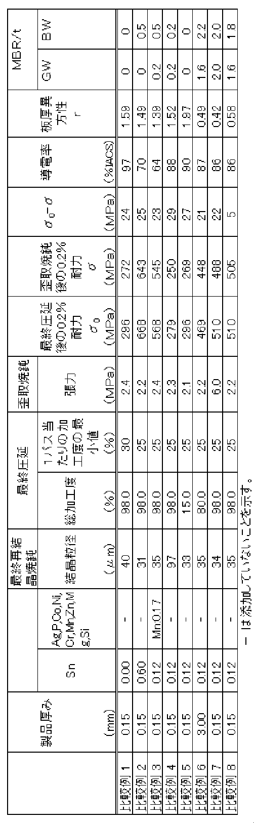
表1に示すところから解かるように、発明例1~32は、いずれも0.01~0.3質量%のSnを含有し、また、最終再結晶焼鈍の結晶粒径が80μm以下、最終圧延の総加工度が20~99%、歪取焼鈍における張力が1~5MPaと規定の範囲になったので、歪取焼鈍後の0.2%耐力が300MPa以上、導電率が75%以上、板厚異方性rが1.0以上で、放熱性、強度および加工性に良好な材料が得られた。さらに、それらの発明例1~32は、最終圧延後の0.2%耐力と歪取焼鈍後における0.2%耐力の差が10~50MPaであるため、曲げ加工性がGW、BW共に1.5以下で良好であった。
一方、表2に示すように、比較例1はSn濃度が0.01質量%未満であり、0.2%耐力が300MPa未満であった。比較例2は、Sn濃度が0.3質量%を超え、導電率が75%未満となって放熱性が悪い。
比較例3は、Sn以外の添加元素濃度が0.15質量%を超え、導電率が75%未満となって放熱性が悪い。
比較例4は、再結晶焼鈍における結晶粒径が80μmを超えたため、0.2%耐力が300MPa未満であった。
比較例5は、最終圧延における総加工度が20%未満であったため、0.2%耐力が300MPa未満であった。
比較例6は、製品厚みが2.0mmを超えたため、板厚異方性が1.0未満となり、絞り加工性が悪い。また、GW、BW共に曲げ加工性が1.5を超えた。
比較例7は、歪取焼鈍を行ったが、張力が5MPaを超えたため、板厚異方性が1.0未満となり、絞り加工性が悪い。また、GW、BW共に曲げ加工性が1.5を超えた。
比較例8は、最終圧延後の0.2%耐力と歪取焼鈍後の0.2%耐力との差が10未満であったため、板厚異方性rが1.0未満となり、絞り加工性が悪い。また、GW、BW共に曲げ加工性が1.5を超えた。
Claims (4)
- 0.01~0.3質量%のSnを含有し、残部が銅およびその不可避的不純物から成り、75%IACS以上の導電率、および300MPa以上の0.2%耐力を有し、かつ、圧延方向に対し、平行な方向、直角な方向および、45°をなす方向のそれぞれのランクフォード値をそれぞれr0、r90、r45としたときに、(r0+r90+2×r45)/4で定義される板厚異方性rが1.0以上である銅合金板。
- W曲げ試験における圧延平行方向(GW方向)および圧延直角方向(BW方向)の最小曲げ半径(MBR)の、板厚(t)に対する割合が、MBR/t≦1.5で与えられる請求項1に記載の銅合金板。
- Ag、P、Co、Ni、Cr、Mn、Zn、Mg、Siからなる群から選ばれる少なくとも1種を合計0.15質量%以下でさらに含有する、請求項1または2に記載の銅合金板。
- 請求項1~3の何れか1項に記載の銅合金板を備える放熱用電子部品。
Priority Applications (2)
| Application Number | Priority Date | Filing Date | Title |
|---|---|---|---|
| CN201480061144.6A CN105705666B (zh) | 2013-11-08 | 2014-06-10 | 铜合金板及具备该铜合金板的散热用电子零件 |
| KR1020167015140A KR101786411B1 (ko) | 2013-11-08 | 2014-06-10 | 구리 합금판 및 그것을 구비하는 방열용 전자 부품 |
Applications Claiming Priority (2)
| Application Number | Priority Date | Filing Date | Title |
|---|---|---|---|
| JP2013-232380 | 2013-11-08 | ||
| JP2013232380A JP5822895B2 (ja) | 2013-11-08 | 2013-11-08 | 銅合金板および、それを備える放熱用電子部品 |
Publications (1)
| Publication Number | Publication Date |
|---|---|
| WO2015068420A1 true WO2015068420A1 (ja) | 2015-05-14 |
Family
ID=53041209
Family Applications (1)
| Application Number | Title | Priority Date | Filing Date |
|---|---|---|---|
| PCT/JP2014/065366 Ceased WO2015068420A1 (ja) | 2013-11-08 | 2014-06-10 | 銅合金板および、それを備える放熱用電子部品 |
Country Status (5)
| Country | Link |
|---|---|
| JP (1) | JP5822895B2 (ja) |
| KR (1) | KR101786411B1 (ja) |
| CN (1) | CN105705666B (ja) |
| TW (1) | TWI545209B (ja) |
| WO (1) | WO2015068420A1 (ja) |
Cited By (1)
| Publication number | Priority date | Publication date | Assignee | Title |
|---|---|---|---|---|
| CN117165811A (zh) * | 2019-03-04 | 2023-12-05 | Jx金属株式会社 | 二次电池负极集电体用轧制铜箔、使用该铜箔的二次电池负极集电体和二次电池、以及二次电池负极集电体用轧制铜箔的制造方法 |
Families Citing this family (4)
| Publication number | Priority date | Publication date | Assignee | Title |
|---|---|---|---|---|
| CN107400799A (zh) * | 2017-08-07 | 2017-11-28 | 苏州列治埃盟新材料技术转移有限公司 | 一种用于机车电子硬件设备的铜基合金材料及其制备方法 |
| JP6783342B2 (ja) * | 2019-04-12 | 2020-11-11 | 日鉄ステンレス株式会社 | オーステナイト系ステンレス鋼およびその製造方法 |
| CN111128944B (zh) * | 2019-12-30 | 2021-12-10 | 南通南平电子科技有限公司 | 一种高性能电容引线框架 |
| JP7816931B2 (ja) * | 2021-06-28 | 2026-02-18 | Dowaメタルテック株式会社 | 銅合金板材および銅合金板材の製造方法 |
Citations (3)
| Publication number | Priority date | Publication date | Assignee | Title |
|---|---|---|---|---|
| JP2009097075A (ja) * | 2007-09-28 | 2009-05-07 | Nikko Kinzoku Kk | 銅合金箔及びそれを用いたフレキシブルプリント基板 |
| WO2012026611A1 (ja) * | 2010-08-27 | 2012-03-01 | 古河電気工業株式会社 | 銅合金板材及びその製造方法 |
| JP5427968B1 (ja) * | 2013-03-29 | 2014-02-26 | Jx日鉱日石金属株式会社 | 銅合金板および、それを備える放熱用電子部品 |
Family Cites Families (8)
| Publication number | Priority date | Publication date | Assignee | Title |
|---|---|---|---|---|
| JP4209145B2 (ja) * | 2002-06-28 | 2009-01-14 | 日鉱金属株式会社 | 曲げ加工性に優れた高強度りん青銅条 |
| JP4255330B2 (ja) | 2003-07-31 | 2009-04-15 | 日鉱金属株式会社 | 疲労特性に優れたCu−Ni−Si系合金部材 |
| JP4157899B2 (ja) | 2006-11-17 | 2008-10-01 | 株式会社神戸製鋼所 | 曲げ加工性に優れた高強度銅合金板 |
| JP5312920B2 (ja) | 2008-11-28 | 2013-10-09 | Jx日鉱日石金属株式会社 | 電子材料用銅合金板又は条 |
| JP5320642B2 (ja) * | 2009-04-17 | 2013-10-23 | 株式会社Shカッパープロダクツ | 銅合金の製造方法及び銅合金 |
| JP5432201B2 (ja) | 2011-03-30 | 2014-03-05 | Jx日鉱日石金属株式会社 | 放熱性及び繰り返し曲げ加工性に優れた銅合金板 |
| JP6188273B2 (ja) | 2011-11-18 | 2017-08-30 | Jx金属株式会社 | 放熱性及び繰り返し曲げ加工性に優れた銅合金板 |
| JP5847787B2 (ja) | 2013-11-26 | 2016-01-27 | Jx日鉱日石金属株式会社 | 導電性及び応力緩和特性に優れる銅合金板 |
-
2013
- 2013-11-08 JP JP2013232380A patent/JP5822895B2/ja active Active
-
2014
- 2014-06-10 KR KR1020167015140A patent/KR101786411B1/ko active Active
- 2014-06-10 WO PCT/JP2014/065366 patent/WO2015068420A1/ja not_active Ceased
- 2014-06-10 CN CN201480061144.6A patent/CN105705666B/zh active Active
- 2014-06-12 TW TW103120313A patent/TWI545209B/zh active
Patent Citations (3)
| Publication number | Priority date | Publication date | Assignee | Title |
|---|---|---|---|---|
| JP2009097075A (ja) * | 2007-09-28 | 2009-05-07 | Nikko Kinzoku Kk | 銅合金箔及びそれを用いたフレキシブルプリント基板 |
| WO2012026611A1 (ja) * | 2010-08-27 | 2012-03-01 | 古河電気工業株式会社 | 銅合金板材及びその製造方法 |
| JP5427968B1 (ja) * | 2013-03-29 | 2014-02-26 | Jx日鉱日石金属株式会社 | 銅合金板および、それを備える放熱用電子部品 |
Cited By (1)
| Publication number | Priority date | Publication date | Assignee | Title |
|---|---|---|---|---|
| CN117165811A (zh) * | 2019-03-04 | 2023-12-05 | Jx金属株式会社 | 二次电池负极集电体用轧制铜箔、使用该铜箔的二次电池负极集电体和二次电池、以及二次电池负极集电体用轧制铜箔的制造方法 |
Also Published As
| Publication number | Publication date |
|---|---|
| KR20160083102A (ko) | 2016-07-11 |
| JP5822895B2 (ja) | 2015-11-25 |
| TWI545209B (zh) | 2016-08-11 |
| KR101786411B1 (ko) | 2017-10-17 |
| CN105705666B (zh) | 2018-01-09 |
| CN105705666A (zh) | 2016-06-22 |
| TW201518519A (zh) | 2015-05-16 |
| JP2015093994A (ja) | 2015-05-18 |
Similar Documents
| Publication | Publication Date | Title |
|---|---|---|
| JP5380621B1 (ja) | 導電性及び応力緩和特性に優れる銅合金板 | |
| JP6270417B2 (ja) | 導電性及び応力緩和特性に優れる銅合金板 | |
| JP2015101773A (ja) | 導電性及び応力緩和特性に優れる銅合金板 | |
| JP5467163B1 (ja) | 銅合金板、それを備える放熱用電子部品および、銅合金板の製造方法 | |
| JP6296728B2 (ja) | 導電性及び曲げたわみ係数に優れる銅合金板 | |
| JP5632063B1 (ja) | 銅合金板、並びに、それを備える大電流用電子部品及び放熱用電子部品 | |
| JP5822895B2 (ja) | 銅合金板および、それを備える放熱用電子部品 | |
| JP6128976B2 (ja) | 銅合金および高電流用コネクタ端子材 | |
| WO2014064961A1 (ja) | 導電性及び応力緩和特性に優れる銅合金板 | |
| CN104232979B (zh) | 导电性及弯曲挠度系数优异的铜合金板 | |
| JP2017002407A (ja) | 導電性及び応力緩和特性に優れる銅合金板 | |
| JP5470499B1 (ja) | 銅合金板、並びに、それを備える大電流用電子部品及び放熱用電子部品 | |
| JP2017066532A (ja) | 導電性及び応力緩和特性に優れる銅合金板 | |
| JP5427968B1 (ja) | 銅合金板および、それを備える放熱用電子部品 | |
| JP6246502B2 (ja) | 導電性及び曲げたわみ係数に優れる銅合金板 | |
| CN105838915B (zh) | 铜合金条、具备该铜合金条的大电流用电子元件以及散热用电子元件 | |
| JP2014208861A (ja) | 導電性及び応力緩和特性に優れる銅合金板 | |
| JP2017089011A (ja) | 導電性及び曲げたわみ係数に優れる銅合金板 | |
| JP2014101580A (ja) | 導電性及び応力緩和特性に優れる銅合金板 |
Legal Events
| Date | Code | Title | Description |
|---|---|---|---|
| 121 | Ep: the epo has been informed by wipo that ep was designated in this application |
Ref document number: 14860748 Country of ref document: EP Kind code of ref document: A1 |
|
| NENP | Non-entry into the national phase |
Ref country code: DE |
|
| ENP | Entry into the national phase |
Ref document number: 20167015140 Country of ref document: KR Kind code of ref document: A |
|
| 122 | Ep: pct application non-entry in european phase |
Ref document number: 14860748 Country of ref document: EP Kind code of ref document: A1 |