WO2015049832A1 - 放射線画像検出器及び放射線画像検出システム - Google Patents
放射線画像検出器及び放射線画像検出システム Download PDFInfo
- Publication number
- WO2015049832A1 WO2015049832A1 PCT/JP2014/004602 JP2014004602W WO2015049832A1 WO 2015049832 A1 WO2015049832 A1 WO 2015049832A1 JP 2014004602 W JP2014004602 W JP 2014004602W WO 2015049832 A1 WO2015049832 A1 WO 2015049832A1
- Authority
- WO
- WIPO (PCT)
- Prior art keywords
- radiation
- light
- detection panel
- image detector
- radiation detection
- Prior art date
- Legal status (The legal status is an assumption and is not a legal conclusion. Google has not performed a legal analysis and makes no representation as to the accuracy of the status listed.)
- Ceased
Links
Images






Classifications
-
- G—PHYSICS
- G01—MEASURING; TESTING
- G01T—MEASUREMENT OF NUCLEAR OR X-RADIATION
- G01T1/00—Measuring X-radiation, gamma radiation, corpuscular radiation, or cosmic radiation
- G01T1/16—Measuring radiation intensity
- G01T1/20—Measuring radiation intensity with scintillation detectors
- G01T1/2006—Measuring radiation intensity with scintillation detectors using a combination of a scintillator and photodetector which measures the means radiation intensity
Definitions
- the present invention relates to a radiation image detector and a radiation image detection system using a radiation detection panel.
- Some radiation detection panels used in radiation image detectors have a photoelectric conversion element and TFT formed in a sensor substrate, and a phosphor for converting radiation into visible light is disposed thereon.
- a radiation detection panel when the radiation transmitted through the subject enters the phosphor, the light emission of the corresponding phosphor is photoelectrically converted to obtain a radiation image as electrical information.
- Such a radiation detection panel has characteristics that it causes characteristic fluctuations due to long-term use and a decrease in S / N ratio due to dark current.
- Patent Document 1 in order to improve such characteristics, an apparatus having a light source unit that irradiates each element of the radiation detection panel is proposed.
- a bias light source such as a number of semiconductor laser diodes, light emitting diodes, or electroluminescent foils is employed as the light source unit.
- the radiation detection panel has a laminated structure of a sensor substrate and a phosphor, and is generally brought into close contact with an adhesive or the like to efficiently transmit light emitted from the phosphor to the sensor substrate.
- the transmittance of the adhesive layer may be reduced by using an adhesive.
- a load may be generated on the sensor substrate due to a difference in thermal expansion coefficient between the sensor substrate and the phosphor.
- Patent Document 2 a method for improving the adhesion between the sensor substrate and the phosphor layer by providing a mechanism for holding the sensor substrate and the phosphor inside the housing and moving up and down and pressing the sensor substrate against the inner wall of the housing. Has proposed.
- Patent Documents 3 and 4 disclose an apparatus that is arranged so that the radiation detection panel side faces the radiation incident surface in order to improve the detection efficiency of visible light in the radiation detection panel and improve the image quality of the obtained radiation image.
- Patent Document 4 there is a method for improving the transmittance of radiation and light by prescribing the material and the content of a substance of a diffusive reflector formed in a sensor substrate and a light source unit, preventing coloring of the substrate. Proposed.
- a configuration in which a laminated structure is simply sandwiched and adhered without using an adhesive as in Patent Document 2 is vulnerable to shock and vibration, and the position of each layer cannot be regulated. Furthermore, the structure such as the pressing mechanism is complicated, and the thickness of the radiation image detector increases.
- Patent Document 3 as a means for holding the laminated structure, a position regulating mechanism that presses the radiation detection panel with a frame is used.
- the holding mechanism is larger than the frame of the radiation detection panel, the size of the radiation image detector is increased.
- the flexible cable arranged on the side surface of the radiation detection panel passes through a hole provided in the frame body, it is difficult to route the flexible cable.
- the present invention has been made in view of the above problems, and in a radiological image detector having a light source unit, while miniaturizing the radiographic image detector, the position of the light source unit is regulated and the light source unit is held. And transmission efficiency of light from the light source unit to the radiation detection panel can be improved.
- a radiation image detector includes a radiation detection panel, a housing that houses the radiation detection panel therein, a buffer material that reduces an impact applied to the radiation detection panel, and irradiates the radiation detection panel with light.
- a light source element that emits light
- a light guide layer that uniformly emits the light from the light emitting element in a plane, and the light from the light emitting element in a plane.
- a diffusion layer for uniformly diffusing, and a reflection layer for reflecting light to the radiation detection panel; and the buffer for the light emitting element, the light guide layer, the diffusion layer, and the reflection layer of the light source unit. It is characterized by preloading with a material and making it adhere.
- the size of the radiographic image detector can be reduced, the position of the light source unit can be regulated, and the light source unit can be held.
- the light emitted from can be efficiently transmitted to the radiation detection panel.
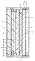
- FIG. 1 is a diagram illustrating the first embodiment, and is a schematic cross-sectional view of a configuration example of a radiation image detector according to the first embodiment.
- the radiation image detector 11 has a housing 12 composed of an upper cover 121 and a frame 122. Inside the housing 12, a radiation detection panel 13, a chassis 14 as an example of a support member, and an electric board 15 are accommodated.
- the radiation detection panel 13 includes a substrate 131, a photoelectric conversion element 132, a phosphor 133, and a reflection plate 134, and has a configuration in which these are stacked.
- the radiation detection panel 13 is assumed to have a quadrilateral shape when viewed from the incident direction of radiation. In FIG. 1, radiation enters from the upper side in the drawing.
- Photoelectric conversion elements 132 are formed in a two-dimensional array on the surface of the substrate 131 by a semiconductor process.
- a phosphor 133 that converts radiation into light is bonded to the surface of the photoelectric conversion element 132.
- An area where the photoelectric conversion element 132 is provided is an effective pixel area X in the radiation incident direction view.
- an area inside the frame B 2 is an effective pixel area X.
- the reflecting plate 134 which consists of metals, such as aluminum which is easy to reflect light.
- the radiation detection panel 13 is fixed to the chassis 14 so that the substrate 131 is located on the radiation incident side (upper side in FIG. 1) and the phosphor 133 is located on the opposite side to the radiation incidence side. It is supported. Thereby, the light detection efficiency in the photoelectric conversion element 132 can be improved, and the sharpness of the obtained image can be improved.
- the chassis 14 is an example of a support member, and supports the radiation detection panel 13 inside the housing 12.
- the chassis 14 is provided with a plurality of projecting leg portions 141 on the surface opposite to the surface that supports the radiation detection panel 13. These leg portions 141 are joined to the inner wall of the frame 122. For this reason, a space (gap) is formed between the chassis 14 and the frame 122 of the housing 12.
- the electric board 15 is disposed in this space.
- the radiation detection panel 13 and the electric board 15 are electrically connected via a flexible printed wiring board (FPC) 16.
- the FPC 16 is connected to at least one of the four sides of the radiation detection panel 13. The other end of the FPC 16 is connected to the electric board 15.
- a housing lid 17 is joined to the radiation incident area of the housing 12.
- the housing lid 17 is made of a highly radiation transmissive member such as CFRP.
- a buffer material 18 and a light source unit 19 are arranged between the inner wall of the housing lid 17 and the substrate 131 of the radiation detection panel 13.
- the cushioning material 18 relieves shock and vibration from the outside of the housing 12.
- the light source unit 19 irradiates the radiation detection panel 13 with refreshing light that improves afterimage characteristics. That is, the light source unit 19 removes the charges accumulated in the radiation detection panel 13 by irradiating the radiation detection panel 13 with light.
- the LED backlight as the light source unit 19 includes four diffusion plates 191 and 192 that are examples of the diffusion layer, a light guide plate 193 that is an example of the light guide layer, and a reflection plate 194 that is an example of the reflection layer. It has the structure which has the plate-shaped optical member of a layer, and these laminate. A plurality of light emitting elements 195 that emit refreshing light are arranged on the side surface of the light guide plate 193.
- the light guide plate 193 which is an example of the light guide layer transmits the light emitted from the light emitting element 195 so as to be uniform in the plane (plane direction).
- the diffusion plates 191 and 192 which are examples of the diffusion layer diffuse the light emitted from the light emitting element 195 so as to be uniform in the plane (plane direction).
- the light guide plate 193, the diffusion plate 192, and the light emitting element 195 are sandwiched and fixed by the diffusion plate 191 and the reflection plate 194.
- a spacer 196 is disposed so as to surround the light guide plate 193, the diffusion plate 192, and the light emitting element 195 when viewed in the incident direction of radiation.
- the spacer 196 regulates the height dimension of the light source unit 19 (dimension in the radiation incident direction, the vertical dimension in FIG. 1).
- An adhesive 197 is applied to both ends of the spacer 196 in the height direction (radiation incidence direction).
- the diffusion plate 191 and the reflection plate 194 are joined via a spacer 196 disposed at the peripheral edge thereof. Therefore, as shown in FIG. 1, a closed space is formed by the diffusion plate 191, the spacer 196, and the reflection plate 194.
- a plurality of light emitting elements 195, a diffusion plate 192, and a light guide plate 193 are accommodated in the closed space.
- the plurality of light emitting elements 195, the diffusion plate 192, and the light guide plate 193 are accommodated in the closed space, thereby restricting movement in the plane direction (direction orthogonal to the incident direction of radiation). Is done.
- the light emitting element 195 and the electric board 15 are connected by a cable.
- a circuit for controlling the light source unit 19 and the like are constructed on the electric board 15.
- the light emitting element 195 is turned on in response to an electric signal from the electric board 15.
- the width B 1 of the spacer 196 is made smaller than the width B 2 of the frame of the radiation detection panel 13.
- the spacer 196 is inside the outer edge of the frame of the radiation detection panel 13 when viewed in the incident direction of radiation (as viewed from the upper side in FIG. 1), and the effective pixel region X of the radiation detection panel 13. It is arranged outside.
- the effective pixel region X is as described above. According to such a configuration, the length of the FPC 16 can be shortened, and the radiation image detector 11 can be downsized.
- a plurality of light emitting elements 195 may be two-dimensionally arranged in a plane so as to face the radiation detection panel 13 to form a surface light source.
- a configuration in which a plurality of light emitting elements 195 are provided in place of the light guide plate 193 that is an example of the light guide layer can be applied to the light source unit 19.
- the plurality of light emitting elements 195 may be arranged on the side surface of the diffusion plate 192, or may be arranged in a plane instead of the diffusion plate 192.
- the light source unit 19 and the radiation detection panel 13 are preloaded by pressing the entire surface with the buffer material 18. For this reason, the adhesiveness of the light source part 19 and the radiation detection panel 13 increases, and while restricting the position of a light source member, a light source member can be hold
- the light source unit 19 may be configured to be fixed to the radiation detection panel 13 with an adhesive. Further, an adhesive may be applied to both sides of the buffer material 18 and fixed to the housing lid 17 side. With such a configuration, the adhesive is eliminated between the light source unit 19 and the radiation detection panel 13, so that the light transmittance is further improved.
- the radiation image detector according to the present embodiment by arranging the buffer material 18 in the housing 12, the position of the light source unit 19 can be regulated and the light source unit 19 can be held, and the light source unit The 19 optical members and the radiation detection panel 13 can be brought into close contact with each other. Therefore, in the radiation image detector according to the present embodiment, the light emitted from the light emitting element 195 can be efficiently transmitted to the radiation detection panel 13. Furthermore, in the radiation image detector according to the present embodiment, the spacer 196 is disposed on the periphery of the light emitting element 195 to form a sealed closed space, thereby restricting the position of the optical member configured in the light source unit 19 and optically. The member can be held.
- the second to tenth embodiments can apply the same configuration as the first embodiment except for the light source unit. For this reason, description is abbreviate
- symbol as 1st embodiment may be attached
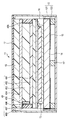
- FIG. 2A and 2B are schematic views showing a cross-sectional structure of the radiation image detector 11 according to the second embodiment.
- FIG. 2B is a sectional view taken along line 2B-2B in FIG. 2A.
- the spacers 296 are arranged at the peripheral portions of the diffusion plate 291 and the reflection plate 294 that are formed in a quadrilateral shape when viewed in the radiation incident direction.
- the diffusing plate 291 of the light source unit 29 and the peripheral portion of the reflecting plate 294 are bonded to the spacer 296 with an adhesive 297.
- the spacer 296 is disposed such that a gap is formed on at least one of the four sides (two sides in FIG. 2B).
- the light guide plate 293 is provided with a hook portion 298 that protrudes outward in the surface direction in accordance with the gap, and the hook portion 298 is fitted into the gap.
- the hanging portion 298 is an example of movement restriction means.
- the light guide plate 293 is provided with the hook portion 298 as an example of the movement restricting unit, and when the hook portion 298 is fitted into the gap of the spacer 296, the movement of the light guide plate 293 in the surface direction is restricted.
- a closed space is formed in the light source unit 29 by the spacer 296, the diffusion plate 291, and the reflection plate 294.
- a hooking portion as a movement restricting unit is formed on the diffusion plate 292 as in the light guide plate 293.
- the movement of the optical member such as the diffusion plate 292 in the surface direction can be restricted. Therefore, when the posture of the housing 12 changes or when shock or vibration is applied to the housing 12, the movement in the in-plane direction (direction orthogonal to the radiation incident direction) of each layer (plate-like optical member) The load on the light emitting element 295 can be reduced. Further, the light emitting element 295 and the light guide plate 293 can be positioned, and the light transmission efficiency can be improved.
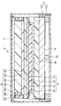
- FIG. 3 is a diagram for explaining the third embodiment, and is a schematic cross-sectional view of the radiation image detector 11.
- the peripheral portions of the diffusion plate 391 and the reflection plate 394 and the spacer 396 are applied to the top and bottom of the spacer 396. Glued by 397.
- a closed space is formed by the spacer 396, the diffusion plate 391, and the reflection plate 394.
- a diffuser plate 392, a light guide plate 393, and a light emitting element 395 are accommodated in the closed space.
- an adhesive 397 is applied to the inner peripheral side of the spacer 396.
- the side surface of the diffusion plate 392 and the side surface of the light guide plate 393 are bonded to the inner peripheral surface of the spacer 396 by an adhesive 397.
- FIG. 4 is a diagram for explaining the fourth embodiment, and is a schematic cross-sectional view of the radiation image detector 11.
- the peripheral portions of the diffusion plate 491 and the reflection plate 494 and the spacer 496 are applied to the top and bottom of the spacer 496. Glued by 497.
- a closed space is formed by the diffusion plate 491, the reflection plate 494, and the spacer 496.
- a diffusion plate 492, a light guide plate 493, and a light emitting element 495 are accommodated.
- a reflection plate 498 which is an example of a reflection material, is disposed on the inner peripheral side of the spacer 496 (the light guide plate 493 side).
- the reflection plate 498 which is an example of a reflection material and transmitted to the radiation detection panel 13. Therefore, the light emitted from the light emitting element 495 can be efficiently transmitted to the radiation detection panel 13.
- the reflector 498 instead of using the reflector 498 as the reflector, a configuration in which a material that reflects light is provided in the spacer 496 (a configuration in which the reflector is provided in the spacer 496) may be used.
- the spacer 496 may be configured such that the inner periphery side of the spacer 496 is coated with a material that reflects light (a coating of a reflective material).
- FIG. 5 is a diagram for explaining the fifth embodiment, and is a schematic cross-sectional view of the radiation image detector 11.
- the peripheral edge portion of the substrate 131 of the radiation detection panel 13 and the peripheral edge portion of the reflection plate 594 of the light source unit 59 are joined via a spacer 596.
- an adhesive 597 is applied to the top and bottom of the spacer 596, and the peripheral edge of the substrate 131 and the peripheral edge of the reflector 594 are bonded to the spacer 596 by the adhesive 597.
- a closed space is formed by the substrate 131, the reflection plate 594, and the spacer 596.
- Two diffusion plates 591, 592, a light guide plate 593, and a light emitting element 595 are accommodated in the closed space.
- the radiation detection panel 13 may be easily damaged.
- the radiation detection panel 13 and the light source unit 59 are joined to reinforce the radiation detection panel 13.
- the frame of the radiation detection panel 13 is bonded to the spacer 596, and the adhesive 597 is not applied to the radiation effective region. Thereby, the light transmittance is improved.
- FIG. 6 is a diagram for explaining the sixth embodiment, and is a schematic cross-sectional view of the radiation image detector 11.
- the peripheral portions of the diffusion plate 691 and the reflection plate 684 are bonded to the spacer 696 with an adhesive 697 applied to the top and bottom of the spacer 696.
- a closed space is formed by the spacer 696, the diffusion plate 691, and the reflection plate 694.
- a diffusion plate 692, a light guide plate 693, and a light emitting element 695 are accommodated in the closed space.
- a buffer material 68 is disposed between the radiation detection panel 13 and the chassis 14.
- the cushioning material 68 reduces the impact and vibration from the outside of the housing 12.
- the radiation detection panel 13 is joined to the buffer material 68.
- the light source unit 69 and the radiation detection panel 13 are preloaded by pressing the entire surface with the buffer material 68. For this reason, the adhesiveness of the light source part 69 and the radiation detection panel 13 increases. Therefore, the light emitted from the light emitting element 695 is efficiently transmitted to the radiation detection panel 13. With such a configuration, an image with improved afterimage characteristics can be obtained.
- the light source unit 69 is bonded and fixed to the housing lid 17. With such a configuration, there is no adhesive between the light source unit 69 and the radiation detection panel 13, so that the light transmittance can be further improved.
- FIG. 7 is a diagram for explaining the seventh embodiment and is a schematic cross-sectional view of the radiation image detector 11.
- the peripheral edge portions of the diffusion plate 791 and the reflection plate 794 are bonded to the spacer 796 by an adhesive 797 applied to the top and bottom of the spacer 796.
- a closed space surrounded by the diffusion plate 791, the reflection plate 794, and the spacer 796 is formed.
- a diffusion plate 792, a light guide plate 793, and a light emitting element 795 are accommodated.
- the light source unit 79 is fixed to the chassis 14 as shown in FIG.
- the radiation detection panel 13 is arranged so that the substrate 131 is in contact with the radiation incident surface (here, the diffusion plate 791) of the light source unit 79.
- a buffer material 78 is disposed between the inner wall of the housing lid 17 and the reflection plate 134 of the radiation detection panel 13.
- the cushioning material 78 reduces the impact and vibration from the outside of the housing 12.
- the light source unit 79 and the radiation detection panel 13 are pre-pressed with the entire surface pressed by the buffer material 78. For this reason, the adhesiveness of the light source part 79 and the radiation detection panel 13 increases. Accordingly, the light emitted from the light emitting element 795 is efficiently transmitted to the radiation detection panel 13, so that an image with improved afterimage characteristics can be obtained.
- FIG. 8 is a diagram for explaining the eighth embodiment, and is a schematic cross-sectional view of the radiation image detector 11.
- the peripheral portions of the diffusion plate 891 and the reflection plate 894 are bonded to the spacer 896 by an adhesive 897 applied to the top and bottom of the spacer 896.
- a closed space is formed so as to be surrounded by the diffusion plate 891, the reflection plate 894, and the spacer 896.
- a diffusion plate 892, a light guide plate 893, and a light emitting element 895 are accommodated.
- the buffer material 88 is disposed between the light source unit 89 and the chassis 14.
- the cushioning material 88 reduces the impact and vibration from the outside of the housing 12.
- the light source unit 89 is bonded to the buffer material 88.
- the light source unit 89 and the radiation detection panel 13 are pre-pressed by being pressed down by the buffer material 88. For this reason, the adhesiveness of the light source part 89 and the radiation detection panel 13 increases. Accordingly, the light emitted from the light emitting element 895 is efficiently transmitted to the radiation detection panel 13, so that an image with improved afterimage characteristics can be obtained.
- the radiation detection panel 13 is fixed by being joined to the housing lid 17. With such a configuration, the light transmittance is further improved because there is no adhesive between the light source unit 89 and the radiation detection panel 13.
- FIG. 9 is a diagram for explaining the ninth embodiment, and is a schematic cross-sectional view of the radiation image detector 11.
- the peripheral edge of the diffusing plate 991 and the housing lid 17 are bonded to the spacer 996 by an adhesive 997 applied to the top and bottom of the spacer 996.
- a closed space surrounded by the diffusion plate 991, the housing lid 17, and the spacer 996 is formed.
- a diffusion plate 992, a light guide plate 993, a reflection plate 994, and a light emitting element 995 are accommodated.
- the buffer material 98 is disposed between the radiation detection panel 13 and the chassis 14.
- the cushioning material 98 relieves shock and vibration from the outside of the housing 12.
- the radiation detection panel 13 is joined to the buffer material 98.
- the spacer 996 is made of a material having high thermal conductivity such as silicon carbide.
- the spacer 996 for example, heat radiating rubber using silicone as a base material can be used.
- the spacer 996 is formed of a material that can dissipate heat generated from the light emitting element 955, the spacer 996 is closely attached to the light emitting element 995, and the heat generated by the light emitting element 995 is easily radiated through the spacer 996. . Thereby, formation of a hot spot can be suppressed.
- the spacer 996 is joined to the housing lid 17. With such a structure, heat of the light emitting element 995 can be released to the housing 12.
- FIG. 10 is a diagram for explaining the tenth embodiment and is a schematic cross-sectional view of the radiation image detector 11.
- the peripheral portions of the diffusion plate 1091 and the chassis 14 are bonded to the spacer 1096 by an adhesive 1097 applied to the top and bottom of the spacer 1096.
- a closed space surrounded by the diffusion plate 1091, the chassis 14, and the spacer 1096 is formed.
- a diffusion plate 1092, a light guide plate 1093, a reflection plate 1094, and a light emitting element 1095 are accommodated.
- the buffer material 108 is provided between the housing lid 17 and the radiation detection panel 13.
- the radiation detection panel 13 and the light source unit 109 are preloaded by the buffer material 108. Therefore, the same effects as those of the first to ninth embodiments are obtained.
- a material having high thermal conductivity is applied to the spacer 1096 as in the ninth embodiment, and the light emitting element 195 is in close contact with the spacer 1096. Furthermore, as shown in FIG. 10, the spacer 1096 is bonded to the chassis 14, so that the heat of the light emitting element 1095 can be released. Accordingly, formation of hot spots due to the light-emitting element 1095 can be suppressed.
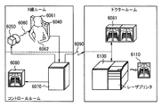
- FIG. 11 is a diagram showing an application example of any of the above-described radiation image detectors to an X-ray diagnostic system (radiation image detection system).
- X-ray 6060 as radiation generated in the X-ray tube 6050 (radiation source) passes through the chest 6062 of the subject or patient 6061 and enters the detector 6040 which is one of the above-described radiographic image detectors.
- This incident X-ray includes information inside the body of the patient 6061.
- the phosphor emits light in response to the incidence of X-rays, and this light is photoelectrically converted to obtain electrical information.
- the radiological image detection system includes at least a radiographic image detector and a signal processing unit that processes a signal from the radiographic image detector.
- this information can be transferred to a remote place by a transmission processing unit such as a telephone line 6090 and can be displayed on a display 6081 serving as a display unit such as a doctor room in another place or stored in a recording unit such as an optical disk.
- a remote doctor can make a diagnosis based on the information.
- it can also record on the film 6110 used as a recording medium by the film processor 6100 used as a recording part.
Landscapes
- Physics & Mathematics (AREA)
- Health & Medical Sciences (AREA)
- Life Sciences & Earth Sciences (AREA)
- General Physics & Mathematics (AREA)
- High Energy & Nuclear Physics (AREA)
- Molecular Biology (AREA)
- Spectroscopy & Molecular Physics (AREA)
- Measurement Of Radiation (AREA)
Abstract
放射線画像検出器は、放射線検出パネルと、内部に放射線検出パネルを収納する筐体と、放射線検出パネルの衝撃を緩和する緩衝材と、放射線検出パネルに光を照射する光源部とを有する。光源部は、発光素子と、発光素子からの光を平面内に均一に発光させる導光層と、発光素子からの光を均一に拡散させる拡散層と、放射線検出パネルへ光を反射させる反射層とを有する。光源部の発光素子と導光層と拡散層と反射層とは、緩衝材で予圧されて密着している。
Description
本発明は、放射線検出パネルを用いた放射線画像検出器及び放射線画像検出システムに関する。
放射線画像検出器に使用される放射線検出パネルには、光電変換素子とTFTがセンサ基板内に形成され、この上に放射線を可視光に変換するための蛍光体が配置されたものがある。このような放射線検出パネルは、被検者を透過した放射線が蛍光体に入射すると、これに対応した蛍光体の発光を光電変換して放射線像を電気的情報として得ている。
このような放射線検出パネルは、長時間の使用による特性変動や、ダーク電流によるS/N比の低下を招くという特性を有する。特許文献1では、このような特性を改善するため、放射線検出パネルの各素子に光を照射する光源部を有する装置が提案されている。特許文献1においては、多数の半導体レーザーダイオード、発光ダイオード、又はエレクトロルミネセント箔のようなバイアス光源を光源部として採用している。
一方、放射線検出パネルは、センサ基板と蛍光体の積層構造を有しており、一般的に接着剤等で密着させて、蛍光体から発光した光を効率よくセンサ基板に伝達させる。しかし、接着剤を用いることによって、接着層の透過率が低下することがある。また、センサ基板と蛍光体の熱膨張係数の違いにより、センサ基板へ負荷が生じることがある。特許文献2では、筐体内部にセンサ基板と蛍光体を保持し、昇降するような機構を設け、筐体内壁にセンサ基板を押しつけることによって、センサ基板と蛍光体層の密着性を向上させる手法を提案している。
特許文献3や特許文献4には、放射線検出パネルにおける可視光の検出効率を高め、得られる放射線画像の画質を向上させるために、放射線検出パネル側が放射線入射側の面を向くように配置する装置が提案されている。特に、特許文献4では、センサ基板や光源部に構成される拡散反射板の材質や物質の含有量について規定し、基板への着色を防止させて、放射線や光の透過率を向上させる手法が提案されている。
特許文献1に記載の構成では、反射板と、導光板と、拡散板との各層の間に接着剤が充填されて貼り合わせられる。この構成では、接着剤の層により光の透過率が減衰してしまう。さらに、各光学部材が接着された構成では、膨張係数が異なると、急激な温度変化が生じた場合に光源部が破損するおそれがある。
特許文献2のような、接着剤を用いずに積層構造を単純に挟み込んで密着させた構成では、衝撃や振動に弱く、各層の位置が規制できない。さらには、押付機構など構造が複雑となる上、放射線画像検出器の厚さも増してしまう。
特許文献3では、積層構造を保持する手段として、放射線検出パネルを枠体で押さえつけるような位置規制機構を用いている。しかし、保持機構が放射線検出パネルの額縁よりも大きくなるため、放射線画像検出器のサイズが大きくなってしまう。さらには、放射線検出パネルの側面に配置されたフレキシブルケーブルは枠体に設けた穴を通すために、引き回しが困難となる。
本発明は、上記課題を鑑みてなされたものであり、光源部を有する放射線画像検出器において、放射線画像検出器の小型化を実現しつつ、光源部の位置を規制するとともに光源部を保持することができ、光源部から放射線検出パネルへの光の伝達効率を向上させることができる。
本発明に係る放射線画像検出器は、放射線検出パネルと、内部に前記放射線検出パネルを収納する筐体と、前記放射線検出パネルにかかる衝撃を緩和する緩衝材と、前記放射線検出パネルに光を照射する光源部と、を有し、前記光源部は、光を発する発光素子と、前記発光素子からの光を平面内に均一に発光させる導光層と、前記発光素子からの光を平面内に均一に拡散させる拡散層と、前記放射線検出パネルへ光を反射させる反射層と、を有し、前記光源部の前記発光素子と前記導光層と前記拡散層と前記反射層とを、前記緩衝材で予圧して密着させることを特徴とする。
本発明にかかわる放射線画像検出器によれば、緩衝材を設けることによって、放射線画像検出器の小型化を実現しつつ、光源部の位置を規制するとともに光源部を保持することができ、発光素子から発光した光を効率よく放射線検出パネルに伝達することができる。
(第一の実施形態)
図1は、第一の実施形態を説明する図であり、第一の実施形態における放射線画像検出器の構成例の断面模式図である。
図1は、第一の実施形態を説明する図であり、第一の実施形態における放射線画像検出器の構成例の断面模式図である。
放射線画像検出器11は、上カバー121とフレーム122とで構成される筐体12を有する。筐体12の内部には、放射線検出パネル13と、支持部材の例であるシャシー14と、電気基板15とが収納される。
放射線検出パネル13は、基板131と、光電変換素子132と、蛍光体133と、反射板134とを含み、これらが積層された構成を有する。また、放射線検出パネル13は、放射線の入射方向から見て、四辺形の形状をなすものとする。図1においては、図中の上側から放射線が入射する。
放射線検出パネル13の基板131には、たとえばガラス板が用いられる。これは、半導体素子との化学作用のないことと、半導体プロセスの温度に耐えることと、寸法安定性等の必要性とによる。基板131の表面には、光電変換素子132が半導体プロセスにより二次元配列的に形成される。光電変換素子132の表面には、放射線を光に変換する蛍光体133が接合される。放射線の入射方向視において、光電変換素子132が設けられる領域が、有効画素領域Xとなる。図1に示すように、額縁B2よりも内側の領域が、有効画素領域Xとなる。そして、これらは、光を反射しやすいアルミ等の金属からなる反射板134で覆われている。
放射線検出パネル13は、放射線の入射される側(図1では上側)に基板131が位置し、放射線の入射される側とは反対側に蛍光体133が位置するように、シャシー14に固定されて支持されている。これにより、光電変換素子132における光の検出効率を向上させることができ、得られた画像の鮮鋭度を向上させることができる。
シャシー14は支持部材の例であり、筐体12の内部において、放射線検出パネル13を支持する。シャシー14には、放射線検出パネル13を支持する面とは反対側の面に、複数の突出する脚部141が設けられる。そして、これら脚部141は、フレーム122の内壁に接合されている。このため、シャシー14と筐体12のフレーム122との間には、空間(隙間)が形成される。この空間には、電気基板15が配置される。そして、放射線検出パネル13と電気基板15とは、フレキシブルプリント配線板(FPC)16を介して電気的に接続されている。本実施形態では、放射線検出パネル13の4辺のうち、少なくとも1辺に、FPC16が接続されている。FPC16の他端は、電気基板15に接続されている。
筐体12における放射線入射領域には、筐体蓋17が接合されている。筐体蓋17は、CFRP等の放射線透過性の高い部材からなる。筐体蓋17の内壁と放射線検出パネル13の基板131との間には、緩衝材18と光源部19とが配置される。緩衝材18は、筐体12の外部からの衝撃や振動を緩和する。光源部19は、放射線検出パネル13に、残像特性を改善するリフレッシュ光を照射する。すなわち、光源部19は、放射線検出パネル13に光を照射することにより、放射線検出パネル13に貯まった電荷を除去する。
光源部19としては、LEDバックライトを用いることができる。LEDバックライトは、高出力、小型、低価格化が進み、液晶テレビ等でも多く使用されている。光源部19としてのLEDバックライトは、拡散層の例である2枚の拡散板191,192と、導光層の例である導光板193と、反射層の例である反射板194との4層の板状の光学部材を有し、これらが積層する構成を有する。導光板193の側面には、リフレッシュ光を発する複数の発光素子195が配列されている。導光層の例である導光板193は、発光素子195が発する光を、平面内(面方向)に均一なるように伝達する。拡散層の例である拡散板191,192は、発光素子195が発する光を、平面内(面方向)に均一になるように拡散する。導光板193と、拡散板192と、発光素子195とは、拡散板191と反射板194によって挟まれて固定される。放射線の入射方向視において、導光板193と、拡散板192と、発光素子195とを囲むように、スペーサ196が配置される。スペーサ196は、光源部19の高さ寸法(放射線の入射方向の寸法、図1中では上下方向寸法)を規制する。スペーサ196の高さ方向(放射線の入射方向)の両端には接着剤197が塗布されている。
そして、拡散板191と反射板194は、それらの周縁部に配置されるスペーサ196を介して接合される。このため、図1に示すように、拡散板191とスペーサ196と反射板194とにより閉空間が形成される。この閉空間の内部には、複数の発光素子195と、拡散板192と、導光板193とが収納される。このように、複数の発光素子195と、拡散板192と、導光板193とは、この閉空間の内部に収納されることによって、面方向(放射線の入射方向に直交する方向)の移動が規制される。
また、発光素子195と電気基板15はケーブルで接続されている。電気基板15には、光源部19を制御する回路などが構築されている。発光素子195は、電気基板15からの電気信号に応じて点灯する。
ここで、図1に示すように、スペーサ196の幅B1は、放射線検出パネル13の額縁の幅B2よりも小さくされる。そして、スペーサ196は、放射線の入射方向視において(図1においては図中の上側から見て)、放射線検出パネル13の額縁の外縁の内側であって、かつ放射線検出パネル13の有効画素領域Xよりも外側に配置される。なお、有効画素領域Xは前記のとおりである。このような構成によれば、FPC16の引き回しの長さを短くすることができ、放射線画像検出器11を小型化することができる。
なお、複数の発光素子195が、放射線検出パネル13に対向するように、平面内に二次元状に配置されて面光源を形成する構成であってもよい。この場合には、光源部19には、複数の発光素子195が導光層の例である導光板193に代えて設けられる構成が適用できる。このように、複数の発光素子195が拡散板192の側面に配置される構成であってもよく、拡散板192に代えて平面内に配置される構成であってもよい。
光源部19および放射線検出パネル13は、緩衝材18で全面を押さえつけられて予圧される。このため、光源部19および放射線検出パネル13の密着性が増し、光源部材の位置を規制するとともに光源部材を保持することができる。したがって、発光素子195が発した光は、効率よく放射線検出パネル13に照射され、放射線検出パネル13に貯まった電荷を除去する。これにより、残像特性を改善した画像を得ることができる。なお、光源部19は、放射線検出パネル13に接着剤によって固定される構成であってもよい。また、緩衝材18の両側に接着剤が塗布され、筐体蓋17の側に固定される構成であってもよい。このような構成であると、光源部19と放射線検出パネル13の間に接着剤がなくなるため、光の透過率が一層向上する。
したがって、本実施例による放射線画像検出器によれば、筐体12に緩衝材18を配置することによって、光源部19の位置を規制するとともに光源部19を保持することができ、且つ、光源部19の光学部材と放射線検出パネル13を密着させることができる。そのため、本実施例による放射線画像検出器では、発光素子195から発光した光を効率よく放射線検出パネル13に伝達することができる。さらに、本実施例による放射線画像検出器では、発光素子195の周縁にスペーサ196を配置し、密閉された閉空間を形成することで光源部19に構成される光学部材の位置を規制するとともに光学部材を保持することができる。
次に、第二~第十の実施形態について説明する。なお、第二~第十の実施形態は、光源部を除いて第一の実施形態と共通の構成が適用できる。このため、第一の実施形態と共通の構成については説明を省略する。なお、第一の実施形態と共通の構成には、第一の実施形態と同じ符号を付して示すことがある。
(第二の実施形態)
図2A及び図2Bは、第二の実施形態にかかる放射線画像検出器11の断面構造を示す模式図である。図2Bは図2Aの2B‐2B線に沿った断面図である。第二の実施形態では、放射線の入射方向視において、スペーサ296が、四辺形に形成される拡散板291と反射板294の周縁部に配置される。そして、第一の実施形態と同様に、光源部29の拡散板291と反射板294の周縁部が、接着剤297によって、スペーサ296に接着されている。ただし、スペーサ296は、四辺のうちの少なくとも1辺(図2Bでは2辺)に隙間が生じるように配置される。そして導光板293には、隙間に合わせて面方向外側に突出する掛かり部298を設けられ、掛かり部298が隙間に嵌まりこむ。掛かり部298は移動規制手段の例である。このように、導光板293に移動規制手段の例として掛かり部298が設けられ、この掛かり部298がスペーサ296の隙間に嵌まり込むことによって、導光板293の面方向の移動が規制される。
図2A及び図2Bは、第二の実施形態にかかる放射線画像検出器11の断面構造を示す模式図である。図2Bは図2Aの2B‐2B線に沿った断面図である。第二の実施形態では、放射線の入射方向視において、スペーサ296が、四辺形に形成される拡散板291と反射板294の周縁部に配置される。そして、第一の実施形態と同様に、光源部29の拡散板291と反射板294の周縁部が、接着剤297によって、スペーサ296に接着されている。ただし、スペーサ296は、四辺のうちの少なくとも1辺(図2Bでは2辺)に隙間が生じるように配置される。そして導光板293には、隙間に合わせて面方向外側に突出する掛かり部298を設けられ、掛かり部298が隙間に嵌まりこむ。掛かり部298は移動規制手段の例である。このように、導光板293に移動規制手段の例として掛かり部298が設けられ、この掛かり部298がスペーサ296の隙間に嵌まり込むことによって、導光板293の面方向の移動が規制される。
図2Aに示すように、光源部29には、スペーサ296と拡散板291と反射板294とにより閉空間が形成される。この閉空間に拡散板292などの光学部材が収納される構成である場合には、図2Bに示すように、導光板293と同様に、拡散板292に移動規制手段としての掛かり部が形成される構成が適用できる。このような構成によれば、これらの拡散板292などの光学部材の面方向の移動を規制することができる。したがって、筐体12の姿勢が変わった場合や、筐体12に衝撃・振動が加わった場合に、各層(板状の光学部材)の面内方向(放射線の入射方向に直交する方向)の移動を規制し、発光素子295への負荷軽減を図ることができる。さらに、発光素子295と導光板293との位置決めができ、光の伝達効率を向上することができる。
(第三の実施形態)
図3は第三の実施形態を説明する図であり、放射線画像検出器11の断面模式図である。第三の実施形態では、第一の実施形態と同様に、光源部39において、拡散板391と反射板394のそれぞれの周縁部と、スペーサ396とが、スペーサ396の上下に塗布された接着剤397によって接着される。そして、スペーサ396と、拡散板391と、反射板394とにより閉空間が形成される。この閉空間の内部には、拡散板392と、導光板393と、発光素子395とが収納される。
図3は第三の実施形態を説明する図であり、放射線画像検出器11の断面模式図である。第三の実施形態では、第一の実施形態と同様に、光源部39において、拡散板391と反射板394のそれぞれの周縁部と、スペーサ396とが、スペーサ396の上下に塗布された接着剤397によって接着される。そして、スペーサ396と、拡散板391と、反射板394とにより閉空間が形成される。この閉空間の内部には、拡散板392と、導光板393と、発光素子395とが収納される。
さらに、図3に示すように、スペーサ396の内周側に接着剤397が塗布される。そして、拡散板392の側面と導光板393の側面は、接着剤397によってスペーサ396の内周面に接着される。このような構成によれば、筐体12の姿勢が変わった場合や、筐体12に衝撃・振動が加わった場合に、各層(板状の光学部材)の面内方向(放射線の入射方向に直交する方向)の移動を規制できる。したがって、発光素子395への負荷軽減を図ることができる。また、発光素子395と導光板393との位置決めができ、光の伝達効率を向上することができる。さらに、第二の実施形態と組み合わせて実施することによって、効果は一層向上する。
(第四の実施形態)
図4は、第四の実施形態を説明する図であり、放射線画像検出器11の断面模式図である。第四の実施形態では、第一の実施形態と同様に、光源部49において、拡散板491と反射板494のそれぞれの周縁部と、スペーサ496とが、スペーサ496の上下に塗布された接着剤497によって接着される。これにより、拡散板491と、反射板494と、スペーサ496とによって、閉空間が形成される。そして、この閉空間の内部には、拡散板492と、導光板493と、発光素子495とが収納される。
図4は、第四の実施形態を説明する図であり、放射線画像検出器11の断面模式図である。第四の実施形態では、第一の実施形態と同様に、光源部49において、拡散板491と反射板494のそれぞれの周縁部と、スペーサ496とが、スペーサ496の上下に塗布された接着剤497によって接着される。これにより、拡散板491と、反射板494と、スペーサ496とによって、閉空間が形成される。そして、この閉空間の内部には、拡散板492と、導光板493と、発光素子495とが収納される。
さらに、図4に示すように、スペーサ496の内周側(導光板493の側)には、反射材の例である反射板498が配置される。このような構成であると、導光板493や拡散板492の側面から漏れた光は、反射材の例である反射板498で反射し、放射線検出パネル13に伝達する。したがって、発光素子495から発光した光を、放射線検出パネル13に効率よく伝達させることができる。なお、反射材として反射板498を用いる代わりに、スペーサ496に光を反射する素材が設けられる構成(反射材がスペーサ496に設けられる構成)であってもよい。また、スペーサ496の内周側に、光を反射する材料のコーティング(反射材のコーティング)が施される構成であってもよい。
(第五の実施形態)
図5は、第五の実施形態を説明する図であり、放射線画像検出器11の断面模式図である。図5に示すように、放射線検出パネル13の基板131の周縁部と、光源部59の反射板594の周縁部とが、スペーサ596を介して接合される。たとえば、スペーサ596の上下に接着剤597が塗布され、この接着剤597によって、基板131の周縁部と反射板594の周縁部のそれぞれとが、スペーサ596に接着される。そして、基板131と、反射板594と、スペーサ596とで、閉空間が形成される。この閉空間の内部に、2つの拡散板591,592と、導光板593と、発光素子595とが収納される。
図5は、第五の実施形態を説明する図であり、放射線画像検出器11の断面模式図である。図5に示すように、放射線検出パネル13の基板131の周縁部と、光源部59の反射板594の周縁部とが、スペーサ596を介して接合される。たとえば、スペーサ596の上下に接着剤597が塗布され、この接着剤597によって、基板131の周縁部と反射板594の周縁部のそれぞれとが、スペーサ596に接着される。そして、基板131と、反射板594と、スペーサ596とで、閉空間が形成される。この閉空間の内部に、2つの拡散板591,592と、導光板593と、発光素子595とが収納される。
なお、基板131を透過した放射線が蛍光体133に入射し、これにより蛍光体133が発光するような構成の場合には、放射線の透過率を向上させるため、基板131には薄型のガラス基板を用いることができる。そのため、図5に示すように、蛍光体133が基板131より小さく、基板131とシャシー14との間に隙間が生じていると、放射線検出パネル13が破損しやすくなるおそれがある。そこで、第五の実施形態では、放射線検出パネル13と光源部59とが接合されることによって、放射線検出パネル13が補強される。ここで、放射線検出パネル13の額縁のみがスペーサ596と接着され、放射線有効領域には接着剤597が塗布されない。これにより、光の透過率が向上する。
(第六の実施形態)
図6は、第六の実施形態を説明する図であり、放射線画像検出器11の断面模式図である。拡散板691と反射板684のそれぞれの周縁部が、スペーサ696の上下に塗布された接着剤697によってこのスペーサ696に接着される。そして、スペーサ696と拡散板691と反射板694とによって閉空間が形成される。この閉空間の内部に、拡散板692と、導光板693と、発光素子695とが収納される。
図6は、第六の実施形態を説明する図であり、放射線画像検出器11の断面模式図である。拡散板691と反射板684のそれぞれの周縁部が、スペーサ696の上下に塗布された接着剤697によってこのスペーサ696に接着される。そして、スペーサ696と拡散板691と反射板694とによって閉空間が形成される。この閉空間の内部に、拡散板692と、導光板693と、発光素子695とが収納される。
第六の実施形態では、図6に示すように、放射線検出パネル13とシャシー14との間に緩衝材68が配置される。緩衝材68は、筐体12の外部からの衝撃や振動を緩和する。そして、放射線検出パネル13は、緩衝材68に接合される。第一の実施形態と同様に、光源部69および放射線検出パネル13は、緩衝材68で全面を押さえつけられて予圧される。このため、光源部69および放射線検出パネル13の密着性が増す。したがって、発光素子695から発光した光は、効率よく放射線検出パネル13に伝達する。このような構成であると、残像特性を改善した画像を得ることができる。さらに、光源部69は、筐体蓋17に接合されて固定される。このような構成であると、光源部69と放射線検出パネル13の間に接着剤がなくなるため、光の透過率を一層向上させることができる。
(第七の実施形態)
図7は、第七の実施形態を説明する図であり、放射線画像検出器11の断面模式図である。拡散板791と反射板794のそれぞれの周縁部は、スペーサ796の上下に塗布された接着剤797によって、このスペーサ796に接着される。これにより、拡散板791と、反射板794と、スペーサ796とに囲まれるような閉空間が形成される。この閉空間には、拡散板792と、導光板793と、発光素子795とが収納される。
図7は、第七の実施形態を説明する図であり、放射線画像検出器11の断面模式図である。拡散板791と反射板794のそれぞれの周縁部は、スペーサ796の上下に塗布された接着剤797によって、このスペーサ796に接着される。これにより、拡散板791と、反射板794と、スペーサ796とに囲まれるような閉空間が形成される。この閉空間には、拡散板792と、導光板793と、発光素子795とが収納される。
第七の実施形態では、図7に示すように、光源部79は、シャシー14に固定される。放射線検出パネル13は、その基板131が光源部79の放射線の入射面(ここでは拡散板791)に接触するように配置される。筐体蓋17の内壁と放射線検出パネル13の反射板134との間には、緩衝材78が配置される。緩衝材78は、筐体12の外部からの衝撃や振動を緩和する。第一の実施形態と同様に、光源部79および放射線検出パネル13は、緩衝材78で全面を押さえつけられて予圧される。このため、光源部79および放射線検出パネル13の密着性が増す。したがって、発光素子795から発光した光が、効率よく放射線検出パネル13に伝達するようになるため、残像特性を改善した画像を得ることができる。
(第八の実施形態)
図8は、第八の実施形態を説明する図であり、放射線画像検出器11の断面模式図である。拡散板891と反射板894のそれぞれの周縁部は、スペーサ896の上下に塗布される接着剤897によって、このスペーサ896に接着される。これにより、拡散板891と、反射板894と、スペーサ896に囲まれるように、閉空間が形成される。この閉空間には、拡散板892と、導光板893と、発光素子895とが収納される。
図8は、第八の実施形態を説明する図であり、放射線画像検出器11の断面模式図である。拡散板891と反射板894のそれぞれの周縁部は、スペーサ896の上下に塗布される接着剤897によって、このスペーサ896に接着される。これにより、拡散板891と、反射板894と、スペーサ896に囲まれるように、閉空間が形成される。この閉空間には、拡散板892と、導光板893と、発光素子895とが収納される。
第八の実施形態では、図8に示すように、緩衝材88は、光源部89とシャシー14の間に配置される。緩衝材88は、筐体12の外部からの衝撃や振動を緩和する。そして、光源部89は、緩衝材88に接合される。第一の実施形態と同様に、光源部89および放射線検出パネル13は、緩衝材88で全面を押さえつけられて予圧される。このため、光源部89および放射線検出パネル13の密着性が増す。したがって、発光素子895から発光した光は、効率よく放射線検出パネル13に伝達するようになるため、残像特性を改善した画像を得ることができる。さらに、本実施形態では、放射線検出パネル13は筐体蓋17に接合されることによって固定される。このような構成であると、光源部89と放射線検出パネル13の間に接着剤がなくなるため、光の透過率が一層向上する。
(第九の実施形態)
図9は、第九の実施形態を説明する図であり、放射線画像検出器11の断面模式図である。拡散板991の周縁部と筐体蓋17は、スペーサ996の上下に塗布された接着剤997によって、このスペーサ996に接着される。これにより、拡散板991と、筐体蓋17と、スペーサ996とに囲まれるような閉空間が形成される。この閉空間には、拡散板992と、導光板993と、反射板994と、発光素子995とが収納される。
図9は、第九の実施形態を説明する図であり、放射線画像検出器11の断面模式図である。拡散板991の周縁部と筐体蓋17は、スペーサ996の上下に塗布された接着剤997によって、このスペーサ996に接着される。これにより、拡散板991と、筐体蓋17と、スペーサ996とに囲まれるような閉空間が形成される。この閉空間には、拡散板992と、導光板993と、反射板994と、発光素子995とが収納される。
第九の実施形態では、緩衝材98が、放射線検出パネル13とシャシー14の間に配置される。緩衝材98は、筐体12の外部からの衝撃や振動を緩和する。そして、放射線検出パネル13は、緩衝材98に接合される。
第九の実施形態では、スペーサ996に炭化珪素などの熱伝導性の高い材質が用いられる。スペーサ996として、たとえば、シリコーンを母材とした放熱ゴム等を用いることができる。発光素子995にLED素子が用いられる構成であると、発光素子995の発熱によって、ホットスポットが形成されやすい。そこで、本実施形態では、スペーサ996を発光素子955から発熱した熱を放熱できる材質により形成し、スペーサ996を発光素子995に密着させ、発光素子995が発する熱を、スペーサ996を通じて放熱させやすくする。これによって、ホットスポットの形成を抑えることができる。さらに、図9に示すように、スペーサ996が筐体蓋17に接合される。このような構成であると、発光素子995の熱を筐体12に逃がすことができる。
(第十の実施形態)
図10は、第十の実施形態を説明する図であり、放射線画像検出器11の断面模式図である。拡散板1091とシャシー14のそれぞれの周縁部は、スペーサ1096の上下に塗布された接着剤1097によって、このスペーサ1096に接着される。これにより、拡散板1091と、シャシー14と、スペーサ1096とに囲まれるような閉空間が形成される。この閉空間には、拡散板1092と、導光板1093と、反射板1094と、発光素子1095とが収納される。
図10は、第十の実施形態を説明する図であり、放射線画像検出器11の断面模式図である。拡散板1091とシャシー14のそれぞれの周縁部は、スペーサ1096の上下に塗布された接着剤1097によって、このスペーサ1096に接着される。これにより、拡散板1091と、シャシー14と、スペーサ1096とに囲まれるような閉空間が形成される。この閉空間には、拡散板1092と、導光板1093と、反射板1094と、発光素子1095とが収納される。
第十の実施形態では、緩衝材108が、筐体蓋17と放射線検出パネル13との間に設けられる。そして、緩衝材108によって、放射線検出パネル13と光源部109とが予圧されている。このため、第一~第九の実施形態と同様の効果を奏する。
第十の実施形態では、第九の実施形態と同様にスペーサ1096に熱伝導性の高い材質が適用され、発光素子195がスペーサ1096に密着するという構成を有する。さらに、図10に示すように、スペーサ1096をシャシー14に接合させることによって、発光素子1095の熱を逃がすことができる。したがって、発光素子1095に起因されるホットスポットの形成を抑えることができる。
図11は上述の何れかの放射線画像検出器のX線診断システム(放射線画像検出システム)への応用例を示した図である。X線チューブ6050(放射線源)で発生した放射線としてのX線6060は、被験者又は患者6061の胸部6062を透過し、上述の放射線画像検出器の何れかである検出器6040に入射する。この入射したX線には患者6061の体内部の情報が含まれている。X線の入射に対応して蛍光体が発光し、この光を光電変換して、電気的情報を得る。この情報はデジタル信号に変換され信号処理部となるイメージプロセッサ6070により画像処理され制御室の表示部となるディスプレイ6080で観察できる。なお、放射線画像検出システムは、放射線画像検出器と、放射線画像検出器からの信号を処理する信号処理部とを少なくとも有する。
また、この情報は電話回線6090等の伝送処理部により遠隔地へ転送でき、別の場所のドクタールームなどの表示部となるディスプレイ6081に表示もしくは光ディスク等の記録部に保存することができ、この情報に基づいて遠隔地の医師が診断することも可能である。また記録部となるフィルムプロセッサ6100により記録媒体となるフィルム6110に記録することもできる。
この出願は2013年10月1日に出願された日本国特許出願第2013-206458からの優先権を主張するものであり、その内容を引用してこの出願の一部とするものである。
11:放射線検出器、12:筐体、121:上カバー、122:フレーム、13:放射線検出パネル、131:基板、132:光電変換素子、133:蛍光体、134:反射板、14:シャシー、141:脚部、15:電気基板、16:FPC、17:筐体蓋、18:緩衝材、19:光源部、191:拡散板、192:拡散板、193:導光板、194:反射板、195:発光素子、196:スペーサ、197:接着剤
Claims (15)
- 放射線検出パネルと、
内部に前記放射線検出パネルを収納する筐体と、
前記放射線検出パネルにかかる衝撃を緩和する緩衝材と、
前記放射線検出パネルに光を照射する光源部と、
を有し、
前記光源部は、
光を発する発光素子と、
前記発光素子からの光を平面内に均一に発光させる導光層と、
前記発光素子からの光を平面内に均一に拡散させる拡散層と、
前記放射線検出パネルへ光を反射させる反射層と、
を有し、
前記光源部の前記発光素子と前記導光層と前記拡散層と前記反射層とを、前記緩衝材で予圧して密着させることを特徴とする放射線画像検出器。 - 複数の前記発光素子が、前記導光層の側面に配置されるか、または前記導光層に代えて配置されることを特徴とする請求項1に記載の放射線画像検出器。
- 前記放射線検出パネルを支持する支持部材を前記筐体の内部に更に有し、
前記光源部は、前記光源部の高さを規制するスペーサを更に有することを特徴とする請求項1に記載の放射線画像検出器。 - 前記スペーサは、前記発光素子および前記導光層の周縁に配置されて前記拡散層および前記反射層を接合し、
前記スペーサと前記拡散層と前記反射層とにより閉空間が形成され、
前記発光素子と前記導光層は、前記閉空間の内部に収納されることによって、放射線の入射方向に直交する面内での移動が規制されることを特徴とする請求項3に記載の放射線画像検出器。 - 前記スペーサは、前記発光素子と前記導光層と前記拡散層の周縁に配置されて前記反射層および前記放射線検出パネルを接合し、
前記スペーサと前記放射線検出パネルと前記反射層とにより閉空間が形成され、
前記発光素子と前記導光層と前記拡散層とは、前記閉空間に収納されることによって、放射線の入射方向に直交する面内での移動が規制されることを特徴とする請求項3に記載の放射線画像検出器。 - 前記スペーサは、前記発光素子と前記導光層と前記反射層との周縁に配置されて前記拡散層と前記筐体の放射線の入射面の側の内壁または前記支持部材とを接合し、
前記スペーサと前記拡散層と前記筐体の放射線の入射面の側の内壁または前記支持部材とにより閉空間が形成され、
前記発光素子と前記導光層と前記反射層とは、前記閉空間に収納されることによって、放射線の入射方向に直交する面内での移動が規制されることを特徴とする請求項3に記載の放射線画像検出器。 - 前記閉空間の内部に配置された前記導光層と前記拡散層の側面と前記スペーサとは接着されることを特徴とする請求項4から6のいずれか1項に記載の放射線画像検出器。
- 前記導光層と前記拡散層の少なくとも一つには、面方向の移動を規制する移動規制手段を有することを特徴とする請求項1に記載の放射線画像検出器。
- 前記スペーサの前記導光層の側には、前記発光素子から照射された光を前記放射線検出パネルに反射させる反射材が設けられることを特徴とする請求項3に記載の放射線画像検出器。
- 前記スペーサは、前記発光素子から発熱した熱を放熱できる材質により形成されることを特徴とする請求項3項に記載の放射線画像検出器。
- 前記スペーサは、前記放射線検出パネルの有効画素領域より外側で、かつ、前記放射線検出パネルの額縁の内側に配置されることを特徴とする請求項3に記載の放射線画像検出器。
- 前記拡散層は、複数の層で構成されることを特徴とする請求項1に記載の放射線画像検出器。
- 前記光源部は、前記放射線検出パネルの放射線の入射面の側に配置され、
前記緩衝材は、前記筐体の放射線の入射面の側の内壁と前記光源部との間、または、前記放射線検出パネルを支持する前記支持部材の放射線の入射面と前記放射線検出パネルとの間に配置されることを特徴とする請求項3に記載の放射線画像検出器。 - 前記放射線検出パネルは、前記光源部の放射線の入射面の側に配置され、
前記緩衝材は、前記筐体の放射線の入射面の側の内壁と前記放射線検出パネルの間、または、前記放射線検出パネルを支持する前記支持部材の放射線の入射面と前記光源部の間に配置されることを特徴とする請求項3に記載の放射線画像検出器。 - 請求項1から14のいずれか1項に記載の放射線画像検出器と、
前記放射線画像検出器によって得られた信号を処理する信号処理部と
を備えることを特徴とする放射線画像検出システム。
Applications Claiming Priority (2)
| Application Number | Priority Date | Filing Date | Title |
|---|---|---|---|
| JP2013-206458 | 2013-10-01 | ||
| JP2013206458A JP2015068822A (ja) | 2013-10-01 | 2013-10-01 | 放射線画像検出器及び放射線画像検出システム |
Publications (1)
| Publication Number | Publication Date |
|---|---|
| WO2015049832A1 true WO2015049832A1 (ja) | 2015-04-09 |
Family
ID=52778438
Family Applications (1)
| Application Number | Title | Priority Date | Filing Date |
|---|---|---|---|
| PCT/JP2014/004602 Ceased WO2015049832A1 (ja) | 2013-10-01 | 2014-09-08 | 放射線画像検出器及び放射線画像検出システム |
Country Status (2)
| Country | Link |
|---|---|
| JP (1) | JP2015068822A (ja) |
| WO (1) | WO2015049832A1 (ja) |
Families Citing this family (1)
| Publication number | Priority date | Publication date | Assignee | Title |
|---|---|---|---|---|
| CN114144600A (zh) | 2019-07-26 | 2022-03-04 | 株式会社电装 | 离合器装置 |
Citations (6)
| Publication number | Priority date | Publication date | Assignee | Title |
|---|---|---|---|---|
| JP2007163283A (ja) * | 2005-12-13 | 2007-06-28 | Canon Inc | 放射線検出装置及びその製造方法並びに放射線検出システム |
| JP2007159790A (ja) * | 2005-12-13 | 2007-06-28 | Canon Inc | 放射線撮影装置及び放射線撮影システム |
| JP2007163216A (ja) * | 2005-12-12 | 2007-06-28 | Canon Inc | 放射線検出装置および放射線撮像システム |
| JP2007225598A (ja) * | 2006-01-25 | 2007-09-06 | Canon Inc | 放射線検出装置及び放射線撮像システム |
| JP2012168128A (ja) * | 2011-02-16 | 2012-09-06 | Canon Inc | 放射線検出装置及び放射線撮像システム |
| JP2013130831A (ja) * | 2011-12-22 | 2013-07-04 | Sharp Corp | 表示装置及びテレビ受像機 |
-
2013
- 2013-10-01 JP JP2013206458A patent/JP2015068822A/ja active Pending
-
2014
- 2014-09-08 WO PCT/JP2014/004602 patent/WO2015049832A1/ja not_active Ceased
Patent Citations (6)
| Publication number | Priority date | Publication date | Assignee | Title |
|---|---|---|---|---|
| JP2007163216A (ja) * | 2005-12-12 | 2007-06-28 | Canon Inc | 放射線検出装置および放射線撮像システム |
| JP2007163283A (ja) * | 2005-12-13 | 2007-06-28 | Canon Inc | 放射線検出装置及びその製造方法並びに放射線検出システム |
| JP2007159790A (ja) * | 2005-12-13 | 2007-06-28 | Canon Inc | 放射線撮影装置及び放射線撮影システム |
| JP2007225598A (ja) * | 2006-01-25 | 2007-09-06 | Canon Inc | 放射線検出装置及び放射線撮像システム |
| JP2012168128A (ja) * | 2011-02-16 | 2012-09-06 | Canon Inc | 放射線検出装置及び放射線撮像システム |
| JP2013130831A (ja) * | 2011-12-22 | 2013-07-04 | Sharp Corp | 表示装置及びテレビ受像機 |
Also Published As
| Publication number | Publication date |
|---|---|
| JP2015068822A (ja) | 2015-04-13 |
Similar Documents
| Publication | Publication Date | Title |
|---|---|---|
| JP4921180B2 (ja) | 放射線検出装置及び放射線撮像システム | |
| US9568614B2 (en) | Radiation detection apparatus, method of manufacturing the same, and imaging system | |
| JP4579894B2 (ja) | 放射線検出装置及び放射線検出システム | |
| US20120168632A1 (en) | Electronic cassette for radiation imaging | |
| US8415649B2 (en) | Radiation imaging apparatus | |
| WO2018131297A1 (ja) | 放射線撮像装置及び放射線撮像システム | |
| JP2013002887A (ja) | 放射線検出パネルおよび放射線撮影装置 | |
| US20140091209A1 (en) | Radiation detecting apparatus and radiation detecting system | |
| JP6576064B2 (ja) | 放射線検出装置、放射線撮像システム及び放射線検出装置の製造方法 | |
| WO2015093134A1 (ja) | 放射線検出装置及び放射線検出システム | |
| WO2015049832A1 (ja) | 放射線画像検出器及び放射線画像検出システム | |
| CN111819471A (zh) | 放射线成像装置和放射线成像系统 | |
| JP4911966B2 (ja) | 放射線検出装置および放射線撮像システム | |
| US20110204239A1 (en) | Radiation detection device | |
| JP2017203695A (ja) | 放射線撮像装置及び放射線撮像システム | |
| US20150369926A1 (en) | Radiographic photographing apparatus and radiographic photographing system | |
| JP4693617B2 (ja) | 放射線検出装置及び放射線検出システム | |
| JP2007057428A (ja) | 放射線検出装置及び放射線撮像システム | |
| TW201831921A (zh) | 放射線檢測器以及放射線圖像攝影裝置 | |
| JP2007278878A (ja) | 放射線検出装置及び放射線検出システム | |
| JP2016080368A (ja) | 放射線撮影装置及び放射線撮影システム | |
| WO2015115027A1 (ja) | 放射線検出装置、放射線検出システム、及び、蛍光体 | |
| WO2018159112A1 (ja) | 放射線撮像装置および放射線撮像システム | |
| JP2008128885A (ja) | 放射線検出装置 | |
| WO2015075877A1 (ja) | 放射線検出装置および放射線撮像システム |
Legal Events
| Date | Code | Title | Description |
|---|---|---|---|
| 121 | Ep: the epo has been informed by wipo that ep was designated in this application |
Ref document number: 14851192 Country of ref document: EP Kind code of ref document: A1 |
|
| NENP | Non-entry into the national phase |
Ref country code: DE |
|
| 122 | Ep: pct application non-entry in european phase |
Ref document number: 14851192 Country of ref document: EP Kind code of ref document: A1 |