WO2015041138A1 - 蛍光光源装置およびその製造方法 - Google Patents
蛍光光源装置およびその製造方法 Download PDFInfo
- Publication number
- WO2015041138A1 WO2015041138A1 PCT/JP2014/074092 JP2014074092W WO2015041138A1 WO 2015041138 A1 WO2015041138 A1 WO 2015041138A1 JP 2014074092 W JP2014074092 W JP 2014074092W WO 2015041138 A1 WO2015041138 A1 WO 2015041138A1
- Authority
- WO
- WIPO (PCT)
- Prior art keywords
- fluorescent
- source device
- light source
- wavelength conversion
- photonic structure
- Prior art date
- Legal status (The legal status is an assumption and is not a legal conclusion. Google has not performed a legal analysis and makes no representation as to the accuracy of the status listed.)
- Ceased
Links
Images


Classifications
-
- F—MECHANICAL ENGINEERING; LIGHTING; HEATING; WEAPONS; BLASTING
- F21—LIGHTING
- F21K—NON-ELECTRIC LIGHT SOURCES USING LUMINESCENCE; LIGHT SOURCES USING ELECTROCHEMILUMINESCENCE; LIGHT SOURCES USING CHARGES OF COMBUSTIBLE MATERIAL; LIGHT SOURCES USING SEMICONDUCTOR DEVICES AS LIGHT-GENERATING ELEMENTS; LIGHT SOURCES NOT OTHERWISE PROVIDED FOR
- F21K9/00—Light sources using semiconductor devices as light-generating elements, e.g. using light-emitting diodes [LED] or lasers
- F21K9/60—Optical arrangements integrated in the light source, e.g. for improving the colour rendering index or the light extraction
- F21K9/64—Optical arrangements integrated in the light source, e.g. for improving the colour rendering index or the light extraction using wavelength conversion means distinct or spaced from the light-generating element, e.g. a remote phosphor layer
-
- F—MECHANICAL ENGINEERING; LIGHTING; HEATING; WEAPONS; BLASTING
- F21—LIGHTING
- F21V—FUNCTIONAL FEATURES OR DETAILS OF LIGHTING DEVICES OR SYSTEMS THEREOF; STRUCTURAL COMBINATIONS OF LIGHTING DEVICES WITH OTHER ARTICLES, NOT OTHERWISE PROVIDED FOR
- F21V13/00—Producing particular characteristics or distribution of the light emitted by means of a combination of elements specified in two or more of main groups F21V1/00 - F21V11/00
- F21V13/12—Combinations of only three kinds of elements
- F21V13/14—Combinations of only three kinds of elements the elements being filters or photoluminescent elements, reflectors and refractors
-
- F—MECHANICAL ENGINEERING; LIGHTING; HEATING; WEAPONS; BLASTING
- F21—LIGHTING
- F21V—FUNCTIONAL FEATURES OR DETAILS OF LIGHTING DEVICES OR SYSTEMS THEREOF; STRUCTURAL COMBINATIONS OF LIGHTING DEVICES WITH OTHER ARTICLES, NOT OTHERWISE PROVIDED FOR
- F21V7/00—Reflectors for light sources
- F21V7/22—Reflectors for light sources characterised by materials, surface treatments or coatings, e.g. dichroic reflectors
- F21V7/28—Reflectors for light sources characterised by materials, surface treatments or coatings, e.g. dichroic reflectors characterised by coatings
- F21V7/30—Reflectors for light sources characterised by materials, surface treatments or coatings, e.g. dichroic reflectors characterised by coatings the coatings comprising photoluminescent substances
-
- F—MECHANICAL ENGINEERING; LIGHTING; HEATING; WEAPONS; BLASTING
- F21—LIGHTING
- F21V—FUNCTIONAL FEATURES OR DETAILS OF LIGHTING DEVICES OR SYSTEMS THEREOF; STRUCTURAL COMBINATIONS OF LIGHTING DEVICES WITH OTHER ARTICLES, NOT OTHERWISE PROVIDED FOR
- F21V9/00—Elements for modifying spectral properties, polarisation or intensity of the light emitted, e.g. filters
- F21V9/30—Elements containing photoluminescent material distinct from or spaced from the light source
-
- H—ELECTRICITY
- H05—ELECTRIC TECHNIQUES NOT OTHERWISE PROVIDED FOR
- H05B—ELECTRIC HEATING; ELECTRIC LIGHT SOURCES NOT OTHERWISE PROVIDED FOR; CIRCUIT ARRANGEMENTS FOR ELECTRIC LIGHT SOURCES, IN GENERAL
- H05B33/00—Electroluminescent light sources
- H05B33/12—Light sources with substantially two-dimensional radiating surfaces
- H05B33/14—Light sources with substantially two-dimensional radiating surfaces characterised by the chemical or physical composition or the arrangement of the electroluminescent material, or by the simultaneous addition of the electroluminescent material in or onto the light source
-
- F—MECHANICAL ENGINEERING; LIGHTING; HEATING; WEAPONS; BLASTING
- F21—LIGHTING
- F21Y—INDEXING SCHEME ASSOCIATED WITH SUBCLASSES F21K, F21L, F21S and F21V, RELATING TO THE FORM OR THE KIND OF THE LIGHT SOURCES OR OF THE COLOUR OF THE LIGHT EMITTED
- F21Y2101/00—Point-like light sources
-
- F—MECHANICAL ENGINEERING; LIGHTING; HEATING; WEAPONS; BLASTING
- F21—LIGHTING
- F21Y—INDEXING SCHEME ASSOCIATED WITH SUBCLASSES F21K, F21L, F21S and F21V, RELATING TO THE FORM OR THE KIND OF THE LIGHT SOURCES OR OF THE COLOUR OF THE LIGHT EMITTED
- F21Y2115/00—Light-generating elements of semiconductor light sources
- F21Y2115/30—Semiconductor lasers
-
- H—ELECTRICITY
- H01—ELECTRIC ELEMENTS
- H01S—DEVICES USING THE PROCESS OF LIGHT AMPLIFICATION BY STIMULATED EMISSION OF RADIATION [LASER] TO AMPLIFY OR GENERATE LIGHT; DEVICES USING STIMULATED EMISSION OF ELECTROMAGNETIC RADIATION IN WAVE RANGES OTHER THAN OPTICAL
- H01S5/00—Semiconductor lasers
- H01S5/005—Optical components external to the laser cavity, specially adapted therefor, e.g. for homogenisation or merging of the beams or for manipulating laser pulses, e.g. pulse shaping
- H01S5/0087—Optical components external to the laser cavity, specially adapted therefor, e.g. for homogenisation or merging of the beams or for manipulating laser pulses, e.g. pulse shaping for illuminating phosphorescent or fluorescent materials, e.g. using optical arrangements specifically adapted for guiding or shaping laser beams illuminating these materials
Definitions
- the present invention relates to a fluorescent light source device that emits fluorescence from a phosphor by exciting the phosphor with excitation light and a method for manufacturing the same.
- a fluorescent light source device one having a configuration in which a phosphor is irradiated with laser light as excitation light and fluorescence is emitted from the phosphor is known.
- a certain type of such a fluorescent light source device has a fluorescent member 61 made of a YAG sintered body on a surface of a substrate 62 made of an AIN sintered body via a barium sulfate layer 63.
- a wavelength conversion member is provided (see, for example, Patent Document 1).
- a heat radiating member 65 having heat radiating fins 65 a is provided on the back surface of the substrate 62.
- the surface of the fluorescent member 61 is an excitation light receiving surface in the wavelength conversion member and a fluorescent light emitting surface.
- the periodic structure in which convex portions are periodically arranged on the surface of the wavelength conversion member that is the fluorescence emission surface Techniques for providing such are known.
- the fluorescent member is composed of a single crystal or polycrystalline phosphor such as a YAG sintered body, it is difficult to form a fine uneven structure with the desired dimensions on the fluorescent member itself. is there. Therefore, a periodic structure layer made of a material having ease of processing such as a polymer material and having convex portions arranged on the surface is laminated on the fluorescent member, and the periodic structure layer can be constituted by the periodic structure layer. It is being considered.
- the shape of the periodic structure layer is deformed by the heat of the laser light that is the excitation light.
- the emission efficiency of fluorescence from the fluorescence emission surface of the wavelength conversion member is lowered.
- the present invention has been made based on the circumstances as described above, and the purpose thereof is to effectively utilize the fluorescence generated inside the wavelength conversion member and to emit it outside with high efficiency.
- An object of the present invention is to provide a fluorescent light source device capable of obtaining high luminous efficiency.
- Another object of the present invention is to easily manufacture a fluorescent light source device that can be emitted to the outside with high efficiency by effectively using the fluorescence generated inside the wavelength conversion member, and can obtain high luminous efficiency.
- Another object of the present invention is to provide a method for manufacturing a fluorescent light source device.
- the fluorescent light source device of the present invention is a fluorescent light source device comprising a wavelength conversion member by a phosphor excited by excitation light,
- the wavelength conversion member is composed of a fluorescent member containing a phosphor and a photonic structure portion formed on the fluorescent member, and the surface of the photonic structure portion is a fluorescent emission surface of the wavelength conversion member.
- the photonic structure portion is formed of an inorganic compound layer made of a metal oxide and having a columnar structure extending in a direction away from the fluorescent member.
- the photonic structure portion has a periodic structure in which a plurality of convex portions are two-dimensionally arranged on the surface of the inorganic compound layer. It is preferable that each of the parts is constituted by columnar units constituting the inorganic compound layer.
- the method of manufacturing a fluorescent light source device of the present invention is a method of manufacturing a fluorescent light source device for manufacturing a fluorescent light source device comprising a wavelength conversion member made of a phosphor excited by excitation light, A step of forming an inorganic compound layer made of a metal oxide and having a columnar structure extending in a direction away from the fluorescent member on the fluorescent member containing the phosphor and etching the surface of the inorganic compound layer is performed.
- a wavelength conversion member comprising the fluorescent member and a photonic structure portion formed of the inorganic compound layer whose surface is etched is obtained.
- the inorganic compound layer is preferably formed by a sputtering method.
- the wavelength conversion member includes a fluorescent member and a photonic structure portion formed on the fluorescent member, and the photonic structure portion extends in a direction away from the fluorescent member. It is comprised by the inorganic compound layer which has a structure and consists of a metal oxide. And since the inorganic compound layer which comprises a photonic structure part has the outstanding workability (workability), a photonic structure part can be made into what has a desired photonic structure (periodic structure). . As a result, the fluorescence radiated from the phosphor constituting the fluorescent member can be taken out from the surface of the photonic structure portion, which is the fluorescent emission surface of the wavelength conversion member, with high efficiency.
- an inorganic compound layer made of a metal oxide having a columnar structure extending in a direction away from the fluorescent member is formed on the fluorescent member, and the surface of the inorganic compound layer is etched.
- a wavelength conversion member is obtained by passing through the process to process.
- a fluorescent light source device that can effectively emit the fluorescence generated inside the wavelength conversion member and can emit the light with high efficiency to the outside, thereby obtaining high luminous efficiency. It can be manufactured easily.
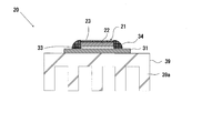
- FIG. 1 is an explanatory diagram showing an outline of the configuration of an example of the fluorescent light source device of the present invention
- FIG. 2 is an explanatory sectional view showing the configuration of a fluorescent light emitting member in the fluorescent light source device of FIG. 3 is an enlarged view for explaining the wavelength converting member in the fluorescent light emitting member of FIG. 2
- FIG. 4 is an explanatory view showing the surface structure of the photonic structure portion of the wavelength converting member of FIG. It is a fragmentary sectional view.
- the fluorescent light source device 10 includes a laser diode 11 and a fluorescent light emitting member 20 disposed to face the laser diode 11.
- the fluorescent light emitting member 20 includes a wavelength conversion member 21 that is excited by excitation light L that is laser light emitted from the laser diode 11 and emits fluorescence L1.
- a collimator lens 15 that emits the excitation light L from the incident laser diode 11 as a parallel light beam is disposed at a position between the laser diode 11 and the fluorescent light emitting member 20 close to the laser diode 11.
- a dichroic mirror 16 that transmits the excitation light L from the laser diode 11 and reflects the fluorescence L1 from the wavelength conversion member 21 is disposed between the collimator lens 15 and the fluorescent light emitting member 20. For example, it is arranged in a posture inclined at an angle of 45 °.
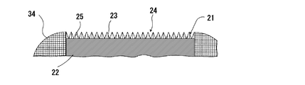
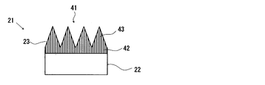
- the fluorescent light emitting member 20 has a substantially disk-shaped wavelength conversion member 21 provided on the surface (upper surface in FIG. 2) of a rectangular flat substrate 31.
- the wavelength conversion member 21 includes a disk-shaped fluorescent member 22 and a substantially circular plate formed on the surface (the upper surface in FIGS. 3 and 4) of the fluorescent member 22.
- the photonic structure part 23 is shaped.
- the surface of the photonic structure portion 23 (upper surface in FIGS. 2 to 4) is an excitation light receiving surface and a fluorescence emitting surface.
- a light reflecting film 33 made of a multilayer film is provided on the back surface of the wavelength conversion member 21, that is, the back surface of the fluorescent member 22 (the lower surface in FIG. 2).
- An annular diffuse reflection member 34 is provided on the side surface of the wavelength conversion member 21 in close contact with the side surface.
- the diffuse reflection member 34 for example, a material made of a mixture of silicone and diffusing particles such as alumina and titania, or a material obtained by drying a ceramic paste containing an alkali metal element or the like is used.
- the wavelength conversion member 21 is provided with the light reflection film 33 and the diffuse reflection member 34 to have a reflection function on the back surface and the side surface. Further, a bonding member (not shown) is interposed between the light reflection film 33 and the substrate 31, and the wavelength conversion member 21 is bonded onto the substrate 31 by the bonding member.
- a heat radiating member 39 made of a metal such as copper is disposed on the back surface of the substrate 31.
- the heat radiating member 39 is provided with heat radiating fins 39a.
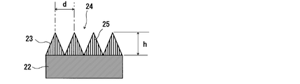
- the photonic structure portion 23 is formed by forming a periodic structure 24 in which a plurality of convex portions 25 are two-dimensionally arranged on the fluorescence emission surface, that is, the surface of the photonic structure portion 23.
- the periodic structure 24 forms a photonic structure.
- the photonic structure indicates a two-dimensional periodic structure, and specifically indicates an uneven structure in which a plurality of convex portions are two-dimensionally and periodically arranged.
- the periodic structure 24 in the photonic structure portion 23 is a two-dimensional periodic array in which the substantially conical convex portions 25 are densely packed.
- the period d is set to a size of a range (Bragg condition) in which diffraction of the fluorescence L1 emitted from the phosphor constituting the fluorescent member 22 is generated.
- the period d of the periodic structure 24 is a value obtained by dividing the peak wavelength of the fluorescence L1 emitted from the phosphor by the refractive index of the material (specifically, the inorganic compound layer) constituting the periodic structure 24. (Hereinafter referred to as “optical length”) or a value of several times the optical length.
- the period of the periodic structure means a center-to-center distance (nm) between adjacent convex portions in the periodic structure.
- the fluorescence L1 can be emitted from the surface of the wavelength conversion member 21 to the outside with high efficiency.
- an aspect ratio which is a ratio (h / d) of the height h of the convex portion 25 to the period d in the periodic structure 24 is 0.2 or more.
- the periodic structure aspect ratio is 0.2 or more.
- the surface of the photonic structure portion 23 which is the fluorescence emission surface of the wavelength conversion member 21 with high efficiency can be obtained from the fluorescence L1 emitted from the phosphor constituting the fluorescent member 22. Can be taken out from the outside.
- the periodic structure aspect ratio being 0.2 or more, reflection of the excitation light L on the surface of the photonic structure portion 23, that is, the surface of the wavelength conversion member 21 can be suppressed. Therefore, when the surface of the photonic structure portion 23 is irradiated with the excitation light L, the excitation light L can be sufficiently taken into the wavelength conversion member 21.
- the photonic structure portion 23 is made of a metal oxide, and is an inorganic compound layer (hereinafter also referred to as “specific inorganic compound layer”) having a columnar structure extending in a direction away from the fluorescent member 22 (upward in FIGS. 2 to 4). .). That is, the photonic structure portion 23 is obtained by forming the periodic structure 24 on the surface of the specific inorganic compound layer.
- the specific inorganic compound layer constituting the photonic structure portion 23 is composed of a plurality of columnar units (inorganic compound columnar units), and each of the plurality of columnar units extends in a direction away from the fluorescent member 22 and is adjacent to each other. It is a porous material in which a minute space is formed between columnar units.
- each of the some convex part 25 is comprised by the columnar unit. That is, it is preferable that the convex part 25 consists of one columnar unit.
- the convex part 25 can surely have an intended shape by a method for manufacturing a fluorescent light source device (a wavelength conversion member forming step) described later.
- the material of the specific inorganic compound layer constituting the photonic structure portion 23 include alumina (Al 2 O 3 ), hafnium oxide (HfO 2 ), magnesium oxide (MgO), tin oxide (SnO 2 ), and tungsten oxide. (WO 3 ), yttrium oxide (Y 2 O 3 ), indium tin oxide (ITO), zirconia (ZrO 2 ), tantalum oxide (Ta 2 O 5 ), titanium oxide (TiO 2 ), niobium oxide (Nb 2 O 5) And metal oxides such as zirconia (ZrO 2 ) and titanium oxide (TiO 2 ).
- zirconia thermal expansion coefficient
- zirconia thermal expansion coefficient
- it has a thermal expansion coefficient approximate to the thermal expansion coefficient (6 ⁇ 10 ⁇ 6 to 8 ⁇ 10 ⁇ 6 / K) of the phosphor (LuAG, YAG).
- 10.5 ⁇ 10 ⁇ 6 / K indium tin oxide (thermal expansion coefficient 6.8 ⁇ 10 ⁇ 6 / K) and titanium oxide (thermal expansion coefficient 7.9 ⁇ 10 ⁇ 6 / K) are preferable.
- zirconia is more preferable because of its small absorption coefficient (specifically, 13 cm ⁇ 1 (absorption coefficient for light having a wavelength of 550 nm)).
- the specific inorganic compound layer which comprises the photonic structure part 23 is a thing with a large refractive index.
- the refractive index of the specific inorganic compound layer is preferably not less than the refractive index value of the fluorescent member 22. According to the configuration of the photonic structure portion 23 with the specific inorganic compound layer whose refractive index is higher than the refractive index value of the fluorescent member 23, the fluorescence L1 incident on the interface between the fluorescent member 22 and the photonic structure portion 23 Refraction occurs by passing through the interface.
- the traveling direction of the fluorescence L1 is changed at the interface between the fluorescence member 22 and the photonic structure portion 23, the fluorescence L1 is suppressed from being confined inside the wavelength conversion member 21, and as a result, the fluorescence L1 is reduced.
- the light can be emitted from the surface of the photonic structure portion 23 to the outside with high efficiency.
- a specific inorganic compound layer having a higher refractive index than that of the fluorescent member 22 it is possible to form the periodic structure 24 having a small period d. Therefore, since the convex portion 25 constituting the periodic structure 24 can be designed with a small height even if the aspect ratio (periodic structure aspect ratio) is large, the periodic structure 24 can be easily formed.
- a soft mold can be produced and a resist pattern film can be easily formed (imprint operation).
- the thickness of the photonic structure portion 23 is, for example, 0.05 to 1.0 ⁇ m. In the example of this figure, the thickness of the photonic structure portion 23 is the height h of the convex portion 25.
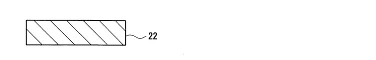
- the fluorescent member 22 contains a phosphor.
- the fluorescent member 22 is made of a single crystal or polycrystalline phosphor, or a mixture of a single crystal or polycrystalline phosphor and a ceramic binder. It consists of a knot. That is, the fluorescent member 22 is composed of a single crystal or polycrystalline phosphor.
- the sintered body of the mixture of the phosphor and the ceramic binder used as the fluorescent member 22 nano-sized alumina particles are used as the ceramic binder. This sintered body is obtained by mixing several mass% to several tens mass% ceramic binder with respect to 100 mass% of the phosphor, pressing the mixture, and then firing.
- the fluorescent member 22 is made of a single crystal or polycrystalline phosphor, the fluorescent member 22 has high thermal conductivity. Therefore, in the fluorescent member 22, since the heat generated by the irradiation of the excitation light L is efficiently exhausted, the fluorescent member 22 is suppressed from becoming high temperature.
- the single crystal phosphor constituting the fluorescent member 22 can be obtained, for example, by the Czochralski method. Specifically, the seed crystal is brought into contact with the melted raw material in the crucible, and in this state, the seed crystal is pulled up in the vertical direction while rotating the seed crystal to grow the single crystal on the seed crystal. The body is obtained.
- the polycrystalline fluorescent substance which comprises the fluorescent member 22 can be obtained as follows, for example. First, raw materials such as a base material, an activator, and a firing aid are pulverized by a ball mill or the like to obtain raw material fine particles of submicron or less. Next, using this raw material fine particles, a molded body is formed and sintered by, for example, a slip casting method. Thereafter, a polycrystalline phosphor having a porosity of 0.5% or less, for example, is obtained by subjecting the obtained sintered body to hot isostatic pressing.
- the phosphor constituting the fluorescent member 22 include YAG (Y 3 Al 5 O 12 ), LuAG, (Lu 3 Al 5 O 12 ), CASN (CaAlSiN 3 : Eu), and SCASN ((Sr, Ca). AlSiN 3 : Eu) and the like.
- the thickness of the fluorescent member 22 is, for example, 0.05 to 2.0 mm from the viewpoint of the conversion efficiency (quantum yield) of the excitation light L into the fluorescent light L1 and the exhaust heat.
- the substrate 31 As a material constituting the substrate 31, an aluminum substrate or the like via a heat radiation adhesive in which metal fine powder is mixed into a resin can be used.
- the thickness of the substrate 31 is, for example, 0.5 to 1.0 mm.
- the fluorescent light source device 10 having the above-described configuration can be manufactured by, for example, obtaining the wavelength conversion member 21 through a specific process described below. Specifically, the wavelength conversion member 21 forms an inorganic compound layer having a columnar structure extending in a direction away from the fluorescent member 22 on the fluorescent member 22 and etches the surface of the inorganic compound layer (hereinafter, referred to as “a”). It is also referred to as “wavelength conversion member forming step”).
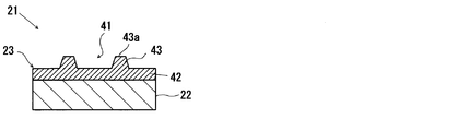
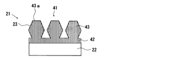
- the wavelength conversion member 21 obtained through the wavelength conversion member forming step shown in FIGS. 5 to 11 has a configuration of the photonic structure portion 23 according to FIG. Is different. That is, in the wavelength conversion member 21 according to FIG. 11, the photonic structure portion 23 is configured by a thin film portion 42 and a plurality of (two in FIG. 11) convex portions 43 provided on the thin film portion 42. ing. Further, the plurality of convex portions 43 have a truncated cone shape, and the plurality of convex portions 43 are arranged at regular intervals in a state of being separated from each other. The thin film portion 42 and the plurality of convex portions 43 form a periodic structure 41 in which the plurality of convex portions 43 are two-dimensionally arranged on the surface of the photonic structure portion 23 (upper surface in FIG. 11). Yes.
- the fluorescent member 22 is prepared and washed with an organic solvent.
- the fluorescent member 22 has a circular flat plate shape with a diameter of 50.8 mm and a thickness of 0.13 mm, and the front and back surfaces are polished.
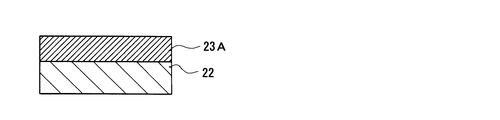
- an inorganic compound layer (hereinafter referred to as “photonic structure portion forming layer”) for forming the photonic structure portion 23 on the entire surface of the fluorescent member 22 (upper surface in FIG. 6).
- the photonic structure portion forming layer 23A is an inorganic compound layer made of a metal oxide and having a columnar structure extending in a direction away from the fluorescent member 22, and has a substantially flat surface (upper surface in FIG. 6).
- a sputtering method is preferably used as a sputtering method.
- the form of the obtained sputtered film can be controlled by adjusting the sputtering conditions, so that the photonic structure portion forming layer 23A having the desired columnar structure can be easily obtained.
- the sputtering method is a concept including a reactive sputtering method.
- a reactive sputtering apparatus is used.
- the columnar unit forming the photonic structure portion forming layer 23A has a ratio of the vertical width to the horizontal width (hereinafter also referred to as “columnar unit aspect ratio”). .3 or more is preferable. Since the columnar unit aspect ratio is in the above range, the photonic structure portion forming layer 23A has further improved workability by an etching method, and thus the photonic structure portion 23 has an intended shape. Can be.
- the sputtering conditions it is necessary to control the sputtering conditions. Specifically, it is preferable to reduce the high-frequency power applied between the fluorescent member 22 and the target material and reduce the flow rate of the inert gas. By reducing the applied high frequency power, the temperature of the fluorescent member 22 can be lowered when the sputtered film is formed. Therefore, recrystallization in the sputtered film formed on the fluorescent member 22 can be suppressed, and the resulting sputtered film can have the intended columnar structure.
- the sputtered film formed on the fluorescent member 22 is dense, specifically, the columnar unit aspect ratio is large, and a fine space is formed between the columnar units. And a high refractive index.
- the high frequency power applied between the fluorescent member 22 and the target material is 450 W or less.
- it is 250 W or less.
- the flow rate of an inert gas such as argon gas is preferably 1 to 20 sccm.
- the flow rate of the oxygen gas introduced together with the inert gas as necessary is preferably 0.1 to 3 sccm.
- the photonic structure portion forming layer 23A is made of a zirconia sputtered film and has a thickness of about 600 nm (specifically, 550 nm).
- the photonic structure portion forming layer 23A is formed by using a sputtering apparatus, using zirconia as a target material, high-frequency power of 250 W, an argon gas flow rate of 20 sccm, and an oxygen gas flow rate of 0.5 sccm as an inert gas. Depending on conditions, it was formed over 4 hours.
- the temperature (surface temperature) of the fluorescent member 22 was 100 ° C. or lower.
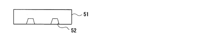
- a resist film is obtained on the surface (upper surface in FIG. 6) of the photonic structure portion forming layer 23A formed on the fluorescent member 22 by, for example, a spin coating method, and this resist film is patterned by the nanoimprint method.
- a pattern corresponding to the periodic structure 41 in the photonic structure portion 23 to be formed (specifically, a plurality of concave portions 52 are arranged).
- a soft mold 51 having a pattern) is formed.
- the soft mold 51 for example, one made of a thermosetting material or one made of an ultraviolet curable material is used.
- the nanoimprint apparatus as shown in FIG. 8, the soft mold 51 is pressed against the resist film formed on the photonic structure portion forming layer 23 ⁇ / b> A, whereby the pattern formed on the soft mold 51 is formed on the resist film. Transcript.
- FIG. 7 a pattern corresponding to the periodic structure 41 in the photonic structure portion 23 to be formed (specifically, a plurality of concave portions 52 are arranged).
- a soft mold 51 having a pattern) is formed.
- the soft mold 51 for example, one made of a thermosetting material or one made of an ultraviolet curable material is used.
- the nanoimprint apparatus as shown in FIG. 8
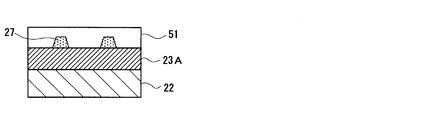
- a resist pattern film 27 with a period of 460 nm is formed on the photonic structure portion forming layer 23A.
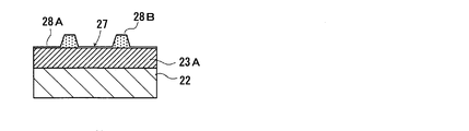
- the resist pattern film 27 is formed so as to cover the entire surface of the photonic structure portion forming layer 23A, a thin film portion 28A formed on the surface of the photonic structure portion forming layer 23A, and this A plurality of convex portions 28B formed on the thin film portion 28A.
- the plurality of protrusions 28B have a constant interval (period (distance between the centers of the protrusions 28B) corresponding to the protrusions 43 constituting the periodic structure 41 of the photonic structure part 23 to be formed is 460 nm, etc. (Interval).
- the periodic structure 41 is formed on the surface (upper surface in FIG. 10) as shown in FIG.
- the photonic structure part 23 having is obtained.
- a specific example of the dry etching method is an ICP (Inductive Coupling Plasma) etching method.
- the formation conditions for forming the periodic structure 41 by this ICP etching method are as necessary or necessary depending on the shape of the periodic structure 41 (specifically, for example, the shape of the convex portion 43 and the periodic structure aspect ratio). Accordingly, the thickness is appropriately determined in consideration of the material of the photonic structure portion forming layer 23A, the columnar unit aspect ratio, and the like.
- the etching gas for example, a gas such as silane gas (SiH 4 ), silicon tetrafluoride gas (SiF 4 ), diborane gas (B 2 H 6 ), and boron trichloride gas (BCl 3 ) is used.
- the high frequency power is set to 100 to 700 W
- the bias power is set to 1 to 30 W.
- the periodic structure 41 of the photonic structure portion 23 is formed by using boron trichloride gas (BCl 3 ) as an etching gas by an ICP etching method, with a high-frequency power of 700 W and a bias power of 20 W. It is formed with a processing time of 350 seconds.
- the remaining film 27A of the resist pattern film 27 left on the formed photonic structure portion 23 is removed with an organic solvent, thereby obtaining the wavelength conversion member 21 having the configuration shown in FIG.
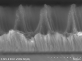
- the SEM photograph of the obtained wavelength conversion member 21 is shown in FIG.
- the columnar unit aspect ratio of the wavelength conversion member 21 was 9.3.
- the fluorescent light source device 10 is manufactured by arranging the light emitting member 20, the laser diode 11, and other components at appropriate positions.
- the excitation light L which is laser light emitted from the laser diode 11, is collimated by the collimator lens 15. Thereafter, the excitation light L passes through the dichroic mirror 16 and is irradiated substantially perpendicularly to the excitation light receiving surface of the wavelength conversion member 21 in the fluorescent light emitting member 20, that is, the surface of the photonic structure portion 23. The light enters the fluorescent member 22 through the portion 23. And in the fluorescent member 22, the fluorescent substance which comprises the said fluorescent member 22 is excited. Thereby, in the fluorescent member 22, fluorescence L1 is radiated
- the wavelength conversion member 21 is formed by forming the photonic structure portion 23 on the surface of the fluorescence member 22, and the excitation light receiving surface and the fluorescence emission are formed by the surface of the photonic structure portion 23.
- the surface is configured.
- a periodic structure 24 is formed in which substantially conical convex portions 25 are two-dimensionally arranged. Therefore, the fluorescence L1 radiated from the phosphor constituting the fluorescent member 22 can be taken out from the surface of the photonic structure portion 23 that is the fluorescent emission surface of the wavelength conversion member 21 with high efficiency.
- the fluorescence L1 can be extracted from the wavelength conversion member 21 with high efficiency, the fluorescence member 22 is suppressed from being heated by the fluorescence L1 that cannot be emitted from the fluorescence emission surface. Therefore, since the temperature rise of the fluorescent member 22 is suppressed, it is possible to suppress a decrease in the amount of fluorescent light resulting from the occurrence of temperature quenching in the phosphor.
- the material of the photonic structure portion 23 is an inorganic compound (metal oxide), the shape thereof is not deformed by the influence of heat such as the heat of the laser light that is the excitation light L. Therefore, in the wavelength conversion member 21, the fluorescence L1 can be extracted with high efficiency from the fluorescence emission surface over a long period of time. Therefore, according to the fluorescent light source device 10, since the fluorescence L1 generated inside the wavelength conversion member 21 can be effectively used and emitted to the outside with high efficiency, high luminous efficiency can be obtained.
- the wavelength conversion member 21 is composed of the fluorescent member 22 and the photonic structure portion 23, it is not necessary for the fluorescent member 22 to have a periodic structure. And the specific inorganic compound layer which comprises the photonic structure part 23 has the outstanding workability (workability). Therefore, the periodic structure 24 having the desired shape can be easily formed through the wavelength conversion member forming step.
- the wavelength converting member may be any member as long as the photonic structure portion formed on the fluorescent member is composed of a specific inorganic compound layer, and the photonic structure (periodic structure) in the photonic structure portion is shown in FIGS. It is not limited to the periodic structure according to FIG. Specifically, the wavelength conversion member may have a structure as shown in FIG. 11 and FIGS. Specifically, the photonic structure portion 23 according to FIG. 13 includes a thin film portion 42 provided on the surface of the fluorescent member 22 and a plurality (four in FIG. 13) of weights provided on the thin film portion 42.
- the photonic structure portion 23 has the same configuration as that of the photonic structure portion 23 shown in FIG. 1 except that it is constituted by a convex portion 43 (for example, substantially conical).
- the photonic structure portion 23 according to FIG. 14 has the same configuration as the photonic structure portion 23 according to FIG. 13 except that the shape of the convex portion 43 is a frustum shape (for example, a truncated cone shape). is there.
- the convex portion 43 has a hexagonal cross-sectional shape in the height direction of the convex portion 43, and the plurality of convex portions 43 are constant in a state of being separated from each other.
- the photonic structure portion 23 has the same configuration as the photonic structure portion 23 shown in FIG.
- the cross-sectional shape in the direction perpendicular to the height direction of the convex portion 43 is circular.
- the dimension (maximum dimension) of the tip portion 43a. Is less than the wavelength of the excitation light L.
- the wavelength conversion member should just be that the fluorescence emission surface in the wavelength conversion member was formed by the surface of the photonic structure part, and the excitation light receiving surface in the wavelength conversion member was formed by the back surface of the fluorescence member, for example There may be.
- the structure of the whole fluorescence light source device is not limited to what is shown in FIG. 1, A various structure is employable.
- the fluorescent light source device according to FIG. 1 the light of one laser diode 11 is used, but there are a plurality of laser diodes, a condensing lens is arranged in front of the wavelength conversion member, and the condensed light is emitted at the wavelength.
- the form which irradiates a conversion member may be sufficient.
- the excitation light is not limited to the light from the laser diode, but may be the one that collects the light from the LED as long as it can excite the phosphor in the wavelength conversion member, and further, mercury, xenon, etc. May be light from a sealed lamp.
- the wavelength of the excitation light is the main emission wavelength region.
- the present invention is not limited to this.
Landscapes
- Engineering & Computer Science (AREA)
- General Engineering & Computer Science (AREA)
- Physics & Mathematics (AREA)
- Spectroscopy & Molecular Physics (AREA)
- Optics & Photonics (AREA)
- Microelectronics & Electronic Packaging (AREA)
- Led Device Packages (AREA)
- Semiconductor Lasers (AREA)
- Luminescent Compositions (AREA)
- Investigating, Analyzing Materials By Fluorescence Or Luminescence (AREA)
- Condensed Matter Physics & Semiconductors (AREA)
- General Physics & Mathematics (AREA)
- Electromagnetism (AREA)
Priority Applications (2)
| Application Number | Priority Date | Filing Date | Title |
|---|---|---|---|
| US15/023,142 US10047919B2 (en) | 2013-09-20 | 2014-09-11 | Fluorescent light source device, and method for manufacturing same |
| CN201480051629.7A CN105556201B (zh) | 2013-09-20 | 2014-09-11 | 荧光光源装置及其制造方法 |
Applications Claiming Priority (2)
| Application Number | Priority Date | Filing Date | Title |
|---|---|---|---|
| JP2013195292A JP6166628B2 (ja) | 2013-09-20 | 2013-09-20 | 蛍光光源装置およびその製造方法 |
| JP2013-195292 | 2013-09-20 |
Publications (1)
| Publication Number | Publication Date |
|---|---|
| WO2015041138A1 true WO2015041138A1 (ja) | 2015-03-26 |
Family
ID=52688789
Family Applications (1)
| Application Number | Title | Priority Date | Filing Date |
|---|---|---|---|
| PCT/JP2014/074092 Ceased WO2015041138A1 (ja) | 2013-09-20 | 2014-09-11 | 蛍光光源装置およびその製造方法 |
Country Status (4)
| Country | Link |
|---|---|
| US (1) | US10047919B2 (enExample) |
| JP (1) | JP6166628B2 (enExample) |
| CN (1) | CN105556201B (enExample) |
| WO (1) | WO2015041138A1 (enExample) |
Families Citing this family (8)
| Publication number | Priority date | Publication date | Assignee | Title |
|---|---|---|---|---|
| JP2017107071A (ja) * | 2015-12-10 | 2017-06-15 | 日本電気硝子株式会社 | 波長変換部材及び波長変換素子、並びにそれらを用いた発光装置 |
| EP3475988B1 (en) | 2016-06-22 | 2022-08-10 | Lumileds LLC | Lighting system |
| JP6365656B2 (ja) * | 2016-12-28 | 2018-08-01 | ウシオ電機株式会社 | 蛍光光源装置およびその製造方法 |
| KR101984102B1 (ko) | 2017-11-03 | 2019-05-30 | 엘지전자 주식회사 | 형광체 모듈 |
| DE102019108995A1 (de) * | 2019-04-05 | 2020-10-08 | HELLA GmbH & Co. KGaA | Beleuchtungsvorrichtung für Fahrzeuge |
| JP7439592B2 (ja) | 2020-03-18 | 2024-02-28 | セイコーエプソン株式会社 | 波長変換素子、光源装置およびプロジェクター |
| WO2023110396A1 (en) * | 2021-12-14 | 2023-06-22 | Signify Holding B.V. | High brightness light source |
| CN114813675A (zh) * | 2022-04-13 | 2022-07-29 | 苏州紫翔电子科技有限公司 | Fpc的识别和检测方法和fpc的识别和检测装置 |
Citations (3)
| Publication number | Priority date | Publication date | Assignee | Title |
|---|---|---|---|---|
| JP2004294566A (ja) * | 2003-03-25 | 2004-10-21 | Univ Shinshu | フォトニック結晶 |
| JP2008060092A (ja) * | 2005-01-31 | 2008-03-13 | Sharp Corp | 光機能性膜およびその製造方法 |
| JP2009175238A (ja) * | 2008-01-22 | 2009-08-06 | Seiko Epson Corp | 光学素子及び光源ユニット |
Family Cites Families (6)
| Publication number | Priority date | Publication date | Assignee | Title |
|---|---|---|---|---|
| WO2006110535A2 (en) * | 2005-04-07 | 2006-10-19 | Nanometrics Incorporated | Apparatus and methods for scatterometry of optical devices |
| CN101261901B (zh) * | 2008-04-29 | 2010-06-02 | 四川大学 | 一种染料敏化太阳能电池阳极及其制备方法 |
| US20110216550A1 (en) | 2010-03-02 | 2011-09-08 | Teruo Koike | Vehicle light |
| JP5510646B2 (ja) | 2010-03-18 | 2014-06-04 | スタンレー電気株式会社 | 車両用灯具 |
| WO2012108384A1 (ja) * | 2011-02-10 | 2012-08-16 | シャープ株式会社 | 蛍光体基板、およびこれを用いた表示装置、照明装置 |
| JP2012243624A (ja) * | 2011-05-20 | 2012-12-10 | Stanley Electric Co Ltd | 光源装置および照明装置 |
-
2013
- 2013-09-20 JP JP2013195292A patent/JP6166628B2/ja active Active
-
2014
- 2014-09-11 US US15/023,142 patent/US10047919B2/en active Active
- 2014-09-11 CN CN201480051629.7A patent/CN105556201B/zh active Active
- 2014-09-11 WO PCT/JP2014/074092 patent/WO2015041138A1/ja not_active Ceased
Patent Citations (3)
| Publication number | Priority date | Publication date | Assignee | Title |
|---|---|---|---|---|
| JP2004294566A (ja) * | 2003-03-25 | 2004-10-21 | Univ Shinshu | フォトニック結晶 |
| JP2008060092A (ja) * | 2005-01-31 | 2008-03-13 | Sharp Corp | 光機能性膜およびその製造方法 |
| JP2009175238A (ja) * | 2008-01-22 | 2009-08-06 | Seiko Epson Corp | 光学素子及び光源ユニット |
Also Published As
| Publication number | Publication date |
|---|---|
| CN105556201B (zh) | 2017-09-22 |
| JP2015060789A (ja) | 2015-03-30 |
| US20160230945A1 (en) | 2016-08-11 |
| JP6166628B2 (ja) | 2017-07-19 |
| CN105556201A (zh) | 2016-05-04 |
| US10047919B2 (en) | 2018-08-14 |
Similar Documents
| Publication | Publication Date | Title |
|---|---|---|
| JP6166628B2 (ja) | 蛍光光源装置およびその製造方法 | |
| JP6489829B2 (ja) | 蛍光光源装置 | |
| JP6356522B2 (ja) | 蛍光発光部材およびその製造方法並びに蛍光光源装置 | |
| JP6111960B2 (ja) | 蛍光光源装置 | |
| JP6580133B2 (ja) | パターニングされた薄膜波長変換器の製造方法 | |
| JP6107190B2 (ja) | 蛍光光源装置 | |
| JP2015195098A (ja) | 蛍光光源装置 | |
| JP2014082401A (ja) | 蛍光光源装置 | |
| JP5971148B2 (ja) | 蛍光光源装置 | |
| US10208900B2 (en) | Fluorescence light source device with wavelength conversion member with particular ratio between light transmission percentage and light reflection percentage | |
| JP2015060789A5 (enExample) | ||
| JP2016031838A5 (ja) | 蛍光発光部材およびその製造方法並びに蛍光光源装置 | |
| CN110073143A (zh) | 荧光光源装置及其制造方法 | |
| WO2015141376A1 (ja) | 蛍光光源装置 | |
| JP2013069547A (ja) | 放熱基板及びその製造方法並びにその放熱基板を用いた光半導体装置 | |
| JP2016194697A (ja) | 蛍光光源装置 | |
| JP2015038978A (ja) | 波長変換部材 | |
| JP2016178087A (ja) | 蛍光光源装置 | |
| WO2015045976A1 (ja) | 蛍光光源装置 | |
| JP2018113117A (ja) | 蛍光光源装置およびその製造方法 | |
| JP6557784B2 (ja) | 照明装置の変換体 | |
| WO2017175635A1 (ja) | 蛍光光源装置 | |
| JP6747285B2 (ja) | 発光素子、蛍光光源装置 |
Legal Events
| Date | Code | Title | Description |
|---|---|---|---|
| WWE | Wipo information: entry into national phase |
Ref document number: 201480051629.7 Country of ref document: CN |
|
| 121 | Ep: the epo has been informed by wipo that ep was designated in this application |
Ref document number: 14845569 Country of ref document: EP Kind code of ref document: A1 |
|
| WWE | Wipo information: entry into national phase |
Ref document number: 15023142 Country of ref document: US |
|
| NENP | Non-entry into the national phase |
Ref country code: DE |
|
| 122 | Ep: pct application non-entry in european phase |
Ref document number: 14845569 Country of ref document: EP Kind code of ref document: A1 |