WO2015041012A1 - 制御装置、動的バックライト制御プログラムおよび制御装置の制御方法 - Google Patents
制御装置、動的バックライト制御プログラムおよび制御装置の制御方法 Download PDFInfo
- Publication number
- WO2015041012A1 WO2015041012A1 PCT/JP2014/072306 JP2014072306W WO2015041012A1 WO 2015041012 A1 WO2015041012 A1 WO 2015041012A1 JP 2014072306 W JP2014072306 W JP 2014072306W WO 2015041012 A1 WO2015041012 A1 WO 2015041012A1
- Authority
- WO
- WIPO (PCT)
- Prior art keywords
- image
- pixel
- display
- display screen
- control
- Prior art date
- Legal status (The legal status is an assumption and is not a legal conclusion. Google has not performed a legal analysis and makes no representation as to the accuracy of the status listed.)
- Ceased
Links
Images


Classifications
-
- G—PHYSICS
- G09—EDUCATION; CRYPTOGRAPHY; DISPLAY; ADVERTISING; SEALS
- G09G—ARRANGEMENTS OR CIRCUITS FOR CONTROL OF INDICATING DEVICES USING STATIC MEANS TO PRESENT VARIABLE INFORMATION
- G09G3/00—Control arrangements or circuits, of interest only in connection with visual indicators other than cathode-ray tubes
- G09G3/20—Control arrangements or circuits, of interest only in connection with visual indicators other than cathode-ray tubes for presentation of an assembly of a number of characters, e.g. a page, by composing the assembly by combination of individual elements arranged in a matrix no fixed position being assigned to or needed to be assigned to the individual characters or partial characters
- G09G3/34—Control arrangements or circuits, of interest only in connection with visual indicators other than cathode-ray tubes for presentation of an assembly of a number of characters, e.g. a page, by composing the assembly by combination of individual elements arranged in a matrix no fixed position being assigned to or needed to be assigned to the individual characters or partial characters by control of light from an independent source
- G09G3/3406—Control of illumination source
-
- G—PHYSICS
- G09—EDUCATION; CRYPTOGRAPHY; DISPLAY; ADVERTISING; SEALS
- G09G—ARRANGEMENTS OR CIRCUITS FOR CONTROL OF INDICATING DEVICES USING STATIC MEANS TO PRESENT VARIABLE INFORMATION
- G09G3/00—Control arrangements or circuits, of interest only in connection with visual indicators other than cathode-ray tubes
- G09G3/20—Control arrangements or circuits, of interest only in connection with visual indicators other than cathode-ray tubes for presentation of an assembly of a number of characters, e.g. a page, by composing the assembly by combination of individual elements arranged in a matrix no fixed position being assigned to or needed to be assigned to the individual characters or partial characters
- G09G3/34—Control arrangements or circuits, of interest only in connection with visual indicators other than cathode-ray tubes for presentation of an assembly of a number of characters, e.g. a page, by composing the assembly by combination of individual elements arranged in a matrix no fixed position being assigned to or needed to be assigned to the individual characters or partial characters by control of light from an independent source
- G09G3/36—Control arrangements or circuits, of interest only in connection with visual indicators other than cathode-ray tubes for presentation of an assembly of a number of characters, e.g. a page, by composing the assembly by combination of individual elements arranged in a matrix no fixed position being assigned to or needed to be assigned to the individual characters or partial characters by control of light from an independent source using liquid crystals
- G09G3/3611—Control of matrices with row and column drivers
- G09G3/3614—Control of polarity reversal in general
-
- G—PHYSICS
- G09—EDUCATION; CRYPTOGRAPHY; DISPLAY; ADVERTISING; SEALS
- G09G—ARRANGEMENTS OR CIRCUITS FOR CONTROL OF INDICATING DEVICES USING STATIC MEANS TO PRESENT VARIABLE INFORMATION
- G09G3/00—Control arrangements or circuits, of interest only in connection with visual indicators other than cathode-ray tubes
- G09G3/20—Control arrangements or circuits, of interest only in connection with visual indicators other than cathode-ray tubes for presentation of an assembly of a number of characters, e.g. a page, by composing the assembly by combination of individual elements arranged in a matrix no fixed position being assigned to or needed to be assigned to the individual characters or partial characters
- G09G3/34—Control arrangements or circuits, of interest only in connection with visual indicators other than cathode-ray tubes for presentation of an assembly of a number of characters, e.g. a page, by composing the assembly by combination of individual elements arranged in a matrix no fixed position being assigned to or needed to be assigned to the individual characters or partial characters by control of light from an independent source
- G09G3/36—Control arrangements or circuits, of interest only in connection with visual indicators other than cathode-ray tubes for presentation of an assembly of a number of characters, e.g. a page, by composing the assembly by combination of individual elements arranged in a matrix no fixed position being assigned to or needed to be assigned to the individual characters or partial characters by control of light from an independent source using liquid crystals
- G09G3/3611—Control of matrices with row and column drivers
- G09G3/3618—Control of matrices with row and column drivers with automatic refresh of the display panel using sense/write circuits
-
- G—PHYSICS
- G09—EDUCATION; CRYPTOGRAPHY; DISPLAY; ADVERTISING; SEALS
- G09G—ARRANGEMENTS OR CIRCUITS FOR CONTROL OF INDICATING DEVICES USING STATIC MEANS TO PRESENT VARIABLE INFORMATION
- G09G3/00—Control arrangements or circuits, of interest only in connection with visual indicators other than cathode-ray tubes
- G09G3/20—Control arrangements or circuits, of interest only in connection with visual indicators other than cathode-ray tubes for presentation of an assembly of a number of characters, e.g. a page, by composing the assembly by combination of individual elements arranged in a matrix no fixed position being assigned to or needed to be assigned to the individual characters or partial characters
- G09G3/34—Control arrangements or circuits, of interest only in connection with visual indicators other than cathode-ray tubes for presentation of an assembly of a number of characters, e.g. a page, by composing the assembly by combination of individual elements arranged in a matrix no fixed position being assigned to or needed to be assigned to the individual characters or partial characters by control of light from an independent source
- G09G3/36—Control arrangements or circuits, of interest only in connection with visual indicators other than cathode-ray tubes for presentation of an assembly of a number of characters, e.g. a page, by composing the assembly by combination of individual elements arranged in a matrix no fixed position being assigned to or needed to be assigned to the individual characters or partial characters by control of light from an independent source using liquid crystals
- G09G3/3611—Control of matrices with row and column drivers
- G09G3/3696—Generation of voltages supplied to electrode drivers
-
- G—PHYSICS
- G09—EDUCATION; CRYPTOGRAPHY; DISPLAY; ADVERTISING; SEALS
- G09G—ARRANGEMENTS OR CIRCUITS FOR CONTROL OF INDICATING DEVICES USING STATIC MEANS TO PRESENT VARIABLE INFORMATION
- G09G5/00—Control arrangements or circuits for visual indicators common to cathode-ray tube indicators and other visual indicators
- G09G5/02—Control arrangements or circuits for visual indicators common to cathode-ray tube indicators and other visual indicators characterised by the way in which colour is displayed
- G09G5/06—Control arrangements or circuits for visual indicators common to cathode-ray tube indicators and other visual indicators characterised by the way in which colour is displayed using colour palettes, e.g. look-up tables
-
- G—PHYSICS
- G09—EDUCATION; CRYPTOGRAPHY; DISPLAY; ADVERTISING; SEALS
- G09G—ARRANGEMENTS OR CIRCUITS FOR CONTROL OF INDICATING DEVICES USING STATIC MEANS TO PRESENT VARIABLE INFORMATION
- G09G2300/00—Aspects of the constitution of display devices
- G09G2300/04—Structural and physical details of display devices
- G09G2300/0469—Details of the physics of pixel operation
- G09G2300/0478—Details of the physics of pixel operation related to liquid crystal pixels
-
- G—PHYSICS
- G09—EDUCATION; CRYPTOGRAPHY; DISPLAY; ADVERTISING; SEALS
- G09G—ARRANGEMENTS OR CIRCUITS FOR CONTROL OF INDICATING DEVICES USING STATIC MEANS TO PRESENT VARIABLE INFORMATION
- G09G2320/00—Control of display operating conditions
- G09G2320/02—Improving the quality of display appearance
- G09G2320/0233—Improving the luminance or brightness uniformity across the screen
-
- G—PHYSICS
- G09—EDUCATION; CRYPTOGRAPHY; DISPLAY; ADVERTISING; SEALS
- G09G—ARRANGEMENTS OR CIRCUITS FOR CONTROL OF INDICATING DEVICES USING STATIC MEANS TO PRESENT VARIABLE INFORMATION
- G09G2320/00—Control of display operating conditions
- G09G2320/02—Improving the quality of display appearance
- G09G2320/0247—Flicker reduction other than flicker reduction circuits used for single beam cathode-ray tubes
-
- G—PHYSICS
- G09—EDUCATION; CRYPTOGRAPHY; DISPLAY; ADVERTISING; SEALS
- G09G—ARRANGEMENTS OR CIRCUITS FOR CONTROL OF INDICATING DEVICES USING STATIC MEANS TO PRESENT VARIABLE INFORMATION
- G09G2320/00—Control of display operating conditions
- G09G2320/02—Improving the quality of display appearance
- G09G2320/0261—Improving the quality of display appearance in the context of movement of objects on the screen or movement of the observer relative to the screen
-
- G—PHYSICS
- G09—EDUCATION; CRYPTOGRAPHY; DISPLAY; ADVERTISING; SEALS
- G09G—ARRANGEMENTS OR CIRCUITS FOR CONTROL OF INDICATING DEVICES USING STATIC MEANS TO PRESENT VARIABLE INFORMATION
- G09G2320/00—Control of display operating conditions
- G09G2320/06—Adjustment of display parameters
- G09G2320/0613—The adjustment depending on the type of the information to be displayed
-
- G—PHYSICS
- G09—EDUCATION; CRYPTOGRAPHY; DISPLAY; ADVERTISING; SEALS
- G09G—ARRANGEMENTS OR CIRCUITS FOR CONTROL OF INDICATING DEVICES USING STATIC MEANS TO PRESENT VARIABLE INFORMATION
- G09G2320/00—Control of display operating conditions
- G09G2320/06—Adjustment of display parameters
- G09G2320/0613—The adjustment depending on the type of the information to be displayed
- G09G2320/062—Adjustment of illumination source parameters
-
- G—PHYSICS
- G09—EDUCATION; CRYPTOGRAPHY; DISPLAY; ADVERTISING; SEALS
- G09G—ARRANGEMENTS OR CIRCUITS FOR CONTROL OF INDICATING DEVICES USING STATIC MEANS TO PRESENT VARIABLE INFORMATION
- G09G2320/00—Control of display operating conditions
- G09G2320/06—Adjustment of display parameters
- G09G2320/0626—Adjustment of display parameters for control of overall brightness
- G09G2320/0646—Modulation of illumination source brightness and image signal correlated to each other
-
- G—PHYSICS
- G09—EDUCATION; CRYPTOGRAPHY; DISPLAY; ADVERTISING; SEALS
- G09G—ARRANGEMENTS OR CIRCUITS FOR CONTROL OF INDICATING DEVICES USING STATIC MEANS TO PRESENT VARIABLE INFORMATION
- G09G2320/00—Control of display operating conditions
- G09G2320/10—Special adaptations of display systems for operation with variable images
- G09G2320/103—Detection of image changes, e.g. determination of an index representative of the image change
-
- G—PHYSICS
- G09—EDUCATION; CRYPTOGRAPHY; DISPLAY; ADVERTISING; SEALS
- G09G—ARRANGEMENTS OR CIRCUITS FOR CONTROL OF INDICATING DEVICES USING STATIC MEANS TO PRESENT VARIABLE INFORMATION
- G09G2330/00—Aspects of power supply; Aspects of display protection and defect management
- G09G2330/02—Details of power systems and of start or stop of display operation
- G09G2330/021—Power management, e.g. power saving
- G09G2330/022—Power management, e.g. power saving in absence of operation, e.g. no data being entered during a predetermined time
-
- G—PHYSICS
- G09—EDUCATION; CRYPTOGRAPHY; DISPLAY; ADVERTISING; SEALS
- G09G—ARRANGEMENTS OR CIRCUITS FOR CONTROL OF INDICATING DEVICES USING STATIC MEANS TO PRESENT VARIABLE INFORMATION
- G09G2340/00—Aspects of display data processing
- G09G2340/04—Changes in size, position or resolution of an image
- G09G2340/0407—Resolution change, inclusive of the use of different resolutions for different screen areas
- G09G2340/0435—Change or adaptation of the frame rate of the video stream
Definitions
- the present invention relates to a control device, a dynamic backlight control program, and a control method for the control device.
- liquid crystal display panel (hereinafter abbreviated as an oxide semiconductor liquid crystal panel) in which a TFT (thin film transistor) is formed by an oxide semiconductor using indium (In), gallium (Ga), and zinc (Zn).
- a liquid crystal display panel with high charge retention characteristics can be realized by utilizing the ON / OFF characteristics of the TFT, and a long refresh interval (low refresh rate drive) can be achieved.
- a display device with low power (hereinafter referred to as “liquid crystal display device”) can be realized.
- DBC Dynamic Backlight Control
- Japanese Patent Publication Japanese Patent Laid-Open No. 2008-83604 (published April 10, 2008)”
- oxide semiconductor liquid crystal panel and DBC are both technologies (or devices) that reduce power consumption.
- these are simply combined, if one operation is improved, it is negative with respect to the other operation.
- DBC in order to reduce display flicker due to rapid image processing and rapid backlight control (hereinafter simply referred to as “BL control”), it is necessary to perform control over a plurality of frame images in stages. For this reason, it is preferable that the number of frame images subjected to DBC is as large as possible.
- the present invention has been made in view of the above problems, and is DBC for a display device capable of low refresh rate driving such as a display device using a liquid crystal panel in which an oxide semiconductor is used for a semiconductor layer of a TFT. It is an object of the present invention to provide a control device or the like that can suppress the deterioration of the power consumption reduction effect when processing is enabled.
- a control device is a control device for a display device that can be driven at a low refresh rate, and has been updated in response to a request to update display screen display.
- An image analysis unit that determines whether an image is a still image or a moving image, and if it is determined that the image is a moving image, the pixel value of each pixel of the display screen that displays the image is higher than before the determination.
- An image processing unit that performs control to change, and a backlight control unit that performs control to lower the luminance of the backlight in comparison with the determination before the pixel value of each pixel of the image. It is characterized by.
- a control method for a control device is a control method for a control device for a display device capable of low refresh rate driving, and the display screen display update request Determining whether the image updated in response to the image is a still image or a moving image, and if it is determined that the image is a moving image, the pixel value of each pixel of the display screen displaying the image is determined as described above A step of changing the brightness higher than before, and a step of lowering the luminance of the backlight more than before the determination in accordance with the change of the pixel value of each pixel of the display screen displaying the image. To do.
- Embodiments of the present invention will be described with reference to FIGS. 1 to 5 as follows. Descriptions of configurations other than those described in the following specific embodiments may be omitted as necessary, but are the same as those configurations when described in other embodiments. For convenience of explanation, members having the same functions as those shown in each embodiment are given the same reference numerals, and the explanation thereof is omitted as appropriate.
- a liquid crystal display device using a liquid crystal panel in which an oxide semiconductor is used for a semiconductor layer of a TFT is described as an example of the display device.
- the display device is not limited to this, The present invention can be applied to any display device capable of refresh rate driving.
- FIG. 1 is a block diagram showing a configuration of a liquid crystal display device 1 according to the present embodiment.
- the liquid crystal display device 1 includes a host control unit 2, a DBC circuit (control device) 3, and a display unit (display device) 4.
- DBC Dynamic Backlight Control
- BL luminance of the backlight
- the host control unit 2 generates image data of one frame (one frame) of frame images (hereinafter simply referred to as “update image”) that is updated in response to an update request from an application or an update request from the outside.
- the generated image data is temporarily stored and transferred to the DBC circuit 3 as necessary. Therefore, the host control unit 2 includes an image generation unit 21, a CPU 22, a temporary recording recording unit (recording unit) 23, a TG 24 (timing generator), and a screen update detection unit 25.
- the host control unit 2 is composed of a control circuit formed on a substrate, for example.
- the image generation unit 21 generates image data of an update image in response to an update request from the outside. For example, when (1) an application that is activated and executed in the liquid crystal display device 1 requests (notifies) the display generation to be updated, (2) the user of the liquid crystal display device 1 operates the input unit. When the image generation unit 21 is requested to update the display via the Internet, (3) the image of the updated image is displayed when the image generation unit 21 is notified of the display update by data streaming or broadcast waves via the Internet. Generate data. Further, when the image generation unit 21 generates the image data of the update image, the image generation unit 21 notifies the screen update detection unit 25 to that effect (update notification). The detection of the image update by the screen update detection unit 25 is not limited to such a form. For example, it may be configured to directly detect that there has been an update request from the application described above.
- the CPU 22 performs control to acquire image data of a frame image (updated image) for one screen whose display is updated from the image generation unit 21 and store it in the temporary recording unit 23.
- the TG 24 acquires the image data of the updated image from the temporary recording unit 23 according to the control of the CPU 22 and transfers it to the DBC circuit 3. Further, the TG 24 transfers at least one additional frame image, which is the same image data as that of the updated image and is used for DBC described later, to the DBC circuit 3 under the control of the CPU 22. Further, the TG 24 is image data obtained by reversing the polarity of the voltage applied to the electrodes of the respective pixels of the display panel 42 (display screen) to display an updated image according to the control of the CPU 22, and for refreshing.
- the image data of the additional refresh image that is the frame image to be used is transferred to the DBC circuit 3.
- the transfer of each image data is performed according to data communication specifications of mobile devices such as MIPI (Mobile / Industry / Processor / Interface).
- MIPI Mobile / Industry / Processor / Interface
- the TG 24 transfers a synchronization signal to the DBC circuit 3 together with each image data.
- the screen update detection unit 25 detects whether or not the display on the display unit 4 has been updated by receiving an update notification from the image generation unit 21.
- the screen update detection unit 25 notifies the CPU 22 and the DBC circuit 3 that the screen display (image) has been updated.
- the image generation unit 21 outputs the image data of the updated image to the CPU 22.
- the DBC circuit 3 is a control device that drives the display unit 4 to display the image data transferred from the host control unit 2 on the display unit 4 and controls the luminance of the backlight 41.
- the DBC circuit 3 drives the display unit 4 to perform refresh display at a refresh rate defined in advance for the display unit 4 such as 24 Hz, 30 Hz, and 60 Hz. Further, the DBC circuit 3 sets a refresh rate (driving cycle) according to whether or not input image data is updated, generates a driving timing based on the set refresh rate, and displays a display unit based on the driving timing. 4 is driven.
- the DBC circuit 3 also performs control to determine whether to output an additional frame image for DBC or whether to perform low refresh driving depending on whether the DBC processing is being executed. In addition, the DBC circuit 3 determines whether the image is a still image or a moving image, or the distribution of pixel values (gradation values) of each pixel of the display screen that displays the updated image is a pixel before the update. It is determined whether to output an additional frame image for DBC, whether to execute DBC, or whether DBC is executed in accordance with low refresh driving, depending on whether the value distribution has changed significantly. Control to determine whether or not.
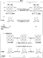
- FIG. 2 is a diagram for explaining the operation (DBC) of the liquid crystal display device 1.
- FIG. 2A shows the gradation of image data before gradation change (before execution of DBC)
- FIG. 2B shows the level of image data after gradation change (after execution of DBC).
- each pixel is composed of three picture elements of R (red), G (Green), and B (blue), and a gradation value is set for each picture element.
- R red
- G Green
- B blue
- a gradation value is set for each picture element.
- the “pixel” shown in FIG. 2A indicates one of R, G, and B picture elements.
- the gradation of the pixel in the target area is 60.
- the pixel value adjustment unit 3312 described later changes the gradation value to 120 at a change magnification of 2 (expansion rate of 2) (a).
- the gradation and the pixel transmittance are proportional.
- the gradation and the BL luminance are changed so that the transmittance ⁇ BL luminance does not change (that is, the pixel luminance does not change).
- FIG. 2 (c) shows the BL brightness before brightness reduction (before DBC execution) (when the brightness is the maximum value is indicated by 100%) and the BL brightness after brightness change (after DBC execution) (50%). ). It is assumed that the BL brightness is the highest value (100%) before the brightness is lowered. At this time, the BL control unit 34, which will be described later, changes the BL brightness to 50% at a reduction factor of 1/2 (reduction rate of 1/2), for example (a).
- (a) gradation change amount and (b) BL luminance change amount are set so as not to change the front luminance (luminance felt by human eyes) of each of a plurality of pixels in the image.
- the front luminance “60” is not changed before and after the DBC.
- the DBC stage control will be described with reference to FIG.
- the initial gradation is set to “60”
- the target gradation is set to “120”.
- the BL brightness is assumed to be set to “100% (maximum brightness)” by default, and the target BL brightness is set to “50%” so as not to change the front brightness “60”. Shall.
- the DBC is preferably controlled step by step using a plurality of frame images. For example, in the example shown in FIG. 2 (e), the gradation of the pixel is increased stepwise from “60” ⁇ “80” ⁇ “120” using three frame images (c), and the BL brightness is increased. Is reduced step by step from “100%” ⁇ “75%” ⁇ “50%” (D).
- the DBC circuit 3 shown in FIG. 1 includes a frame memory 31, an image analysis unit 32, an image processing unit 33, a BL control unit (backlight control unit) 34, and a timer 35 in order to realize the drive function as described above. .
- the image analysis unit 32 of the present embodiment uses the timer 35 to determine whether the image data of the frame image (updated image) whose display is updated in response to the update request is a still image or a moving image. Specifically, the timer 35 is reset at the head of the frame image (updated image) input to the image analysis unit 32. In the case of a moving image, since the frame image is periodically updated, the timer 35 does not exceed a certain time. Within a predetermined period (for example, a period from the start of input of the first image data of a predetermined number of updated images to the end of input of the last image data), the measurement time of the timer 35 is equal to or longer than the above-described fixed time. If it is even once, the image may be determined as a still image. On the other hand, if the measurement time of the timer 35 never exceeds the above-mentioned fixed time within a predetermined period, the image may be determined as a moving image.
- the form for determining whether the image data of the updated image is a still picture or a moving picture is not limited to the above form.
- an update image is often periodically input at a constant cycle such as 30 Hz. Therefore, the time from when the timer 35 is reset to the next reset (or frame image update interval) If the time is within the specified range, it may be determined as a moving image.
- the image analysis unit 32 determines a frequency distribution polygon (histogram) from the distribution of pixel values of each pixel constituting the display panel 42 that displays each image before and after the display update. And calculating a statistical index value based on this, determining whether an index indicating a change before and after the update of the index value is greater than a preset threshold value, and determining the determination result as an image processing unit Control to notify 33 is also performed.
- a frequency distribution polygon Histogram
- the frame memory 31 delays the input of the image data by one frame by temporarily recording and reading the image data. Thereby, the input timing of the image data (before update) and the next input image data (after update) are synchronized. For this reason, the image analysis unit 32 can compare the frame images before and after the update.
- the frame memory 31 is used to delay the image data by one frame.
- the present invention is not limited to this, and a delay circuit that can delay the image data by one frame. If present, the frame memory 31 can be used instead.
- the image processing unit 33 adjusts the refresh rate of the image data displayed on the display unit 4 or changes the pixel value set to each pixel of the display panel 42 that displays an image when performing DBC to a high value.
- the gate voltage is applied to the scanning signal line of the display panel 42 and the data voltage is applied to the data signal line based on the image data of the frame image to be displayed.
- the image processing unit 33 includes a display drive control unit (signal output control unit) 331, a gate driver 332, and a source driver 333.
- the image processing unit 33 includes a refresh control unit 3311, a pixel value adjustment unit 3312, and a TG 3313.
- the display drive control unit 331 is a so-called COG driver mounted on the glass substrate of the display unit 4 (display panel 42), for example, so as to cause the screen to display based on image data. Then, the display unit 4 is driven.
- the display drive control unit 331 instructs the CPU 22 of the host control unit 2 to read out and output the image data of the updated image from the temporary recording unit 23. Do.
- the display drive control unit 331 instructs the CPU 22 of the host control unit 2 as necessary to output at least one DBC that is the same as the updated image after outputting the updated image. Control is performed to read the additional frame image from the temporary recording unit 23 and output it.
- the display drive control unit 331 instructs the CPU 22 of the host control unit 2 according to a refresh rate set by a refresh control unit 3311 to be described later, and displays the image on the update image after outputting the update image. Control is performed so that image data corresponding to the additional refresh image obtained by inverting the polarity of the voltage applied to the electrode of each pixel of the panel 42 is read from the temporary recording unit 23 and output. More specifically, the display drive control unit 331 provides the update image, the additional frame image, and the additional refresh image from the temporary recording unit 23 to the CPU 22 of the host control unit 2 in order to realize the drive control.
- the CPU 22 controls the CPU 22 to output a control signal (image output request; request signal, another request signal) for reading out and outputting image data corresponding to each of the image data.
- the display drive control unit 331 includes a refresh control unit 3311, a pixel value adjustment unit 3312, and a TG 3313 (timing generator) in order to realize the above drive function.
- the refresh control unit 3311 controls the output timing of the additional refresh image by setting the refresh rate of the image displayed on the display panel 42.
- the additional refresh image is image data output after the output of the updated image, and is image data obtained by inverting the polarity of the voltage applied to the electrode of each pixel of the display panel 42 that displays the image.
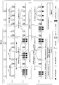
- 5A and 5B show an outline of the output timing of each image data of the update image and the additional refresh image.
- image data of an updated image is output at the output timing shown in FIG.
- the images indicated by “A” to “D” are driven by low refresh
- the images indicated by “E” and “F” are driven by high refresh.
- the time from when the updated image “A” is output to when the additional refresh image “A” is output is 1 second (sec), and an example in which a low refresh rate of 1 Hz is set is shown. ing.
- the time from the output of the updated image “E” to the output of the additional refresh image “E” is 1/60 seconds (sec), and shows an example in which a high refresh rate of 60 Hz is set. ing.
- the refresh rate is set to 24 Hz, 30 Hz, 60 Hz, etc., for example.
- the refresh rate is set to a refresh rate (for example, 1 Hz) lower than the above-mentioned 24 Hz, 30 Hz, 60 Hz, or the like.
- the refresh control unit 3311 notifies the TG 3313 of the refresh rate setting information so that the display panel 42 is driven at the set refresh rate.
- the pixel value adjustment unit 3312 performs control to change the pixel value of each pixel of the display panel 42 (display screen) for displaying an image higher than that before the determination when performing DBC.
- the pixel value adjusting unit 3312 notifies the TG 3313 of pixel value setting information (pixel value change information) of each pixel of the display panel 42 so that the display panel 42 is driven with the pixel value of each set pixel.
- the TG 3313 outputs image data to the source driver 333 based on the refresh rate notified from the refresh control unit 3311 and the pixel value of each pixel notified from the pixel value adjustment unit 3312. Further, the TG 3313 generates a timing signal for driving the display panel 42 at the refresh rate notified from the refresh control unit 3311 and supplies the timing signal to the source driver 333.
- the TG 3313 may use a synchronization signal output from the TG 24 of the host control unit 2 in order to generate a timing signal.
- the source driver 333 stores and outputs the image data input from the TG 3313 for one line at the timing generated by the shift register. Further, the source driver 333 selects a gradation voltage corresponding to the gradation represented by the image data output from the shift register, and outputs it as a data voltage to each source line described later in the display panel 42.
- the gate driver 332 generates a gate signal to be output to each gate line in the display panel 42.
- the gate driver 332 outputs the gate signal to select the gate lines line-sequentially.
- the BL control unit 34 sets the BL luminance of the backlight 41 in advance. Decrease by a predetermined amount from the set value. On the other hand, if the brightness control information has not been received, the BL brightness of the backlight 41 is set to the preset value (usually the maximum brightness).
- the display unit 4 includes a display panel 42 and a backlight 41.
- the display panel 42 is, for example, an oxide semiconductor liquid crystal display panel as an active matrix type liquid crystal display panel.
- An oxide semiconductor liquid crystal display panel is a liquid crystal display panel in which an oxide semiconductor-TFT is employed as a switching element provided corresponding to at least one of a plurality of pixels arranged two-dimensionally.
- An oxide semiconductor-TFT is a TFT in which an oxide semiconductor is used for a semiconductor layer.
- an oxide semiconductor for example, an oxide semiconductor (In—Ga—Zn—O) using an oxide of indium, gallium, and zinc is given.
- An oxide semiconductor-TFT has a large current flowing in an on state and a small leak current in an off state.
- the pixel aperture ratio can be improved and the refresh rate of the screen display can be reduced to about 1 Hz.
- the reduction of the refresh rate brings about a power saving effect.
- the improvement in the pixel aperture ratio brings about an effect of making the display brighter or a power saving effect by reducing the light amount of the backlight 41 when the display brightness is the same as that of the CG silicon liquid crystal display panel or the like.
- the backlight 41 includes a plurality of LEDs (Light Emitting Diodes), and each LED emits light by current supplied from the BL control unit 34. The backlight light emitted from the backlight 41 is applied to the display panel 42.
- the DBC circuit 3 described above may be formed as a dedicated driver LSI, but may be formed on the active matrix substrate (glass substrate) described later of the display unit 4 in a COG configuration.
- Embodiment 1 Operation of Liquid Crystal Display Device 1 (Part 1)
- Part 1 an example of the operation of the liquid crystal display device 1 according to an embodiment of the present invention will be described with reference to FIG.
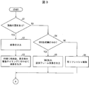
- FIG. 3 is a flowchart for explaining the operation of the liquid crystal display device 1.
- step S (hereinafter, “step” is omitted) 1, for example, as in the above-described example, an application that is started up and being executed in the liquid crystal display device 1 requests (notifies) the image generation unit 21 to update the display. If there is a new image (updated image) that is desired to be displayed, the process proceeds to S2. On the other hand, if there is no updated image, the process proceeds to S4.
- the image generation unit 21 In S2, the image generation unit 21 generates an updated image and proceeds to S3. At this time, the image generation unit 21 notifies the screen update detection unit 25 of a notification that an update image has been generated (update notification). When receiving an update notification from the image generation unit 21, the screen update detection unit 25 determines that the image has been updated, and notifies the DBC circuit 3 and the CPU 22 to that effect (update notification).
- the CPU 22 performs control to temporarily store the updated image generated by the image generation unit 21 in the temporary recording unit 23 (VRAM). Thereafter, when the CPU 22 receives an “image output request (request signal)” relating to the updated image from the display drive control unit 331 of the DBC circuit 3, the CPU 22 sends the image data to the DBC circuit 3 in accordance with the liquid crystal drive timing. Control to output (proceed to “A”).
- the display drive control unit 331 performs low refresh drive (proceeds to “A”). Specifically, the refresh control unit 3311 changes the refresh rate to a predetermined rate as a low refresh rate. In addition, the display drive control unit 331 is currently recorded in the temporary recording unit 23 in order to generate image data of an additional image for refreshing (hereinafter referred to as an additional refresh image) after the update image is output from the TG 24. An “image output request (another request signal)” for outputting image data of the same image as the updated image is transmitted. When the display drive control unit 331 receives the image data from the TG 24, the display drive control unit 331 controls the TG 3313 to output an additional refresh image (proceeds to "A").
- the display drive control unit 331 controls the TG 24 and TG 3313, and after a certain period of time, for example, in order to protect the display panel 42, the temporary recording unit 23 in a cycle of 1 second, for example.
- the image data stored in is output.
- FIG. 4 is a flowchart for explaining the operation of the liquid crystal display device 1.
- FIG. 5 is a timing chart for explaining the operation of the liquid crystal display device 1.
- the image analysis unit 32 determines whether the image data of the updated image input to the DBC circuit 3 is a moving image or a still image using the timer 35 as described above (proceeds to S8). The determination method at this time is as described above.
- the process proceeds to S9. On the other hand, if the image analysis unit 32 determines that the image data of the updated image is a moving image, the process proceeds to S13.
- the image analysis unit 32 indicates the change in the distribution of the pixel values of the display panel 42 that displays the image after the display update with respect to the distribution of the pixel values of the display panel 42 that displays the image before the display update. It is determined whether or not is larger than a threshold value. The determination method at this time is as described above.
- the process proceeds to S11.
- DBC is executed in accordance with the updated image / additional frame image.
- the display drive control unit 331 determines a predetermined number of DBC stage controls, a change range of pixel value increase at each stage, an output image, and an output interval between single or plural additional frame images.
- an “image output request (request signal, another request signal)” is transmitted to the CPU 22 at an appropriate timing.
- the number of times of DBC stage control may be one or more, but it is set to a number that does not cause display flickering and does not greatly deteriorate the power consumption reduction effect of the oxide semiconductor liquid crystal panel. .
- the change width of the pixel value increase in each stage may be determined in advance based on the number of DBC stage control, the initial display screen gradation, the target display screen gradation, and the like.
- the output interval between the updated image and the additional frame image may be set appropriately within a range of 1 second, but it is only enough to prevent display flickering and reduces the power consumption of the oxide semiconductor liquid crystal panel. Do not make it worse.
- the pixel value adjustment unit 3312 performs control to change the pixel value of each pixel of the display panel 42 that displays an image at a predetermined change width higher than that before the determination in each stage of DBC. In addition, when the pixel value adjustment unit 3312 performs control to change the pixel value of each pixel of the display panel 42 higher than that before the determination, the pixel value adjustment unit 3312 notifies the BL control unit 34 of pixel value change information related to the control. . At this time, the BL control unit 34 performs control to lower the luminance of the backlight 41 from that before the determination in accordance with the change of the pixel value of each pixel of the image by the pixel value adjustment unit 3312.
- FIG. 5 shows how an additional frame image for DBC is output when the refresh drive as shown in (b) in FIG. 5 is performed.
- the change in the pixel value distribution of each pixel of the display panel 42 is large
- “ ⁇ ” and “B” in the example after the output of each updated image “ ⁇ ”And“ ⁇ ”
- three additional frame images are output.
- two additional frame images of “ ⁇ ” are output.
- the DBC stage control may be performed on both the updated image and the additional frame image.
- the DBC step control may be performed only on the additional frame image for DBC.
- the number of additional frame images is one less than the three shown in FIG. That is, in FIG. 5D, the output process of the additional frame image “ ⁇ ” is finished earlier than the example shown in FIG.
- the number of additional frame images “ ⁇ ” is small, generation of unnecessary additional frame images can be suppressed as compared with the example shown in (c) of FIG.
- DBC is not executed or DBC is executed in accordance with low refresh driving. More specifically, when the image analysis unit 32 determines that the change in the distribution of pixel values is small or no change, the display drive control unit 331 receives the determination result, and adds an additional frame for DBC. The transmission of the “image output request (request signal, another request signal)” requesting image output is stopped. In this case, as shown in FIG. 5C, the output of the additional frame image is blocked. Alternatively, when the image analysis unit 32 determines that the change in the distribution of pixel values is small or no change, the display drive control unit 331 displays the updated image “B” as illustrated in FIG. ”And the additional refresh image“ B ”, or DBC may be performed on one of the update image“ B ”and the additional refresh image“ B ”.
- the display drive control unit 331 performs the update as in the case where it is determined to be a moving image in the example illustrated in FIG. DBC is performed in accordance with the output of the image data of the image.
- the control blocks (particularly the image analysis unit 32, the image processing unit 33, the BL control unit 34, and the display drive control unit 331) of the DBC circuit 3 are realized by a logic circuit (hardware) formed in an integrated circuit (IC chip) or the like. Alternatively, it may be realized by software using a CPU (Central Processing Unit).
- a logic circuit hardware
- IC chip integrated circuit
- CPU Central Processing Unit
- the DBC circuit 3 records a CPU that executes instructions of a program (dynamic backlight control program) that is software that realizes each function, and the program and various data are readable by a computer (or CPU).
- ROM Read Only Memory
- RAM Random Access Memory
- the objective of this invention is achieved when a computer (or CPU) reads the said program from the said recording medium and runs it.
- a “non-temporary tangible medium” such as a tape, a disk, a card, a semiconductor memory, a programmable logic circuit, or the like can be used.
- the program may be supplied to the computer via an arbitrary transmission medium (such as a communication network or a broadcast wave) that can transmit the program.
- a transmission medium such as a communication network or a broadcast wave
- the present invention can also be realized in the form of a data signal embedded in a carrier wave in which the program is embodied by electronic transmission.
- the control device is a control device (DBC circuit 3) of a display device (liquid crystal display device 1) capable of low refresh rate driving, and is updated in response to a request for updating the display screen display.
- the image analysis unit (32) for determining whether the image is a still image or a moving image; and if it is determined that the image is a moving image, the pixel value of each pixel of the display screen for displaying the image is An image processing unit (33) that performs control to change higher than before the determination, and a backlight control that performs control to lower the luminance of the backlight more than before the determination in accordance with the change of the pixel value of each pixel of the image.
- Unit BL control unit 34).
- DBC DBC is as described above.
- DBC stage control can be performed.
- unnecessary generation of an additional frame image for DBC can be suppressed by performing step control in accordance with a plurality of update images generated periodically. As described above, it is possible to suppress the deterioration of the power consumption reduction effect when DBC processing is enabled for a display device capable of low refresh rate driving.
- the image analysis unit is configured to update the display after updating the display with respect to a distribution of pixel values of the display screen that displays the image before the display is updated. It is determined whether or not an index indicating a change in the distribution of pixel values on the display screen for displaying an image is greater than a threshold, and the image processing unit updates the display when the index is greater than the threshold. Control the pixel value of each pixel of the display screen that displays the image of the display screen to be higher than that before the determination, and the backlight control unit, when the index is greater than the threshold value, In accordance with the change of the pixel value of the pixel, the backlight brightness may be controlled to be lower than that before the determination.
- the image analysis unit indicates the change in the distribution of the pixel values of the display screen that displays the image after the display update with respect to the distribution of the pixel values of the display screen that displays the image before the display update.
- DBC is performed when the index is greater than the threshold.
- the index indicating the change in the distribution of pixel values is larger than the threshold value, there may be a case where the change in the distribution of pixel values is large although it is a still image, in addition to the case where the above-described image is a moving image.
- the increase in the number leads to deterioration of the power consumption reduction effect of the display device that can be driven at a low refresh rate. For this reason, it is necessary to suppress the generation of an additional frame image for DBC as much as possible. Therefore, in the above configuration, assuming that the image is a still image, DBC is performed only when the index indicating the change in the distribution of pixel values is larger than the threshold value. Therefore, when the index indicating the change in the distribution of pixel values is equal to or less than the threshold value, it is not necessary to output an additional frame image. Therefore, the power consumption when DBC processing is enabled for a display device that can be driven at a low refresh rate. The deterioration of the reduction effect can be suppressed.
- the image analysis unit updates the display with respect to a distribution of pixel values of the display screen that displays the image before the display is updated. It is determined whether or not an index indicating a change in the distribution of pixel values on the display screen for displaying a subsequent image is greater than a threshold value. If the index is greater than the threshold value, output of the image after updating the display is performed.
- a signal output control unit (display drive control unit 331) that performs control to output a request signal for reading out and outputting at least one additional frame image that is the same as the image after update of the display from the recording unit,
- the image processing unit is configured to change the pixel value of each pixel of the display screen that displays the at least one additional frame image to be higher than that before the determination. It may be carried out.
- an additional frame image (for DBC) is output only when the index indicating the change in the distribution of pixel values is larger than the threshold value. ing. Therefore, useless output of the additional frame image is suppressed, so that it is possible to suppress the deterioration of the power consumption reduction effect when DBC processing is enabled for a display device capable of low refresh rate driving.
- the signal output control unit may stop outputting the request signal when the index is equal to or less than the threshold value.
- the control device is the control apparatus according to aspect 3 or 4, wherein the signal output control unit is configured to display an image updated in response to a request to update display on the display screen. Performs control to output another request signal for outputting an additional refresh image in which the polarity of the voltage applied to the electrode of each pixel is inverted, and the image processing unit, when the index is equal to or less than the threshold value, You may perform control which changes the pixel value of each pixel of the said display screen which displays an additional refresh image highly.
- the case where the index indicating the change in the distribution of pixel values is equal to or less than the threshold value may be a still image and the change in the distribution of pixel values is small, or there may be no change in the distribution of pixel values.
- DBC is performed for the additional refresh image. That is, by performing DBC on the additional refresh image in addition to the update image, DBC stage control can be performed. As a result, generation of additional frame images for DBC is suppressed, and generation of unnecessary frame images can be suppressed by the amount of additional frame images. As described above, it is possible to suppress the deterioration of the power consumption reduction effect when DBC processing is enabled for a display device capable of low refresh rate driving.
- control device may be realized by a computer, and a dynamic back for causing the computer to execute the processing in the control device according to any one of the above.
- a dynamic backlight control program for causing a computer to execute processing that is lower than before determination, and a computer that records the dynamic backlight control program Recording medium that can be taken only also included in the scope of the present invention.
- the present invention can be used for a display device and a control device for the display device.
- a liquid crystal display device a host controller of the liquid crystal display device, a liquid crystal driver, a liquid crystal driver controller (LCDC), and the like.
- LCDC liquid crystal driver controller
- Display unit (display device) 23 Temporary recording unit (VRAM; recording unit) 32 Image analysis unit 33 Image processing unit 34 BL control unit (backlight control unit) 41 Backlight 331 Display drive control unit (signal output control unit)
Landscapes
- Engineering & Computer Science (AREA)
- Physics & Mathematics (AREA)
- Computer Hardware Design (AREA)
- General Physics & Mathematics (AREA)
- Theoretical Computer Science (AREA)
- Chemical & Material Sciences (AREA)
- Crystallography & Structural Chemistry (AREA)
- Control Of Indicators Other Than Cathode Ray Tubes (AREA)
- Liquid Crystal Display Device Control (AREA)
- Liquid Crystal (AREA)
Abstract
Description
図1は、本実施形態に係る液晶表示装置1の構成を示すブロック図である。同図に示すように、液晶表示装置1は、ホスト制御部2と、DBC回路(制御装置)3と、表示部(表示装置)4と、を備える。
ホスト制御部2は、アプリケーションによる更新要求または外部からの更新要求に応じて更新される1画面分(1フレーム分)のフレーム画像(以下、単に「更新画像」と略称する)の画像データを生成するとともに、生成した画像データを一旦蓄えておき、必要に応じてDBC回路3に転送する。このため、ホスト制御部2は、画像生成部21、CPU22、一時記記録部(記録部)23、TG24(タイミングジェネレータ)、および画面更新検知部25を備えている。ホスト制御部2は、例えば基板上に形成された制御回路で構成される。
DBC回路3は、ホスト制御部2から転送された画像データを表示部4に表示させるように表示部4を駆動するとともに、バックライト41の輝度を制御する制御装置である。このDBC回路3は、動画を表示するときに、24Hz、30Hzおよび60Hzなど、表示部4について予め規定されているリフレッシュレートでリフレッシュ表示を行うように表示部4を駆動する。また、DBC回路3は、入力される画像データの更新の有無に応じてリフレッシュレート(駆動周期)を設定し、設定したリフレッシュレートに基づいて駆動タイミングを生成し、その駆動タイミングに基づいて表示部4を駆動する。また、DBC回路3は、DBC処理を実行中か否かによってDBC用の追加フレーム画像を出力するか否かを決定したり、低リフレッシュ駆動を行うか否かを決定したりする制御も行う。加えて、DBC回路3は、画像が静止画および動画のいずれであるか、または、更新後の画像を表示する表示画面の各画素の画素値(階調値)の分布が、更新前の画素値の分布から大きく変化したか否かによってDBC用の追加フレーム画像を出力するか否かを決定したり、DBCを実行するか否かを決定したり、低リフレッシュ駆動に合せてDBCを実行するか否かを決定したりする制御も行う。
次に、図3に基づき、本発明の一実施形態に係る液晶表示装置1の動作の一例について説明する。図3は、液晶表示装置1の動作を説明するためのフローチャートである。
次に、図4および図5に基づき、本発明の一実施形態に係る液晶表示装置1の動作の別の例について説明する。図4は、液晶表示装置1の動作を説明するためのフローチャートである。また、図5は、液晶表示装置1の動作を説明するためのタイミングチャートである。
DBC回路3の制御ブロック(特に画像解析部32、画像処理部33、BL制御部34および表示駆動制御部331)は、集積回路(ICチップ)等に形成された論理回路(ハードウェア)によって実現してもよいし、CPU(Central Processing Unit)を用いてソフトウェアによって実現してもよい。
本発明の態様1に係る制御装置は、低リフレッシュレート駆動が可能な表示装置(液晶表示装置1)の制御装置(DBC回路3)であって、表示画面の表示の更新の要求に応じて更新された画像が、静止画か動画かを判定する画像解析部(32)と、上記画像が動画であると判定された場合、上記画像を表示する上記表示画面の各画素の画素値を上記の判定前よりも高く変更する制御を行う画像処理部(33)と、上記画像の各画素の画素値の変更に合わせてバックライトの輝度を上記の判定前よりも低下させる制御を行うバックライト制御部(BL制御部34)と、を備えている構成である。
4 表示部(表示装置)
23 一時記録部(VRAM;記録部)
32 画像解析部
33 画像処理部
34 BL制御部(バックライト制御部)
41 バックライト
331 表示駆動制御部(信号出力制御部)
Claims (7)
- 低リフレッシュレート駆動が可能な表示装置の制御装置であって、
表示画面の表示の更新の要求に応じて更新された画像が、静止画か動画かを判定する画像解析部と、
上記画像が動画であると判定された場合、上記画像を表示する上記表示画面の各画素の画素値を上記の判定前よりも高く変更する制御を行う画像処理部と、
上記画像の各画素の画素値の変更に合わせてバックライトの輝度を上記の判定前よりも低下させる制御を行うバックライト制御部と、を備えていることを特徴とする制御装置。 - 上記画像解析部は、上記表示の更新前の画像を表示する上記表示画面の画素値の分布に対する、上記表示の更新後の画像を表示する上記表示画面の画素値の分布の変化を示す指標が閾値よりも大きいか否かを判定し、
上記画像処理部は、上記指標が上記閾値よりも大きい場合、上記表示の更新後の画像を表示する上記表示画面の各画素の画素値を上記の判定前よりも高く変更する制御を行い、
上記バックライト制御部は、上記指標が上記閾値よりも大きい場合、上記表示画面の各画素の画素値の変更に合わせてバックライトの輝度を上記の判定前よりも低下させる制御を行うことを特徴とする請求項1に記載の制御装置。 - 上記画像解析部は、上記表示の更新前の画像を表示する上記表示画面の画素値の分布に対する、上記表示の更新後の画像を表示する上記表示画面の画素値の分布の変化を示す指標が閾値よりも大きいか否かを判定し、
上記指標が上記閾値よりも大きい場合、上記表示の更新後の画像の出力後に、該表示の更新後の画像と同一の少なくとも一つの追加フレーム画像を記録部から読み出して出力させるための要求信号を出力する制御を行う信号出力制御部を備え、
上記画像処理部は、上記指標が上記閾値よりも大きい場合、上記少なくとも一つの追加フレーム画像を表示する上記表示画面の各画素の画素値を上記の判定前よりも高く変更する制御を行うことを特徴とする請求項1または2に記載の制御装置。 - 上記信号出力制御部は、上記指標が上記閾値以下の場合、上記要求信号の出力を停止することを特徴とする請求項3に記載の制御装置。
- 上記信号出力制御部は、上記表示画面の表示の更新の要求に応じて更新された画像を表示する上記表示画面の各画素の電極に印加される電圧の極性を反転させた追加リフレッシュ画像を出力させるための別の要求信号を出力する制御を行い、
上記画像処理部は、上記指標が上記閾値以下の場合、上記追加リフレッシュ画像を表示する上記表示画面の各画素の画素値を高く変更する制御を行うことを特徴とする請求項3または4に記載の制御装置。 - 請求項1から5までのいずれか1項に記載の制御装置における処理をコンピュータに実行させるための動的バックライト制御プログラムであって、
表示画面の表示の更新の要求に応じて更新された画像が、静止画か動画かを判定する処理と、
上記画像が動画であると判定された場合、上記画像を表示する上記表示画面の各画素の画素値を上記の判定前よりも高く変更する処理と、
上記画像を表示する上記表示画面の各画素の画素値の変更に合わせてバックライトの輝度を上記の判定前よりも低下させる処理と、をコンピュータに実行させるための動的バックライト制御プログラム。 - 低リフレッシュレート駆動が可能な表示装置の制御装置の制御方法であって、
表示画面の表示の更新の要求に応じて更新された画像が、静止画か動画かを判定するステップと、
上記画像が動画であると判定された場合、上記画像を表示する上記表示画面の各画素の画素値を上記の判定前よりも高く変更するステップと、
上記画像を表示する上記表示画面の各画素の画素値の変更に合わせてバックライトの輝度を上記の判定前よりも低下させるステップと、を含むことを特徴とする制御方法。
Priority Applications (3)
| Application Number | Priority Date | Filing Date | Title |
|---|---|---|---|
| CN201480048961.8A CN105556587B (zh) | 2013-09-20 | 2014-08-26 | 控制装置和控制装置的控制方法 |
| JP2015537619A JP6140294B2 (ja) | 2013-09-20 | 2014-08-26 | 制御装置、動的バックライト制御プログラムおよび制御装置の制御方法 |
| US14/914,725 US10013922B2 (en) | 2013-09-20 | 2014-08-26 | Control device and control device controlling method |
Applications Claiming Priority (2)
| Application Number | Priority Date | Filing Date | Title |
|---|---|---|---|
| JP2013-196036 | 2013-09-20 | ||
| JP2013196036 | 2013-09-20 |
Publications (1)
| Publication Number | Publication Date |
|---|---|
| WO2015041012A1 true WO2015041012A1 (ja) | 2015-03-26 |
Family
ID=52688667
Family Applications (1)
| Application Number | Title | Priority Date | Filing Date |
|---|---|---|---|
| PCT/JP2014/072306 Ceased WO2015041012A1 (ja) | 2013-09-20 | 2014-08-26 | 制御装置、動的バックライト制御プログラムおよび制御装置の制御方法 |
Country Status (4)
| Country | Link |
|---|---|
| US (1) | US10013922B2 (ja) |
| JP (1) | JP6140294B2 (ja) |
| CN (1) | CN105556587B (ja) |
| WO (1) | WO2015041012A1 (ja) |
Cited By (7)
| Publication number | Priority date | Publication date | Assignee | Title |
|---|---|---|---|---|
| CN105225634A (zh) * | 2015-10-12 | 2016-01-06 | 深圳市华星光电技术有限公司 | Amoled显示器的驱动系统及驱动方法 |
| CN106060438A (zh) * | 2016-07-15 | 2016-10-26 | 乐视控股(北京)有限公司 | 电子设备屏幕背光控制系统及方法 |
| JP2017151369A (ja) * | 2016-02-26 | 2017-08-31 | 株式会社デジタル | 表示制御装置および表示システム |
| WO2017177536A1 (zh) * | 2016-04-12 | 2017-10-19 | 武汉华星光电技术有限公司 | 降低液晶显示模组功耗的控制方法 |
| JP2018532130A (ja) * | 2016-07-29 | 2018-11-01 | ベイジン シャオミ モバイル ソフトウェア カンパニーリミテッド | リフレッシュレートの調整方法及び装置 |
| US10705377B2 (en) | 2018-06-29 | 2020-07-07 | Sharp Kabushiki Kaisha | Liquid crystal display device and method of controlling the same |
| JP2021056447A (ja) * | 2019-10-01 | 2021-04-08 | シャープ株式会社 | 表示制御装置、表示装置、表示制御装置の制御プログラムおよび制御方法 |
Families Citing this family (9)
| Publication number | Priority date | Publication date | Assignee | Title |
|---|---|---|---|---|
| US9805662B2 (en) * | 2015-03-23 | 2017-10-31 | Intel Corporation | Content adaptive backlight power saving technology |
| US10235076B2 (en) * | 2015-12-16 | 2019-03-19 | Accenture Global Solutions Limited | Data pipeline architecture for cloud processing of structured and unstructured data |
| CN108281125B (zh) * | 2018-01-05 | 2021-04-20 | 华为技术有限公司 | 根据人眼特性进行背光亮度调节的方法、装置和设备 |
| US10416808B2 (en) * | 2018-01-17 | 2019-09-17 | Qualcomm Incorporated | Input event based dynamic panel mode switch |
| CN108538260B (zh) * | 2018-07-20 | 2020-06-02 | 京东方科技集团股份有限公司 | 图像显示处理方法及装置、显示装置及存储介质 |
| CN110164356A (zh) * | 2019-06-11 | 2019-08-23 | 惠科股份有限公司 | 数据显示的控制电路及补偿方法 |
| KR20240015988A (ko) * | 2022-07-28 | 2024-02-06 | 엘지디스플레이 주식회사 | 표시 장치 |
| US12087254B2 (en) * | 2022-09-07 | 2024-09-10 | Lenovo (Singapore) Pte. Ltd. | Computing devices, computer-readable medium, and methods for reducing power consumption during video rendering |
| CN116844477A (zh) * | 2023-07-26 | 2023-10-03 | 合肥京东方卓印科技有限公司 | 一种显示设备、静态画面检测方法、装置及介质 |
Citations (4)
| Publication number | Priority date | Publication date | Assignee | Title |
|---|---|---|---|---|
| JP2002156950A (ja) * | 2000-09-08 | 2002-05-31 | Hitachi Ltd | 液晶表示装置 |
| JP2002323876A (ja) * | 2001-04-24 | 2002-11-08 | Nec Corp | 液晶表示装置における画像表示方法及び液晶表示装置 |
| JP2009271349A (ja) * | 2008-05-08 | 2009-11-19 | Sony Corp | 表示制御装置および方法、並びにプログラム |
| WO2013021846A1 (ja) * | 2011-08-05 | 2013-02-14 | シャープ株式会社 | 表示装置およびその制御方法 |
Family Cites Families (9)
| Publication number | Priority date | Publication date | Assignee | Title |
|---|---|---|---|---|
| KR100818013B1 (ko) * | 2004-02-19 | 2008-03-31 | 샤프 가부시키가이샤 | 영상 표시 장치 및 영상 표시 방법 |
| JP4527512B2 (ja) * | 2004-12-08 | 2010-08-18 | Nec液晶テクノロジー株式会社 | 液晶表示装置 |
| JP4566176B2 (ja) | 2006-09-29 | 2010-10-20 | ルネサスエレクトロニクス株式会社 | 表示駆動回路 |
| KR101470636B1 (ko) * | 2008-06-09 | 2014-12-09 | 엘지디스플레이 주식회사 | 액정표시장치 |
| TWI414859B (zh) * | 2009-05-27 | 2013-11-11 | Mstar Semiconductor Inc | 應用於顯示器之控制裝置及控制方法 |
| KR101577233B1 (ko) * | 2009-10-20 | 2015-12-15 | 엘지디스플레이 주식회사 | 액정 표시장치의 구동장치와 그 구동방법 |
| US8866837B2 (en) * | 2010-02-02 | 2014-10-21 | Microsoft Corporation | Enhancement of images for display on liquid crystal displays |
| KR101695290B1 (ko) * | 2010-07-01 | 2017-01-16 | 엘지디스플레이 주식회사 | 액정 표시장치의 구동장치와 그 구동방법 |
| US8854344B2 (en) * | 2010-12-13 | 2014-10-07 | Ati Technologies Ulc | Self-refresh panel time synchronization |
-
2014
- 2014-08-26 JP JP2015537619A patent/JP6140294B2/ja not_active Expired - Fee Related
- 2014-08-26 CN CN201480048961.8A patent/CN105556587B/zh not_active Expired - Fee Related
- 2014-08-26 WO PCT/JP2014/072306 patent/WO2015041012A1/ja not_active Ceased
- 2014-08-26 US US14/914,725 patent/US10013922B2/en active Active
Patent Citations (4)
| Publication number | Priority date | Publication date | Assignee | Title |
|---|---|---|---|---|
| JP2002156950A (ja) * | 2000-09-08 | 2002-05-31 | Hitachi Ltd | 液晶表示装置 |
| JP2002323876A (ja) * | 2001-04-24 | 2002-11-08 | Nec Corp | 液晶表示装置における画像表示方法及び液晶表示装置 |
| JP2009271349A (ja) * | 2008-05-08 | 2009-11-19 | Sony Corp | 表示制御装置および方法、並びにプログラム |
| WO2013021846A1 (ja) * | 2011-08-05 | 2013-02-14 | シャープ株式会社 | 表示装置およびその制御方法 |
Cited By (9)
| Publication number | Priority date | Publication date | Assignee | Title |
|---|---|---|---|---|
| CN105225634A (zh) * | 2015-10-12 | 2016-01-06 | 深圳市华星光电技术有限公司 | Amoled显示器的驱动系统及驱动方法 |
| CN105225634B (zh) * | 2015-10-12 | 2017-11-03 | 深圳市华星光电技术有限公司 | Amoled显示器的驱动系统及驱动方法 |
| JP2017151369A (ja) * | 2016-02-26 | 2017-08-31 | 株式会社デジタル | 表示制御装置および表示システム |
| WO2017177536A1 (zh) * | 2016-04-12 | 2017-10-19 | 武汉华星光电技术有限公司 | 降低液晶显示模组功耗的控制方法 |
| CN106060438A (zh) * | 2016-07-15 | 2016-10-26 | 乐视控股(北京)有限公司 | 电子设备屏幕背光控制系统及方法 |
| JP2018532130A (ja) * | 2016-07-29 | 2018-11-01 | ベイジン シャオミ モバイル ソフトウェア カンパニーリミテッド | リフレッシュレートの調整方法及び装置 |
| US10705377B2 (en) | 2018-06-29 | 2020-07-07 | Sharp Kabushiki Kaisha | Liquid crystal display device and method of controlling the same |
| JP2021056447A (ja) * | 2019-10-01 | 2021-04-08 | シャープ株式会社 | 表示制御装置、表示装置、表示制御装置の制御プログラムおよび制御方法 |
| JP7416532B2 (ja) | 2019-10-01 | 2024-01-17 | シャープ株式会社 | 表示制御装置、表示装置、表示制御装置の制御プログラムおよび制御方法 |
Also Published As
| Publication number | Publication date |
|---|---|
| CN105556587B (zh) | 2018-04-03 |
| US20160210908A1 (en) | 2016-07-21 |
| JPWO2015041012A1 (ja) | 2017-03-02 |
| US10013922B2 (en) | 2018-07-03 |
| CN105556587A (zh) | 2016-05-04 |
| JP6140294B2 (ja) | 2017-05-31 |
Similar Documents
| Publication | Publication Date | Title |
|---|---|---|
| JP6140294B2 (ja) | 制御装置、動的バックライト制御プログラムおよび制御装置の制御方法 | |
| JP7386688B2 (ja) | 表示制御装置、表示装置、表示制御装置の制御プログラムおよび制御方法 | |
| JP6407509B2 (ja) | 制御装置および表示装置 | |
| TWI570704B (zh) | 具有可變再新率之低功率顯示裝置 | |
| JP6509908B2 (ja) | 表示装置、表示装置の制御方法、および制御プログラム | |
| CN107615369B (zh) | 控制装置、显示装置、控制方法、及计算机可读取存储介质 | |
| CN114446239B (zh) | 显示控制方法、装置、系统及显示设备 | |
| WO2019201021A1 (zh) | 一种电子设备的显示屏背光亮度控制方法和电子设备 | |
| CN115512662B (zh) | 图像显示方法、ddic芯片、显示屏模组及终端 | |
| JP7433060B2 (ja) | 表示制御装置、表示装置、制御プログラムおよび制御方法 | |
| JP7030162B1 (ja) | 制御装置、自発光素子を備える表示装置、制御方法および制御プログラム | |
| CN105659312B (zh) | 显示装置、电子设备以及显示装置的控制方法 | |
| JP2022172980A (ja) | 表示制御装置、電子機器、制御プログラムおよび表示制御方法 | |
| WO2019239914A1 (ja) | 制御装置、表示装置および制御方法 | |
| WO2016093138A1 (ja) | 制御装置、表示装置、および表示装置の制御方法 | |
| CN101281741B (zh) | 动态画面的显示装置与方法 | |
| JP2019191520A (ja) | 表示制御装置、表示装置及び表示制御方法 | |
| WO2020140801A1 (zh) | 显示控制装置及方法、显示装置 | |
| JP7348340B2 (ja) | 表示装置 | |
| WO2019239903A1 (ja) | 制御装置、表示装置および制御方法 |
Legal Events
| Date | Code | Title | Description |
|---|---|---|---|
| WWE | Wipo information: entry into national phase |
Ref document number: 201480048961.8 Country of ref document: CN |
|
| 121 | Ep: the epo has been informed by wipo that ep was designated in this application |
Ref document number: 14845139 Country of ref document: EP Kind code of ref document: A1 |
|
| ENP | Entry into the national phase |
Ref document number: 2015537619 Country of ref document: JP Kind code of ref document: A |
|
| WWE | Wipo information: entry into national phase |
Ref document number: 14914725 Country of ref document: US |
|
| NENP | Non-entry into the national phase |
Ref country code: DE |
|
| 122 | Ep: pct application non-entry in european phase |
Ref document number: 14845139 Country of ref document: EP Kind code of ref document: A1 |