WO2015040892A1 - 表示装置 - Google Patents
表示装置 Download PDFInfo
- Publication number
- WO2015040892A1 WO2015040892A1 PCT/JP2014/063847 JP2014063847W WO2015040892A1 WO 2015040892 A1 WO2015040892 A1 WO 2015040892A1 JP 2014063847 W JP2014063847 W JP 2014063847W WO 2015040892 A1 WO2015040892 A1 WO 2015040892A1
- Authority
- WO
- WIPO (PCT)
- Prior art keywords
- pixel
- display device
- green
- pixel electrode
- liquid crystal
- Prior art date
- Legal status (The legal status is an assumption and is not a legal conclusion. Google has not performed a legal analysis and makes no representation as to the accuracy of the status listed.)
- Ceased
Links
Images







Classifications
-
- G—PHYSICS
- G09—EDUCATION; CRYPTOGRAPHY; DISPLAY; ADVERTISING; SEALS
- G09G—ARRANGEMENTS OR CIRCUITS FOR CONTROL OF INDICATING DEVICES USING STATIC MEANS TO PRESENT VARIABLE INFORMATION
- G09G3/00—Control arrangements or circuits, of interest only in connection with visual indicators other than cathode-ray tubes
- G09G3/20—Control arrangements or circuits, of interest only in connection with visual indicators other than cathode-ray tubes for presentation of an assembly of a number of characters, e.g. a page, by composing the assembly by combination of individual elements arranged in a matrix no fixed position being assigned to or needed to be assigned to the individual characters or partial characters
- G09G3/34—Control arrangements or circuits, of interest only in connection with visual indicators other than cathode-ray tubes for presentation of an assembly of a number of characters, e.g. a page, by composing the assembly by combination of individual elements arranged in a matrix no fixed position being assigned to or needed to be assigned to the individual characters or partial characters by control of light from an independent source
- G09G3/3406—Control of illumination source
- G09G3/3413—Details of control of colour illumination sources
-
- G—PHYSICS
- G02—OPTICS
- G02F—OPTICAL DEVICES OR ARRANGEMENTS FOR THE CONTROL OF LIGHT BY MODIFICATION OF THE OPTICAL PROPERTIES OF THE MEDIA OF THE ELEMENTS INVOLVED THEREIN; NON-LINEAR OPTICS; FREQUENCY-CHANGING OF LIGHT; OPTICAL LOGIC ELEMENTS; OPTICAL ANALOGUE/DIGITAL CONVERTERS
- G02F1/00—Devices or arrangements for the control of the intensity, colour, phase, polarisation or direction of light arriving from an independent light source, e.g. switching, gating or modulating; Non-linear optics
- G02F1/01—Devices or arrangements for the control of the intensity, colour, phase, polarisation or direction of light arriving from an independent light source, e.g. switching, gating or modulating; Non-linear optics for the control of the intensity, phase, polarisation or colour
- G02F1/13—Devices or arrangements for the control of the intensity, colour, phase, polarisation or direction of light arriving from an independent light source, e.g. switching, gating or modulating; Non-linear optics for the control of the intensity, phase, polarisation or colour based on liquid crystals, e.g. single liquid crystal display cells
- G02F1/133—Constructional arrangements; Operation of liquid crystal cells; Circuit arrangements
- G02F1/136—Liquid crystal cells structurally associated with a semi-conducting layer or substrate, e.g. cells forming part of an integrated circuit
- G02F1/1362—Active matrix addressed cells
-
- G—PHYSICS
- G09—EDUCATION; CRYPTOGRAPHY; DISPLAY; ADVERTISING; SEALS
- G09G—ARRANGEMENTS OR CIRCUITS FOR CONTROL OF INDICATING DEVICES USING STATIC MEANS TO PRESENT VARIABLE INFORMATION
- G09G3/00—Control arrangements or circuits, of interest only in connection with visual indicators other than cathode-ray tubes
- G09G3/20—Control arrangements or circuits, of interest only in connection with visual indicators other than cathode-ray tubes for presentation of an assembly of a number of characters, e.g. a page, by composing the assembly by combination of individual elements arranged in a matrix no fixed position being assigned to or needed to be assigned to the individual characters or partial characters
- G09G3/34—Control arrangements or circuits, of interest only in connection with visual indicators other than cathode-ray tubes for presentation of an assembly of a number of characters, e.g. a page, by composing the assembly by combination of individual elements arranged in a matrix no fixed position being assigned to or needed to be assigned to the individual characters or partial characters by control of light from an independent source
- G09G3/36—Control arrangements or circuits, of interest only in connection with visual indicators other than cathode-ray tubes for presentation of an assembly of a number of characters, e.g. a page, by composing the assembly by combination of individual elements arranged in a matrix no fixed position being assigned to or needed to be assigned to the individual characters or partial characters by control of light from an independent source using liquid crystals
- G09G3/3607—Control arrangements or circuits, of interest only in connection with visual indicators other than cathode-ray tubes for presentation of an assembly of a number of characters, e.g. a page, by composing the assembly by combination of individual elements arranged in a matrix no fixed position being assigned to or needed to be assigned to the individual characters or partial characters by control of light from an independent source using liquid crystals for displaying colours or for displaying grey scales with a specific pixel layout, e.g. using sub-pixels
-
- G—PHYSICS
- G09—EDUCATION; CRYPTOGRAPHY; DISPLAY; ADVERTISING; SEALS
- G09G—ARRANGEMENTS OR CIRCUITS FOR CONTROL OF INDICATING DEVICES USING STATIC MEANS TO PRESENT VARIABLE INFORMATION
- G09G3/00—Control arrangements or circuits, of interest only in connection with visual indicators other than cathode-ray tubes
- G09G3/20—Control arrangements or circuits, of interest only in connection with visual indicators other than cathode-ray tubes for presentation of an assembly of a number of characters, e.g. a page, by composing the assembly by combination of individual elements arranged in a matrix no fixed position being assigned to or needed to be assigned to the individual characters or partial characters
- G09G3/34—Control arrangements or circuits, of interest only in connection with visual indicators other than cathode-ray tubes for presentation of an assembly of a number of characters, e.g. a page, by composing the assembly by combination of individual elements arranged in a matrix no fixed position being assigned to or needed to be assigned to the individual characters or partial characters by control of light from an independent source
- G09G3/36—Control arrangements or circuits, of interest only in connection with visual indicators other than cathode-ray tubes for presentation of an assembly of a number of characters, e.g. a page, by composing the assembly by combination of individual elements arranged in a matrix no fixed position being assigned to or needed to be assigned to the individual characters or partial characters by control of light from an independent source using liquid crystals
- G09G3/3611—Control of matrices with row and column drivers
- G09G3/3614—Control of polarity reversal in general
-
- G—PHYSICS
- G09—EDUCATION; CRYPTOGRAPHY; DISPLAY; ADVERTISING; SEALS
- G09G—ARRANGEMENTS OR CIRCUITS FOR CONTROL OF INDICATING DEVICES USING STATIC MEANS TO PRESENT VARIABLE INFORMATION
- G09G3/00—Control arrangements or circuits, of interest only in connection with visual indicators other than cathode-ray tubes
- G09G3/20—Control arrangements or circuits, of interest only in connection with visual indicators other than cathode-ray tubes for presentation of an assembly of a number of characters, e.g. a page, by composing the assembly by combination of individual elements arranged in a matrix no fixed position being assigned to or needed to be assigned to the individual characters or partial characters
- G09G3/34—Control arrangements or circuits, of interest only in connection with visual indicators other than cathode-ray tubes for presentation of an assembly of a number of characters, e.g. a page, by composing the assembly by combination of individual elements arranged in a matrix no fixed position being assigned to or needed to be assigned to the individual characters or partial characters by control of light from an independent source
- G09G3/36—Control arrangements or circuits, of interest only in connection with visual indicators other than cathode-ray tubes for presentation of an assembly of a number of characters, e.g. a page, by composing the assembly by combination of individual elements arranged in a matrix no fixed position being assigned to or needed to be assigned to the individual characters or partial characters by control of light from an independent source using liquid crystals
- G09G3/3611—Control of matrices with row and column drivers
- G09G3/3648—Control of matrices with row and column drivers using an active matrix
-
- G—PHYSICS
- G02—OPTICS
- G02F—OPTICAL DEVICES OR ARRANGEMENTS FOR THE CONTROL OF LIGHT BY MODIFICATION OF THE OPTICAL PROPERTIES OF THE MEDIA OF THE ELEMENTS INVOLVED THEREIN; NON-LINEAR OPTICS; FREQUENCY-CHANGING OF LIGHT; OPTICAL LOGIC ELEMENTS; OPTICAL ANALOGUE/DIGITAL CONVERTERS
- G02F2201/00—Constructional arrangements not provided for in groups G02F1/00 - G02F7/00
- G02F2201/52—RGB geometrical arrangements
-
- G—PHYSICS
- G09—EDUCATION; CRYPTOGRAPHY; DISPLAY; ADVERTISING; SEALS
- G09G—ARRANGEMENTS OR CIRCUITS FOR CONTROL OF INDICATING DEVICES USING STATIC MEANS TO PRESENT VARIABLE INFORMATION
- G09G2300/00—Aspects of the constitution of display devices
- G09G2300/04—Structural and physical details of display devices
- G09G2300/0421—Structural details of the set of electrodes
- G09G2300/0426—Layout of electrodes and connections
-
- G—PHYSICS
- G09—EDUCATION; CRYPTOGRAPHY; DISPLAY; ADVERTISING; SEALS
- G09G—ARRANGEMENTS OR CIRCUITS FOR CONTROL OF INDICATING DEVICES USING STATIC MEANS TO PRESENT VARIABLE INFORMATION
- G09G2300/00—Aspects of the constitution of display devices
- G09G2300/04—Structural and physical details of display devices
- G09G2300/0439—Pixel structures
- G09G2300/0452—Details of colour pixel setup, e.g. pixel composed of a red, a blue and two green components
-
- G—PHYSICS
- G09—EDUCATION; CRYPTOGRAPHY; DISPLAY; ADVERTISING; SEALS
- G09G—ARRANGEMENTS OR CIRCUITS FOR CONTROL OF INDICATING DEVICES USING STATIC MEANS TO PRESENT VARIABLE INFORMATION
- G09G2320/00—Control of display operating conditions
- G09G2320/06—Adjustment of display parameters
- G09G2320/0666—Adjustment of display parameters for control of colour parameters, e.g. colour temperature
-
- G—PHYSICS
- G09—EDUCATION; CRYPTOGRAPHY; DISPLAY; ADVERTISING; SEALS
- G09G—ARRANGEMENTS OR CIRCUITS FOR CONTROL OF INDICATING DEVICES USING STATIC MEANS TO PRESENT VARIABLE INFORMATION
- G09G2340/00—Aspects of display data processing
- G09G2340/04—Changes in size, position or resolution of an image
- G09G2340/0457—Improvement of perceived resolution by subpixel rendering
-
- G—PHYSICS
- G09—EDUCATION; CRYPTOGRAPHY; DISPLAY; ADVERTISING; SEALS
- G09G—ARRANGEMENTS OR CIRCUITS FOR CONTROL OF INDICATING DEVICES USING STATIC MEANS TO PRESENT VARIABLE INFORMATION
- G09G2354/00—Aspects of interface with display user
Definitions
- the present invention relates to a direct-view display device such as a liquid crystal display, an organic EL display, a plasma display and the like.
- Patent Document 1 two green subpixels are arranged for four subpixels (red subpixels, blue subpixels, and two green subpixels) in two rows and two columns that constitute one pixel of a liquid crystal panel. A configuration that is disposed diagonally opposite is disclosed.
- Japanese Patent Publication Japanese Patent Laid-Open No. 2001-33757 (published on February 9, 2001)”
- the conventional configuration supplies a display signal to each of the four sub-pixels based on one luminance information (luminance information) corresponding to the pixel position, and is driven in comparison with a sense of fineness (number of pixels).
- luminance information luminance information
- number of power signal lines data signal lines and scanning signal lines
- the present invention provides a direct-view display device that can provide a high-definition feeling while suppressing the number of signal lines to be driven (number of input terminals).
- a first pixel of green, a second pixel of blue, a third pixel of green, and a fourth pixel of red are arranged in a Bayer array (for the first to fourth pixels in 2 rows and 2 columns, the first pixel of green Brightness information corresponding to the pixel position of the first pixel, which is a source of the display signal supplied to the first pixel, and a display panel for direct viewing, in which the third pixel is diagonally opposed)
- the luminance information corresponding to the pixel position of the third pixel, which is the source of the display signal supplied to the third pixel, is different.
- the number of signal lines to be driven is smaller than that of fineness (the number of pixels), and a direct-view display device that achieves a high-definition feeling while suppressing the number of input terminals is realized.
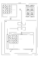
- FIG. 1 is a block diagram illustrating a configuration of a liquid crystal display device of Example 1.
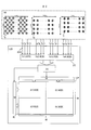
- FIG. 1 is a schematic diagram illustrating a configuration of a liquid crystal display device of Example 1.
- FIG. 10 is a block diagram which shows the effect of Example 1.
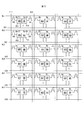
- FIG. 10 is a schematic diagram illustrating a driving method according to the second embodiment.
- FIG. 10 is a schematic diagram illustrating another driving method according to the second embodiment.
- FIG. 10 is a schematic diagram illustrating still another driving method according to the second embodiment.
- FIG. 10 is a schematic diagram illustrating still another driving method according to Embodiment 2.
- 6 is a schematic diagram illustrating a configuration of a liquid crystal display device of Example 2.
- FIG. 10 is a schematic diagram illustrating another configuration of the liquid crystal display device according to the second embodiment.
- FIG. 10 is a schematic diagram showing still another configuration of the liquid crystal display device of Example 2.
- 6 is a schematic diagram illustrating a configuration of a liquid crystal display device of Example 3.
- FIG. 10 is a schematic diagram showing another configuration of the liquid crystal display device of Example 3.
- 6 is a schematic diagram illustrating a configuration of a backlight according to Example 4.
- FIG. FIG. 10 is a schematic diagram illustrating a configuration of a liquid crystal display device of Example 5.
- FIG. 10 is an explanatory diagram illustrating a driving method of the liquid crystal display device of Example 5.
- FIG. 10 is an explanatory diagram for explaining pixel data in Embodiment 5.
- the display device 10 includes an input processing circuit IPC, a display control circuit DCC, a panel drive circuit PDC, and a display panel DP for direct viewing.
- the input processing circuit IPC processes the video signal IGS transmitted from the signal generation device SGD and inputs it to the display control circuit DCC.
- the display control circuit DCC controls the panel drive circuit PDC, and the panel drive circuit PDC drives the display panel DP.
- the green first pixel Gp (1), the blue second pixel Bp (2), the green third pixel Gp (3), and the red fourth pixel Rp (4) are in a Bayer array, that is, For the first to fourth pixels in 2 rows and 2 columns (the horizontal direction in the figure is the row direction and the vertical direction in the figure is the column direction), the green first pixel Gp (1) and the green third pixel Gp ( 3) is diagonally opposed, and the blue second pixel Bp (2) and the red fourth pixel Rp (4) are diagonally opposed.
- This Bayer arrangement is also called a dual green system (DG system).
- the luminance signal Y1 corresponding to the pixel position of the first pixel Gp (1), which is the source of the display signal supplied to the green first pixel Gp (1), and blue
- the luminance signal Y2 corresponding to the pixel position of the second pixel Bp (2), which is the source of the display signal supplied to the second pixel Bp (2), and the green third pixel Gp (3)
- a luminance signal Y3 corresponding to the pixel position of the third pixel Gp (3) and a display signal supplied to the red fourth pixel Rp (4).
- the luminance signal Y4 corresponding to the pixel position of the pixel Rp (4) is separate.
- each pixel column includes a green pixel
- each pixel row includes a green pixel.
- the fineness does not change significantly.
- the number of pixels of the display panel DP is equal to the input terminal necessary for driving the pixels of the display panel DP, and the row direction is larger than that of the sub-pixel type display device as described above.
- the input terminals in the (horizontal direction) can be reduced to 1/3.
- the number of pixels of the display panel DP is, for example, horizontal 8K (about 8000) ⁇ longitudinal 4000 (4K), the number of horizontal input terminals is 8K (in the sub-pixel display device as described above, 24K input terminals in the direction are required), and a direct-view display device that can obtain a high-definition feeling while suppressing the number of input terminals becomes possible.
- the display device 10 include a liquid crystal display device having a direct-view type liquid crystal panel, an organic EL display, a plasma display, and the like, but a display using an IPS liquid crystal or an OLED (organic light emitting diode) as a pixel is more preferable.
- the preferred angle of view is 70 inches diagonal or less, but of course not limited.
- the preferred screen brightness is 150-300 Cd or less. However, in consideration of outdoor use, it is desirable to have a switching mode to ultra-high brightness (for example, 600 Cd or more). Although DG projectors are currently available, focus adjustment is difficult due to their principles, and they cannot be used in bright places. If the screen is not fixed, accurate display is not possible. Can only be used where it can be maintained).
- the liquid crystal display device LCD includes an input processing circuit IPC, a display control circuit DCC, a source driver SD, a gate driver GD, a liquid crystal panel LCP for direct viewing, And a backlight BL.
- the input processing circuit IPC processes the video signal (imaging signal) IGS transmitted from the imaging device CAM, which is a signal generation device, and inputs it to the display control circuit DCC.
- the display control circuit DCC controls the source driver SD and the gate driver GD, and the source driver SD and the gate driver GD drive the liquid crystal panel LCP.
- the arrangement of the photosensors of the image pickup apparatus CAM according to the first embodiment is a Bayer arrangement, that is, first to fourth photosensors (Gs (1) ⁇ Bs (2) ⁇ Gs (3) ⁇ Rs (4) of 2 rows and 2 columns. ),
- the green first photosensor Gs (1) and the green third photosensor Gs (3) are diagonally opposite, the blue second photosensor Bs (2) and the red fourth photosensor Rs (4).
- the green first pixel Gp (1), the blue second pixel Bp (2), the green third pixel Gp (3), and the red fourth pixel Rp (4) are Bayer arranged. It is said.
- the input processing circuit IPC based on the luminance signal Y1 from the green first photosensor Gs (1), the pixel data Gd (1) of the green first pixel Gp (1). And the pixel data Bd (2) of the blue second pixel Bp (2) is generated based on the luminance signal Y2 from the blue second photosensor Gs (2), and the green third photosensor Gs. Based on the luminance signal Y3 from (3), pixel data Gd (3) of the green third pixel Gp (3) is generated, and based on the luminance signal Y4 from the red fourth photosensor Rs (4). Pixel data Rd (4) of the fourth red pixel Rp (4) is generated.
- the video signal IGS from the imaging device CAM is, for example, 8K (about 8000) ⁇ 4K (about 4000) size, green luminance signals Yg (16K) arranged in a checkered pattern, and a matrix
- the number of pixels of the liquid crystal panel LCP is, for example, 8K (about 8000) ⁇ 4K (about 4000), and the input to the input processing circuit IPC is, for example, 16 systems (16 HD- SDI cable: High Definition Serial Digital Interface cable).
- the liquid crystal panel LCP is divided into four regions (A1 to A4 regions and A1 to A4 regions each having a size of 4K ⁇ 2K) vertically and horizontally, and four luminance signals Ya1 corresponding to the region A1 (for Yg) are used.
- the luminance signal Ya2 corresponding to the area A2 is 4 (2 for Yg, 2 for Yg, One Yb and one Yr HD-SDI cable (2K ⁇ 1K per line), and four luminance signals Ya3 corresponding to the area A3 (two for Yg, one for Yb) And one Yr HD-SDI cable (2K ⁇ 1K per line), and four luminance signals Ya4 corresponding to the area A4 (two for Yg, one for Yb, Yr 1) HD-SDI cable (2K x 1K per cable) Is input via.
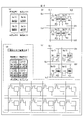
- the pixel electrode PE1 of the green first pixel Gp (1) is connected to the data signal line SL1 and the scanning signal line GL1 through the transistor TR1.
- the pixel electrode PE2 of the blue second pixel Bp (2) is connected to the data signal line SL1 and the scanning signal line GL2 through the transistor TR2, and the pixel electrode PE3 of the green third pixel Gp (3) is connected to the transistor.
- the pixel electrode PE4 of the red fourth pixel Rp (4) is connected to the data signal line SL2 and the scanning signal line GL1 through the transistor TR4, connected to the data signal line SL2 and the scanning signal line GL2 through TR3. Yes.
- the auxiliary capacitance line CS1 forms an auxiliary capacitance with each of the pixel electrode PE1 and the pixel electrode PE4, and the auxiliary capacitance line CS2 forms an auxiliary capacitance with each of the pixel electrode PE2 and the pixel electrode PE3.
- the display signal gd1 corresponding to the pixel data Gd (1) is written to the pixel electrode PE1 via the data signal line SL1 and the transistor TR1, and the pixel electrode PE2 is written via the data signal line SL1 and the transistor TR2.
- the display signal bd2 corresponding to the pixel data Bd (2) is written, and the display signal gd3 corresponding to the pixel data Gd (3) is written to the pixel electrode PE3 via the data signal line SL2 and the transistor TR3.
- a display signal rd4 corresponding to the pixel data Rd (4) is written to the electrode PE4 via the data signal line SL2 and the transistor TR4.
- FIG. 4B is merely an example of the liquid crystal panel LCP, and for example, a configuration as shown in FIG.
- the luminance signal y1 corresponding to the first pixel PiX1 is used to generate three sub-pixels SR, SG, SB sub-pixel data r1, g1, and b1 are generated, and sub-pixel data r2, g2, and b2 of the three sub-pixels SR, SG, and SB are generated from the luminance signal y2 corresponding to the second pixel PiX2, and the third pixel Sub-pixel data r3, g3, and b3 of three subpixels SR, SG, and SB are generated from the luminance signal y3 corresponding to PiX3, and the three subpixels SR, SG, and SB are generated from the luminance signal y4 corresponding to the fourth pixel PiX4.
- the subpixel data r4, g4, and b4 are generated, and the twelve subpixels are driven by six data signal lines and two scanning signal lines). Without degrading the sensitive less, it is possible to reduce the number of data signal lines (the number of source terminal) to 1/3.
- the DG video signal IGS from the imaging device CAM can be directly displayed on the DG liquid crystal panel LCP. Therefore, processing such as resolution conversion (processing that may cause loss of original characteristics) necessary for display on a general sub-pixel type liquid crystal display device can be eliminated or minimized.
- Example 2 In the second embodiment, as shown in FIGS. 5 to 7, the writing polarity of the display signal to the liquid crystal panel LCP is inverted every 2 ⁇ i (i is a natural number) pixels in one pixel row, and 2 in one pixel column.
- Xj (j is a natural number) Invert every pixel. From the viewpoint of the power consumption and the charging rate of the driver, it is desirable to increase i and j. However, when i and j are increased, the display quality may be deteriorated due to visual recognition of flicker or the like.
- SHV Super Hi-Vision
- ITU-BT.2020 SHV (Super Hi-Vision) viewing as defined by ITU-BT.2020
- H is the diagonal length of the display unit.
- the recognition accuracy is based on CRT (interlace drive) 1H (horizontal line) stripe display, and in the second embodiment, the flicker units (positive polarity blocks and negative polarity blocks) are arranged in a checkered pattern.
- the horizontal direction generally has higher recognition accuracy between the resolution in the vertical direction (column direction) and the resolution in the horizontal orientation (row direction).
- the arrangement of the data signal lines to be connected (left side and right side) is changed between one of the two adjacent pixel columns and the other, but the present invention is not limited to this.
- the arrangement of the data signal lines to be connected (left side and right side) can be aligned between one and the other of the two adjacent pixel columns (for example, aligned on the left side as shown in FIG. 8).
- At least one of i and j is set by a setting signal input from the setting unit SS provided in the liquid crystal display device LCD to the display control circuit DCC.
- the setting unit SS generates a setting signal in response to an instruction (user input) from a user input unit integrated with the liquid crystal display device LCD or a user input device separate from the liquid crystal display device LCD.
- the setting unit SS may generate a setting signal according to the distance between the viewer and the screen obtained from the human sensor PS provided in the liquid crystal display device LCD. it can.
- a setting signal is usually generated according to the distance between the viewer and the screen obtained from the human sensor PS (at least one of i and j is automatically set).
- a configuration in which a setting signal is generated according to a user input from the user input device LC (remote controller) may be used.
- Example 3 In Example 3, as shown in FIG. 12, the effective area of the green first pixel Gp (1) is made smaller than the effective area of the blue second pixel Bp (2).
- the effective area of the green third pixel Gp (3) is equal to that of the green first pixel Gp (1), and the effective area of the red fourth pixel Rp (4) is the blue second pixel Bp (2). ) To be equal to the effective area.
- the area of the pixel electrode corresponding to the green first pixel Gp (1) is smaller than the area of the pixel electrode corresponding to the blue second pixel Bp (2), and the green first of the color filter.
- the area of the portion corresponding to the pixel Gp (1) is smaller than the area of the portion corresponding to the blue second pixel Bp (2) of the color filter.
- each color of the entire screen can be reduced without substantially reducing the luminance efficiency of the entire liquid crystal panel as compared with methods such as relatively suppressing the display signal of the green pixels and lowering the green luminance of the backlight BL.
- Brightness balance can be set. Further, an effect of increasing sharpness can be obtained by reducing the area of the green pixel.
- the distance between the barycentric position (white circle) of the first green pixel Gp (1) and the barycentric position (white triangle) of the third green pixel Gp (3) is the second blue pixel Bp (2 ) And the center of gravity (black circle) of the red fourth pixel Rp.
- the green first pixel Gp (1) and the fourth pixel Rp (4) are adjacent to each other in the row direction, and the two data signal lines SL1 and SL2 extending in the column direction are the first to fourth.
- the pixels Gp (1), Bp (2), Gp (3), and Rp (4) are provided so that the first and second pixels Gp (1) and Bp (2) are the same from the data signal line SL1.
- the third and fourth pixels Gp (3) and Rp (4) are separated from each other by the same distance from the data signal line SL2, and the row direction (scanning signal line and (Width in the parallel direction) is smaller than the width in the row direction of the red fourth pixel Rp (4), and the width in the row direction of the green third pixel Gp (3) is that of the blue second pixel Bp (2). It is smaller than the width in the line direction.
- the sharpness is further increased by reducing each of the green first pixel Gp (1) and the green third pixel Gp (3) and separating them.
- the first green pixel Gp (1), the second blue pixel Bp (2), the third green pixel Gp (3), and the fourth red pixel Rp (4 ) The area of each pixel electrode may be made equal, and the light shielding region LB may be formed in a portion corresponding to the green first pixel Gp (1) and the green third pixel Gp (3) of the color filter.
- the pixel electrode of the green first pixel Gp (1) has a substantially rectangular shape, and is obtained by reducing one side or both sides of the pixel electrode of the blue second pixel Bp (2). is there.
- a cut triangle or quadrangle
- an oblique electric field generated around the cut portion changes the liquid crystal alignment, making it difficult to control response. There is a fear.
- the area of the pixel electrode corresponding to green is adjusted so that the pixel electrode corresponding to green is substantially similar to or similar to the pixel electrode corresponding to blue or red (in this case, a rectangle). That is, since the influence of the signal line is linear and easy to correct, the area is adjusted by shortening only one side of the rectangular pixel electrode. Also in this case, in order to minimize the influence on the display, it is desirable to shorten the side parallel to the scanning signal line as shown in FIGS.
- Example 4 the backlight BL can adjust the color balance between green and other colors, and the effective area of the green first pixel Gp (1) and the effective blue second pixel Bp (2).
- the color balance is set according to the ratio of the area or the ratio of the effective area of the green first pixel Gp (1) to the effective area of the red fourth pixel Rp (2). In this way, setting independent of the pixel structure is facilitated.
- the backlight BL is a direct type having a plurality of illumination units LU including a red (R) LED element, a green (G) LED element, and a blue (B) LED element. It is an LED lighting device, and it is desirable that each color LED element can be independently controlled by the lighting control circuit LCC.
- the backlight BL includes an edge-type illumination unit EDLU (LZ) including a green laser generating element, and the green laser light is supplied to the liquid crystal panel LCP via the light guide plate LG. It can also be set as the structure made.
- the green reproduction range defined in the SHV standard ITU BT.2020 is 520 nm-530 nm, and a green laser is optimal for realizing this wavelength band.
- an edge-type illumination unit EDLU (LED) including an LED element as shown in FIG. 14B can be used.
- an edge-type illumination unit including a laser generating element can be used.
- the liquid crystal panel LCP can also be configured as shown in FIG. That is, the green first pixel Gp (1) is connected to the scanning signal line GL1 and the data signal line SL1 via the transistor TR1, and the blue second pixel Bp (2) is connected to the scanning signal line GL1 via the transistor TR2. Connected to the data signal line SL1, the green third pixel Gp (3) is connected to the scanning signal line GL1 and the data signal line SL2 via the transistor TR3, and the red second pixel Rp (4) is connected to the transistor TR4.
- auxiliary capacitance line CS1 forms auxiliary capacitances with the green first pixel Gp (1) and the red fourth pixel Rp (4), respectively.
- CS2 forms an auxiliary capacitance with each of the blue second pixel Bp (2) and the green third pixel Gp (3).
- one auxiliary capacitor line (for example, CS2) is shared by two adjacent pixel rows.
- Example 5 in the field period 1, the luminance of the first pixel Gp (1) is made higher than the luminance of the second pixel Bp (2).
- the luminance of one pixel Gp (1) is made to correspond to the pixel data Gd (1) of the first pixel Gp (1) based on the luminance signal Y1
- the luminance of the third pixel Gp (3) is set to the fourth pixel Rp (4).
- the luminance of the third pixel Gp (3) is made to correspond to the pixel data Gd (3) of the third pixel Gp (3) based on the luminance signal Y3.
- the field period 2 subsequent to the field period 1 as shown in FIGS.
- the luminance of the second pixel Bp (2) is set higher than the luminance of the first pixel Gp (1).
- the luminance of the second pixel Bp (2) is made to correspond to the pixel data Bd (2) of the second pixel Bp (2) based on the luminance signal Y2, and the luminance of the fourth pixel Rp (4) is The luminance of the fourth pixel Rp (4) is made to correspond to the pixel data Rd (4) of the fourth pixel Rp (4) based on the luminance signal Y4 by making it higher than the luminance of the third pixel Gp (3).
- the scanning signal lines GL1, the data signal lines SL1 and SL2, and the auxiliary capacitance lines CS1 and CS2 are driven as shown in FIG. 16, for example. That is, the polarity of each of the data signal lines SL1 and SL2 is inverted every 1H (horizontal scanning period), and the polarity at the start of the field period is inverted every two fields. Further, the polarities of the data signal lines SL1 and SL2 in the same horizontal scanning period are reversed.
- the potentials of the storage capacitor lines CS1 and CS2 are made to have an amplitude (Low to High) at a constant period (eg, nH), and the potential of the storage capacitor line CS1 is set to “Low” during the selection period of the scanning signal line GL1 in the field period 1.
- L the potential of the auxiliary capacitor line CS2 is set to“ High (H) ”
- the potential of the auxiliary capacitor line CS2 is set to“ L ”after the selection period ends.
- the potential of the storage capacitor line CS1 is set to “H”
- the potential of the storage capacitor line CS2 is set to “L”
- the potential of the storage capacitor line CS1 is set to “ L ”(push down)
- the potential of the auxiliary capacitance line CS2 is set to“ H ”(push up).
- the number of data signal lines (the number of input terminals on the source side) and the number of scanning signal lines (the number of input terminals on the gate side) are reduced as compared with the configuration shown in FIG. be able to.
- the pixel data Gd (1) ⁇ Bd (2) ⁇ Gd (3) ⁇ Rd (4) in FIG. 15 is the same frame of the video signal IGS in FIG. It may be obtained from Also, as shown in FIG. 17B, the pixel data Gd (1) and Gd (3) in FIG. 15 are obtained from a certain frame (for example, frame 1: odd frame) of the video signal IGS, The pixel data Bd (2) / Rd (4) may be obtained from another frame (for example, frame 2, even frame) of the video signal IGS.
- the display device includes a direct-view display panel in which a first pixel of green, a second pixel of blue, a third pixel of green, and a fourth pixel of red are arranged in a Bayer array, and is supplied to the first pixel.
- the luminance information corresponding to the pixel position of the first pixel, which is the source of the display signal, and the luminance information corresponding to the pixel position of the third pixel, which is the source of the display signal supplied to the third pixel, are different. It can also be set as the thing which is.
- the display device includes the first to fourth light receiving units described above in an imaging device in which the first green light receiving unit, the second blue light receiving unit, the third green light receiving unit, and the fourth red light receiving unit are arranged in a Bayer array.
- the first to fourth imaging signals obtained from the above can be displayed on the first to fourth pixels.
- the display panel is a liquid crystal panel, and the first pixel and the second or fourth pixel are adjacent to each other in the column direction, and the writing polarity of the data signal is 2 ⁇ i (where i is 1 ⁇ A natural number) may be inverted for each pixel, and may be inverted for each 2 ⁇ j (j is a natural number) pixels in one pixel column.
- the present display device may be configured such that at least one of i and j is variable.
- the display device includes a user input unit integrated with the display device or a setting unit that sets at least one of i and j in response to an instruction from a user input device separate from the display device. You can also
- the present display device may be configured to include a human sensor and a setting unit that sets at least one of i and j according to the distance between the observer obtained from the human sensor and the screen.
- the extension direction of the data signal lines of the liquid crystal panel may be the column direction, and the i may be smaller than the j.
- the present display device may be configured such that the effective area of the first pixel is smaller than the effective area of the second pixel.
- the display panel is a liquid crystal panel, and the area of the first pixel electrode corresponding to the first pixel is equal to the area of the second pixel electrode corresponding to the second pixel, and the first pixel of the color filter. It is also possible to adopt a configuration in which a light shielding region is formed in a portion facing the electrode.
- the display panel is a liquid crystal panel, and an area of the first pixel electrode corresponding to the first pixel is smaller than an area of the second pixel electrode corresponding to the second pixel, and the first color filter includes The area of the portion facing the pixel electrode may be smaller than the area of the portion facing the second pixel electrode of the color filter.
- the first pixel electrode may have a shape obtained by reducing one side or both sides of the second pixel electrode having a substantially rectangular shape.
- the third pixel electrode corresponding to the third pixel has the same shape as the first pixel electrode
- the fourth pixel electrode corresponding to the fourth pixel has the same shape as the second pixel electrode.
- the distance between the barycentric position of the first pixel electrode and the barycentric position of the third pixel electrode is larger than the distance between the barycentric position of the second pixel electrode and the barycentric position of the fourth pixel electrode. You can also.
- the display panel is a liquid crystal panel, and includes a lighting device provided on the back surface of the liquid crystal panel, and the lighting device can adjust the color balance between green and other colors,
- the color balance may be set according to the ratio between the effective area of the first pixel and the effective area of the second pixel, or the ratio between the effective area of the first pixel and the effective area of the fourth pixel.
- the lighting device is a direct type LED lighting device including a red LED element, a green LED element, and a blue LED element, and each LED element of each color can be controlled independently.
- the lighting device may include a green laser generating element, and the green laser light may be supplied to the liquid crystal panel via a light guide plate.
- the first pixel is connected to the first scanning signal line and the first data signal line via the first transistor
- the second pixel is connected to the first scanning signal line and the first data via the second transistor.
- the luminance of the first pixel in the first field period, is higher than the luminance of the second pixel, and in the second field period following the first field period, the luminance of the second pixel is higher than the luminance of the first pixel. It can also be set as a high structure.
- the luminance of the third pixel is higher than the luminance of the fourth pixel in the first field period, and the luminance of the fourth pixel is higher than the luminance of the third pixel in the second field period following the first field period. It can also be set as a high structure.
- the luminance of the first pixel in the first field period corresponds to the input video signal of the first pixel in the first frame
- the luminance of the second pixel in the second field period is the first frame. It is also possible to adopt a configuration corresponding to the video signal of the second pixel.
- the luminance of the first pixel in the first field period corresponds to the input video signal of the first pixel in the first frame
- the luminance of the second pixel in the second field period is the first frame. It is also possible to adopt a configuration corresponding to the video signal of the second pixel of the second frame that is input after.
- the present invention is not limited to the above-described embodiments, and those obtained by appropriately modifying the above-described embodiments based on common general technical knowledge and those obtained by combining them are also included in the embodiments of the present invention.
- the present invention is particularly suitable for a high resolution display.
Landscapes
- Engineering & Computer Science (AREA)
- Physics & Mathematics (AREA)
- General Physics & Mathematics (AREA)
- Theoretical Computer Science (AREA)
- Computer Hardware Design (AREA)
- Chemical & Material Sciences (AREA)
- Crystallography & Structural Chemistry (AREA)
- Nonlinear Science (AREA)
- Optics & Photonics (AREA)
- Mathematical Physics (AREA)
- Microelectronics & Electronic Packaging (AREA)
- Liquid Crystal Display Device Control (AREA)
- Control Of Indicators Other Than Cathode Ray Tubes (AREA)
Abstract
本表示装置は、緑の第1画素、青の第2画素、緑の第3画素、および赤の第4画素がベイヤー配列とされた直視用の表示パネルを備え、第1画素に供給される表示信号のもとになる、第1画素の画素位置に対応する輝度情報と、第3画素に供給される表示信号のもとになる、第3画素の画素位置に対応する輝度情報とが別々のものである。
Description
本発明は、液晶ディスプレイ、有機ELディスプレイ、プラズマディスプレイ等の直視型表示装置に関する。
特許文献1には、液晶パネルの1画素を構成する2行2列の4つのサブ画素(赤のサブ画素、青のサブ画素、2つの緑のサブ画素)について、2つの緑のサブ画素を斜め向かいに配する構成が開示されている。
上記従来の構成は、画素位置に応じた1つの輝度情報(輝度情報)に基づいて上記4つのサブ画素それぞれに表示信号を供給するものであり、精細感(画素数)に比して駆動すべき信号線(データ信号線や走査信号線)の数が多いという問題がある。
本発明では、駆動すべき信号線の数(入力端子数)を抑えながら高精細感が得られる直視型表示装置を提供する。
本表示装置は、緑の第1画素、青の第2画素、緑の第3画素、および赤の第4画素がベイヤー配列(2行2列の第1~第4画素について、緑の第1および第3画素が斜め向かいとなる配列)とされた直視用の表示パネルを備え、第1画素に供給される表示信号のもとになる、第1画素の画素位置に対応する輝度情報と、第3画素に供給される表示信号のもとになる、第3画素の画素位置に対応する輝度情報とが別々のものである。
本発明の一態様では、精細感(画素数)に比して駆動すべき信号線が少なくなり、入力端子数を抑えながら高精細感が得られる直視型表示装置が実現される。
図1に示すように、本実施の形態にかかる表示装置10は、入力処理回路IPCと、表示制御回路DCCと、パネル駆動回路PDCと、直視用の表示パネルDPとを有する。入力処理回路IPCは、信号生成装置SGDから送信された映像信号IGSを処理し、表示制御回路DCCに入力する。表示制御回路DCCはパネル駆動回路PDCを制御し、パネル駆動回路PDCは表示パネルDPを駆動する。
表示パネルDPでは、緑の第1画素Gp(1)、青の第2画素Bp(2)、緑の第3画素Gp(3)、および赤の第4画素Rp(4)がベイヤー配列、すなわち、2行2列(図中横方向を行方向、図中縦方向を列方向とする)の第1~第4画素について、緑の第1画素Gp(1)および緑の第3画素Gp(3)が斜め向かいとなり、青の第2画素Bp(2)および赤の第4画素Rp(4)が斜め向かいとなる配列とされる。このベイヤー配列は、デュアルグリーン方式(DG方式)とも呼ばれる。
ここで、図1に示すように、緑の第1画素Gp(1)に供給される表示信号のもとになる、第1画素Gp(1)の画素位置に対応する輝度信号Y1と、青の第2画素Bp(2)に供給される表示信号のもとになる、第2画素Bp(2)の画素位置に対応する輝度信号Y2と、緑の第3画素Gp(3)に供給される表示信号のもとになる、第3画素Gp(3)の画素位置に対応する輝度信号Y3と、赤の第4画素Rp(4)に供給される表示信号のもとになる、第4画素Rp(4)の画素位置に対応する輝度信号Y4と、が別々のものである。
表示装置10では、緑の画素が市松状に配され、いずれの画素列も緑の画素を含み、いずれの画素行も緑の画素を含むため、同じ画素数のサブ画素方式(例えば、1つの輝度信号Yに対応する1つの画素を、行方向に並ぶR・G・Bの3つのサブ画素に分割し、各サブ画素を駆動する方式)の表示装置と比べて精細感は大きく変わらない。一方で、表示装置10では、表示パネルDPの画素数と、表示パネルDPの画素を駆動するために必要な入力端子とが等しく、上記のようなサブ画素方式の表示装置に比べて、行方向(横方向)の入力端子を1/3に削減することができる。表示パネルDPの画素数を、例えば、横8K(約8000)×縦4000(4K)とすれば、横方向の入力端子は8K個で済み(上記のようなサブ画素方式の表示装置では、横方向の入力端子は24K個必要)、入力端子数を抑えながら高精細感が得られる直視型表示装置が可能となる。なお、表示装置10としては、直視型の液晶パネルを有する液晶表示装置、有機ELディスプレイ、プラズマディスプレイ等が挙げられるが、画素にIPS液晶またはOLED(有機発光ダイオード)を用いたディスプレイがより望ましい。好ましい画角サイズは対角70インチ以下であるが、もちろん限定されない。好ましい画面輝度は、150-300Cd以下である。ただし、屋外使用を考慮して、超高輝度(例えば、600Cd以上)への切り替えモードをもつことが望ましい。なお、DG方式のプロジェクターは現時点で販売されているが、その原理からフォーカス調整が大変であり、明るい場所では使えない、スクリーンが固定されていないと正確な表示ができない(投射室など専用の環境が維持できるところでしか使用できない)などの問題がある。
[実施例1]
図2・3に示すように、実施例1にかかる液晶表示装置LCDは、入力処理回路IPCと、表示制御回路DCCと、ソースドライバSDと、ゲートドライバGDと、直視用の液晶パネルLCPと、バックライトBLとを有する。入力処理回路IPCは、信号生成装置である撮像装置CAMから送信された映像信号(撮像信号)IGSを処理し、表示制御回路DCCに入力する。表示制御回路DCCは、ソースドライバSDおよびゲートドライバGDを制御し、ソースドライバSDおよびゲートドライバGDは、液晶パネルLCPを駆動する。
図2・3に示すように、実施例1にかかる液晶表示装置LCDは、入力処理回路IPCと、表示制御回路DCCと、ソースドライバSDと、ゲートドライバGDと、直視用の液晶パネルLCPと、バックライトBLとを有する。入力処理回路IPCは、信号生成装置である撮像装置CAMから送信された映像信号(撮像信号)IGSを処理し、表示制御回路DCCに入力する。表示制御回路DCCは、ソースドライバSDおよびゲートドライバGDを制御し、ソースドライバSDおよびゲートドライバGDは、液晶パネルLCPを駆動する。
実施例1の撮像装置CAMの光センサの配列はベイヤー配列、すなわち、2行2列の第1~第4光センサ(Gs(1)・Bs(2)・Gs(3)・Rs(4))について、緑の第1光センサGs(1)および緑の第3光センサGs(3)が斜め向かいとなり、青の第2光センサBs(2)および赤の第4光センサRs(4)が斜め向かいとなる配列(DG方式)である。また、液晶パネルLCPでも、緑の第1画素Gp(1)、青の第2画素Bp(2)、緑の第3画素Gp(3)、および赤の第4画素Rp(4)がベイヤー配列とされる。
そして、図2に示すように、入力処理回路IPCは、緑の第1光センサGs(1)からの輝度信号Y1に基づいて、緑の第1画素Gp(1)の画素データGd(1)を生成し、青の第2光センサGs(2)からの輝度信号Y2に基づいて、青の第2画素Bp(2)の画素データBd(2)を生成し、緑の第3光センサGs(3)からの輝度信号Y3に基づいて、緑の第3画素Gp(3)の画素データGd(3)を生成し、赤の第4光センサRs(4)からの輝度信号Y4に基づいて、赤の第4画素Rp(4)の画素データRd(4)を生成する。
撮像装置CAMからの映像信号IGSは、図3に示すように、例えば、8K(約8000)×4K(約4000)サイズであり、市松状に並ぶ緑の輝度信号Yg(16K個)と、マトリクス状に並ぶ青の輝度信号Yb(8K個)と、マトリクス状に並ぶ赤の輝度信号Yr(8K個)とからなる。
また、図3に示すように、液晶パネルLCPの画素数は、例えば8K(約8000)×4K(約4000)であり、入力処理回路IPCへの入力は、例えば16系統(16本のHD-SDIケーブル:High Definition Serial Digital Interface cable)で行われる。具体的には、液晶パネルLCPを上下左右に4つの領域(A1~A4領域、A1~A4領域それぞれが4K×2Kサイズ)に分け、領域A1に対応する輝度信号Ya1は、4本(Yg用2本、Yb用1本、Yr用1本)のHD-SDIケーブル(1本あたり2K×1K)を介して入力され、領域A2に対応する輝度信号Ya2は、4本(Yg用2本、Yb用1本、Yr用1本)のHD-SDIケーブル(1本あたり2K×1K)を介して入力され、領域A3に対応する輝度信号Ya3は、4本(Yg用2本、Yb用1本、Yr用1本)のHD-SDIケーブル(1本あたり2K×1K)を介して入力され、領域A4に対応する輝度信号Ya4は、4本(Yg用2本、Yb用1本、Yr用1本)のHD-SDIケーブル(1本あたり2K×1K)を介して入力される。なお、光インターフェースを用いて、上記のような16系統の伝送を1系統(例えば、1本の光ファイバーケーブル)にまとめることもできる。
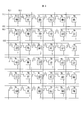
液晶パネルLCPでは、図4(a)(b)に示すように、緑の第1画素Gp(1)の画素電極PE1は、トランジスタTR1を介してデータ信号線SL1および走査信号線GL1に接続され、青の第2画素Bp(2)の画素電極PE2は、トランジスタTR2を介してデータ信号線SL1および走査信号線GL2に接続され、緑の第3画素Gp(3)の画素電極PE3は、トランジスタTR3を介してデータ信号線SL2および走査信号線GL2に接続され、赤の第4画素Rp(4)の画素電極PE4は、トランジスタTR4を介してデータ信号線SL2および走査信号線GL1に接続されている。また、補助容量配線CS1は、画素電極PE1および画素電極PE4それぞれと補助容量を形成し、補助容量配線CS2は、画素電極PE2および画素電極PE3それぞれと補助容量を形成する。
ここで、画素電極PE1には、データ信号線SL1およびトランジスタTR1を介して画素データGd(1)に対応する表示信号gd1が書き込まれ、画素電極PE2には、データ信号線SL1およびトランジスタTR2を介して画素データBd(2)に対応する表示信号bd2が書き込まれ、画素電極PE3には、データ信号線SL2およびトランジスタTR3を介して画素データGd(3)に対応する表示信号gd3が書き込まれ、画素電極PE4には、データ信号線SL2およびトランジスタTR4を介して画素データRd(4)に対応する表示信号rd4が書き込まれる。なお、図4(b)は液晶パネルLCPの一例に過ぎず、例えば図4(c)のような構成でも構わない。
実施例1の液晶表示装置LCDでは、同じ画素数の一般的なサブ画素方式(図4(d)に示すように、第1画素PiX1に対応する輝度信号y1から3つのサブピクセルSR・SG・SBのサブ画素データr1・g1・b1を作成し、第2画素PiX2に対応する輝度信号y2から3つのサブピクセルSR・SG・SBのサブ画素データr2・g2・b2を作成し、第3画素PiX3に対応する輝度信号y3から3つのサブピクセルSR・SG・SBのサブ画素データr3・g3・b3を作成し、第4画素PiX4に対応する輝度信号y4から3つのサブピクセルSR・SG・SBのサブ画素データr4・g4・b4を作成し、12個のサブピクセルを6本のデータ信号線と2本の走査信号線で駆動する方式)の液晶表示装置と比べて、精細感をさほど落とすことなく、データ信号線の数(ソース端子数)を1/3に削減することができる。
さらに、実施例1の液晶表示装置LCDによれば、図2・3に示すように、撮像装置CAMからのDG方式の映像信号IGSを、DG方式の液晶パネルLCPにダイレクトに表示することができるため、一般的なサブ画素方式の液晶表示装置に表示するときに必要な解像度変換等の処理(オリジナル特性を失わせるおそれがある処理)を不要とする、あるいは最小限にとどめることができる。
[実施例2]
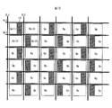
実施例2では、図5~図7に示すように、液晶パネルLCPへの表示信号の書き込み極性を、1画素行では2×i(iは自然数)画素ごとに反転させ、1画素列では2×j(jは自然数)画素ごとに反転させる。ドライバの消費電力や充電率の観点からは、i、jを大きくすることが望ましいが、i、jを大きくすると、フリッカ等の視認によって表示品位が低下する場合がある。
実施例2では、図5~図7に示すように、液晶パネルLCPへの表示信号の書き込み極性を、1画素行では2×i(iは自然数)画素ごとに反転させ、1画素列では2×j(jは自然数)画素ごとに反転させる。ドライバの消費電力や充電率の観点からは、i、jを大きくすることが望ましいが、i、jを大きくすると、フリッカ等の視認によって表示品位が低下する場合がある。
この点、ITU-BT.2020で規定されるようなSHV(スーパーハイビジョン)の視聴では、0.75H(Hは表示部の対角の長さ)の視聴距離で1画素が認識できないことが望ましいとされる。画素数が8K×4Kの液晶パネルを前提にすれば、一般に、視聴距離3Hでは4×4画素分のブロックの認識は不可能で、通常の視聴距離6Hでは8×8画素分のブロックの認識も困難とされる。この認識精度はCRT(インターレース駆動)の1H(横ライン)ストライプ表示に基づいていること、実施例2ではフリッカの単位(プラス極性のブロックとマイナス極性のブロック)が市松配置となることを考慮すると、表示する絵柄にもよるが、例えば視聴距離3Hで8×8画素分のブロックの認識が容易でない場合もある。また、垂直方向(列方向)の分解能と水平配向(行方向)の分解能とでは、一般に水平方向の方が認知精度が高いことも知られている。
以上から、iとjは求められる表示品位と視聴距離によって変化し、通常は、図5のように、i=j=2(4×4画素反転)とし、高品位が必要な場面では、図6のように、i=j=1(2×2画素反転)とし、比較的品位を求められない状況では、i=j=4(8×8画素反転)とする。また、水平方向の認知精度が高いことを考慮して、i<jとすることもできる。例えば、図7のように、i=1、j=2とし、極性のそろった画素を縦長に配置する(フリッカの単位となるブロックを縦長にする)方が、認知性および消費電力双方の観点から有利であり、好ましい。
なお、図5~図7では、隣り合う2本の画素列の一方と他方とで、接続するデータ信号線の配置(左側・右側)を変えているがこれに限定されない。図8のように、隣り合う2本の画素列の一方と他方とで、接続するデータ信号線の配置(左側・右側)を揃える(例えば、同図のように左側に揃える)こともできる。
実施例2では、図9に示すように、液晶表示装置LCDに設けられた設定部SSから表示制御回路DCCに入力される設定信号によって上記iおよびjの少なくとも一方が設定される構成とすることができる。例えば、液晶表示装置LCDと一体化されたユーザ入力部または液晶表示装置LCDとは別体のユーザ入力装置からの指示(ユーザ入力)に応じて、設定部SSが設定信号を生成する構成とする。この場合、ユーザ入力部やユーザ入力装置の一部ボタンを「なめらかさ」などのパラメータに対応させることが好ましい。
また、図10に示すように、液晶表示装置LCDに設けられた人感センサPSから得られた視聴者と画面との距離に応じて、設定部SSが設定信号を生成する構成とすることもできる。
また、図11に示す設定部SSのように、通常は人感センサーPSから得られた視聴者と画面との距離に応じて設定信号を生成する(上記iおよびjの少なくとも一方を自動的に最適値に設定する)が、視聴者が手動設定したいときには、例えばユーザ入力装置LC(リモコン)からのユーザ入力に応じて設定信号を生成するような構成でも構わない。
[実施例3]
実施例3では、図12に示すように、緑の第1画素Gp(1)の有効面積を、青の第2画素Bp(2)の有効面積よりも小さくする。なお、緑の第3画素Gp(3)の有効面積は、緑の第1画素Gp(1)と等しく、赤の第4画素Rp(4)の有効面積は、青の第2画素Bp(2)の有効面積と等しくする。
実施例3では、図12に示すように、緑の第1画素Gp(1)の有効面積を、青の第2画素Bp(2)の有効面積よりも小さくする。なお、緑の第3画素Gp(3)の有効面積は、緑の第1画素Gp(1)と等しく、赤の第4画素Rp(4)の有効面積は、青の第2画素Bp(2)の有効面積と等しくする。
具体的には、緑の第1画素Gp(1)に対応する画素電極の面積は、青の第2画素Bp(2)に対応する画素電極の面積よりも小さく、カラーフィルタの緑の第1画素Gp(1)に対応する部分の面積は、カラーフィルタの青の第2画素Bp(2)に対応する部分の面積よりも小さくしている。
こうすれば、緑の画素の表示信号を相対的に押さえたり、バックライトBLの緑色の輝度を下げるなどの手法と比べて、液晶パネル全体の輝度効率をほとんど下げることなく、画面全体で各色の輝度バランスを設定することができる。また、緑の画素の面積が小さくなることによって先鋭感が増大する効果も得られる。
さらに図12では、緑の第1画素Gp(1)の重心位置(白丸)と緑の第3画素Gp(3)の重心位置(白三角)との距離は、青の第2画素Bp(2)の重心位置(黒三角)と赤の第4画素Rpの重心位置(黒丸)との距離よりも大きい。換言すれば、緑の第1画素Gp(1)と第4画素Rp(4)とが行方向に隣接し、列方向に延伸する2本のデータ信号線SL1・SL2が、第1~第4画素Gp(1)・Bp(2)・Gp(3)・Rp(4)を挟むように設けられ、第1および第2画素Gp(1)・Bp(2)は、データ信号線SL1から同じ距離だけ離れ、第3および第4画素Gp(3)・Rp(4)は、データ信号線SL2から同じ距離だけ離れており、緑の第1画素Gp(1)の行方向(走査信号線と平行な方向)の幅は赤の第4画素Rp(4)の行方向の幅よりも小さく、緑の第3画素Gp(3)の行方向の幅は青の第2画素Bp(2)の行方向の幅よりも小さい。このように、緑の第1画素Gp(1)および緑の第3画素Gp(3)それぞれを小さくし、さらにこれらを離すことで、先鋭感がより増大する。
実施例3では、図13に示すように、緑の第1画素Gp(1)、青の第2画素Bp(2)、緑の第3画素Gp(3)および赤の第4画素Rp(4)それぞれの画素電極の面積を等しくし、カラーフィルタの緑の第1画素Gp(1)および緑の第3画素Gp(3)に対応する部分に遮光領域LBを形成してもよい。
実施例3では、緑の第1画素Gp(1)の画素電極は、略長方形の形状を持つ、青の第2画素Bp(2)の画素電極の一辺または両辺を縮小して得られる形状である。特に高精細の液晶パネルでは、画素電極の辺の途中に切りかけ(三角形や四角形)を形成すると、切りかけ部分の周辺に発生する斜め電界が液晶配向を変化させ、応答制御のし難い液晶パネルになるおそれがある。
そこで、緑に対応する画素電極が、青や赤に対応する画素電極と実質的に相似形あるいは類似形(この場合は長方形)となるように、緑に対応する画素電極の面積を調整する。すなわち、信号線の影響は直線的で補正しやすいため、長方形の画素電極の一辺のみを短くすることで面積を調整する。この場合も、表示への影響を最小限にするため、図12・図13に示すように、走査信号線と平行な辺を短くする方が望ましい。
[実施例4]
実施例4では、バックライトBLは、緑色とそれ以外の色との色バランスが調整可能であり、緑の第1画素Gp(1)の有効面積と青の第2画素Bp(2)の有効面積との比率、または緑の第1画素Gp(1)の有効面積と赤の第4画素Rp(2)の有効面積との比率に応じて上記色バランスが設定される。こうすれば、画素構造によらない設定が容易になる。
実施例4では、バックライトBLは、緑色とそれ以外の色との色バランスが調整可能であり、緑の第1画素Gp(1)の有効面積と青の第2画素Bp(2)の有効面積との比率、または緑の第1画素Gp(1)の有効面積と赤の第4画素Rp(2)の有効面積との比率に応じて上記色バランスが設定される。こうすれば、画素構造によらない設定が容易になる。
バックライトBLは、図14(a)に示すように、赤(R)のLED素子、緑(G)のLED素子、および青(B)のLED素子を含む照明ユニットLUを複数有する直下型のLED照明装置であり、照明制御回路LCCによって各色のLED素子が独立して制御可能であることが望ましい。
また、図14(a)に示すように、バックライトBLは、緑色レーザー発生素子を含むエッジ型の照明ユニットEDLU(LZ)を備え、緑色レーザー光が導光板LGを介して液晶パネルLCPに供給される構成とすることもできる。SHVの規格ITU BT.2020に定められた緑色の再現範囲は、520nm-530nmであり、この波長帯の実現には、緑色レーザーが最適である。なお、赤および青については、図14(b)のようにLED素子を含むエッジ型の照明ユニットEDLU(LED)を用いることができる。もちろん、赤および青についても、レーザ発生素子を含むエッジ型の照明ユニットを用いることができる。
[実施例5]
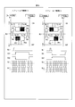
液晶パネルLCPを図15(a)のように構成することもできる。すなわち、緑の第1画素Gp(1)がトランジスタTR1を介して走査信号線GL1およびデータ信号線SL1に接続され、青の第2画素Bp(2)がトランジスタTR2を介して走査信号線GL1およびデータ信号線SL1に接続され、緑の第3画素Gp(3)がトランジスタTR3を介して走査信号線GL1およびデータ信号線SL2に接続され、赤の第2画素Rp(4)がトランジスタTR4を介して走査信号線GL1およびデータ信号線SL2に接続され、補助容量配線CS1が、緑の第1画素Gp(1)および赤の第4画素Rp(4)それぞれと補助容量を形成し、補助容量配線CS2が、青の第2画素Bp(2)および緑の第3画素Gp(3)それぞれと補助容量を形成している。なお、図15(a)の構成では、1本の補助容量配線(例えばCS2)を、隣り合う2つの画素行で共有している。
液晶パネルLCPを図15(a)のように構成することもできる。すなわち、緑の第1画素Gp(1)がトランジスタTR1を介して走査信号線GL1およびデータ信号線SL1に接続され、青の第2画素Bp(2)がトランジスタTR2を介して走査信号線GL1およびデータ信号線SL1に接続され、緑の第3画素Gp(3)がトランジスタTR3を介して走査信号線GL1およびデータ信号線SL2に接続され、赤の第2画素Rp(4)がトランジスタTR4を介して走査信号線GL1およびデータ信号線SL2に接続され、補助容量配線CS1が、緑の第1画素Gp(1)および赤の第4画素Rp(4)それぞれと補助容量を形成し、補助容量配線CS2が、青の第2画素Bp(2)および緑の第3画素Gp(3)それぞれと補助容量を形成している。なお、図15(a)の構成では、1本の補助容量配線(例えばCS2)を、隣り合う2つの画素行で共有している。
実施例5では、図15(b)(c)に示すように、フィールド期間1において、第1画素Gp(1)の輝度を第2画素Bp(2)の輝度よりも高くして、この第1画素Gp(1)の輝度を、輝度信号Y1に基づく第1画素Gp(1)の画素データGd(1)に対応させ、第3画素Gp(3)の輝度を第4画素Rp(4)の輝度よりも高くして、この第3画素Gp(3)の輝度を、輝度信号Y3に基づく第3画素Gp(3)の画素データGd(3)に対応させる。さらに、フィールド期間1に続くフィールド期間2において、図15(b)・(d)・(e)に示すように、第2画素Bp(2)の輝度を第1画素Gp(1)の輝度よりも高くして、この第2画素Bp(2)の輝度を、輝度信号Y2に基づく第2画素Bp(2)の画素データBd(2)に対応させ、第4画素Rp(4)の輝度を第3画素Gp(3)の輝度よりも高くして、この第4画素Rp(4)の輝度を、輝度信号Y4に基づく第4画素Rp(4)の画素データRd(4)に対応させる。
実施例5では、走査信号線GL1、データ信号線SL1・SL2、補助容量配線CS1・CS2を、例えば図16のように駆動する。すなわち、データ信号線SL1・SL2それぞれの極性を1H(水平走査期間)ごとに反転させ、フィールド期間開始時の極性を2フィールドごとに反転させる。また、同一水平走査期間におけるデータ信号線SL1・SL2の極性を逆とする。さらに、補助容量配線CS1・CS2それぞれの電位を一定の周期(例えばnH)で振幅(Low~High)させ、フィールド期間1の走査信号線GL1の選択期間は、補助容量配線CS1の電位を「Low(L)」、補助容量配線CS2の電位を「High(H)」とし、選択期間終了後に、補助容量配線CS1の電位を「H」(突き上げ)、補助容量配線CS2の電位を「L」とし、フィールド期間2の走査信号線GL1の選択期間は、補助容量配線CS1の電位を「H」、補助容量配線CS2の電位を「L」とし、選択期間終了後に、補助容量配線CS1の電位を「L」(突き下げ)、補助容量配線CS2の電位を「H」(突き上げ)とする。
実施例5によれば、図4(d)のような構成に比して、データ信号線数(ソース側の入力端子数)および走査信号線数(ゲート側の入力端子数)それぞれを削減することができる。
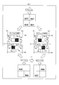
実施例5では、図17(a)に示すように、図15の画素データGd(1)・Bd(2)・Gd(3)・Rd(4)が、図1の映像信号IGSの同一フレームから得られるものであってもよい。また、図17(b)に示すように、図15の画素データGd(1)・Gd(3)が、映像信号IGSのあるフレーム(例えばフレーム1:奇数フレーム)から得られるものであって、画素データBd(2)・Rd(4)が、映像信号IGSの別のフレーム(例えばフレーム2、偶数フレーム)から得られるものであってもよい。
〔まとめ〕
本表示装置は、緑の第1画素、青の第2画素、緑の第3画素、および赤の第4画素がベイヤー配列とされた直視用の表示パネルを備え、第1画素に供給される表示信号のもとになる、第1画素の画素位置に対応する輝度情報と、第3画素に供給される表示信号のもとになる、第3画素の画素位置に対応する輝度情報とが別々のものである構成とすることもできる。
本表示装置は、緑の第1画素、青の第2画素、緑の第3画素、および赤の第4画素がベイヤー配列とされた直視用の表示パネルを備え、第1画素に供給される表示信号のもとになる、第1画素の画素位置に対応する輝度情報と、第3画素に供給される表示信号のもとになる、第3画素の画素位置に対応する輝度情報とが別々のものである構成とすることもできる。
本表示装置は、緑の第1受光部、青の第2受光部、緑の第3受光部、および赤の第4受光部がベイヤー配列とされた撮像素子において上記第1~第4受光部から得られた第1~第4撮像信号それぞれを上記第1~第4画素に表示する構成とすることもできる。
本表示装置は、上記表示パネルは液晶パネルであって、第1画素と第2または第4画素とが列方向に隣接し、データ信号の書き込み極性が、1画素行では2×i(iは自然数)画素ごとに反転し、1画素列では2×j(jは自然数)画素ごとに反転する構成とすることもできる。
本表示装置は、上記iおよびjの少なくとも一方が可変である構成とすることもできる。
本表示装置は、表示装置と一体化されたユーザ入力部、または表示装置とは別体のユーザ入力装置からの指示に応じて上記iおよびjの少なくとも一方を設定する設定部を備える構成とすることもできる。
本表示装置は、人感センサーと、人感センサーから得られた観察者と画面との距離に応じて上記iおよびjの少なくとも一方を設定する設定部とを備える構成とすることもできる。
本表示装置では、液晶パネルのデータ信号線の延伸方向を列方向として、上記iが上記jよりも小さい構成とすることもできる。
本表示装置は、第1画素の有効面積が第2画素の有効面積よりも小さい構成とすることもできる。
本表示装置は、上記表示パネルは液晶パネルであって、第1画素に対応する第1画素電極の面積と第2画素に対応する第2画素電極の面積とが等しく、カラーフィルタの第1画素電極に対向する部分に遮光領域が形成されている構成とすることもできる。
本表示装置は、上記表示パネルは液晶パネルであって、第1画素に対応する第1画素電極の面積は、第2画素に対応する第2画素電極の面積よりも小さく、カラーフィルタの第1画素電極に対向する部分の面積は、カラーフィルタの第2画素電極に対向する部分の面積よりも小さい構成とすることもできる。
本表示装置は、上記第1画素電極は、略長方形の形状を持つ上記第2画素電極の一辺または両辺を縮小して得られる形状である構成とすることもできる。
本表示装置は、第3画素に対応する第3画素電極は、上記第1画素電極と同一形状であり、第4画素に対応する第4画素電極は、上記第2画素電極と同一形状であり、上記第1画素電極の重心位置と上記第3画素電極の重心位置との距離は、上記第2画素電極の重心位置と上記第4画素電極の重心位置との距離よりも大きい構成とすることもできる。
本表示装置は、上記表示パネルは液晶パネルであって、該液晶パネルの背面に設けられた照明装置を備え、該照明装置は、緑色とそれ以外の色との色バランスが調整可能であり、第1画素の有効面積と第2画素の有効面積との比率、または第1画素の有効面積と第4画素の有効面積との比率に応じて上記色バランスが設定される構成とすることもできる。
上記照明装置は、赤のLED素子、緑のLED素子、および青のLED素子を含む直下型のLED照明装置であり、各色のLED素子が独立して制御可能である構成とすることもできる。
本表示装置は、上記照明装置は緑色レーザー発生素子を備え、緑色レーザー光が導光板を介して上記液晶パネルに供給される構成とすることもできる。
本表示装置は、第1画素が第1トランジスタを介して第1走査信号線および第1データ信号線に接続され、第2画素が第2トランジスタを介して上記第1走査信号線および第1データ信号線に接続され、第1画素が第1補助容量配線と補助容量を形成し、第2画素が第2補助容量配線と補助容量を形成している構成とすることもできる。
本表示装置は、第1フィールド期間では、第1画素の輝度が第2画素の輝度よりも高く、第1フィールド期間に続く第2フィールド期間では、第2画素の輝度が第1画素の輝度よりも高い構成とすることもできる。
本表示装置では、第1フィールド期間では、第3画素の輝度が第4画素の輝度よりも高く、第1フィールド期間に続く第2フィールド期間では、第4画素の輝度が第3画素の輝度よりも高い構成とすることもできる。
本表示装置では、第1フィールド期間の第1画素の輝度は、入力される第1フレームの第1画素の映像信号に対応し、第2フィールド期間の第2画素の輝度は、上記第1フレームの第2画素の映像信号に対応する構成とすることもできる。
本表示装置では、第1フィールド期間の第1画素の輝度は、入力される第1フレームの第1画素の映像信号に対応し、第2フィールド期間の第2画素の輝度は、上記第1フレームの後に入力される第2フレームの第2画素の映像信号に対応する構成とすることもできる。
本発明は上記の実施の形態に限定されるものではなく、上記実施の形態を技術常識に基づいて適宜変更したものやそれらを組み合わせて得られるものも本発明の実施の形態に含まれる。
本発明は、特に高解像度ディスプレイに好適である。
10 表示装置
LCD 液晶表示装置
LCP 液晶パネル
BL バックライト
Gp 緑画素
Bp 青画素
Rp 赤画素
Y1~Y4 輝度信号
LCD 液晶表示装置
LCP 液晶パネル
BL バックライト
Gp 緑画素
Bp 青画素
Rp 赤画素
Y1~Y4 輝度信号
Claims (14)
- 緑の第1画素、青の第2画素、緑の第3画素、および赤の第4画素がベイヤー配列とされた直視用の表示パネルを備え、
第1画素に供給される表示信号のもとになる、第1画素の画素位置に対応する輝度情報と、第3画素に供給される表示信号のもとになる、第3画素の画素位置に対応する輝度情報とが別々のものであることを特徴とする表示装置。 - 緑の第1受光部、青の第2受光部、緑の第3受光部、および赤の第4受光部がベイヤー配列とされた撮像素子において上記第1~第4受光部から得られた第1~第4撮像信号それぞれを上記第1~第4画素に表示する請求項1記載の表示装置。
- 上記表示パネルは液晶パネルであって、第1画素と第2または第4画素とが列方向に隣接し、データ信号の書き込み極性が、1画素行では2×i(iは自然数)画素ごとに反転し、1画素列では2×j(jは自然数)画素ごとに反転する請求項1記載の表示装置。
- 上記iおよびjの少なくとも一方が可変である請求項3の表示装置。
- 表示装置と一体化されたユーザ入力部、または表示装置とは別体のユーザ入力装置からの指示に応じて上記iおよびjの少なくとも一方を設定する設定部を備える請求項4記載の表示装置。
- 人感センサーと、人感センサーから得られた観察者と画面との距離に応じて上記iおよびjの少なくとも一方を設定する設定部とを備える請求項4記載の表示装置。
- 第1画素の有効面積が第2画素の有効面積よりも小さい請求項1~6のいずれか1項に記載の表示装置。
- 上記表示パネルは液晶パネルであって、第1画素に対応する第1画素電極の面積と第2画素に対応する第2画素電極の面積とが等しく、カラーフィルタの第1画素電極に対向する部分に遮光領域が形成されている請求項7記載の表示装置。
- 上記表示パネルは液晶パネルであって、第1画素に対応する第1画素電極の面積は、第2画素に対応する第2画素電極の面積よりも小さく、カラーフィルタの第1画素電極に対向する部分の面積は、カラーフィルタの第2画素電極に対向する部分の面積よりも小さい請求項7記載の表示装置。
- 上記第1画素電極は、略長方形の形状を持つ上記第2画素電極の一辺または両辺を縮小して得られる形状である請求項9記載の表示装置。
- 第3画素に対応する第3画素電極は、上記第1画素電極と同一形状であり、第4画素に対応する第4画素電極は、上記第2画素電極と同一形状であり、
上記第1画素電極の重心位置と上記第3画素電極の重心位置との距離は、上記第2画素電極の重心位置と上記第4画素電極の重心位置との距離よりも大きい請求項9記載の表示装置。 - 上記表示パネルは液晶パネルであって、該液晶パネルの背面に設けられた照明装置を備え、該照明装置は、緑色とそれ以外の色との色バランスが調整可能であり、第1画素の有効面積と第2画素の有効面積との比率、または第1画素の有効面積と第4画素の有効面積との比率に応じて上記色バランスが設定される請求項7記載の表示装置。
- 上記照明装置は、赤のLED素子、緑のLED素子、および青のLED素子を含む直下型のLED照明装置であり、各色のLED素子が独立して制御可能である請求項12の表示装置。
- 上記照明装置は緑色レーザー発生素子を備え、緑色レーザー光が導光板を介して上記液晶パネルに供給される請求項12の表示装置。
Priority Applications (1)
| Application Number | Priority Date | Filing Date | Title |
|---|---|---|---|
| US14/907,019 US9805665B2 (en) | 2013-09-20 | 2014-05-26 | Display device |
Applications Claiming Priority (2)
| Application Number | Priority Date | Filing Date | Title |
|---|---|---|---|
| JP2013196029 | 2013-09-20 | ||
| JP2013-196029 | 2013-09-20 |
Publications (1)
| Publication Number | Publication Date |
|---|---|
| WO2015040892A1 true WO2015040892A1 (ja) | 2015-03-26 |
Family
ID=52688555
Family Applications (1)
| Application Number | Title | Priority Date | Filing Date |
|---|---|---|---|
| PCT/JP2014/063847 Ceased WO2015040892A1 (ja) | 2013-09-20 | 2014-05-26 | 表示装置 |
Country Status (2)
| Country | Link |
|---|---|
| US (1) | US9805665B2 (ja) |
| WO (1) | WO2015040892A1 (ja) |
Families Citing this family (1)
| Publication number | Priority date | Publication date | Assignee | Title |
|---|---|---|---|---|
| KR20230103668A (ko) * | 2021-12-31 | 2023-07-07 | 엘지디스플레이 주식회사 | 표시 장치 |
Citations (6)
| Publication number | Priority date | Publication date | Assignee | Title |
|---|---|---|---|---|
| JPS59111196A (ja) * | 1982-12-15 | 1984-06-27 | シチズン時計株式会社 | カラ−表示装置 |
| JP2010204674A (ja) * | 2010-04-02 | 2010-09-16 | Sharp Corp | 液晶表示装置 |
| JP2011099961A (ja) * | 2009-11-05 | 2011-05-19 | Sharp Corp | 表示装置、表示方法、表示プログラム、及びコンピュータ読み取り可能な記録媒体 |
| JP2012053387A (ja) * | 2010-09-03 | 2012-03-15 | Mitsumi Electric Co Ltd | バックライト装置、該バックライト装置を備えた表示装置及び照明装置 |
| JP2012230173A (ja) * | 2011-04-25 | 2012-11-22 | Japan Display East Co Ltd | 表示装置 |
| WO2012169140A1 (ja) * | 2011-06-08 | 2012-12-13 | パナソニック株式会社 | 画像処理装置及び画像処理方法並びにデジタルカメラ |
Family Cites Families (3)
| Publication number | Priority date | Publication date | Assignee | Title |
|---|---|---|---|---|
| JP3365357B2 (ja) | 1999-07-21 | 2003-01-08 | 日本電気株式会社 | アクティブマトリクス型液晶表示装置 |
| JP2006084860A (ja) * | 2004-09-16 | 2006-03-30 | Sharp Corp | 液晶表示装置の駆動方法及び液晶表示装置 |
| US8006002B2 (en) * | 2006-12-12 | 2011-08-23 | Apple Inc. | Methods and systems for automatic configuration of peripherals |
-
2014
- 2014-05-26 US US14/907,019 patent/US9805665B2/en not_active Expired - Fee Related
- 2014-05-26 WO PCT/JP2014/063847 patent/WO2015040892A1/ja not_active Ceased
Patent Citations (6)
| Publication number | Priority date | Publication date | Assignee | Title |
|---|---|---|---|---|
| JPS59111196A (ja) * | 1982-12-15 | 1984-06-27 | シチズン時計株式会社 | カラ−表示装置 |
| JP2011099961A (ja) * | 2009-11-05 | 2011-05-19 | Sharp Corp | 表示装置、表示方法、表示プログラム、及びコンピュータ読み取り可能な記録媒体 |
| JP2010204674A (ja) * | 2010-04-02 | 2010-09-16 | Sharp Corp | 液晶表示装置 |
| JP2012053387A (ja) * | 2010-09-03 | 2012-03-15 | Mitsumi Electric Co Ltd | バックライト装置、該バックライト装置を備えた表示装置及び照明装置 |
| JP2012230173A (ja) * | 2011-04-25 | 2012-11-22 | Japan Display East Co Ltd | 表示装置 |
| WO2012169140A1 (ja) * | 2011-06-08 | 2012-12-13 | パナソニック株式会社 | 画像処理装置及び画像処理方法並びにデジタルカメラ |
Also Published As
| Publication number | Publication date |
|---|---|
| US9805665B2 (en) | 2017-10-31 |
| US20160163270A1 (en) | 2016-06-09 |
Similar Documents
| Publication | Publication Date | Title |
|---|---|---|
| TWI431606B (zh) | 立體顯示器及其驅動方法 | |
| CN102341744B (zh) | 立体显示装置 | |
| CN106297626B (zh) | 多视图显示装置 | |
| US20160048053A1 (en) | Liquid crystal display device and driving method thereof | |
| US9648312B2 (en) | Display device in which multiple images are displayed using four neighboring pixels, display panel and electronic apparatus using same | |
| JP5266573B2 (ja) | 液晶表示装置 | |
| US8587737B2 (en) | Display device | |
| JP5522336B2 (ja) | 液晶表示装置 | |
| US20130027525A1 (en) | Liquid-crystal display device and three-dimensional display system | |
| WO2012039345A1 (ja) | 液晶表示装置、および、ディスプレイ装置 | |
| US20150156482A1 (en) | Three-dimensional (3d) liquid crystal display (lcd) device, 3d lcd display system and 3d image display driving method | |
| JP3559115B2 (ja) | 表示装置 | |
| US9470900B2 (en) | Display unit, display driving circuit, and display driving method | |
| US20130063332A1 (en) | Display device, display method, and electronic apparatus | |
| JP2009244287A (ja) | 液晶表示装置および液晶表示装置の駆動方法 | |
| WO2015040892A1 (ja) | 表示装置 | |
| WO2013047099A1 (ja) | 表示装置 | |
| WO2012043408A1 (ja) | 液晶表示装置、駆動方法、および、ディスプレイ装置 | |
| KR20130073667A (ko) | 액정표시장치와 그를 이용한 입체영상 표시장치 | |
| CN103189791B (zh) | 显示装置 | |
| JP2019015942A (ja) | 表示装置、及び、その駆動方法 | |
| KR101686093B1 (ko) | 시야각 제어 액정 표시 장치 및 이의 구동 방법 | |
| WO2015040880A1 (ja) | 液晶表示装置 | |
| JP2014006363A (ja) | 表示装置および表示装置の駆動方法 | |
| WO2012073795A1 (ja) | 表示装置およびその駆動方法、並びに電子装置 |
Legal Events
| Date | Code | Title | Description |
|---|---|---|---|
| 121 | Ep: the epo has been informed by wipo that ep was designated in this application |
Ref document number: 14845740 Country of ref document: EP Kind code of ref document: A1 |
|
| WWE | Wipo information: entry into national phase |
Ref document number: 14907019 Country of ref document: US |
|
| NENP | Non-entry into the national phase |
Ref country code: DE |
|
| 122 | Ep: pct application non-entry in european phase |
Ref document number: 14845740 Country of ref document: EP Kind code of ref document: A1 |
|
| NENP | Non-entry into the national phase |
Ref country code: JP |