WO2015033700A1 - 発光装置用基板、発光装置、および発光装置用基板の製造方法 - Google Patents
発光装置用基板、発光装置、および発光装置用基板の製造方法 Download PDFInfo
- Publication number
- WO2015033700A1 WO2015033700A1 PCT/JP2014/069745 JP2014069745W WO2015033700A1 WO 2015033700 A1 WO2015033700 A1 WO 2015033700A1 JP 2014069745 W JP2014069745 W JP 2014069745W WO 2015033700 A1 WO2015033700 A1 WO 2015033700A1
- Authority
- WO
- WIPO (PCT)
- Prior art keywords
- substrate
- layer
- emitting device
- light emitting
- reflective layer
- Prior art date
- Legal status (The legal status is an assumption and is not a legal conclusion. Google has not performed a legal analysis and makes no representation as to the accuracy of the status listed.)
- Ceased
Links
Images



Classifications
-
- C—CHEMISTRY; METALLURGY
- C25—ELECTROLYTIC OR ELECTROPHORETIC PROCESSES; APPARATUS THEREFOR
- C25D—PROCESSES FOR THE ELECTROLYTIC OR ELECTROPHORETIC PRODUCTION OF COATINGS; ELECTROFORMING; APPARATUS THEREFOR
- C25D11/00—Electrolytic coating by surface reaction, i.e. forming conversion layers
- C25D11/02—Anodisation
- C25D11/04—Anodisation of aluminium or alloys based thereon
-
- H—ELECTRICITY
- H10—SEMICONDUCTOR DEVICES; ELECTRIC SOLID-STATE DEVICES NOT OTHERWISE PROVIDED FOR
- H10H—INORGANIC LIGHT-EMITTING SEMICONDUCTOR DEVICES HAVING POTENTIAL BARRIERS
- H10H20/00—Individual inorganic light-emitting semiconductor devices having potential barriers, e.g. light-emitting diodes [LED]
- H10H20/01—Manufacture or treatment
-
- H—ELECTRICITY
- H10—SEMICONDUCTOR DEVICES; ELECTRIC SOLID-STATE DEVICES NOT OTHERWISE PROVIDED FOR
- H10H—INORGANIC LIGHT-EMITTING SEMICONDUCTOR DEVICES HAVING POTENTIAL BARRIERS
- H10H20/00—Individual inorganic light-emitting semiconductor devices having potential barriers, e.g. light-emitting diodes [LED]
- H10H20/80—Constructional details
- H10H20/85—Packages
- H10H20/858—Means for heat extraction or cooling
- H10H20/8581—Means for heat extraction or cooling characterised by their material
-
- H—ELECTRICITY
- H10—SEMICONDUCTOR DEVICES; ELECTRIC SOLID-STATE DEVICES NOT OTHERWISE PROVIDED FOR
- H10H—INORGANIC LIGHT-EMITTING SEMICONDUCTOR DEVICES HAVING POTENTIAL BARRIERS
- H10H29/00—Integrated devices, or assemblies of multiple devices, comprising at least one light-emitting semiconductor element covered by group H10H20/00
- H10H29/01—Manufacture or treatment
- H10H29/034—Manufacture or treatment of coatings
-
- H—ELECTRICITY
- H10—SEMICONDUCTOR DEVICES; ELECTRIC SOLID-STATE DEVICES NOT OTHERWISE PROVIDED FOR
- H10H—INORGANIC LIGHT-EMITTING SEMICONDUCTOR DEVICES HAVING POTENTIAL BARRIERS
- H10H29/00—Integrated devices, or assemblies of multiple devices, comprising at least one light-emitting semiconductor element covered by group H10H20/00
- H10H29/01—Manufacture or treatment
- H10H29/036—Manufacture or treatment of packages
- H10H29/0365—Manufacture or treatment of packages of means for heat extraction or cooling
-
- H—ELECTRICITY
- H10—SEMICONDUCTOR DEVICES; ELECTRIC SOLID-STATE DEVICES NOT OTHERWISE PROVIDED FOR
- H10H—INORGANIC LIGHT-EMITTING SEMICONDUCTOR DEVICES HAVING POTENTIAL BARRIERS
- H10H29/00—Integrated devices, or assemblies of multiple devices, comprising at least one light-emitting semiconductor element covered by group H10H20/00
- H10H29/80—Constructional details
- H10H29/85—Packages
- H10H29/855—Optical field-shaping means, e.g. lenses
- H10H29/856—Reflecting means
-
- H—ELECTRICITY
- H10—SEMICONDUCTOR DEVICES; ELECTRIC SOLID-STATE DEVICES NOT OTHERWISE PROVIDED FOR
- H10H—INORGANIC LIGHT-EMITTING SEMICONDUCTOR DEVICES HAVING POTENTIAL BARRIERS
- H10H29/00—Integrated devices, or assemblies of multiple devices, comprising at least one light-emitting semiconductor element covered by group H10H20/00
- H10H29/80—Constructional details
- H10H29/85—Packages
- H10H29/858—Means for heat extraction or cooling
- H10H29/8581—Means for heat extraction or cooling characterised by their material
-
- H—ELECTRICITY
- H10—SEMICONDUCTOR DEVICES; ELECTRIC SOLID-STATE DEVICES NOT OTHERWISE PROVIDED FOR
- H10H—INORGANIC LIGHT-EMITTING SEMICONDUCTOR DEVICES HAVING POTENTIAL BARRIERS
- H10H20/00—Individual inorganic light-emitting semiconductor devices having potential barriers, e.g. light-emitting diodes [LED]
- H10H20/01—Manufacture or treatment
- H10H20/036—Manufacture or treatment of packages
- H10H20/0363—Manufacture or treatment of packages of optical field-shaping means
-
- H—ELECTRICITY
- H10—SEMICONDUCTOR DEVICES; ELECTRIC SOLID-STATE DEVICES NOT OTHERWISE PROVIDED FOR
- H10H—INORGANIC LIGHT-EMITTING SEMICONDUCTOR DEVICES HAVING POTENTIAL BARRIERS
- H10H20/00—Individual inorganic light-emitting semiconductor devices having potential barriers, e.g. light-emitting diodes [LED]
- H10H20/01—Manufacture or treatment
- H10H20/036—Manufacture or treatment of packages
- H10H20/0365—Manufacture or treatment of packages of means for heat extraction or cooling
-
- H—ELECTRICITY
- H10—SEMICONDUCTOR DEVICES; ELECTRIC SOLID-STATE DEVICES NOT OTHERWISE PROVIDED FOR
- H10H—INORGANIC LIGHT-EMITTING SEMICONDUCTOR DEVICES HAVING POTENTIAL BARRIERS
- H10H20/00—Individual inorganic light-emitting semiconductor devices having potential barriers, e.g. light-emitting diodes [LED]
- H10H20/80—Constructional details
- H10H20/85—Packages
- H10H20/855—Optical field-shaping means, e.g. lenses
- H10H20/856—Reflecting means
-
- H—ELECTRICITY
- H10—SEMICONDUCTOR DEVICES; ELECTRIC SOLID-STATE DEVICES NOT OTHERWISE PROVIDED FOR
- H10W—GENERIC PACKAGES, INTERCONNECTIONS, CONNECTORS OR OTHER CONSTRUCTIONAL DETAILS OF DEVICES COVERED BY CLASS H10
- H10W90/00—Package configurations
- H10W90/701—Package configurations characterised by the relative positions of pads or connectors relative to package parts
- H10W90/751—Package configurations characterised by the relative positions of pads or connectors relative to package parts of bond wires
- H10W90/753—Package configurations characterised by the relative positions of pads or connectors relative to package parts of bond wires between laterally-adjacent chips
Definitions
- the present invention is a substrate for a light emitting device that realizes high heat dissipation, a substrate provided with a structure that protects against a plating solution in an electrode pattern plating process, a light emitting device using the substrate, and manufacture of the substrate Regarding the method.
- the basic functions required for a light emitting device substrate include high reflectivity, high heat dissipation, and long-term reliability.
- a typical substrate having these functions is a ceramic substrate, for example, which is manufactured by forming an electrode pattern on a plate-shaped ceramic.
- the ceramic substrate has been getting larger year by year.
- a general LED light-emitting device used at an input power of 30 W is realized by arranging blue LED elements of about 500 ⁇ m ⁇ 800 ⁇ m in size or before and after that on a single substrate, which are classified as medium size, 100 About several LED elements are required.
- a ceramic substrate on which this number of LED elements are arranged for example, there is a substrate having a planar size of 20 mm ⁇ 20 mm or more and a thickness of about 1 mm.
- ceramics are basic ceramics, there is a problem in strength when they are enlarged. If the substrate is thickened to overcome this, the thermal resistance increases and the weight also increases, and the material cost of the substrate also increases. Further, when the ceramic substrate is increased in size, not only the outer dimensions but also the dimensions of the electrode pattern formed on the substrate are likely to go wrong. As a result, it tends to lead to a decrease in manufacturing yield and an increase in manufacturing cost.
- a conventional substrate has a structure in which a light emitting element mounting surface of a metal substrate is covered with a ceramic layer, and a surface opposite to the light emitting element mounting surface (back surface) is exposed to ensure heat dissipation.
- a structure in which a light emitting element mounting surface of a metal substrate is covered with a ceramic layer, and a surface opposite to the light emitting element mounting surface (back surface) is exposed to ensure heat dissipation.
- high heat dissipation can be realized by bringing the metal surface on the back surface of the substrate into close contact with the heat sink via heat dissipation grease.
- An electrode pattern is formed on the ceramic layer on the light emitting element mounting surface in order to establish electrical connection with the light emitting element.
- a circuit pattern is drawn by printing or the like using a metal paste made of a resin containing metal particles, and dried to prepare a base circuit pattern.
- the coating resin layer covering the surface of the base circuit pattern is removed by etching, and the conductive layer is exposed.
- an electrode metal is deposited on the base circuit pattern by plating to complete the electrode pattern.
- the biggest problem in the conventional substrate manufacturing process is a plating process for forming an electrode pattern.
- a plating process for the purpose of protecting the metal substrate from the plating solution used in the plating process, it is necessary to cover the metal surface of the substrate with a protective sheet as a pre-processing step, and as a post-processing step, a protective sheet is used to ensure the heat dissipation of the substrate. It is necessary to remove. If the plating process is performed with the metal surface on the back surface of the metal substrate exposed, omitting the step of covering with the protective sheet, the back surface of the metal substrate is not only affected by the plating solution, but also the same as the electrode pattern such as Au. Precious metal will be deposited and coated.
- a solution that can be easily conceived for the above problem is the introduction of a device that automatically attaches / detaches the protective sheet.
- a device that automatically attaches / detaches the protective sheet there is no such general-purpose automation device, and it is usually an unrealistic choice for manufacturing a substrate for a light-emitting device, which is naturally low in cost.
- a possible solution is to use a special protective sheet. That is, if there is a protective sheet that has chemical resistance, is not eroded by the plating solution, and does not deposit the plating solution, and has high thermal conductivity, and can guarantee long-term reliability, at least, As long as it is attached to the substrate, there is no need to remove it after the plating process.
- an object of the present invention is to provide a substrate having a function of protecting a substrate, not deteriorating a function required for a light emitting device, and having excellent mass productivity, a method for manufacturing the substrate, and A light-emitting device including the substrate is provided.
- a light-emitting device substrate is a light-emitting device substrate in which an insulating reflective layer that reflects light from a light-emitting element is formed on a base body made of aluminum.
- the surface of the substrate other than the surface on which the reflective layer is formed is covered with an anodic oxide film of aluminum.
- an insulating thermal conductive layer having a higher thermal conductivity than the reflective layer may be interposed between the base and the reflective layer.
- the surface of the base made of aluminum other than the surface on which the reflective layer is formed is covered with the anodized film of aluminum. Therefore, the base can be protected from the plating solution or the like in the substrate manufacturing process by the anodized film of aluminum. Furthermore, the coating does not need to be peeled from the substrate because it does not impair an important function for a light-emitting device, that is, high heat dissipation and long-term reliability. Therefore, the substrate and apparatus after manufacture can be protected by leaving. In other words, the coating film can be used both as a process protective film and a device protective film. Moreover, since a film can be formed by anodizing, it is excellent in mass productivity.
- (A) is a top view of the light-emitting device of one Embodiment of this invention, (b) is the sectional drawing.
- (A) is a top view of the board
- (A)-(d) is a figure explaining the manufacturing process of the board
- (A) It is an overhead view of the illuminating device to which the light-emitting device of one Embodiment of this invention is applied, (b) is the sectional drawing.
- FIG. 1 is a figure explaining the manufacturing process of the board
- FIG. 2 is a figure explaining the manufacturing process of the board
- FIG. 2 is a figure explaining the manufacturing process of the board
- FIG. 2 is a figure explaining the manufacturing process of the board
- FIG. 2 is a figure explaining the manufacturing process of the board
- FIG. is a schematic diagram of the light-emitting device of the modification 2 of one Embodiment of this invention. It is sectional drawing of the board
- (A)-(d) is a figure explaining the manufacturing process of the board
- FIG. (A)-(d) is a figure explaining the continuation of the manufacturing process of the board
- FIGS. 2A and 2B are a plan view and a cross-sectional view of a substrate (light emitting device substrate) 5 of the present embodiment.
- FIG. 2C is an enlarged view of a cross section of the substrate 5.
- the substrate 5 is used for a light-emitting device in which a light-emitting element is disposed thereon.
- An example of the light-emitting device is shown in FIG. As in any drawing, dimensions, shapes, numbers, etc. are not necessarily the same as those of an actual substrate, light emitting element, and light emitting device.
- a light-emitting device using the substrate 5 will be described in Embodiment 3.
- a thin film layer (reflection layer) 17 and an electrode pattern 20 are formed on an aluminum base (base) 10.
- a protective layer (aluminum anodic oxide film) 19 is formed on the surface of the aluminum substrate 10 other than the surface on which the thin film layer 17 is formed. That is, the upper surface of the aluminum substrate 10 is covered with the thin film layer 17, and the back surface (the surface opposite to the surface on which the thin film layer 17 is formed) of the aluminum substrate 10 is covered with the protective layer 19.
- the side surface of the aluminum substrate 10 is covered with the thin film layer 17, but instead, it may be covered with a protective layer 19 as shown in FIG. 7.
- an electrode pattern 20 is formed on the thin film layer 17.
- the electrode pattern 20 is composed of a base circuit pattern (not shown) made of a conductive layer and plating (not shown) covering it.
- the electrode pattern 20 is a wiring for establishing electrical connection with a light emitting element disposed on the substrate 5.
- an aluminum plate having a length of 50 mm, a width of 50 mm, and a thickness of 3 mm can be used.
- Advantages of aluminum include light weight, excellent workability, and high thermal conductivity.
- the aluminum substrate 10 may contain components other than aluminum that do not interfere with the anodizing treatment described later.
- the thin film layer 17 is made of an insulating material that reflects light from the light emitting element.
- the thin film layer 17 is formed of a thin film containing ceramics.
- the thin film layer 17 may be formed of a mixture of ceramics and glass, a mixture of ceramics and resin, or ceramics. Since ceramics has high electrostatic pressure resistance, it is possible to prevent a short circuit between the aluminum substrate 10 and the electrode pattern 20.
- the film thickness of the thin film layer 17 is preferably about 50 ⁇ m to 500 ⁇ m, for example, in consideration of the reflectance of the substrate 5. In consideration of thermal resistance, it is desirable that the film thickness be about 50 ⁇ m to 150 ⁇ m. In addition, since it will become easy to produce a crack in the thin film layer 17 when the film thickness of the thin film layer 17 exceeds 1 mm, it is desirable that the film thickness be 1 mm or less.
- the protective layer 19 is an aluminum oxide film (alumite).
- the advantages of anodized are as follows. It can be easily formed on the aluminum surface by anodization. Thermal conductivity is relatively high (several tens W / (m ⁇ K)), lower than metal, but much higher than glass or resin. It has chemical resistance and is stable even at high temperature and high humidity. Even if the layer thickness is thin (several ⁇ m to several tens ⁇ m), it functions as a protective layer.
- the protective layer 19 is a structure introduced for the purpose of protecting the substrate from the plating solution during the plating process for forming the electrode pattern 20 as will be described later, and functions as a layer for preventing corrosion due to oxidation of the aluminum substrate 10.
- the purpose is to do. For this reason, even if it passes through the plating process which forms the electrode pattern 20, it leaves on the base
- an aluminum substrate 10 (for example, 50 mm in length and 50 mm in width) is cut out from an aluminum plate (for example, 3 mmt), and a thin film layer 17 is formed on the upper surface and side surfaces of the aluminum substrate 10 as shown in FIG. (Thin film layer forming step, reflective layer forming step) As shown in FIG. 3B, the protective layer 19 is formed on the back surface of the substrate (protective layer forming step, film forming step). A protective layer 19 may be formed on the side surface of the aluminum substrate 10 instead of the thin film layer 17. In an anodic oxidation process in the protective layer 19 forming step described later, the exposed portion of the aluminum substrate 10 excluding the portion covered with the thin film layer 17 becomes the protective layer 19.
- a raw material may be applied on the aluminum substrate 10 and then fired.
- a ceramic coating containing high-temperature fired ceramic particles and a glass raw material is applied to the aluminum substrate 10, and then glass is synthesized from the glass raw material by a sol-gel method to form the thin film layer 17. Is desirable.
- a glass binder can be formed at a relatively low temperature of 250 to 400 ° C. for this type of layer.
- the temperature for firing the ceramic raw material is usually as high as 1200 to 1400 ° C. Also, when firing ceramic coatings containing ceramic particles that have been fired at a high temperature in a normal glass binder, the firing temperature of the glass is as high as about 900 ° C. Since the melting point of aluminum is about 660 ° C., it cannot withstand such a high-temperature process, so a method of synthesizing glass from a glass raw material by a sol-gel method is adopted. In this method, since a firing temperature of 250 to 400 ° C. and a process temperature lower than the melting point of aluminum of about 660 ° C. can be realized, aluminum can be used as a substrate for the first time.
- the glass component used as a binder has heat resistance, light resistance, and electrostatic pressure resistance like ceramics, it is desirable as a reflective material for lighting devices.
- a stable substance such as glass is desirable because heat generation and light emission of the light source are severe conditions.
- the thin film layer 17 may be formed by applying a thermosetting resin containing ceramic particles to the aluminum substrate 10 and then drying and curing.
- a thermosetting resin a resin having high heat resistance and high light resistance is used in order to prevent deterioration with time and occurrence of discoloration due to heat generated by a light source or strong light irradiation by blue light or the like.
- a resin that is resistant to an acid used in the plating solution and the anodizing treatment is used.
- a thermosetting resin has been described as an example, but it is not limited to a thermosetting resin.
- a thermoplastic resin may be used, and specific materials include silicone resin, epoxy resin, polyimide resin, and fluorine resin. Etc.
- typical materials used as the ceramics or ceramic particles include alumina, zirconia, titanium oxide, and aluminum nitride.
- the ceramics referred to here are not limited to metal oxides, but include ceramics in a broad sense including aluminum nitride and the like, that is, inorganic solid materials in general. Of these inorganic solid materials, any material can be used as long as it is a stable material with excellent heat resistance and light resistance, such as alumina, zirconia, titanium oxide, and aluminum nitride, and is excellent in light diffusion and light reflection. It does n’t matter.
- ceramic materials having high light reflectivity include typical inorganic white materials such as magnesium oxide, zinc oxide, barium sulfate, zinc sulfate, magnesium carbonate, calcium carbonate, wollastonite and the like.
- the particles made of the ceramic material may be appropriately selected and used in combination.
- thermosetting resin Although the long-term reliability of the thin film layer 17 fixed on the aluminum substrate 10 by the thermosetting resin is lower than that of the thin film layer 17 fixed by the glass binder, it is easy at a relatively low temperature of 200 ° C. or less. A thin film layer 17 can be formed. As a result, damage to the aluminum substrate due to heat can be prevented and the manufacturing cost can be reduced.
- the process temperature is low, and the degree of freedom of the process procedure is increased. That is, when the thin film layer forming step is performed at a relatively low temperature of 200 ° C. or lower as described above, it is not necessary to cause the generation of cracks in the protective layer.
- the protective layer forming step is related to the thin film layer forming step. Both are better.
- substrate for light-emitting devices which formed the thin film layer 17 fixed with a thermosetting resin is employable according to a use purpose or a use application.
- the protective layer 19 is formed by anodizing (alumite treatment) of aluminum.
- the protective layer 19 can be formed by subjecting the back surface to alumite treatment. Thereby, it is possible to form the protective layer 19 made of an anodized film of aluminum that is very hard and excellent in durability.
- the thermal conductivity of alumite is approximately 67 W / (m ⁇ K).
- the thermal conductivity of aluminum is only about 1/3 compared to 236W / (m ⁇ K), but about 1W / (m ⁇ K) of glass, silicone resin 0.15-0.30W / (m ⁇ K) Compared to the above, it can be said that the thermal conductivity is overwhelmingly high. Further, the thickness of the normally used alumite film is about 5 to 10 ⁇ m, and even when it is thick, it is about 30 ⁇ m.
- thermal resistance in the case where a 100 ⁇ m thick vitreous layer is formed on the surface of an aluminum substrate 10 having a length of 50 mm, a width of 50 mm, and a thickness of 3 mm as assumed here, and a 30 ⁇ m thick alumite film on the back surface is estimated by the thermal conductivity.
- the thermal resistance in the thickness direction of the substrate decreases by one digit in order of 0.04 K / W, 0.0051 K / W, and 0.00018 K / W in the order of the vitreous layer, the aluminum substrate, and the alumite film.
- the temperature rise in each layer is 4 ° C., 0.51 ° C., and 0.02 ° C. in order. From the above, even when the influence of the alumite film is estimated to be the highest, it is smaller than the other two layers, and its influence on the thermal resistance and temperature rise can be ignored.
- the adverse effect that can be caused by the protective layer 19 formed by the alumite treatment is an increase in thermal resistance.
- the influence is minor and sufficiently negligible compared to the thermal resistance that occurs in other layers. .
- the back surface of the aluminum substrate 10 is covered with a protective layer 19 made of alumite that is extremely hard and has excellent durability due to the alumite treatment, so that the reliability of the substrate is improved. Is much bigger.
- a sealing process is performed after the anodizing process to close the porous holes generated in the anodic oxide film of aluminum which is the protective layer 19.
- the sealing treatment may be performed in accordance with a normal method in this field, and a typical method includes sealing treatment in boiling water. That is, after forming the anodized film, it is sufficiently washed with water and kept in heated pure water for about 30 minutes. In this method, since a large number of substrates 5 can be processed at a time, workability is high.
- the protective layer forming step by anodizing is performed after the thin film layer forming step.
- the ceramic coating containing the ceramic particles fired at high temperature and the glass raw material is applied to the aluminum substrate 10, and then the glass is synthesized from the glass raw material by the sol-gel method to form the thin film layer 17.
- the firing temperature at this time is 250 to 400 ° C. lower than the melting point of aluminum of about 660 ° C.
- the protective layer 19 When the protective layer 19 is heated to this temperature and fired, the protective layer 19 is cracked (cracked), and the function of protecting the substrate from the plating solution during the plating process for forming the electrode pattern is significantly reduced.
- the function of the protective substrate as a protective film is similarly reduced.
- the thin film layer 17 containing ceramics serves as a mask for the alumite treatment in the protective layer forming step. Thereby, only the exposed portion of the aluminum-based material excluding the thin film layer 17 on the aluminum substrate 10 is covered with the protective layer 19.
- the protective layer forming step by anodizing is more preferably performed after the thin film layer forming step.
- the aluminum base 10 is partially alumite treated in the protective layer forming step, or the protective layer forming step
- the anodic oxide film in the region where the thin film layer 17 is formed must be removed. Both of these processes are difficult, and the number of processes that are useless to realize is increased and the manufacturing becomes complicated. For this reason, in order to reduce the manufacturing effort and simplify the manufacturing process, it is desirable to perform the protective layer forming process after the thin film layer forming process.
- the substrate 5 in which the aluminum substrate 10 is covered with the thin film layer 17 and the protective layer 19 is manufactured. Further, the electrode pattern 20 is formed on the thin film layer 17 as follows.
- a metal paste made of a resin containing metal particles is used as a base of the electrode pattern 20, and a circuit pattern is drawn by printing or the like and dried to form a base circuit pattern 22 (Underlying circuit pattern forming step, conductive layer forming step). Since the surface of the underlying circuit pattern 22 is thinly covered with the coating resin layer included in the metal paste, the plating does not precipitate as it is. Therefore, the coating resin layer is removed by etching to expose the conductive layer of the underlying circuit pattern 22, and as shown in FIG. 3D, the electrode metal is deposited on the underlying circuit pattern by plating, The electrode pattern 20 is formed (electrode pattern formation process).
- the aluminum substrate 10 is already covered with a high-reflectance thin film layer 17 containing ceramics and a protective layer 19 of an anodized film. Therefore, the electrode metal can be efficiently deposited from the plating solution only on the base circuit pattern without the aluminum substrate 10 being eroded by the plating solution used in the plating process in the electrode pattern forming step.
- the protective layer 19 is an aluminum oxide film, the thermal resistance is negligibly small. For this reason, it is not necessary to peel off in order to ensure the heat dissipation of the substrate even after the end of the plating process, and a necessary peeling step can be omitted in the protective sheet. Rather, it is desirable to leave the protective layer 19 in order to impart durability and corrosion resistance to the aluminum substrate 10.
- the substrate 5 has a function of protecting the aluminum base 10. And the function requested
- the thin film layer 17 which is a reflective layer may have a two-layer structure. Therefore, in the following, referring to FIGS. 8 and 9, as a first modification of the first embodiment, a substrate having a two-layer structure in which the thin film layer 17 is composed of a lower layer (lower thin film layer 17a) and an upper layer (upper thin film layer 17b). (Light Emitting Device Substrate) 5A will be described. In addition, the same code
- a lower thin film layer 17a, an upper thin film layer 17b, and an electrode pattern 20 are formed on the aluminum base 10 in the order described.
- a protective layer 19 is formed on the back and side surfaces of the aluminum substrate 10.
- the lower thin film layer 17a is made of a material having a lower thermal conductivity than the upper thin film layer 17b
- the upper thin film layer 17b is made of a material having a higher reflectance than the lower thin film layer 17a.
- the lower thin film layer 17a an insulating layer (thermal conductive layer) having a higher thermal conductivity than the upper thin film layer 17b
- the upper thin film layer 17b is an insulating layer (reflective layer) having a higher reflectance than the lower thin film layer 17a.
- the lower thin film layer 17a is formed on the upper surface of the aluminum substrate 10 (lower thin film layer forming step, thermal conductive layer forming step), and the upper thin film layer is formed thereon (upper portion).
- the lower thin film layer 17a and the upper thin film layer 17b may be formed in accordance with the method for forming the thin film layer 17 of the first embodiment. However, ceramic particles are sprayed onto the aluminum substrate 10 at a high speed to form a ceramic deposited layer.
- the lower thin film layer 17a and the upper thin film layer 17b may be formed.
- Typical examples of such a forming method include a thermal spraying method and an AD method (aerosol deposition method).
- the thermal spraying method is subdivided by a particle jet method, and examples thereof include a plasma spraying method, a high-speed flame spraying method, and a cold spray method.
- the method for forming the thin film layer 17 shown in the first embodiment and the above-described thermal spraying method or AD method may be used in appropriate combination.
- an alumina layer is formed as the lower thin film layer 17a using a thermal spraying method, and a ceramic coating containing ceramic particles and glass raw material fired at a high temperature is applied to the lower thin film layer 17a as the upper thin film layer 17b.
- glass may be synthesized by a sol-gel method to form a mixed layer of glass and ceramics.
- the lower thin film layer 17a formed using the thermal spraying method is an alumina deposition layer that does not contain glass as a binder
- the lower thin film layer 17a is an insulating layer (thermal conductive layer) having a higher thermal conductivity than the upper thin film layer 17b. be able to.
- the formation method of the thin film layer 17 shown in Embodiment Mode 1 is used for forming the upper thin film layer 17b, an insulating reflective layer having a high reflectance can be easily formed.
- the protective layer 19 is formed on the side surface and the back surface of the aluminum substrate 10 (protective layer forming step).
- the firing temperature is 250 to 400 ° C. Therefore, in order to avoid the occurrence of cracks (cracks, cracks) in the protective layer 19 due to high temperature, the protective layer 19 is preferably formed after the formation of the lower thin film layer 17a and after the formation of the upper thin film layer 17b.
- a base circuit pattern 22 is formed (base circuit pattern forming step, conductive layer forming step), and as shown in FIG. 9D, the base circuit pattern 22 is formed on the base circuit pattern.
- the electrode metal is deposited to form the electrode pattern 20 (electrode pattern forming step).
- the lower thin film layer 17a may be formed by a method other than the method described above.
- a coating material containing ceramic particles and a glass raw material is applied to the aluminum base 10, and glass is synthesized from the glass raw material by a sol-gel method. You may form as a ceramic layer which consists of a mixture of glass and glass.
- a coating containing ceramic particles and a resin may be applied to the aluminum substrate 10 and cured to form a ceramic layer made of a mixture of ceramic and resin. Alternatively, it may be formed by pasting a ceramic layer made of a mixture of a ceramic and a resin into a sheet shape on the aluminum substrate 10 in advance.
- the upper thin film layer 17b may be formed as a ceramic layer made of a mixture of ceramic and resin by applying a coating containing ceramic particles and resin onto the lower thin film layer 17a and curing.
- a resin such as a silicone resin
- it can be easily cured at a relatively low temperature of 200 ° C. or lower, so that the upper thin film layer 17b can be formed without causing a crack in the protective layer 19.
- the protective layer 19 can be formed not only after the upper thin film layer 17b but also before the upper thin film layer 17b.
- a portion corresponding to the electrode pattern 20 may be partially embedded in the upper thin film layer 17b.
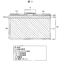
- the electrode pattern 20A when used as a flip-chip type light emitting substrate, most of the electrode pattern 20A is embedded in the upper thin film layer 17b which is an insulating reflective layer, except for the electrode terminal portion to which the electrode of the light emitting element is connected. It is desirable to increase the reflectance of light on the substrate. Therefore, in the following, with reference to FIGS. 10 to 13, as a second modification of the first embodiment, a substrate (light emitting device substrate) 5B in which a part of the electrode pattern 20A is embedded in the upper thin film layer 17b and the same The light emitting device 4A used will be described.
- symbol is attached
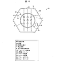
- the light emitting device 4A of the second modification is a flip chip type light emitting device, and a light emitting element 6 is formed on a substrate 5B by flip chip bonding.
- the light emitting element 6 is electrically connected to an electrode pattern 20A formed on the substrate 5B.
- a sealing resin peripheral frame body 8 surrounding the periphery of the light emitting element 6 is provided, and the light emitting element 6 is sealed by filling the sealing resin peripheral frame body 8 with the sealing resin 7. ing.
- the shape and number of each structural member are not limited to what was illustrated.
- the light emitting device 4A includes an anode electrode 37, a cathode electrode 38, an anode mark 39, and a cathode mark 40.
- the anode electrode 37 and the cathode electrode 38 are electrodes for supplying a current for driving the light emitting element 6 and are provided in the form of lands.
- the anode electrode 37 and the cathode electrode 38 are electrodes that can be connected to an external power source (not shown) in the light emitting device 4A.
- the anode electrode 37 and the cathode electrode 38 are connected to the light emitting element 6 through the electrode pattern 20A.
- the anode mark 39 and the cathode mark 40 are alignment marks serving as references for positioning with respect to the anode electrode 47 and the cathode electrode 48, respectively.
- the lower thin film layer 17a, the electrode pattern 20A, and the upper thin film layer 17b are formed on the aluminum base 10 in the order of description. A part is embedded in the layer 17b.
- a protective layer 19 is formed on the back surface of the aluminum substrate 10. Although not shown, it is assumed that a protective layer is also formed on the side surface of the aluminum substrate 10.
- the lower thin film layer 17a is formed on the upper surface of the aluminum base 10 by high-speed flame spraying (lower thin film layer forming step by thermal spraying).
- the exposed portion of the aluminum substrate 10 other than the lower thin film layer 17a, that is, the exposed portion of the aluminum base 10 is covered with a protective layer 19 (protective layer forming step).
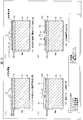
- a metal conductive layer is formed on the lower thin film layer 17a by high-speed flame spraying (metal conductive layer forming step by thermal spraying), and as shown in FIG.
- the conductive layer is flattened (metal conductive layer flattening step). Then, as shown in FIG. 13 (a), a resist 13 is formed on the metal conductive layer at a location to be an electrode terminal portion (light emitting element mounting electrode post) (resist forming step), and FIG. 13 (b). As shown in FIG. 2, the metal conductive layer is half-etched (light emitting element mounting electrode post forming step). Thereafter, the resist 13 is removed. Further, as shown in FIG. 13C, a resist 15 is placed on the metal conductive layer and etched to form an electrode pattern 20A (electrode pattern forming step), and the resist 15 is removed.
- the whole electrode pattern 20A is coat
- the upper thin film layer 17b may be formed in the same manner as in the first modification.
- the electrode terminal portion of the electrode pattern 20A is covered with Au / Ni or Au / Pd / Ni. Need to be. For this reason, the plating 21 is required at the electrode terminal portion, but the aluminum base 10 is already covered and protected by the lower thin film layer 17a and the protective layer 19, and therefore is not subject to erosion by the plating solution or the like. .
- the present invention is not limited to this. Even if the electrode pattern 20A is partially covered by the lower thin film layer 17a, the electrode pattern 20A may be covered only by the upper thin film layer 17b without contacting the lower thin film layer 17a.
- the substrate 5 was manufactured in the order of thin film layer formation, protective layer formation, sealing treatment, foundation circuit pattern formation, coating resin layer removal of the foundation circuit pattern, and electrode pattern formation.
- the substrate 5 is manufactured in the order of thin film layer formation, underlying circuit pattern formation, protective layer formation, sealing treatment, and electrode pattern formation. That is, in the present embodiment, the steps (processing order) of the method for manufacturing the substrate 5 are different from those in the first embodiment. Since the configuration of the substrate 5 is the same, the description thereof is omitted.
- the covering resin layer covering the underlying circuit pattern is removed by etching or the like to ensure conductivity.
- an acidic liquid such as an aqueous sulfuric acid solution is usually used as the processing liquid. Therefore, it is possible to simultaneously remove the coating resin layer and form the protective layer by selecting a substance that is appropriately soluble in the acidic liquid as a binder for the conductive paste.
- the metal paste for forming the underlying circuit pattern and the acidic treatment liquid are appropriately used so that the coating resin layer is appropriately eroded by the acidic treatment liquid used for forming the protective layer.
- the coating resin layer removal of the underlying circuit pattern can be performed together with the protective layer formation.
- the manufacturing process removing the covering resin layer of the underlying circuit pattern
- the insulating liquid covering the conductive layer may not be sufficiently removed with the acidic liquid used as the processing liquid in the anodizing treatment.
- a step of removing the insulating film covering the conductive layer may be added, or the order may be returned to a standard order. That is, after performing the film formation process by anodization, you may perform in order of a conductive layer formation process, the removal process of the insulating film which covers a conductive layer, and an electrode pattern formation process.
- one large base body that can cut out a plurality of the substrates 5 described in the first or second embodiment is prepared, and at the final stage of manufacturing the substrate (a collection of 5 of the plurality of substrates) Turn into. Since a plurality of substrates 5 can be manufactured at a time, efficiency is high.
- an aluminum plate (base body) 24 is prepared and cut in advance so that it can be easily cut at the time of subsequent division. It is not necessary to make a cut. And each process in the manufacturing process of the board
- each small area in FIG. 6A is finished up to the light emitting device, and has a plurality of light emitting regions (light emitting devices) without being cut.
- the light emitting module may be used as it is in the shape of FIG.
- FIGS. 1A and 1B show a plan view and a front sectional view of the light emitting device 4 of the present embodiment.
- the number of light emitting elements 6 is greatly omitted for the sake of simplicity.
- the light emitting device 4 is a COB (chip on board) type light emitting device in which a plurality of light emitting elements 6 such as LED elements and EL elements are mounted on the substrate 5 described in any of the first to third embodiments.
- COB chip on board
- a sealing resin peripheral frame 8 surrounding the periphery of the plurality of light emitting elements 6 is provided on the substrate 5.
- the light emitting elements 6 are sealed by filling the sealing resin peripheral frame 8 with the sealing resin 7.
- the sealing resin 7 contains a phosphor for the purpose of exciting the phosphor with the light emitted from the light emitting element 6 and converting it to light of different wavelengths.
- the light emitting element 6 emits light on the surface of the sealing resin 7.
- the light-emitting elements 6, 10 W, 50 W, 100 W, or 100 W or more is used as input power to the light-emitting device 4 to obtain high-luminance outgoing light.
- the number of light emitting elements 6 is about 300 to 400. It is necessary to accumulate a large number. Since the heat generation of the light emitting device 4 is increased by integrating a large number, the heat sink 2 having a very large volume as compared with the light emitting device 4 as shown in FIG.
- the light emitting element 6 for example, a blue LED, a purple LED, an ultraviolet LED, or the like can be used.
- the phosphor filled in the sealing resin 7 for example, any one color of blue, green, yellow, orange, and red, or a combination of arbitrary plural phosphors can be used. As a result, it is possible to emit emitted light of a desired color from the light emitting device 4.
- the phosphor of the sealing resin 7 may be omitted, and the light emitting elements 6 of three colors of blue, green and red having different emission wavelengths may be arranged on the substrate 5, or any combination of two colors may be used. Alternatively, it may be a single color.
- the light-emitting device 4 uses a substrate 5 that has a function of protecting the substrate from the plating solution and an important function for the light-emitting device and is excellent in mass productivity. Therefore, the high-intensity light emitting device 4 can be manufactured at a reduced cost. Therefore, according to this embodiment, a high-quality light-emitting device can be provided at low cost.
- the light emitting device 4 can be applied to, for example, the lighting device 1 as shown in FIG. 5, and the lighting device 1 is manufactured using the light emitting device 4 that is high quality and inexpensive.
- the lighting device 1 can be provided.
- the protective layer 19 is formed of the same ceramic layer as the thin film layer 17, the same protective function as described in the first to third embodiments can be obtained.
- the protective layer 19 is a substrate having the same material and the same thickness as the thin film layer 17, the only difference from the substrate in which the protective layer 19 is formed of anodized is the thermal resistance in the direction perpendicular to the substrate. Therefore, the thermal resistance is considered below.
- the thermal conductivity of anodized is about 67 W / (m ⁇ K), and the thermal conductivity of glass is about 1 W / (m ⁇ K).
- the thickness of the normally used alumite film is about 30 ⁇ m even when it is thick, whereas the thickness of the vitreous layer as the thin film layer 17 is 100 ⁇ m.
- the thermal resistance in the substrate thickness direction is 0.00018 K / W and 0.04 K / W, respectively.
- 100 W of heat is generated uniformly over the entire surface of the substrate, the temperature rise in the protective layer 19 is negligible at 0.02 ° C. for anodized, whereas it is 4 ° C. for the vitreous layer.
- an alumite film can lower the temperature of the active layer of the light emitting element than the ceramic layer.
- the ceramic layer used for the protective layer 19 has been described using the same material as the thin film layer 17.
- the composition may be different from that of the thin film layer 17.
- ceramics substantially does not enter, and a layer of only glass may be used.
- the protective layer 19 may be any material as long as it functions as a protective layer of the light emitting device 4 and at the same time functions as a protective layer in the substrate manufacturing process.
- the thickness of the protective layer 19 and the thin film layer 17 may be different.
- an insulating reflective layer that reflects light from the light emitting element is formed on a base body (aluminum base body 10) made of aluminum.
- a base body aluminum
- an anodized aluminum film protective layer 19
- the substrate since the surface of the substrate made of aluminum other than the surface on which the reflective layer is formed is covered with the anodized aluminum film (alumite), the substrate can be protected with this film.
- Anodized has excellent chemical resistance, is a stable insulating material, and has relatively high thermal conductivity.
- Alumite can be easily obtained in large quantities and at low cost by anodizing aluminum in an acidic solution. Therefore, it may be formed by a positive oxidation treatment of a substrate made of aluminum. The thickness is often several ⁇ m to several tens of ⁇ m.
- Anodized has high chemical resistance, so it is not attacked by the plating solution used when forming the electrode pattern on the substrate, and plating is not deposited because it is an insulating material. For this reason, it functions as a protective film during the plating process. Even if the alumite is provided on the surface of the substrate that contacts the heat sink (the surface opposite to the light-emitting element mounting surface), the thermal conductivity is relatively high and the thickness is as thin as several tens of ⁇ m. The impact is negligible.
- alumite is a stable substance, it is thermally stable even in an air use environment where a normal high-power light-emitting device is used.
- anodized is a thermally stable material and has a small thermal resistance, even if it remains on the substrate after it has finished its role as a protective film against the plating solution, it has high heat dissipation and long-term reliability.
- the basic function required for the circuit board is not impaired. Rather, from the stability of the alumite as a substance, covering the surface of the substrate with alumite can prevent the progress of oxidation and the like, which helps to increase long-term reliability.
- alumite can serve both as a protective film in the manufacturing process (protective film for process) and as a protective film after manufacture (protective film for device).
- a protective film for process By using anodized as a protective film for a device, the long-term reliability of the substrate is improved, and at the same time, since it is used as a protective film for a process, the manufacturing process can be simplified and the yield can be improved.
- the substrate is protected by anodized, so that the production problems can be solved. That is, it eliminates the troublesome work of attaching and detaching the chemical-resistant insulating protective sheet used for the purpose of preventing the erosion of the substrate by the plating solution and the deposition of the plating.
- anodic oxidation treatment alumite treatment
- alumite is formed by applying a large number of substrates to a chemical solution at once, unlike the case where each protective sheet is attached to the substrate. be able to. Therefore, it is excellent in mass productivity. There is no reduction in yield due to poor adhesion of the protective sheet.
- the surface of the substrate can be covered with alumite even at a hole-like location that is difficult to cover with the protective sheet, which is an extremely efficient operation.
- the alumite formed on the substrate does not need to be removed after the electrode pattern is formed by plating, and is more economical.
- the light-emitting device substrate according to aspect 2 of the present invention is the light-emitting device substrate according to aspect 1, wherein the thermal conductivity is higher between the base and the reflective layer (upper thin film layer 17b) than the reflective layer.
- An insulating heat conductive layer (lower thin film layer 17a) may be interposed.
- the insulating thermal conductive layer having higher thermal conductivity than the reflective layer is interposed between the reflective layer and the substrate, so that the thermal conductivity is good and the electrical insulation is excellent.
- a highly reflective substrate can be realized.
- the light emitting device substrate according to aspect 3 of the present invention is the light emitting device substrate according to aspect 1 or 2, wherein the reflective layer is made of a mixture of ceramics and glass, a mixture of ceramics and resin, or ceramics. May be.
- the reflective layer is a mixture of ceramics and glass, a mixture of ceramics and resin, or ceramics, even if the substrate is a substance having a low melting point (660 ° C.) such as aluminum, it is highly reflective. Rate reflective layer can be formed on the surface.
- the light emitting device substrate according to aspect 4 of the present invention may be the light emitting device substrate according to aspect 1 or 2, wherein the reflective layer may be a sintered body of ceramics and glass.
- the reflective layer is a sintered body of ceramics and glass, even if the substrate is a substance having a low melting point such as aluminum, a highly reflective reflective layer can be firmly formed on the surface. Can do.
- a light-emitting device is the light-emitting device substrate according to any one of aspects 1 to 3, wherein an electrode pattern electrically connected to the electrode of the light-emitting element is formed on the reflective layer. May be.
- the light emitting element can be electrically connected by the electrode pattern on the reflective layer.
- a light-emitting device is the light-emitting device substrate according to any one of aspects 1 to 3, wherein an electrode pattern electrically connected to the electrode of the light-emitting element is embedded in the reflective layer.
- the terminal portion of the electrode pattern may be exposed on the surface of the reflective layer.
- the electrode pattern can be electrically connected to the light emitting element. Moreover, electrode patterns other than the terminal portion can be embedded and protected in the reflective layer.
- a light-emitting device is the light-emitting device substrate according to Aspect 2, wherein an electrode pattern electrically connected to the electrode of the light-emitting element is embedded in the reflective layer, and the heat conduction It may be in contact with the layer or embedded in the heat conductive layer, and the terminal portion of the electrode pattern may be exposed on the surface of the reflective layer.
- the electrode pattern can be electrically connected to the light emitting element. Further, electrode patterns other than the terminal portions can be protected by being embedded in the reflective layer or in the reflective layer and the heat conductive layer.
- a light-emitting device includes a light-emitting element on the light-emitting device substrate described in the light-emitting device substrate according to any one of aspects 5 to 7.
- the substrate for the light emitting device having the function of protecting the substrate from the plating solution and the important function for the light emitting device is used, and the light emitting device excellent in mass productivity, Can be manufactured at low cost. Therefore, a high-quality light-emitting device can be provided at a low cost.
- the light emitting device according to aspect 9 of the present invention may include the sealing resin that covers the light emitting element in the light emitting device according to aspect 8.
- the wire electrode or the like can be protected by covering the light emitting element with the sealing resin.
- the light emitting device according to aspect 10 of the present invention is the light emitting device according to aspect 9, wherein the sealing resin may contain a phosphor.
- a light source having a desired color can be realized by mixing a phosphor in a sealing resin.
- a method for manufacturing a substrate for a light emitting device includes a reflective layer forming step of forming an insulating reflective layer on a base made of aluminum, and a surface other than the surface on which the reflective layer is formed. Forming an anodized film of aluminum by anodizing, a conductive layer forming process for forming a conductive layer on the reflective layer, and an electrode pattern for plating the conductive layer to form an electrode pattern Including a forming step, According to the above method, since the surface of the base made of aluminum other than the surface on which the reflective layer is formed is anodized to form an anodized aluminum film (alumite), it has a function of easily protecting the base. Thus, it is possible to manufacture a substrate for a light emitting device that does not deteriorate the function required for the light emitting device and is excellent in mass productivity.
- the light emitting device substrate manufacturing method according to aspect 12 of the present invention is the light emitting device substrate manufacturing method according to aspect 11, in the reflective layer forming step, the coating containing ceramic particles and a glass raw material as the reflective layer. May be applied to the substrate, and glass may be synthesized from the glass raw material by a sol-gel method to form a ceramic layer made of a mixture of ceramic and glass.
- the ceramic layer can be formed at a relatively low temperature, a substrate for a light emitting device can be manufactured even if a metal having a melting point as low as 660 ° C. such as aluminum is a base.
- a method for manufacturing a light emitting device substrate according to aspect 13 of the present invention is the light emitting device substrate manufacturing method according to aspect 11, wherein the reflective layer forming step sinters the ceramic layer at 250 ° C. to 400 ° C. A sintering step may be included.
- the method for manufacturing a substrate for a light emitting device according to aspect 14 of the present invention is the method for manufacturing a substrate for a light emitting device according to any one of aspects 11 to 13, wherein the film forming step is performed after the reflective layer forming step. You may go.
- the sintering temperature needs to be at least 250 ° C. to 400 ° C.
- the alumite is formed prior to the ceramic layer, cracks may occur in the alumite during the sintering process at 250 ° C. to 400 ° C. in forming the ceramic layer. In this manner, when the alumite is cracked, the function of protecting the substrate made of aluminum from the plating solution in the plating process for forming the electrode pattern is significantly reduced.
- the alumite is not exposed to the high temperature at the time of forming the reflective layer, and the alumite can be prevented from cracking.
- the method for manufacturing a substrate for a light emitting device according to aspect 15 of the present invention is the method for manufacturing a substrate for a light emitting device according to any one of aspects 11 to 14, wherein the film forming step includes the conductive layer forming step and the electrode. You may perform between pattern formation processes.
- the step in forming the substrate can be omitted. This will be specifically described.
- a conductive pace containing a conductive metal such as silver (Ag) is usually used. After applying to the substrate surface by printing or the like, it is dried and cured. The surface of the conductive layer after curing is usually covered with an insulating film such as a resin used as a paste binder. For this reason, before forming an electrode pattern by plating, the insulating coating covering the conductive layer must be removed by etching or the like to ensure conductivity.
- the insulating liquid covering the conductive layer may not be sufficiently removed with the acidic liquid used as the processing liquid in the anodizing treatment.
- a step of removing the insulating film covering the conductive layer may be added, or the order may be returned to a standard order. That is, after performing the film formation process by anodization, you may perform in order of a conductive layer formation process, the removal process of the insulating film which covers a conductive layer, and an electrode pattern formation process.
- a method for manufacturing a substrate for a light emitting device includes a heat conductive layer forming step of forming an insulating heat conductive layer on a base made of aluminum, and an insulating reflective layer on the heat conductive layer.
- a reflective layer forming step to form; a film forming step of forming an anodic oxide film of aluminum on a surface other than the surface on which the heat conductive layer of the substrate is formed; and a conductive layer on or in the reflective layer
- a coating containing ceramic particles and a glass raw material is applied to the lower layer of the reflective layer.
- a glass layer is synthesized from the glass raw material by a sol-gel method to form a ceramic layer made of a mixture of ceramics and glass as the reflective layer.
- a coating containing a glass particle and a resin is applied to the lower layer of the reflective layer and cured to form a ceramic layer made of a mixture of ceramic and resin as the reflective layer, or the ceramic particles can be formed at high speed. It sprays on the layer used as the lower layer of the said reflection layer, and the deposited layer of ceramics is formed as the said reflection layer.
- the surface of the base made of aluminum other than the surface on which the reflective layer is formed is anodized to form an anodized aluminum film (alumite), it has a function of easily protecting the base.
- the reflective layer can be formed at a relatively low temperature, a substrate for a light-emitting device can be manufactured even if the base is a metal having a melting point as low as 660 ° C. such as aluminum.
- the film forming step may be performed after the heat conductive layer forming step.
- the alumite is not exposed to the high temperature at the time of forming the heat conducting layer, and cracking of the alumite can be prevented.
- the film forming step may be performed before the reflective layer forming step.
- the film forming step can be performed not only after the reflective layer forming step but also before the reflective layer forming step.
- the glass is fired at a high temperature of 250 ° C. or higher in the reflective layer forming step. Therefore, if the film forming step is performed before the reflective layer forming step, a crack is generated in the anodized film of aluminum. For this reason, it is preferable to perform the film forming step after the reflective layer forming step.
- a method for manufacturing a substrate for a light emitting device according to Aspect 19 of the present invention is the method for manufacturing a substrate for a light emitting device according to any one of Aspects 16 to 18, wherein, in the thermal conductive layer forming step, ceramic particles are used as the substrate.
- ceramic particles are used as the substrate.
- a ceramic layer made of a mixture of glass and glass may be formed as the heat conductive layer, or a ceramic layer made of a mixture of ceramic and resin may be formed as the heat conductive layer.
- the heat conductive layer can be formed at a relatively low temperature, a substrate for a light emitting device can be manufactured even if a metal having a melting point as low as 660 ° C. such as aluminum is a base.
- a ceramic layer made of a mixture of ceramics and resin is formed as a heat conductive layer, a ceramic layer made of a mixture of ceramics and resin is applied by applying a coating containing ceramic particles and resin to the substrate and cured. May be formed, or a ceramic layer made of a mixture of ceramic and resin may be pasted on the substrate.
- a method for manufacturing a substrate for a light-emitting device according to aspect 20 of the present invention is the method for manufacturing a substrate for a light-emitting device according to any one of aspects 11 to 19, wherein May be included.
- the anodic oxide film is further stabilized by sealing the aluminum anodic oxide film. Accordingly, since the progress of oxidation can be suppressed, the long-term reliability of the light-emitting device substrate can be further improved.
- the present invention is not limited to the above-described embodiments and modifications, and various modifications are possible, and the present invention is also applied to embodiments obtained by appropriately combining technical means disclosed in different embodiments. It is included in the technical scope of the invention. Furthermore, a new technical feature can be formed by combining the technical means disclosed in each embodiment.
- the substrate for a light emitting device according to the present invention can be used as a substrate for various light emitting devices.
- the light-emitting device according to the present invention can be used particularly as a high-luminance LED light-emitting device.
- the manufacturing method according to the present invention it is possible to manufacture the substrate for a light emitting device by a method excellent in mass productivity while protecting the substrate for light emitting device.
Landscapes
- Chemical & Material Sciences (AREA)
- Engineering & Computer Science (AREA)
- Chemical Kinetics & Catalysis (AREA)
- Electrochemistry (AREA)
- Materials Engineering (AREA)
- Metallurgy (AREA)
- Organic Chemistry (AREA)
- Led Device Packages (AREA)
- Laminated Bodies (AREA)
- Chemically Coating (AREA)
- Other Surface Treatments For Metallic Materials (AREA)
- Cooling Or The Like Of Semiconductors Or Solid State Devices (AREA)
Abstract
Description
以下に図面を参照しながら本発明の一実施形態について説明する。
図2の(a)および(b)は、本実施の形態の基板(発光装置用基板)5の平面図および断面図である。また、図2の(c)は、基板5の断面の拡大図である。基板5は、その上に発光素子を配置させた発光装置に用いられるものである。発光装置の一例を図1に示す。どの図面もそうであるが、寸法、形状、個数等は、必ずしも、実際の基板、発光素子、発光装置とは同一ではない。基板5を用いた発光装置については実施の形態3にて説明する。
次に、本実施の形態の基板5の製造方法について、図3を用いて順に説明する。
反射層である薄膜層が17は、二層構造になっていてもよい。そこで、以下では、図8および9を参照に、実施の形態1の変形例1として、薄膜層17が下層(下部薄膜層17a)および上層(上部薄膜層17b)から成る二層構造を有する基板(発光装置用基板)5Aについて説明する。なお、上記で説明した構成と同じ機能を有する構成には同じ符号を付し、説明を繰り返さない。
上記で説明した変形例1において、電極パターン20に相当するものが上部薄膜層17bに一部埋設されていてもよい。具体的な例として、フリップチップ型発光用基板として用いる場合には、電極パターン20Aは、発光素子の電極接続する電極端子部以外の大部分を絶縁性の反射層である上部薄膜層17bに埋設させ、基板での光の反射率を高くすることが望ましい。そこで、以下では、図10~13を参照に、実施の形態1の変形例2として、電極パターン20Aの一部が上部薄膜層17bに埋設されている基板(発光装置用基板)5Bおよびそれを用いた発光装置4Aについて説明する。なお、上記で説明した構成と同じ機能を有する構成には同じ符号を付し、説明を繰り返さない。
実施の形態1では、薄膜層形成、保護層形成、封孔処理、下地の回路パターン形成、下地の回路パターンの被覆樹脂層除去、電極パターン形成の順にて、基板5を製造した。
本実施の形態では、実施の形態1または2で説明した基板5を複数切り出せる1つの大きな基体を用意し、基板(複数の基板の5がまとまったもの)の製造の最終段階で、個片化する。複数の基板5を一度に製造できるため、効率がよい。
本実施の形態では、実施の形態1から3のいずれかにて説明した基板5を用いて作成した発光装置について説明する。図1の(a)および(b)は、本実施の形態の発光装置4の平面図および正面断面図を示している。なお、図面では、簡略化のために便宜上発光素子6の数を大幅に省略して描いている。
本実施形態では、実施の形態1から3のいずれかにて説明した基板5の変形例として、保護層19が薄膜層17と同じセラミックス層で形成された基板について説明する。基板における他の構成は同じであるため、説明は省略する。
本発明の態様1に係る発光装置用基板(基板5)は、アルミニウムから成る基体(アルミニウム基体10)に、発光素子からの光を反射させる絶縁性の反射層(薄膜層17)が形成された発光装置用基板において、前記基体の前記反射層が形成された表面以外の表面が、アルミニウムの陽極酸化皮膜(保護層19)にて被覆されている。
上記方法によると、アルミニウムから成る基体の反射層が形成された面以外の面を陽極酸化処理してアルミニウムの陽極酸化皮膜(アルマイト)を形成するため、容易に、基体を保護する機能を有し、発光装置用として要求される機能を低下させず、かつ量産性に優れた発光装置用基板を製造することができる。
2 ヒートシンク
4,4A 発光装置
5,5A,5B 基板(発光装置用基板)
6 発光素子
7 封止樹脂
8 封止樹脂周縁枠体
10 アルミニウム基体(基体)
17 薄膜層(反射層)
17a 下部薄膜層(熱伝導層)
17b 上部薄膜層(反射層)
19 保護層(アルミニウムの陽極酸化皮膜)
20,20A 電極パターン
22 下地の回路パターン
Claims (13)
- アルミニウムから成る基体に、発光素子からの光を反射させる絶縁性の反射層が形成された発光装置用基板において、
前記基体の前記反射層が形成された面以外の面が、アルミニウムの陽極酸化皮膜にて被覆されていることを特徴とする発光装置用基板。 - 前記基体と前記反射層との間に、前記反射層よりも熱伝導率の高い絶縁性の熱伝導層が介在していることを特徴とする請求項1に記載の発光装置用基板。
- 前記反射層は、セラミックスとガラスとの混合物、セラミックスと樹脂との混合物、あるいは、セラミックスから成ることを特徴とする請求項1または2記載の発光装置用基板。
- 前記発光素子の電極と電気的接続する電極パターンが、前記反射層上に形成されていることを特徴とする請求項1から3のいずれか1項に記載の発光装置用基板。
- 前記発光素子の電極と電気的接続する電極パターンが、前記反射層中に埋設されており、
前記電極パターンの端子部が、前記反射層の表面に露出していることを特徴とする請求項1から3のいずれか1項に記載の発光装置用基板。 - 前記発光素子の電極と電気的接続する電極パターンが、前記反射層中に埋設されており、かつ、前記熱伝導層上に接している又は前記熱伝導層に埋設されており、
前記電極パターンの端子部が、前記反射層の表面に露出していることを特徴とする請求項2に記載の発光装置用基板。 - 請求項4から6のいずれか1項に記載の発光装置用基板に発光素子を備えることを特徴とする発光装置。
- 発光装置用基板の製造方法において、
アルミニウムから成る基体上に絶縁性の反射層を形成する反射層形成工程と、
前記基体の前記反射層が形成された面以外の面にアルミニウムの陽極酸化皮膜を形成する皮膜形成工程と、
前記反射層上に導電層を形成する導電層形成工程と、
前記導電層上に電極パターンを形成する電極パターン形成工程と、を含み、
前記反射層形成工程では、セラミックスの粒子およびガラス原料を含む塗料を前記基体に塗布し、該ガラス原料からゾルゲル法によりガラスを合成して、セラミックスとガラスとの混合物からなるセラミックス層を前記反射層として形成することを特徴とする発光装置用基板の製造方法。 - 前記皮膜形成工程は、前記反射層形成工程よりも後に行うこと特徴とする請求項8に記載の発光装置用基板の製造方法。
- 発光装置用基板の製造方法において、
アルミニウムから成る基体上に絶縁性の熱伝導層を形成する熱伝導層形成工程と、
前記熱伝導層上に絶縁性の反射層を形成する反射層形成工程と、
前記基体の前記熱伝導層が形成された面以外の面にアルミニウムの陽極酸化皮膜を形成する皮膜形成工程と、
前記反射層上または前記反射層中に導電層を形成する導電層形成工程と、
前記導電層上に電極パターンを形成する電極パターン形成工程と、を含み、
前記反射層形成工程では、
セラミックスの粒子およびガラス原料を含む塗料を前記反射層の下層となる層に塗布し、該ガラス原料からゾルゲル法によりガラスを合成して、セラミックスとガラスとの混合物からなるセラミックス層を前記反射層として形成する、あるいは、
セラミックスの粒子および樹脂を含む塗料を前記反射層の下層となる層に塗布し、硬化してセラミックスと樹脂との混合物からなるセラミックス層を前記反射層として形成する、あるいは、
セラミックスの粒子を高速で前記反射層の下層となる層に噴射して、セラミックスの堆積層を前記反射層として形成する、ことを特徴とする発光装置用基板の製造方法。 - 前記皮膜形成工程は、前記熱伝導層形成工程よりも後に行うこと特徴とする請求項10に記載の発光装置用基板の製造方法。
- セラミックスと樹脂との混合物からなるセラミックス層を前記反射層として使用する場合には、前記皮膜形成工程は、前記反射層形成工程よりも前に行うことを特徴とする請求項11に記載の発光装置用基板の製造方法。
- 前記熱伝導層形成工程では、
セラミックスの粒子を前記基体に噴射して、セラミックスの堆積層を前記熱伝導層として形成する、あるいは、
セラミックスの粒子およびガラス原料を含む塗料を前記基体に塗布し、該ガラス原料からゾルゲル法によりガラスを合成して、セラミックスとガラスとの混合物からなるセラミックス層を前記熱伝導層として形成する、あるいは、
セラミックスと樹脂との混合物からなるセラミックス層を前記熱伝導層として形成する、ことを特徴とする請求項10から12のいずれか1項に記載の発光装置用基板の製造方法。
Priority Applications (3)
| Application Number | Priority Date | Filing Date | Title |
|---|---|---|---|
| JP2015535380A JP6030244B2 (ja) | 2013-09-05 | 2014-07-25 | 発光装置用基板、発光装置、および発光装置用基板の製造方法 |
| US14/912,195 US10167566B2 (en) | 2013-09-05 | 2014-07-25 | Substrate for light emitting device, light emitting device, and method for manufacturing substrate for light emitting device |
| CN201480048564.0A CN105518883B (zh) | 2013-09-05 | 2014-07-25 | 发光装置用基板、发光装置、以及发光装置用基板的制造方法 |
Applications Claiming Priority (2)
| Application Number | Priority Date | Filing Date | Title |
|---|---|---|---|
| JP2013184362 | 2013-09-05 | ||
| JP2013-184362 | 2013-09-05 |
Publications (1)
| Publication Number | Publication Date |
|---|---|
| WO2015033700A1 true WO2015033700A1 (ja) | 2015-03-12 |
Family
ID=52628185
Family Applications (1)
| Application Number | Title | Priority Date | Filing Date |
|---|---|---|---|
| PCT/JP2014/069745 Ceased WO2015033700A1 (ja) | 2013-09-05 | 2014-07-25 | 発光装置用基板、発光装置、および発光装置用基板の製造方法 |
Country Status (4)
| Country | Link |
|---|---|
| US (1) | US10167566B2 (ja) |
| JP (1) | JP6030244B2 (ja) |
| CN (1) | CN105518883B (ja) |
| WO (1) | WO2015033700A1 (ja) |
Cited By (3)
| Publication number | Priority date | Publication date | Assignee | Title |
|---|---|---|---|---|
| JP2018120999A (ja) * | 2017-01-27 | 2018-08-02 | 日本特殊陶業株式会社 | 配線基板 |
| JPWO2022158475A1 (ja) * | 2021-01-19 | 2022-07-28 | ||
| WO2022264871A1 (ja) * | 2021-06-18 | 2022-12-22 | 株式会社小糸製作所 | 光源ユニット |
Families Citing this family (2)
| Publication number | Priority date | Publication date | Assignee | Title |
|---|---|---|---|---|
| KR102527062B1 (ko) * | 2017-09-21 | 2023-05-02 | 다이요 유덴 가부시키가이샤 | 세라믹 전자 부품 및 그 제조 방법 |
| CN114647102B (zh) * | 2020-12-21 | 2025-06-06 | 中国科学院宁波材料技术与工程研究所 | 一种电热调控荧光色变的高分子水凝胶器件及其制备方法 |
Citations (6)
| Publication number | Priority date | Publication date | Assignee | Title |
|---|---|---|---|---|
| JP2009081196A (ja) * | 2007-09-25 | 2009-04-16 | Sanyo Electric Co Ltd | 発光モジュールおよびその製造方法 |
| JP2009267322A (ja) * | 2008-04-28 | 2009-11-12 | Samsung Electro Mech Co Ltd | 発光素子パッケージ及びその製造方法 |
| WO2010150810A1 (ja) * | 2009-06-26 | 2010-12-29 | 富士フイルム株式会社 | 光反射基板およびその製造方法 |
| JP2011171379A (ja) * | 2010-02-16 | 2011-09-01 | Fujifilm Corp | 金属複合基板およびその製造方法 |
| JP2011233395A (ja) * | 2010-04-28 | 2011-11-17 | Fujifilm Corp | バックライトユニットおよび液晶表示装置 |
| WO2012008569A1 (ja) * | 2010-07-15 | 2012-01-19 | シャープ株式会社 | 放熱板、電子機器 |
Family Cites Families (13)
| Publication number | Priority date | Publication date | Assignee | Title |
|---|---|---|---|---|
| JPS59149958A (ja) | 1983-02-01 | 1984-08-28 | Toshiba Corp | 絶縁被覆形成方法 |
| US5159433A (en) * | 1989-04-20 | 1992-10-27 | Sanyo Electric Co., Ltd. | Hybrid integrated circuit device having a particular casing structure |
| JPH07142627A (ja) * | 1993-11-18 | 1995-06-02 | Fujitsu Ltd | 半導体装置及びその製造方法 |
| JP2008516414A (ja) * | 2004-10-13 | 2008-05-15 | 松下電器産業株式会社 | 発光光源及びその製造方法並びに発光装置 |
| JP4389840B2 (ja) | 2005-05-26 | 2009-12-24 | パナソニック電工株式会社 | 半導体素子実装用回路基板の製造方法 |
| KR100764432B1 (ko) | 2006-04-05 | 2007-10-05 | 삼성전기주식회사 | 아노다이징 절연 층을 갖는 엘이디 패키지 및 그 제조방법 |
| CN201084746Y (zh) * | 2007-08-17 | 2008-07-09 | 广东昭信光电科技有限公司 | 低成本大功率发光二极管封装结构 |
| EP2518190A1 (en) * | 2009-12-25 | 2012-10-31 | FUJIFILM Corporation | Insulated substrate, process for production of insulated substrate, process for formation of wiring line, wiring substrate, and light-emitting element |
| JP5851680B2 (ja) | 2010-09-24 | 2016-02-03 | 株式会社小糸製作所 | 発光モジュール |
| US20120113650A1 (en) | 2010-11-10 | 2012-05-10 | E.I. Du Pont De Nemours And Company | Insulating white glass paste for forming insulating reflective layer |
| WO2013018344A1 (ja) * | 2011-07-29 | 2013-02-07 | 三洋電機株式会社 | 素子搭載用基板およびその製造方法、ならびに半導体モジュールおよびその製造方法 |
| CN104094427A (zh) * | 2012-02-15 | 2014-10-08 | 松下电器产业株式会社 | 发光装置及其制造方法 |
| JP6032086B2 (ja) * | 2013-03-25 | 2016-11-24 | 豊田合成株式会社 | 発光装置 |
-
2014
- 2014-07-25 JP JP2015535380A patent/JP6030244B2/ja not_active Expired - Fee Related
- 2014-07-25 CN CN201480048564.0A patent/CN105518883B/zh not_active Expired - Fee Related
- 2014-07-25 US US14/912,195 patent/US10167566B2/en not_active Expired - Fee Related
- 2014-07-25 WO PCT/JP2014/069745 patent/WO2015033700A1/ja not_active Ceased
Patent Citations (6)
| Publication number | Priority date | Publication date | Assignee | Title |
|---|---|---|---|---|
| JP2009081196A (ja) * | 2007-09-25 | 2009-04-16 | Sanyo Electric Co Ltd | 発光モジュールおよびその製造方法 |
| JP2009267322A (ja) * | 2008-04-28 | 2009-11-12 | Samsung Electro Mech Co Ltd | 発光素子パッケージ及びその製造方法 |
| WO2010150810A1 (ja) * | 2009-06-26 | 2010-12-29 | 富士フイルム株式会社 | 光反射基板およびその製造方法 |
| JP2011171379A (ja) * | 2010-02-16 | 2011-09-01 | Fujifilm Corp | 金属複合基板およびその製造方法 |
| JP2011233395A (ja) * | 2010-04-28 | 2011-11-17 | Fujifilm Corp | バックライトユニットおよび液晶表示装置 |
| WO2012008569A1 (ja) * | 2010-07-15 | 2012-01-19 | シャープ株式会社 | 放熱板、電子機器 |
Cited By (4)
| Publication number | Priority date | Publication date | Assignee | Title |
|---|---|---|---|---|
| JP2018120999A (ja) * | 2017-01-27 | 2018-08-02 | 日本特殊陶業株式会社 | 配線基板 |
| JPWO2022158475A1 (ja) * | 2021-01-19 | 2022-07-28 | ||
| WO2022158475A1 (ja) * | 2021-01-19 | 2022-07-28 | ベジ 佐々木 | 基板及び製品 |
| WO2022264871A1 (ja) * | 2021-06-18 | 2022-12-22 | 株式会社小糸製作所 | 光源ユニット |
Also Published As
| Publication number | Publication date |
|---|---|
| JP6030244B2 (ja) | 2016-11-24 |
| US10167566B2 (en) | 2019-01-01 |
| CN105518883A (zh) | 2016-04-20 |
| JPWO2015033700A1 (ja) | 2017-03-02 |
| US20160204320A1 (en) | 2016-07-14 |
| CN105518883B (zh) | 2018-09-14 |
Similar Documents
| Publication | Publication Date | Title |
|---|---|---|
| CN107148685B (zh) | 基板、发光装置以及照明装置 | |
| US10359181B2 (en) | Substrate for light emitting device and manufacturing method of substrate for light emitting device | |
| JP5175488B2 (ja) | 多層反射面構造を有するledパッケージ | |
| JP4989614B2 (ja) | 高出力ledパッケージの製造方法 | |
| JP6203942B2 (ja) | 発光装置用基板の製造方法、発光装置の製造方法、及び照明装置の製造方法 | |
| JP6215360B2 (ja) | 発光装置用基板、発光装置および発光装置用基板の製造方法 | |
| JP6030244B2 (ja) | 発光装置用基板、発光装置、および発光装置用基板の製造方法 | |
| JP2010114387A (ja) | 発光装置及びその製造方法、並びに、発光モジュール | |
| US9257354B2 (en) | Wiring substrate, light emitting device, and method for manufacturing wiring substrate | |
| JP2011258991A (ja) | 高出力ledパッケージ及びその製造方法 | |
| CN105594005A (zh) | 发光装置用基板、发光装置以及发光装置用基板的制造方法 | |
| KR101253183B1 (ko) | 인쇄회로기판, 이를 포함하는 발광 장치 및 그 제조 방법 | |
| JP2010212352A (ja) | 発光装置用基板及び発光装置並びにそれらの製造方法、並びに、発光モジュール | |
| JP6215357B2 (ja) | 発光装置用基板、発光装置、および、発光装置用基板の製造方法 | |
| CN104766856A (zh) | 一种mcpcb基板led集成光源及其生产方法 | |
| WO2015079913A1 (ja) | 発光装置用基板、発光装置および発光装置用基板の製造方法 | |
| JP4160916B2 (ja) | 発光素子収納用パッケージの製造方法 | |
| KR20090111071A (ko) | 반도체 패키지용 기판 및 이를 이용한 반도체 패키지 | |
| KR101211719B1 (ko) | 필름 타입의 광소자 패키지 및 그 제조 방법 | |
| JP6235045B2 (ja) | 発光装置用基板、及び、発光装置 | |
| JP6139979B2 (ja) | 発光装置及び発光装置の製造方法 | |
| JP6282959B2 (ja) | 多数個取り配線基板、配線基板および電子装置 | |
| JP2016018895A (ja) | 発光装置 |
Legal Events
| Date | Code | Title | Description |
|---|---|---|---|
| 121 | Ep: the epo has been informed by wipo that ep was designated in this application |
Ref document number: 14842313 Country of ref document: EP Kind code of ref document: A1 |
|
| WWE | Wipo information: entry into national phase |
Ref document number: 14912195 Country of ref document: US |
|
| ENP | Entry into the national phase |
Ref document number: 2015535380 Country of ref document: JP Kind code of ref document: A |
|
| NENP | Non-entry into the national phase |
Ref country code: DE |
|
| 122 | Ep: pct application non-entry in european phase |
Ref document number: 14842313 Country of ref document: EP Kind code of ref document: A1 |