WO2015025581A1 - Dc-dcコンバータ装置 - Google Patents
Dc-dcコンバータ装置 Download PDFInfo
- Publication number
- WO2015025581A1 WO2015025581A1 PCT/JP2014/064051 JP2014064051W WO2015025581A1 WO 2015025581 A1 WO2015025581 A1 WO 2015025581A1 JP 2014064051 W JP2014064051 W JP 2014064051W WO 2015025581 A1 WO2015025581 A1 WO 2015025581A1
- Authority
- WO
- WIPO (PCT)
- Prior art keywords
- storage chamber
- circuit
- case
- converter device
- capacitor
- Prior art date
- Legal status (The legal status is an assumption and is not a legal conclusion. Google has not performed a legal analysis and makes no representation as to the accuracy of the status listed.)
- Ceased
Links
Images


Classifications
-
- H—ELECTRICITY
- H05—ELECTRIC TECHNIQUES NOT OTHERWISE PROVIDED FOR
- H05K—PRINTED CIRCUITS; CASINGS OR CONSTRUCTIONAL DETAILS OF ELECTRIC APPARATUS; MANUFACTURE OF ASSEMBLAGES OF ELECTRICAL COMPONENTS
- H05K9/00—Screening of apparatus or components against electric or magnetic fields
- H05K9/0007—Casings
- H05K9/002—Casings with localised screening
- H05K9/0022—Casings with localised screening of components mounted on printed circuit boards [PCB]
- H05K9/0037—Housings with compartments containing a PCB, e.g. partitioning walls
-
- H—ELECTRICITY
- H02—GENERATION; CONVERSION OR DISTRIBUTION OF ELECTRIC POWER
- H02M—APPARATUS FOR CONVERSION BETWEEN AC AND AC, BETWEEN AC AND DC, OR BETWEEN DC AND DC, AND FOR USE WITH MAINS OR SIMILAR POWER SUPPLY SYSTEMS; CONVERSION OF DC OR AC INPUT POWER INTO SURGE OUTPUT POWER; CONTROL OR REGULATION THEREOF
- H02M1/00—Details of apparatus for conversion
- H02M1/44—Circuits or arrangements for compensating for electromagnetic interference in converters or inverters
-
- H—ELECTRICITY
- H02—GENERATION; CONVERSION OR DISTRIBUTION OF ELECTRIC POWER
- H02M—APPARATUS FOR CONVERSION BETWEEN AC AND AC, BETWEEN AC AND DC, OR BETWEEN DC AND DC, AND FOR USE WITH MAINS OR SIMILAR POWER SUPPLY SYSTEMS; CONVERSION OF DC OR AC INPUT POWER INTO SURGE OUTPUT POWER; CONTROL OR REGULATION THEREOF
- H02M3/00—Conversion of DC power input into DC power output
- H02M3/22—Conversion of DC power input into DC power output with intermediate conversion into AC
- H02M3/24—Conversion of DC power input into DC power output with intermediate conversion into AC by static converters
- H02M3/28—Conversion of DC power input into DC power output with intermediate conversion into AC by static converters using discharge tubes with control electrode or semiconductor devices with control electrode to produce the intermediate AC
- H02M3/325—Conversion of DC power input into DC power output with intermediate conversion into AC by static converters using discharge tubes with control electrode or semiconductor devices with control electrode to produce the intermediate AC using devices of a triode or a transistor type requiring continuous application of a control signal
- H02M3/335—Conversion of DC power input into DC power output with intermediate conversion into AC by static converters using discharge tubes with control electrode or semiconductor devices with control electrode to produce the intermediate AC using devices of a triode or a transistor type requiring continuous application of a control signal using semiconductor devices only
- H02M3/33569—Conversion of DC power input into DC power output with intermediate conversion into AC by static converters using discharge tubes with control electrode or semiconductor devices with control electrode to produce the intermediate AC using devices of a triode or a transistor type requiring continuous application of a control signal using semiconductor devices only having several active switching elements
- H02M3/33576—Conversion of DC power input into DC power output with intermediate conversion into AC by static converters using discharge tubes with control electrode or semiconductor devices with control electrode to produce the intermediate AC using devices of a triode or a transistor type requiring continuous application of a control signal using semiconductor devices only having several active switching elements having at least one active switching element at the secondary side of an isolation transformer
- H02M3/33592—Conversion of DC power input into DC power output with intermediate conversion into AC by static converters using discharge tubes with control electrode or semiconductor devices with control electrode to produce the intermediate AC using devices of a triode or a transistor type requiring continuous application of a control signal using semiconductor devices only having several active switching elements having at least one active switching element at the secondary side of an isolation transformer having a synchronous rectifier circuit or a synchronous freewheeling circuit at the secondary side of an isolation transformer
-
- H—ELECTRICITY
- H05—ELECTRIC TECHNIQUES NOT OTHERWISE PROVIDED FOR
- H05K—PRINTED CIRCUITS; CASINGS OR CONSTRUCTIONAL DETAILS OF ELECTRIC APPARATUS; MANUFACTURE OF ASSEMBLAGES OF ELECTRICAL COMPONENTS
- H05K7/00—Constructional details common to different types of electric apparatus
- H05K7/14—Mounting supporting structure in casing or on frame or rack
- H05K7/1422—Printed circuit boards receptacles, e.g. stacked structures, electronic circuit modules or box like frames
- H05K7/1427—Housings
- H05K7/1432—Housings specially adapted for power drive units or power converters
- H05K7/14322—Housings specially adapted for power drive units or power converters wherein the control and power circuits of a power converter are arranged within the same casing
-
- H—ELECTRICITY
- H02—GENERATION; CONVERSION OR DISTRIBUTION OF ELECTRIC POWER
- H02M—APPARATUS FOR CONVERSION BETWEEN AC AND AC, BETWEEN AC AND DC, OR BETWEEN DC AND DC, AND FOR USE WITH MAINS OR SIMILAR POWER SUPPLY SYSTEMS; CONVERSION OF DC OR AC INPUT POWER INTO SURGE OUTPUT POWER; CONTROL OR REGULATION THEREOF
- H02M1/00—Details of apparatus for conversion
- H02M1/0048—Circuits or arrangements for reducing losses
- H02M1/0054—Transistor switching losses
- H02M1/0058—Transistor switching losses by employing soft switching techniques, i.e. commutation of transistors when applied voltage is zero or when current flow is zero
-
- H—ELECTRICITY
- H02—GENERATION; CONVERSION OR DISTRIBUTION OF ELECTRIC POWER
- H02M—APPARATUS FOR CONVERSION BETWEEN AC AND AC, BETWEEN AC AND DC, OR BETWEEN DC AND DC, AND FOR USE WITH MAINS OR SIMILAR POWER SUPPLY SYSTEMS; CONVERSION OF DC OR AC INPUT POWER INTO SURGE OUTPUT POWER; CONTROL OR REGULATION THEREOF
- H02M1/00—Details of apparatus for conversion
- H02M1/32—Means for protecting converters other than automatic disconnection
- H02M1/34—Snubber circuits
- H02M1/342—Active non-dissipative snubbers
-
- H—ELECTRICITY
- H02—GENERATION; CONVERSION OR DISTRIBUTION OF ELECTRIC POWER
- H02M—APPARATUS FOR CONVERSION BETWEEN AC AND AC, BETWEEN AC AND DC, OR BETWEEN DC AND DC, AND FOR USE WITH MAINS OR SIMILAR POWER SUPPLY SYSTEMS; CONVERSION OF DC OR AC INPUT POWER INTO SURGE OUTPUT POWER; CONTROL OR REGULATION THEREOF
- H02M3/00—Conversion of DC power input into DC power output
- H02M3/01—Resonant DC/DC converters
-
- H—ELECTRICITY
- H02—GENERATION; CONVERSION OR DISTRIBUTION OF ELECTRIC POWER
- H02M—APPARATUS FOR CONVERSION BETWEEN AC AND AC, BETWEEN AC AND DC, OR BETWEEN DC AND DC, AND FOR USE WITH MAINS OR SIMILAR POWER SUPPLY SYSTEMS; CONVERSION OF DC OR AC INPUT POWER INTO SURGE OUTPUT POWER; CONTROL OR REGULATION THEREOF
- H02M3/00—Conversion of DC power input into DC power output
- H02M3/22—Conversion of DC power input into DC power output with intermediate conversion into AC
- H02M3/24—Conversion of DC power input into DC power output with intermediate conversion into AC by static converters
- H02M3/28—Conversion of DC power input into DC power output with intermediate conversion into AC by static converters using discharge tubes with control electrode or semiconductor devices with control electrode to produce the intermediate AC
- H02M3/325—Conversion of DC power input into DC power output with intermediate conversion into AC by static converters using discharge tubes with control electrode or semiconductor devices with control electrode to produce the intermediate AC using devices of a triode or a transistor type requiring continuous application of a control signal
- H02M3/335—Conversion of DC power input into DC power output with intermediate conversion into AC by static converters using discharge tubes with control electrode or semiconductor devices with control electrode to produce the intermediate AC using devices of a triode or a transistor type requiring continuous application of a control signal using semiconductor devices only
- H02M3/33569—Conversion of DC power input into DC power output with intermediate conversion into AC by static converters using discharge tubes with control electrode or semiconductor devices with control electrode to produce the intermediate AC using devices of a triode or a transistor type requiring continuous application of a control signal using semiconductor devices only having several active switching elements
- H02M3/33573—Full-bridge at primary side of an isolation transformer
-
- Y—GENERAL TAGGING OF NEW TECHNOLOGICAL DEVELOPMENTS; GENERAL TAGGING OF CROSS-SECTIONAL TECHNOLOGIES SPANNING OVER SEVERAL SECTIONS OF THE IPC; TECHNICAL SUBJECTS COVERED BY FORMER USPC CROSS-REFERENCE ART COLLECTIONS [XRACs] AND DIGESTS
- Y02—TECHNOLOGIES OR APPLICATIONS FOR MITIGATION OR ADAPTATION AGAINST CLIMATE CHANGE
- Y02B—CLIMATE CHANGE MITIGATION TECHNOLOGIES RELATED TO BUILDINGS, e.g. HOUSING, HOUSE APPLIANCES OR RELATED END-USER APPLICATIONS
- Y02B70/00—Technologies for an efficient end-user side electric power management and consumption
- Y02B70/10—Technologies improving the efficiency by using switched-mode power supplies [SMPS], i.e. efficient power electronics conversion e.g. power factor correction or reduction of losses in power supplies or efficient standby modes
Definitions
- the present invention relates to a DC-DC converter device.
- high-voltage storage batteries for driving power
- inverter devices for driving motors by converting power from high-voltage storage batteries
- vehicle lights and radios from high-voltage storage batteries
- a DC-DC converter device that performs power conversion to a low-voltage load such as a low-voltage storage battery is mounted.
- the DC-DC converter device is a high voltage switching circuit that converts a high DC voltage into an AC voltage, a transformer that converts the AC high voltage into an AC low voltage, and a low voltage that converts the low voltage AC voltage into a DC voltage.
- a rectifier circuit and an output terminal for outputting the voltage-converted voltage are provided.
- the low voltage rectifier circuit is provided with a choke coil and a smoothing capacitor element for smoothing the DC output voltage.
- the DC-DC converter device is provided with a filter circuit including a reactor and a capacitor in order to reduce conduction noise output from the output terminal.
- a conventional DC-DC converter device uses a shield made of a metal plate around the filter circuit (see, for example, Patent Document 1).
- the DC-DC converter device described in the above-mentioned patent document is a shield plate formed integrally between a filter circuit unit having a reactor and a capacitor and an adjacent noise source while maintaining insulation from the conductor wiring unit of the filter circuit. And is configured to block radiation noise between the noise source and the filter circuit.
- there is an opening above the shield plate and noise is cut off to some extent by attaching a cover to the opening, but it is incomplete. .
- a DC-DC converter device includes a transformer for converting a voltage, a switching circuit connected to the primary side of the transformer, a rectifier circuit connected to the secondary side of the transformer, and a reactor connected to the rectifier circuit.
- a filter circuit having a capacitor, a transformer, a switching circuit, a rectifier circuit, and a case for housing the filter circuit; an upper plate covering the upper opening of the case; a lower plate covering the lower opening of the case;
- An output terminal connected to the filter circuit, and a case inner space is formed by the case, the upper plate, and the lower plate, and the case inner space is defined by a partition wall, a first storage chamber that opens at an upper opening, and a lower opening.
- the partition is divided into an open second storage chamber, the partition is formed integrally with the case, the switching circuit and the rectifier circuit are disposed in the first storage chamber, Capacitor and the output terminal of the circuit is characterized in that it is disposed in the second housing chamber.
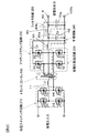
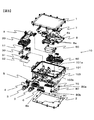
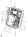
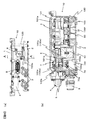
- FIG. 1 is an external perspective view of a DC-DC converter device to which the present invention is applied. It is a figure which shows the main circuit structure of a DC-DC converter apparatus. It is a disassembled perspective view of a DC-DC converter device. It is the perspective view which looked at the inside of a case from the 1st storage room side. It is the perspective view which looked at the inside of a case from the 2nd storage chamber side.
- (A) is the figure which looked at the DC-DC converter apparatus from the side surface in which the output terminal etc. were provided
- (b) is AA arrow sectional drawing of (a).
- FIG. 1 is an external perspective view of a DC-DC converter device 10 according to the present embodiment.
- the DC-DC converter device 10 includes a case 100 as a casing, a top cover 1, and a bottom cover 2.
- a case internal space 100s is formed.
- the case 100 is integrally formed with a GND terminal 100c for connecting a GND terminal for low voltage output.
- the side surface of the case 100 includes a high voltage connector 4 for inputting a high voltage input, a signal connector 5 for inputting / outputting a signal to / from an external electrical component, an output terminal 6 for outputting a low voltage output, and cooling described later.
- a water channel connector 3 that is a refrigerant inlet / outlet of the channel 100f (see FIGS. 5 and 6) is attached.
- the case internal space 100s includes a first storage chamber 101 that opens at an upper opening 101a of the case 100 (see FIG. 4) and a lower opening 102a of the case 100 (see FIG. 5) by a partition wall 100w formed integrally with the case 100. And is divided into a second storage chamber 102 opened at The first storage chamber 101 and the second storage chamber 102 will be described later.
- the case 100 is formed with a cooling flow path 100f through which a refrigerant flows in order to cool the heat generating components in the DC-DC converter device 10 (see FIGS. 5 and 6).
- a refrigerant flows in order to cool the heat generating components in the DC-DC converter device 10 (see FIGS. 5 and 6).
- the cooling flow path 100f is sealed with a seal such as an O-ring 103 (see FIG. 6) so that the refrigerant does not leak from the gap between the case 100 and the bottom cover 2.
- a seal such as an O-ring 103 (see FIG. 6) so that the refrigerant does not leak from the gap between the case 100 and the bottom cover 2.
- a refrigerant in which antifreeze and water are mixed at a ratio of 1: 1 is used.
- the present embodiment is not limited to this, and other refrigerants may be used.
- the above-described cooling structure of the DC-DC converter device 10 is an example, and other cooling structures such as using a cooling
- FIG. 2 is a diagram showing an embodiment of a main circuit configuration of the DC-DC converter device 10.
- the DC-DC converter device 10 includes a high voltage switching circuit 210 composed of an H bridge circuit of MOSFETs (metal oxide field effect transistors) H1 to H4, a low voltage rectifier circuit 220 composed of MOSFETs S1 to S4, and an active clamp circuit 230. It has. Further, the DC-DC converter device 10 includes a transformer T (between a high voltage switching circuit unit (high voltage switching circuit 210) and a low voltage side switching circuit unit (low voltage rectifier circuit 220 and active clamp circuit 230).
- MOSFETs metal oxide field effect transistors
- a main transformer 9) and a resonance coil Lr (resonance coil 11) connected in series on the primary side of the transformer T are provided.
- the high voltage switching circuit 210, the low voltage rectifier circuit 220, and the active clamp circuit 230 are switch-controlled by a control circuit provided on a control circuit board (not shown).
- the low voltage rectifier circuit 220 and the active clamp circuit 230 include MOSFETs S1 and S2 constituting a synchronous rectifier circuit (low voltage rectifier circuit 220) and switching elements S3 and S4 constituting an active clamp circuit.
- the smoothing circuit 240 includes a choke coil L (choke coil 50) and a smoothing capacitor C0 (smoothing capacitor 62).
- a filter circuit 250 including a reactor L2 (reactor 80) and a filter capacitor C2 (filter capacitor 70a) is connected.
- the filter circuit 250 is a circuit that reduces conduction noise output from the output terminal 6.
- FIG. 3 is an exploded perspective view of the DC-DC converter device 10 as an embodiment of the present invention.
- the DC-DC converter device 10 has a case 100 made of metal (for example, made of aluminum die casting).
- case 100 high voltage switching circuit board 20 and MOSFET 31 constituting the above-described high voltage switching circuit part, low voltage rectification circuit board 60 and choke coil 50 constituting the low voltage side switching circuit part, and high voltage switching circuit part are provided.
- the main transformer 9 and the resonance coil 11 connected between the low-voltage side switching circuit section, the reactor 80 and the filter substrate 70 constituting the filter circuit 250, and the connection end 6a of the output terminal 6 are attached.
- a filter capacitor 70a is mounted on the filter substrate 70 (see FIG. 6).
- the MOSFET 31 of the high voltage switching circuit is fixed in close contact with the bottom surface of the case 100 by a leaf spring 30 through an insulating heat radiation sheet 32 having good thermal conductivity, and the terminal of the MOSFET 31 is electrically connected to the high voltage switching circuit board 20 by soldering. Connected to. Thermally conductive grease (not shown) is applied between the bottom surface of the case 100 and the insulating heat dissipation sheet 32 and between the insulating heat dissipation sheet 32 and the MOSFET 31 in order to improve heat transfer.
- the MOSFET 31 that generates heat is cooled by coming into contact with the case 100 having the cooling flow path 100f (see FIGS. 5 and 6) via the insulating heat radiation sheet 32.
- the low-voltage rectifier circuit board 60 employs a metal substrate that forms a circuit pattern on an aluminum plate having high thermal conductivity via an insulating layer.
- the low voltage rectifier circuit board 60 is fixed in close contact with the bottom of the metal case 100.
- Thermally conductive grease (not shown) is applied between the low voltage rectifier circuit board 60 and the bottom surface of the case 100 in order to improve heat transfer.
- the switching elements S1 to S4 that generate heat are cooled by coming into contact with the case 100 having the cooling flow path 100f through the metal substrate of the low-voltage rectifier circuit substrate 60.
- a board frame 8 having a screw boss 8a is attached to the upper part of each component constituting the main circuit described above, and the control board 7 is fixed to the screw boss 8a.
- the board frame 8 is a member that reinforces the control board 7 against vibration shock and plays a role of grounding the control board 7 in terms of circuit. Therefore, the screw boss 8a for fixing the control board 7 is provided at a position where the strength and the circuit are considered.
- the control board 7 is connected to the high voltage switching circuit board 20 and the low voltage rectification circuit board 60 with a signal harness in order to control switching of the high voltage switching circuit 210, the low voltage rectification circuit 220, and the active clamp circuit 230. . Further, the control board 7 is connected to the signal connector 5 by a signal harness for transmission and reception of signals between the DC-DC converter device 10 and external electrical components. In addition to the harness, a flexible wiring board or a direct connector may be used for these connections.
- the case 100 is provided with the first storage chamber 101 and the second storage chamber 102 separated by the partition wall 100w.
- the partition wall 100w includes an isolation wall 100a that horizontally separates the case inner space 100s and a bottom wall 100e that vertically separates the case inner space 100s (see FIGS. 4, 5, and 6).
- the above-described high voltage switching circuit unit, low voltage side switching circuit unit, main transformer 9, resonance coil 11, choke coil 50, control board 7, and board frame 8 are housed in the first housing chamber 101. The By attaching the top cover 1 to the upper opening 101a of the first storage chamber 101, the first storage chamber 101 is sealed.
- the reactor 80 and the filter substrate 70 are stored. Further, a connection end 6 a that is one end of the output terminal 6 is provided in the second storage chamber 102. A connection end 6 b that is the other end of the output terminal 6 protrudes outside the case 100.
- the bottom cover 2 By attaching the bottom cover 2 to the lower opening 102a of the second storage chamber 102, the second storage chamber 102 is sealed. As described above, by attaching the bottom cover 2, the cooling channel 100f is also covered with the lower opening.
- the output terminal 6 is attached from the side surface of the case 100, and the connection end 6 a is connected to the reactor 80 and the filter substrate 70 by the screw 90 in the second storage chamber 102.
- FIG. 4 is a perspective view of the inside of the case 100 as viewed from the first storage chamber 101 side.
- a high voltage switching circuit board 20, a low voltage rectification circuit board 60, a main transformer 9, and a choke coil 50 are disposed in the first storage chamber 101.
- a MOSFET 31 is disposed as shown in FIG.
- a rectifying MOSFET 61 and a rectifying capacitor 62 are mounted on the low voltage rectifier circuit board 60.
- the opening 100d is an opening of a partition wall 100w for connecting the main circuit between the first storage chamber 101 and the second storage chamber 102 of the case 100. Specifically, in the opening 100d, one bus bar 80a of the reactor 80 arranged in the second storage chamber 102 penetrates to the first storage chamber 101 side.
- AC power transformed by the main transformer 9 is rectified to direct current by the low voltage rectifier circuit board 60 and the choke coil 50.
- the rectified electric power is output to one bus bar 80a of the reactor 80 arranged in the second storage chamber.
- One bus bar 80 a of the reactor 80 is connected to the choke coil 50 and the smoothing capacitor 62 in the first storage chamber 101.
- the bottom wall 100e is a surface constituting a bottom wall between the first storage chamber 101 and the second storage chamber of the case 100. That is, the bottom wall 100e is a part of the partition wall 100w that partitions the first storage chamber 101 and the second storage chamber 102.
- a surface of the bottom wall 100e facing the first storage chamber 101 is called a first storage chamber bottom 101e
- a surface facing the second storage chamber 102 is called a second storage chamber bottom 102e (see FIGS. 4 and 6). ).
- the first storage chamber bottom 101e and the second storage chamber bottom 102e face each other.
- a boss 100b is provided on the first storage chamber bottom 101e.
- the boss 100 b plays a role of fixing the control board 7 together with the board frame 8 and grounding the GND of the control board 7 to the case 100.
- FIG. 5 is a perspective view of the inside of the case 100 as viewed from the second storage chamber 102 side.
- a reactor 80 and a capacitor substrate 70 are arranged in the second storage chamber 102.
- the output terminal 6 is attached so as to penetrate from the second storage chamber 102 to the outside of the side surface of the case 100.
- Reactor 80, capacitor substrate 70, and connection end 6a of output terminal 6 are fixed by screws 90 and electrically connected.
- the power rectified by the rectifier circuit on the first storage chamber 101 side is reduced in conduction noise by the reactor 80 and the filter circuit 250 (see FIG. 2) of the capacitor substrate 70, and is output as a low voltage output from the output terminal 6.
- the cooling water channel 100f is a coolant flow channel, and the refrigerant entering from the pipe 3 flows through the cooling water channel 100f, whereby the entire bottom surface of the case 100 is cooled.
- FIG. 6A is a view of the DC-DC converter device 10 as viewed from the side where the output terminal 6 and the like are provided
- FIG. 6B is a cross-sectional view taken along the line AA in FIG. 6A. It is.
- the first storage chamber 101 and the second storage chamber 102 of the case 100 are partitioned by a partition wall 100w, that is, an isolation wall 100a and a bottom wall 100e, and are separated from each other.
- the 1st storage chamber 101 and the 2nd storage chamber 102 are connected only by the opening part 100d mentioned above.
- the low voltage rectifier circuit board 60 and the choke coil 50 which are main circuit components, are disposed in the first storage chamber 101, and the capacitor substrate 70 is disposed in the second storage chamber 102, respectively.
- the board frame 8 is fixed to the case, and the control board 7 is fixed to the board frame 8. A part of the control board 7 is also fixed to the boss 100b provided on the bottom wall 100e of the case 100.
- the control board 7 is connected to the signal connector 5 by a harness or the like (not shown).
- the filter circuit of the reactor 80 and the filter capacitor 70a is connected to the output terminal 6, the noise propagates to the filter capacitor 70a.
- the noise is conducted to the output voltage from the output terminal 6.
- the rectifier circuit board 60, the choke coil 50, the main transformer, and the high voltage switching circuit, which are noise generation sources, are arranged in the first storage chamber.
- the reactor 80, the capacitor substrate 70, and the connection end 6 a of the output terminal 6 are arranged in the second storage chamber 102.
- the first storage chamber 101 is isolated from the second storage chamber 102 by the partition wall 100w. Therefore, noise propagation from the noise generation source to the capacitor substrate 70 can be suppressed. Thereby, it is possible to supply a DC-DC converter device in which conduction noise to the output terminal 6 is suppressed.
- the high voltage switching circuit board 20, the low voltage rectification circuit board 60, the main transformer 9, and the choke coil 50 are arranged in the first storage chamber 101, but the noise is generated most. Only the high voltage switching circuit board 20 may be disposed in the first storage chamber 101. In this case, the conductive noise can be further suppressed by further disposing the main transformer 9 in the first storage chamber 101 as in the present embodiment. Further, by disposing the choke coil 50 in the first storage chamber 101 as in the present embodiment, conduction noise can be further suppressed, and the choke coil 50 is further stored in the first storage as in the present embodiment. By arranging in the chamber 101, conduction noise can be further suppressed, and further, by arranging the smoothing capacitor 62 in the first storage chamber 101, conduction noise can be further suppressed.
- connection end 6 a of the reactor 80, the capacitor substrate 70, and the output terminal 6 is disposed in the second storage chamber 102, but only the connection end 6 a of the capacitor substrate 70 and the output terminal 6 is disposed in the second storage chamber 102. You may do it. In this case, the conductive noise can be further suppressed by disposing the reactor 80 in the second storage chamber 102 as in the present embodiment.
- the noise propagates to the control board 7 and is conducted from the signal connector connected to the control board 7 to the outside.
- noise can be suppressed by providing an LC or CR filter or the like on the control board 7, if noise propagates to the GND pattern on the control board 7, the noise cannot be effectively suppressed by the filter. Therefore, in this embodiment, the distance between the bottom wall 100e and the control board 7 is configured to be short, and the height of the boss 100b provided on the bottom wall 100e is configured to be short. Then, by fixing the GND pattern of the control board 7 to the boss 100b and grounding the GND, the case 100 can be grounded with low impedance. Thereby, it is possible to supply a DC-DC converter device in which noise superimposed on the signal connector 5 connected to the control board 7 is suppressed.
- the present invention is not limited to the above-described embodiment, and includes a transformer for converting a voltage, a switching circuit connected to the primary side of the transformer, and a rectifier circuit connected to the secondary side of the transformer.
- a filter circuit having a reactor and a capacitor connected to the rectifier circuit, a transformer, a switching circuit, a rectifier circuit, a case for housing the filter circuit, an upper plate covering the upper opening of the case, and a lower portion of the case
- a lower plate covering the opening and an output terminal having one end connected to the filter circuit are provided, and a case inner space is formed by the case, the upper plate, and the lower plate, and the case inner space is opened at the upper opening by the partition wall.
- the first storage chamber is divided into a second storage chamber that opens at the lower opening, the partition wall is formed integrally with the case, and the switching circuit and the rectifier circuit are provided in the first storage chamber.
- the capacitor and the output terminal of the filter circuit is intended to include a DC-DC converter devices for various structures, characterized in that arranged in the second housing chamber.
Landscapes
- Engineering & Computer Science (AREA)
- Microelectronics & Electronic Packaging (AREA)
- Power Engineering (AREA)
- Physics & Mathematics (AREA)
- Electromagnetism (AREA)
- Dc-Dc Converters (AREA)
Abstract
出力端子への伝導ノイズを効果的に抑制できるDC-DCコンバータ装置を提供する。 ケースと一体に形成された隔壁によって、ケース内空間を上部開口で開口する第1収納室と、下部開口で開口する第2収納室とに区画し、スイッチング回路および整流回路を第1収納室に配置し、フィルタ回路のコンデンサおよび出力端子を第2収納室に配置した。
Description
本発明は、DC-DCコンバータ装置に関する。
ハイブリッド車やプラグインハイブリッド車、電気自動車などの車両には、動力駆動用の高電圧蓄電池、高電圧蓄電池から電力変換してモータを駆動するためのインバータ装置、高電圧蓄電池から車両のライトやラジオなどの低電圧負荷への電力変換を行うDC-DCコンバータ装置、および低電圧蓄電池が搭載されている。
DC-DCコンバータ装置は、高電圧の直流電圧を交流電圧に変換する高電圧スイッチング回路、交流高電圧を絶縁して交流低電圧に変換するトランス、低電圧交流電圧を直流電圧に変換する低電圧整流回路、および、電圧変換された電圧を出力する出力端子を備えている。低電圧整流回路には、直流出力電圧を平滑にするためのチョークコイルと平滑コンデンサ素子とが設けられている。また、DC-DCコンバータ装置には、出力端子から出力される伝導ノイズを低減するため、リアクトルとコンデンサによるフィルタ回路が設けられている。
しかし、ノイズ源となる高電圧スイッチング回路部品と、伝導ノイズを低減するフィルタ回路および出力端子とを同一の筐体内に収納した実装構造では、装置内でノイズ成分がフィルタ回路や出力端子に伝搬し、十分なノイズ低減効果を得られない。そこで、装置内でのノイズ伝搬の影響を低減するために、従来のDC-DCコンバータ装置では、フィルタ回路の周辺に金属板によるシールドが用いられている(たとえば、特許文献1参照)。
上記特許文献に記載のDC-DCコンバータ装置は、リアクトルおよびコンデンサを有するフィルタ回路部と、隣接するノイズ源との間に、フィルタ回路の導体配線部と絶縁を保ちつつ一体に成形されたシールド板を備え、ノイズ源とフィルタ回路間の放射ノイズを遮断するように構成されている。しかし、上記特許文献に記載のDC-DCコンバータ装置では、シールド板の上方には開口部があり、その開口部にカバーを取り付けることで、ある程度ノイズを遮断しているが、不完全であった。
本発明によるDC-DCコンバータ装置は、電圧を変換するトランスと、トランスの一次側に接続されたスイッチング回路と、トランスの二次側に接続された整流回路と、整流回路に接続されたリアクトルとコンデンサとを有するフィルタ回路と、トランスと、スイッチング回路と、整流回路と、フィルタ回路とを収納するケースと、ケースの上部開口を覆う上板と、ケースの下部開口を覆う下板と、一端がフィルタ回路に接続された出力端子とを備え、ケースと上板と下板とによってケース内空間が形成され、ケース内空間は、隔壁によって、上部開口で開口する第1収納室と、下部開口で開口する第2収納室とに区画され、隔壁は、ケースと一体に形成されており、スイッチング回路および整流回路は、第1収納室に配置され、フィルタ回路のコンデンサおよび出力端子は、第2収納室に配置されることを特徴とする。
本発明によれば、出力端子への伝導ノイズを効果的に抑制できる。
[DC-DCコンバータ装置]
以下、図面を参照して、本発明によるDC-DCコンバータ装置の一実施の形態について説明する。図1は、本実施の形態のDC-DCコンバータ装置10の外観斜視図である。DC-DCコンバータ装置10は、筐体としてのケース100と、トップカバー1と、ボトムカバー2とを備えており、ケース100と、上板であるトップカバー1と、下板であるボトムカバー2とによってケース内空間100sが形成されている。説明の便宜上、図1におけるトップカバー1の上面に垂直な方向を上下方向、または縦方向と呼び、トップカバー1の上面と平行な方向を横方向と呼ぶ。
以下、図面を参照して、本発明によるDC-DCコンバータ装置の一実施の形態について説明する。図1は、本実施の形態のDC-DCコンバータ装置10の外観斜視図である。DC-DCコンバータ装置10は、筐体としてのケース100と、トップカバー1と、ボトムカバー2とを備えており、ケース100と、上板であるトップカバー1と、下板であるボトムカバー2とによってケース内空間100sが形成されている。説明の便宜上、図1におけるトップカバー1の上面に垂直な方向を上下方向、または縦方向と呼び、トップカバー1の上面と平行な方向を横方向と呼ぶ。
ケース100には、低電圧出力のGND側端子を接続するGND端子100cが一体成形されている。ケース100の側面には、高電圧入力を入力する高電圧コネクタ4、外部電装品との間で信号などを入出力する信号コネクタ5、低電圧出力を出力する出力端子6、および、後述する冷却流路100f(図5,6参照)の冷媒の出入り口である水路コネクタ3が取り付けられている。
ケース内空間100sは、ケース100と一体に形成された隔壁100wによって、ケース100の上部開口101a(図4参照)で開口する第1収納室101と、ケース100の下部開口102a(図5参照)で開口する第2収納室102とに区画されている。第1収納室101および第2収納室102については後述する。
ケース100には、DC-DCコンバータ装置10内の発熱部品の冷却のため、冷媒が流れる冷却流路100fが形成されている(図5,6参照)。冷却水路100fは、ケース100の図1における下方の開口がボトムカバー2で覆われている。なお、冷却流路100fは、ケース100とボトムカバー2との隙間から冷媒が漏れ出ないように、Oリング103(図6参照)などのシールで密閉される。本実施の形態では、たとえば、冷媒としては不凍液と水を1:1で混合したものが用いられるが、本実施の形態はこれに限定されるものではなく、他の冷媒を用いてもよい。また、上述したDC-DCコンバータ装置10の冷却構造は一例であり、たとえば空気等の冷却気体を用いるなど、他の冷却構造であってもよい。
[DC-DCコンバータ装置10の主回路構成]
図2はDC-DCコンバータ装置10の主回路構成の一実施の形態を示す図である。DC-DCコンバータ装置10は、MOSFET(金属酸化膜電界効果トランジスタ)H1~H4のHブリッジ回路からなる高電圧スイッチング回路210と、MOSFET S1~S4からなる低電圧整流回路220およびアクティブクランプ回路230とを備えている。また、DC-DCコンバータ装置10は、高電圧スイッチング回路部(高電圧スイッチング回路210)と低圧側スイッチング回路部(低電圧整流回路220およびアクティブクランプ回路230)との間に設けられたトランスT(主トランス9)と、トランスTの一次側に直列に接続された共振コイルLr(共振コイル11)とを備えている。高電圧スイッチング回路210と低電圧整流回路220とアクティブクランプ回路230は、制御回路基板(図示せず)に設けた制御回路によりスイッチ制御が行われる。
図2はDC-DCコンバータ装置10の主回路構成の一実施の形態を示す図である。DC-DCコンバータ装置10は、MOSFET(金属酸化膜電界効果トランジスタ)H1~H4のHブリッジ回路からなる高電圧スイッチング回路210と、MOSFET S1~S4からなる低電圧整流回路220およびアクティブクランプ回路230とを備えている。また、DC-DCコンバータ装置10は、高電圧スイッチング回路部(高電圧スイッチング回路210)と低圧側スイッチング回路部(低電圧整流回路220およびアクティブクランプ回路230)との間に設けられたトランスT(主トランス9)と、トランスTの一次側に直列に接続された共振コイルLr(共振コイル11)とを備えている。高電圧スイッチング回路210と低電圧整流回路220とアクティブクランプ回路230は、制御回路基板(図示せず)に設けた制御回路によりスイッチ制御が行われる。
低電圧整流回路220とアクティブクランプ回路230は、同期整流回路(低電圧整流回路220)を構成するMOSFET S1,S2と、アクティブクランプ回路を構成するスイッチング素子S3,S4とを備える。平滑回路240は、チョークコイルL(チョークコイル50)と平滑コンデンサC0(平滑コンデンサ62)とを備える。
平滑回路240と出力端子6の間には、リアクトルL2(リアクトル80)とフィルタコンデンサC2(フィルタコンデンサ70a)とによるフィルタ回路250が接続されている。フィルタ回路250は、出力端子6から出力される伝導ノイズを低減する回路である。
[DC-DCコンバータ装置10の構造]
図3は、本発明の一実施の形態としてのDC-DCコンバータ装置10の分解斜視図である。DC-DCコンバータ装置10は、金属製(例えば、アルミダイカスト製)のケース100を有する。ケース100内には、上述した高電圧スイッチング回路部を構成する高電圧スイッチング回路基板20とMOSFET31、低圧側スイッチング回路部を構成する低電圧整流回路基板60とチョークコイル50、高電圧スイッチング回路部と低圧側スイッチング回路部との間に接続される主トランス9と共振コイル11、フィルタ回路250を構成するリアクトル80とフィルタ基板70、出力端子6の接続端6aが取付けられている。なお、フィルタ基板70には、フィルタコンデンサ70aが搭載されている(図6参照)。
図3は、本発明の一実施の形態としてのDC-DCコンバータ装置10の分解斜視図である。DC-DCコンバータ装置10は、金属製(例えば、アルミダイカスト製)のケース100を有する。ケース100内には、上述した高電圧スイッチング回路部を構成する高電圧スイッチング回路基板20とMOSFET31、低圧側スイッチング回路部を構成する低電圧整流回路基板60とチョークコイル50、高電圧スイッチング回路部と低圧側スイッチング回路部との間に接続される主トランス9と共振コイル11、フィルタ回路250を構成するリアクトル80とフィルタ基板70、出力端子6の接続端6aが取付けられている。なお、フィルタ基板70には、フィルタコンデンサ70aが搭載されている(図6参照)。
高電圧スイッチング回路のMOSFET31は、熱伝導性の良い絶縁放熱シート32を介し、板ばね30でケース100の底面に密着して固定され、MOSFET31の端子が高電圧スイッチング回路基板20と半田で電気的に接続される。ケース100の底面と絶縁放熱シート32の間、および、絶縁放熱シート32とMOSFET31の間には熱伝達を向上するために、熱伝導性グリース(図示せず)が塗布されている。発熱するMOSFET31は絶縁放熱シート32を介して冷却流路100f(図5,6参照)を持つケース100に接触することで冷却される。
低電圧整流回路基板60には、図2の低電圧整流回路220のスイッチング素子S1,S2と、アクティブクランプ回路230のスイッチング素子S3,S4と、平滑コンデンサ62が搭載されている。本実施の形態では、低電圧整流回路基板60には、熱伝導率の高いアルミ板に絶縁層を介して回路パターンを構成する金属基板を採用している。低電圧整流回路基板60は金属製のケース100の底部に密着して固定されている。低電圧整流回路基板60とケース100の底面との間には、熱伝達を向上するために、熱伝導性グリース(図示せず)が塗布されている。発熱するスイッチング素子S1~S4は、低電圧整流回路基板60の金属基板を介して冷却流路100fを持つケース100に接触することで冷却される。
上述した主回路を構成する各部品の上部には、ねじボス8aを有する基板フレーム8が取付けられ、そのねじボス8aに制御基板7が固定されている。基板フレーム8は、振動衝撃に対して制御基板7を補強する役割と、回路的に制御基板7のGND接地を取る役割を果たす部材である。そのため、制御基板7を固定するねじボス8aは、強度と、回路的に考慮された位置に設けられている。
制御基板7は、高電圧スイッチング回路210と低電圧整流回路220とアクティブクランプ回路230とのスイッチングを制御するため、高電圧スイッチング回路基板20および低電圧整流回路基板60と信号ハーネスで接続されている。また、DC―DCコンバータ装置10と外部の電装品との信号の送受信のため、制御基板7は信号コネクタ5と信号ハーネスで接続されている。これらの接続にはハーネス以外にも、フレキシブル配線板や、ダイレクトコネクタを用いても良い。
上述したように、ケース100には、隔壁100wで隔てられた第1収納室101と第2収納室102とが設けられている。なお、隔壁100wは、ケース内空間100sを横方向に隔てる隔離壁100aと、ケース内空間100sを縦方向に隔てる底壁100eとを有する(図4,5,6参照)。本実施の形態では、上述の高電圧スイッチング回路部、低圧側スイッチング回路部、主トランス9、共振コイル11、チョークコイル50、制御基板7、および、基板フレーム8が第1収納室101に収納される。第1収納室101の上部開口部101aにトップカバー1が取付けられることで、第1収納室101が密閉される。
第2収納室102には、リアクトル80とフィルタ基板70が収納される。また、出力端子6の一方の端部である接続端6aが第2収納室102の内部に設けられる。なお、出力端子6の他方の端部である接続端6bは、ケース100の外部に突出している。第2収納室102の下部開口部102aにボトムカバー2が取付けられることで、第2収納室102が密閉される。なお、上述したように、ボトムカバー2が取付けられることで、冷却流路100fも下方の開口が覆われる。出力端子6は、ケース100の側面から取付けられており、第2収納室102内で、接続端6aがねじ90によってリアクトル80およびフィルタ基板70と接続される。
図4は、ケース100の内部を第1収納室101側から見た斜視図である。第1収納室101には、高電圧スイッチング回路基板20と、低電圧整流回路基板60と、主トランス9と、チョークコイル50とが配置されている。高電圧スイッチング回路基板20の下部には図4では図示されていないが、図3に示すようにMOSFET31が配置されている。低電圧整流回路基板60には、整流用MOSFET61、整流コンデンサ62が搭載されている。また、開口部100dは、ケース100の第1収納室101と第2収納室102の間で主回路を繋ぐための隔壁100wの開口部である。具体的には、開口部100dでは、第2収納室102に配置されているリアクトル80の一方のブスバー80aが第1収納室101側へ貫通している。
主トランス9で変圧された交流電力は、低電圧整流回路基板60とチョークコイル50で直流に整流される。整流された電力は、第2収納室に配置されているリアクトル80の一方のバスバー80aへ出力される。なお、リアクトル80の一方のバスバー80aは、第1収納室101内で、チョークコイル50および平滑コンデンサ62と接続されている。
底壁100eは、ケース100の第1収納室101と第2収納室の間の底壁を構成する面である。すなわち、底壁100eは、第1収納室101と第2収納室102とを区画する隔壁100wの一部である。底壁100eで、第1収納室101側に向いた面を第1収納室底部101eと呼び、第2収納室102側に向いた面を第2収納室底部102eと呼ぶ(図4,6参照)。第1収納室底部101eと第2収納室底部102eとは互いに対向している。第1収納室底部101e上には、ボス100bが設けられている。ボス100bは、基板フレーム8とともに制御基板7の固定、および、制御基板7のGNDをケース100に接地させる役割を果たす。
図5は、ケース100の内部を第2収納室102側から見た斜視図である。第2収納室102には、リアクトル80と、コンデンサ基板70とが配置されている。出力端子6は、第2収納室102からケース100の側面外側に貫通して取り付けられている。リアクトル80と、コンデンサ基板70と、出力端子6の接続端6aとは、ねじ90で固定されて電気的に接続されている。第1収納室101側の整流回路で整流された電力は、リアクトル80と、コンデンサ基板70のフィルタ回路250(図2参照)により伝導ノイズが低減されて、出力端子6から低電圧出力として出力される。
上述したように、冷却水路100fは冷媒の流水路であり、パイプ3から入った冷媒が、冷却水路100fを流れることで、ケース100の底面全体が冷却される。
図6(a)は、DC-DCコンバータ装置10を出力端子6等が設けられた側面から見た図であり、図6(b)は、図6(a)のA-A矢視断面図である。図6(b)に示すように、ケース100の第1収納室101と第2収納室102とは、隔壁100w、すなわち、隔離壁100aおよび底壁100eによって区画されて、互いに隔てられている。なお、上述したリアクトル80の一方のブスバー80aを通すため、第1収納室101と第2収納室102とは上述した開口部100dのみで繋がっている。
上述したように、主回路部品の低電圧整流回路基板60とチョークコイル50は第1収納室101、コンデンサ基板70は第2収納室102にそれぞれ配置されている。整流回路基板60とチョークコイル50の図6における図示上方では、基板フレーム8がケースに固定され、制御基板7が基板フレーム8に固定されている。また、ケース100の底壁100eに設けられたボス100bにも制御基板7の一部が固定されている。制御基板7は、信号コネクタ5とハーネス等(図示せず)で接続されている。
コンデンサのインピーダンスが低いため、装置内のノイズがコンデンサを介して伝搬し易く、出力端子6にリアクトル80とフィルタコンデンサ70aのフィルタ回路を接続しても、フィルタコンデンサ70aにノイズが伝搬することにより、そのノイズが出力端子6からの出力電圧に伝導してしまう。本実施の形態では、ノイズの発生源である整流回路基板60と、チョークコイル50と、主トランスと、高電圧スイッチング回路とを第1収納室に配置した。そして、第2収納室102にリアクトル80とコンデンサ基板70と出力端子6の接続端6aを配置した。上述したように、第1収納室101は、隔壁100wにより第2収納室102と空間が遮断されている。そのため、ノイズの発生源からコンデンサ基板70へのノイズ伝搬を抑制できる。これにより、出力端子6への伝導ノイズを抑制したDC-DCコンバータ装置を供給することができる。
本実施の形態では、第1収納室101に、高電圧スイッチング回路基板20と、低電圧整流回路基板60と、主トランス9と、チョークコイル50とを配置しているが、最もノイズを発生する高電圧スイッチング回路基板20のみを第1収納室101に配置しても良い。この場合、本実施の形態のように、さらに主トランス9を第1収納室101に配置することで、伝導ノイズを抑制さらに抑制できる。また、本実施の形態のように、さらにチョークコイル50を第1収納室101に配置することで、伝導ノイズを抑制さらに抑制でき、本実施の形態のように、さらにチョークコイル50を第1収納室101に配置することで、伝導ノイズを抑制さらに抑制でき、さらに平滑コンデンサ62を第1収納室101に配置することで、伝導ノイズを抑制さらに抑制できる。
一方、第2収納室102に、リアクトル80とコンデンサ基板70と出力端子6の接続端6aを配置しているが、コンデンサ基板70と出力端子6の接続端6aのみを第2収納室102に配置しても良い。この場合、本実施の形態のように、さらにリアクトル80を第2収納室102に配置することで、伝導ノイズを抑制さらに抑制できる。
一方、ノイズは、制御基板7にも伝搬し、制御基板7に接続された信号コネクタから外部へ伝導してしまう。制御基板7にLC、またはCRフィルタなどを設けてノイズを抑制することができるが、制御基板7上のGNDパターンにノイズが伝搬すると、フィルタによってノイズを効果的に抑制できない。そこで、本実施の形態では、底壁100eと制御基板7との距離が短くなるように構成し、底壁100eの上に設けられたボス100bの高さが短くなるように構成した。そして、制御基板7のGNDパターンをボス100bに固定してGND接地する事により、ケース100に対して低インピーダンスで接地する事ができる。これにより、制御基板7に接続される信号コネクタ5に重畳するノイズを抑制したDC-DCコンバータ装置を供給することができる。
なお、上述した実施の形態および変形例は、それぞれ組み合わせてもよい。
なお、本発明は、上述した実施の形態のものに何ら限定されず、電圧を変換するトランスと、トランスの一次側に接続されたスイッチング回路と、トランスの二次側に接続された整流回路と、整流回路に接続されたリアクトルとコンデンサとを有するフィルタ回路と、トランスと、スイッチング回路と、整流回路と、フィルタ回路とを収納するケースと、ケースの上部開口を覆う上板と、ケースの下部開口を覆う下板と、一端がフィルタ回路に接続された出力端子とを備え、ケースと上板と下板とによってケース内空間が形成され、ケース内空間は、隔壁によって、上部開口で開口する第1収納室と、下部開口で開口する第2収納室とに区画され、隔壁は、ケースと一体に形成されており、スイッチング回路および整流回路は、第1収納室に配置され、フィルタ回路のコンデンサおよび出力端子は、第2収納室に配置されることを特徴とする各種構造のDC-DCコンバータ装置を含むものである。
1 トップカバー、2 ボトムカバー、4 高電圧コネクタ、6 出力端子、7 制御基板、8 基板フレーム、9 主トランス(トランスT)、10 DC-DCコンバータ装置、11 共振コイル(共振コイルLr)、50 チョークコイル(チョークコイルL)、60 低電圧整流回路基板、62 平滑コンデンサ(平滑コンデンサC0)、70 フィルタ基板、70a フィルタコンデンサ(フィルタコンデンサC2)、80 リアクトル(リアクトルL2)、100 ケース、100a 隔離壁、100b ボス、100c GND端子、100e 底壁、100s ケース内空間、100w 隔壁、101 第1収納室、101e 第1収納室底部、102 第2収納室、210 高電圧スイッチング回路、220 低電圧整流回路、230 アクティブクランプ回路、240 平滑回路、250 フィルタ回路
Claims (6)
- 電圧を変換するトランスと、
前記トランスの一次側に接続されたスイッチング回路と、
前記トランスの二次側に接続された整流回路と、
前記整流回路に接続されたリアクトルとコンデンサとを有するフィルタ回路と、
前記トランスと、前記スイッチング回路と、前記整流回路と、前記フィルタ回路とを収納するケースと、
前記ケースの上部開口を覆う上板と、
前記ケースの下部開口を覆う下板と、
一端が前記フィルタ回路に接続された出力端子とを備え、
前記ケースと前記上板と前記下板とによってケース内空間が形成され、
前記ケース内空間は、隔壁によって、前記上部開口で開口する第1収納室と、前記下部開口で開口する第2収納室とに区画され、
前記隔壁は、前記ケースと一体に形成されており、
前記スイッチング回路および前記整流回路は、前記第1収納室に配置され、
前記フィルタ回路の前記コンデンサおよび前記出力端子は、前記第2収納室に配置されることを特徴とするDC-DCコンバータ装置。 - 請求項1に記載のDC-DCコンバータ装置において、
前記トランスは、前記第1収納室に配置されることを特徴とするDC-DCコンバータ装置。 - 請求項1または請求項2に記載のDC-DCコンバータ装置において、
前記フィルタ回路の前記リアクトルは、前記第2収納室に配置されることを特徴とするDC-DCコンバータ装置。 - 請求項3に記載のDC-DCコンバータ装置において、
前記整流回路は、チョークコイルと平滑コンデンサとを有する平滑回路を備え、
前記平滑回路の前記チョークコイルは、前記第1収納室に配置されることを特徴とするDC-DCコンバータ装置。 - 請求項4に記載のDC-DCコンバータ装置において、
前記平滑回路の前記平滑コンデンサは、前記第1収納室に配置されることを特徴とするDC-DCコンバータ装置。 - 請求項1に記載のDC-DCコンバータ装置において、
前記スイッチング回路と前記整流回路とを制御する制御回路をさらに備え、
前記ケースの前記第1収納室の底部のうち、前記第2収納室の底部と対向する部位に固定ボスが設けられ、
前記制御回路のグランドは、前記固定ボスに接地されていることを特徴とするDC-DCコンバータ装置。
Priority Applications (1)
| Application Number | Priority Date | Filing Date | Title |
|---|---|---|---|
| JP2015532736A JP6186439B2 (ja) | 2013-08-23 | 2014-05-28 | Dc−dcコンバータ装置 |
Applications Claiming Priority (2)
| Application Number | Priority Date | Filing Date | Title |
|---|---|---|---|
| JP2013-173329 | 2013-08-23 | ||
| JP2013173329 | 2013-08-23 |
Publications (1)
| Publication Number | Publication Date |
|---|---|
| WO2015025581A1 true WO2015025581A1 (ja) | 2015-02-26 |
Family
ID=52483366
Family Applications (1)
| Application Number | Title | Priority Date | Filing Date |
|---|---|---|---|
| PCT/JP2014/064051 Ceased WO2015025581A1 (ja) | 2013-08-23 | 2014-05-28 | Dc-dcコンバータ装置 |
Country Status (2)
| Country | Link |
|---|---|
| JP (1) | JP6186439B2 (ja) |
| WO (1) | WO2015025581A1 (ja) |
Cited By (1)
| Publication number | Priority date | Publication date | Assignee | Title |
|---|---|---|---|---|
| EP2960509A1 (en) * | 2014-05-23 | 2015-12-30 | Valeo Japan Co., Ltd. | Current conversion device for an electrical machine, notably a drive motor of a compressor |
Citations (4)
| Publication number | Priority date | Publication date | Assignee | Title |
|---|---|---|---|---|
| JP2001044685A (ja) * | 1999-07-30 | 2001-02-16 | Toyota Autom Loom Works Ltd | ノイズフィルタ装置 |
| JP2001217577A (ja) * | 2000-11-20 | 2001-08-10 | Hitachi Ltd | 電気装置 |
| JP2010004114A (ja) * | 2008-06-18 | 2010-01-07 | Toshiba Corp | 高周波モジュール |
| JP2013034273A (ja) * | 2011-08-01 | 2013-02-14 | Denso Corp | 電源装置 |
-
2014
- 2014-05-28 JP JP2015532736A patent/JP6186439B2/ja active Active
- 2014-05-28 WO PCT/JP2014/064051 patent/WO2015025581A1/ja not_active Ceased
Patent Citations (4)
| Publication number | Priority date | Publication date | Assignee | Title |
|---|---|---|---|---|
| JP2001044685A (ja) * | 1999-07-30 | 2001-02-16 | Toyota Autom Loom Works Ltd | ノイズフィルタ装置 |
| JP2001217577A (ja) * | 2000-11-20 | 2001-08-10 | Hitachi Ltd | 電気装置 |
| JP2010004114A (ja) * | 2008-06-18 | 2010-01-07 | Toshiba Corp | 高周波モジュール |
| JP2013034273A (ja) * | 2011-08-01 | 2013-02-14 | Denso Corp | 電源装置 |
Cited By (1)
| Publication number | Priority date | Publication date | Assignee | Title |
|---|---|---|---|---|
| EP2960509A1 (en) * | 2014-05-23 | 2015-12-30 | Valeo Japan Co., Ltd. | Current conversion device for an electrical machine, notably a drive motor of a compressor |
Also Published As
| Publication number | Publication date |
|---|---|
| JP6186439B2 (ja) | 2017-08-23 |
| JPWO2015025581A1 (ja) | 2017-03-02 |
Similar Documents
| Publication | Publication Date | Title |
|---|---|---|
| US10128770B2 (en) | Converter and electric power conversion apparatus | |
| JP5743851B2 (ja) | 電子装置 | |
| US9866127B2 (en) | Electrical power converting device | |
| JP6214710B2 (ja) | 電力変換装置 | |
| US9776514B2 (en) | DC-DC converter | |
| JP6104347B1 (ja) | 電力変換装置 | |
| JP6169181B2 (ja) | Dc−dcコンバータ装置 | |
| JP6012330B2 (ja) | Dcdcコンバータ | |
| JP5914290B2 (ja) | 電力変換装置 | |
| US9814154B2 (en) | Power converter | |
| JP5818754B2 (ja) | Dc−dcコンバータ装置 | |
| US20150163961A1 (en) | Power Conversion Apparatus | |
| JP2013034273A (ja) | 電源装置 | |
| JP6186439B2 (ja) | Dc−dcコンバータ装置 | |
| JP2016036219A (ja) | Dc−dcコンバータ | |
| JP6851999B2 (ja) | 電力変換装置 | |
| JP5958493B2 (ja) | 電源装置 | |
| CN111313656B (zh) | 电源装置 | |
| JP2013034272A (ja) | 電源装置 |
Legal Events
| Date | Code | Title | Description |
|---|---|---|---|
| 121 | Ep: the epo has been informed by wipo that ep was designated in this application |
Ref document number: 14838109 Country of ref document: EP Kind code of ref document: A1 |
|
| ENP | Entry into the national phase |
Ref document number: 2015532736 Country of ref document: JP Kind code of ref document: A |
|
| NENP | Non-entry into the national phase |
Ref country code: DE |
|
| 122 | Ep: pct application non-entry in european phase |
Ref document number: 14838109 Country of ref document: EP Kind code of ref document: A1 |