WO2015022892A1 - 光学フィルターおよび前記フィルターを用いた装置 - Google Patents
光学フィルターおよび前記フィルターを用いた装置 Download PDFInfo
- Publication number
- WO2015022892A1 WO2015022892A1 PCT/JP2014/070706 JP2014070706W WO2015022892A1 WO 2015022892 A1 WO2015022892 A1 WO 2015022892A1 JP 2014070706 W JP2014070706 W JP 2014070706W WO 2015022892 A1 WO2015022892 A1 WO 2015022892A1
- Authority
- WO
- WIPO (PCT)
- Prior art keywords
- group
- resin
- optical filter
- carbon atoms
- infrared
- Prior art date
- Legal status (The legal status is an assumption and is not a legal conclusion. Google has not performed a legal analysis and makes no representation as to the accuracy of the status listed.)
- Ceased
Links
Images

Classifications
-
- G—PHYSICS
- G02—OPTICS
- G02B—OPTICAL ELEMENTS, SYSTEMS OR APPARATUS
- G02B5/00—Optical elements other than lenses
- G02B5/20—Filters
- G02B5/22—Absorbing filters
- G02B5/223—Absorbing filters containing organic substances, e.g. dyes, inks or pigments
-
- G—PHYSICS
- G02—OPTICS
- G02B—OPTICAL ELEMENTS, SYSTEMS OR APPARATUS
- G02B5/00—Optical elements other than lenses
- G02B5/20—Filters
- G02B5/208—Filters for use with infrared or ultraviolet radiation, e.g. for separating visible light from infrared and/or ultraviolet radiation
-
- G—PHYSICS
- G02—OPTICS
- G02B—OPTICAL ELEMENTS, SYSTEMS OR APPARATUS
- G02B5/00—Optical elements other than lenses
- G02B5/20—Filters
- G02B5/28—Interference filters
- G02B5/281—Interference filters designed for the infrared light
- G02B5/282—Interference filters designed for the infrared light reflecting for infrared and transparent for visible light, e.g. heat reflectors, laser protection
Definitions
- the present invention relates to an optical filter and an apparatus using the filter.
- a solid-state imaging device such as a video camera, a digital still camera, a mobile phone with a camera function, a CCD or CMOS image sensor, which is a solid-state imaging device for color images.
- These solid-state imaging devices use a silicon photodiode having sensitivity to near infrared rays in the light receiving portion.
- These solid-state image sensors need to perform visibility correction to make them look natural when viewed by the human eye, and are optical filters that selectively transmit or cut light in a specific wavelength region (for example, near-infrared cut) Filter) is often used.
- Patent Document 1 describes a near-infrared cut filter using a substrate made of a transparent resin and containing a near-infrared absorbing dye in the transparent resin.
- the near-infrared cut filter described in Patent Document 1 may not always have sufficient near-infrared absorption characteristics.
- the present applicant has proposed a near-infrared cut filter having a norbornene-based resin substrate and a near-infrared reflective film in Patent Document 2.
- the near-infrared cut filter described in Patent Document 2 is excellent in near-infrared cut characteristics, moisture absorption resistance and impact resistance, but cannot take a wide viewing angle.
- Patent Document 3 proposes a near-infrared cut filter having a wide viewing angle and a high visible light transmittance.
- the image quality level required for camera images has become very high even in mobile devices and the like, and it is desired to suppress the generation of ghost light.
- the optical filter in addition to high visible light transmittance, a wide range of wavelengths from 800 to 1200 nm. In the infrared region, a high light cut characteristic is required even for a light beam having a high incident angle. Conventional optical filters cannot satisfy such characteristics in a well-balanced manner. This invention makes it a subject to provide the optical filter which has the said light cut characteristic.
- An optical filter having a transparent resin substrate and a near-infrared reflective film formed on at least one surface of the substrate and satisfying the following requirements (A) to (B): (A) In the wavelength range of 430 to 580 nm, the average value of the transmittance when measured from the vertical direction of the optical filter is 75% or more.
- the transparent resin constituting the transparent resin substrate is a cyclic olefin resin, aromatic polyether resin, polyimide resin, fluorene polycarbonate resin, fluorene polyester resin, polycarbonate resin, polyamide resin, poly Allylate resin, polysulfone resin, polyethersulfone resin, polyparaphenylene resin, polyamideimide resin, polyethylene naphthalate resin, fluorinated aromatic polymer resin, (modified) acrylic resin, epoxy resin
- the optical filter according to [1] which is at least one resin selected from the group consisting of an allyl ester resin and a silsesquioxane resin.
- the transparent resin substrate is at least one selected from the group consisting of squarylium compounds, cyanine compounds, phthalocyanine compounds, naphthalocyanine compounds, croconium compounds, dithiol compounds, diimonium compounds, and porphyrin compounds.
- the near-infrared absorbing dye contains at least one selected from the group consisting of a squarylium compound represented by formula (I) described later and a squarylium compound represented by formula (II) described later.
- [6] In the wavelength range of 800 to 1200 nm, the average reflectance when measured from an angle of 45 ° with respect to the vertical direction of the optical filter is 70% when measured from any side of the optical filter.
- the optical filter according to any one of [1] to [7] which is for a solid-state imaging device.
- a solid-state imaging device comprising the optical filter according to any one of [1] to [7].
- a camera module comprising the optical filter according to any one of [1] to [7].
- an optical filter having a high visible light transmittance and a high light-cutting characteristic even for a light having a high incident angle in a wide infrared region having a wavelength of 800 to 1200 nm. Can do.
- an optical filter is used for a solid-state imaging device, a ghost light is not generated and a camera image with good image quality can be obtained even in a small camera module such as a mobile device.
- FIG. 1A is a schematic diagram showing a method for measuring the transmittance when measured from the vertical direction of the optical filter.
- FIG. 1B is a schematic diagram illustrating a method of measuring the reflectance when measured from an angle of 45 ° with respect to the vertical direction of the optical filter.
- FIG. 1C is a schematic diagram illustrating a method of measuring the reflectance when measured from an angle of 5 ° with respect to the vertical direction of the optical filter.
- the optical filter of the present invention has a transparent resin substrate and a near-infrared reflective film formed on at least one surface of the substrate.
- the near-infrared reflective film is provided on both surfaces of the transparent resin substrate, the warp of the optical filter can be further reduced as compared with the case where the near-infrared reflective film is provided only on one side.
- the optical filter of the present invention satisfies the following requirements (A) to (B).
- (A) In a wavelength range of 430 to 580 nm, the average value of transmittance when measured from the vertical direction of the optical filter is 75% or more. This average value is preferably 78% or more, more preferably 80% or more.
- an optical filter having a high transmittance in such a wavelength region of 430 to 580 nm can be obtained by using a transparent resin described later and an absorbent having no absorption maximum wavelength in the wavelength region. it can.
- the vertical direction of the optical filter means a direction perpendicular to the filter surface.
- the average reflectance when measured from one side of the optical filter at an angle of 45 ° with respect to the vertical direction of the optical filter is 70% or more. This average value is preferably 80% or more, more preferably 90% or more.
- the reflectance measured from an angle of 45 ° with respect to the vertical direction of the optical filter is also referred to as “45 ° reflectance”.
- the average value of the 45 ° reflectance measured from one surface side of the optical filter and the average value of the 45 ° reflectance measured from the other surface side are both 70% or more, More preferably, it is 75% or more, More preferably, it is 85% or more.
- the optical filter has a high light-cut characteristic in a wide range of infrared regions, even for light rays with a high incident angle, for example, light rays with an incident angle of about 45 ° with respect to the vertical direction of the filter. Can be realized. Therefore, a wide viewing angle can be ensured, and generation of ghost light in the camera image can be suppressed.
- a near-infrared reflecting film having a high average value of 45 ° reflectance in a wavelength region of 800 to 1200 nm is formed on a transparent resin substrate, so that light in the near-infrared region is effectively cut, and a wavelength of 800
- An optical filter having a sufficiently high 45 ° reflectance can be obtained in the region of ⁇ 1200 nm. Thereby, a ghost can be reduced and the image quality of the obtained camera image improves.
- a high refractive index material, a low refractive index material, each high refractive index material, and a low refractive index material are laminated so as to achieve both an antireflection effect in the visible range and a light cut effect in the near infrared range.
- a near-infrared reflective film in which the order of the thickness, the thickness of each layer, the number of layers, and the like are optimized can be provided on the transparent resin substrate.
- an optical filter having sufficient reflection characteristics can be obtained even in a light beam having an incident angle of 45 ° with respect to the vertical direction of the optical filter in the wavelength region of 800 to 1200 nm.
- optical thin film design software for example, manufactured by Essential Macleod, Thin Film Center
- a dye having absorption in the wavelength range of 800 to 1200 nm in a range that does not adversely affect the transmittance in the visible range in addition to the application of the near-infrared reflective film described above, a dye having absorption in the wavelength range of 800 to 1200 nm in a range that does not adversely affect the transmittance in the visible range.
- metal-containing fine particles and the like can be further added to the transparent resin substrate.
- an optical filter satisfying all of the requirements (A) to (B) in a well-balanced manner can be obtained by using a transparent resin substrate and controlling the properties of the near-infrared reflective film. Since the optical filter of the present invention satisfies all the requirements (A) to (B), a satisfactory high image quality can be obtained particularly when used in a solid-state imaging device application as compared with the conventional optical filter.
- the optical filter of the present invention preferably further satisfies the requirement (C).
- the requirement (B) is satisfied in the optical filter, the requirement (C) is also usually satisfied.
- C) In the wavelength range of 800 to 1200 nm, the average reflectance measured from one surface side of the optical filter at an angle of 5 ° with respect to the vertical direction of the optical filter is 70% or more. This average value is preferably 80% or more, more preferably 90% or more. The reflectance measured from an angle of 5 ° with respect to the vertical direction of the optical filter is also referred to as “5 ° reflectance”.
- the average value of the 5 ° reflectance measured from one surface side of the optical filter and the average value of the 5 ° reflectance measured from the other surface side are both 70% or more. Is preferable, more preferably 80% or more, and still more preferably 90% or more.
- the transparent resin substrate (hereinafter also referred to as “resin substrate”) constituting the optical filter of the present invention preferably contains a transparent resin and a near-infrared absorbing dye, and more preferably has an absorption maximum at a wavelength of 600 to 800 nm. It is in the range. If the absorption maximum wavelength of the substrate is within this range, the substrate can selectively and efficiently cut near infrared rays.
- the resin substrate may be a single layer or multiple layers.
- the thickness of the resin substrate can be appropriately selected according to the desired application, and is not particularly limited, but is preferably 30 to 250 ⁇ m, more preferably 40 to 200 ⁇ m, and particularly preferably 50 to 150 ⁇ m.
- the optical filter using the substrate can be reduced in size and weight, and can be suitably used for various applications such as a solid-state imaging device.
- the filter when the filter is used in a lens unit such as a camera module, the height of the lens unit can be reduced.
- the resin substrate can be formed using a transparent resin.
- the transparent resin is not particularly limited as long as it does not impair the effects of the present invention. For example, it ensures thermal stability and moldability to a film, and dielectrics are formed by high-temperature deposition performed at a deposition temperature of 100 ° C. or higher.
- Tg glass transition temperature
- the glass transition temperature of the resin is 140 ° C. or higher because a film capable of depositing a dielectric multilayer film at a higher temperature can be obtained.
- the total light transmittance (JIS K7105) of the resin plate is preferably 75 to 95%, more preferably 78 to 95. %, Particularly preferably 80 to 95% of the resin can be used. If a resin having a total light transmittance in such a range is used, the resulting substrate exhibits good transparency as an optical film.
- the weight average molecular weight (Mw) in terms of polystyrene measured by a gel permeation chromatography (GPC) method of the transparent resin is usually 15,000 to 350,000, preferably 30,000 to 250,000;
- the average molecular weight (Mn) is usually 10,000 to 150,000, preferably 20,000 to 100,000.
- the transparent resin examples include cyclic olefin resins, aromatic polyether resins, polyimide resins, fluorene polycarbonate resins, fluorene polyester resins, polycarbonate resins, polyamide (aramid) resins, polyarylate resins, polysulfones. Resin, polyethersulfone resin, polyparaphenylene resin, polyamideimide resin, polyethylene naphthalate (PEN) resin, fluorinated aromatic polymer resin, (modified) acrylic resin, epoxy resin, allyl Examples include ester resins and silsesquioxane resins.
- Cyclic olefin-based resin The cyclic olefin-based resin is at least one selected from the group consisting of a monomer represented by the following formula (X 0 ) and a monomer represented by the following formula (Y 0 ). A resin obtained from these monomers and a resin obtained by hydrogenating the resin are preferred.
- R x1 to R x4 each independently represents an atom or group selected from the following (i ′) to (ix ′), and k x , mx and p x are each independently 0 Or represents a positive integer.
- (Ix ′) A monocyclic hydrocarbon ring or heterocycle formed by bonding R x2 and R x3 to each other (provided that R x1 and R x4 not involved in the bonding are each independently the above (i Represents an atom or group selected from ') to (vi').
- R y1 and R y2 each independently represents an atom or group selected from the above (i ′) to (vi ′), or R y1 and R y2 are bonded to each other formed monocyclic or polycyclic alicyclic hydrocarbon, an aromatic hydrocarbon or heterocyclic, k y and p y are each independently 0 or a positive integer.
- Aromatic polyether-based resin is at least one selected from the group consisting of a structural unit represented by the following formula (1) and a structural unit represented by the following formula (2). It preferably has a structural unit.
- R 1 to R 4 each independently represents a monovalent organic group having 1 to 12 carbon atoms, and a to d each independently represent an integer of 0 to 4.
- the aromatic polyether resin further has at least one structural unit selected from the group consisting of a structural unit represented by the following formula (3) and a structural unit represented by the following formula (4). Is preferred.
- R 5 and R 6 each independently represent a monovalent organic group having 1 to 12 carbon atoms
- Z represents a single bond, —O—, —S—, —SO 2 —,> C ⁇ O, —CONH—, —COO— or a divalent organic group having 1 to 12 carbon atoms
- e and f each independently represent an integer of 0 to 4, and n represents 0 or 1.
- R 7 , R 8 , Y, m, g and h are each independently synonymous with R 7 , R 8 , Y, m, g and h in the formula (2), and R 5 , R 6 , Z, n, e and f are independently the same as R 5 , R 6 , Z, n, e and f in the formula (3).
- the polyimide resin is not particularly limited as long as it is a polymer compound containing an imide bond in a repeating unit. For example, it is described in JP-A-2006-199945 and JP-A-2008-163107. It can be synthesized by the method that has been.
- Fluorene polycarbonate resin is not particularly limited as long as it is a polycarbonate resin containing a fluorene moiety, and can be synthesized, for example, by the method described in JP-A-2008-163194. .
- Fluorene polyester-based resin is not particularly limited as long as it is a polyester resin containing a fluorene moiety, and is described in, for example, JP 2010-285505 A or JP 2011-197450 A. Can be synthesized by any method.
- Fluorinated aromatic polymer resin is not particularly limited, but has at least one fluorine-containing aromatic ring, an ether bond, a ketone bond, a sulfone bond, an amide bond, and an imide bond. And a polymer containing a repeating unit containing at least one bond selected from the group consisting of ester bonds, and can be synthesized, for example, by the method described in JP-A-2008-181121.
- Examples of commercially available transparent resins include the following commercially available products.
- Examples of commercially available cyclic olefin-based resins include Arton manufactured by JSR Corporation, ZEONOR manufactured by Zeon Corporation, APEL manufactured by Mitsui Chemicals, Inc., and TOPAS manufactured by Polyplastics Corporation.
- Examples of commercially available polyethersulfone resins include Sumika Excel PES manufactured by Sumitomo Chemical Co., Ltd.
- Examples of commercially available polyimide resins include Neoprim L manufactured by Mitsubishi Gas Chemical Co., Ltd.
- Examples of commercially available polycarbonate resins include Pure Ace manufactured by Teijin Limited.
- Examples of commercially available fluorene polycarbonate resins include Iupizeta EP-5000 manufactured by Mitsubishi Gas Chemical Co., Ltd.
- Examples of commercially available fluorene polyester resins include OKP4HT manufactured by Osaka Gas Chemical Co., Ltd.
- acrylic resin there can be cited NIPPON CATALYST ACRYVIEWER Co., Ltd.
- Examples of commercially available silsesquioxane resins include Silplus manufactured by Nippon Steel Chemical Co., Ltd.
- the resin substrate preferably contains a near-infrared absorbing dye from the viewpoint of imparting near-infrared absorption characteristics to the optical filter in addition to the above-described near-infrared reflection characteristics and realizing better near-infrared cut characteristics.
- the near-infrared absorbing dye is at least one selected from the group consisting of squarylium compounds, cyanine compounds, phthalocyanine compounds, naphthalocyanine compounds, croconium compounds, dithiol compounds, diimonium compounds, and porphyrin compounds. Is preferred. More preferably, the near-infrared absorbing dye contains at least a squarylium compound. More preferably, the near-infrared absorbing dye contains a squarylium-based compound and another near-infrared absorbing dye.
- the maximum absorption wavelength of the squarylium compound is preferably 600 nm or more, more preferably 620 nm or more, particularly preferably 650 nm or more, and preferably less than 800 nm, more preferably 760 nm or less, particularly preferably 740 nm or less.
- the absorption maximum wavelength is in such a wavelength range, sufficient near-infrared absorption characteristics and visible light transmittance can be compatible.
- At least one absorption maximum wavelength of the other near infrared absorbing dye is preferably more than 600 nm, more preferably 640 nm or more, particularly preferably 670 nm or more. And preferably 800 nm or less, more preferably 780 nm or less, particularly preferably 760 nm or less.
- the absorption maximum wavelength of other near-infrared absorbing dyes is in such a wavelength range, sufficient near-infrared absorption characteristics and visible light transmittance can be achieved at the same time, and a squarylium compound and other near-infrared absorbing dyes can be obtained.
- the near-infrared absorbing dye can effectively absorb the fluorescence generated from the squarylium compound, and the scattered light intensity of the optical filter can be suppressed.
- the other near-infrared absorbing dye preferably contains at least one selected from the group consisting of a cyanine compound and a phthalocyanine compound, and particularly preferably contains a phthalocyanine compound.
- the content of the squarylium compound is preferably 20 to 95% by weight, more preferably 25 to 85% by weight, and particularly preferably 30 to 80% by weight.
- the content ratio of the squarylium compound is within the above range, both a good visible light transmittance and a scattered light reduction effect can be achieved.
- Two or more squarylium compounds and other near infrared absorbing dyes may be used for each compound.
- the content of the near-infrared absorbing dye is preferably 0.01 to 5.0 parts by weight, more preferably 0.02 to 3.3 parts by weight with respect to 100 parts by weight of the transparent resin used when the resin substrate is manufactured. 5 parts by weight, particularly preferably 0.03 to 2.5 parts by weight.
- the content of the near-infrared absorbing dye is within the above range, both good near-infrared absorption characteristics and high visible light transmittance can be achieved.
- the squarylium-based compound preferably includes at least one selected from the group consisting of a squarylium-based compound represented by the formula (I) and a squarylium-based compound represented by the formula (II).
- a squarylium-based compound represented by the formula (I) and a squarylium-based compound represented by the formula (II).
- compounds (I) and “compound (II) are also referred to as “compound (I)” and “compound (II)”, respectively.
- R a , R b and Y satisfy the following condition (i) or (ii).
- Condition (i) A plurality of R a each independently represents a hydrogen atom, a halogen atom, a sulfo group, a hydroxyl group, a cyano group, a nitro group, a carboxy group, a phosphoric acid group, an —L 1 or an —NR e R f group.
- R e and R f each independently represents a hydrogen atom, -L a , -L b , -L c , -L d, or -L e .
- a plurality of R b s each independently represent a hydrogen atom, a halogen atom, a sulfo group, a hydroxyl group, a cyano group, a nitro group, a carboxy group, a phosphoric acid group, —L 1 or —NR g R h group.
- R g and R h are each independently a hydrogen atom, -L a , -L b , -L c , -L d , -L e or -C (O) R i group (R i is -L a , Represents -L b , -L c , -L d or -L e ).
- a plurality of Y each independently represents a —NR j R k group.
- R j and R k each independently represents a hydrogen atom, -L a , -L b , -L c , -L d, or -L e .
- L 1 is L a , L b , L c , L d , Le , L f , L g or L h .
- L a to L h are (L a ) an aliphatic hydrocarbon group having 1 to 9 carbon atoms, (L b ) a halogen-substituted alkyl group having 1 to 9 carbon atoms, (L c ) an alicyclic hydrocarbon group having 3 to 14 carbon atoms, (L d ) an aromatic hydrocarbon group having 6 to 14 carbon atoms, (L e ) a heterocyclic group having 3 to 14 carbon atoms, (L f ) an alkoxy group having 1 to 9 carbon atoms, (L g ) represents an acyl group having 1 to 9 carbon atoms, or (L h ) represents an alkoxycarbonyl group having 1 to 9 carbon atoms, and L a to L h may have a substituent L.
- the substituent L is an aliphatic hydrocarbon group having 1 to 9 carbon atoms, a halogen-substituted alkyl group having 1 to 9 carbon atoms, an alicyclic hydrocarbon group having 3 to 14 carbon atoms, or an aromatic carbon group having 6 to 14 carbon atoms. It is at least one selected from the group consisting of a hydrogen group and a heterocyclic group having 3 to 14 carbon atoms.
- L a to L h further have at least one atom or group selected from the group consisting of a halogen atom, a sulfo group, a hydroxyl group, a cyano group, a nitro group, a carboxy group, a phosphate group, and an amino group. Also good.
- the total number of carbon atoms including the substituents of L a to L h is preferably 50 or less, more preferably 40 or less, and particularly preferably 30 or less. When the number of carbon atoms is larger than this range, it may be difficult to synthesize the dye, and the absorption intensity per unit weight tends to decrease.
- At least one of two R a on one benzene ring is bonded to Y on the same benzene ring to form a heterocycle having 5 or 6 member atoms containing at least one nitrogen atom;
- the heterocyclic ring may have a substituent, and R b and R a that does not participate in the formation of the heterocyclic ring are each independently synonymous with R b and R a in the above (i).
- R a in the above condition (i) is preferably a hydrogen atom, chlorine atom, fluorine atom, methyl group, ethyl group, n-propyl group, isopropyl group, n-butyl group, sec-butyl group, tert-butyl group Cyclohexyl group, phenyl group, hydroxyl group, amino group, dimethylamino group, nitro group, more preferably hydrogen atom, chlorine atom, fluorine atom, methyl group, ethyl group, n-propyl group, isopropyl group, hydroxyl group. .
- R b in the above condition (i) is preferably a hydrogen atom, a chlorine atom, a fluorine atom, a methyl group, an ethyl group, an n-propyl group, an isopropyl group, an n-butyl group, a sec-butyl group, or a tert-butyl group.
- Cyclohexyl group phenyl group, hydroxyl group, amino group, dimethylamino group, cyano group, nitro group, acetylamino group, propionylamino group, N-methylacetylamino group, trifluoromethanoylamino group, pentafluoroethanoylamino group T-butanoylamino group, cyclohexinoylamino group, more preferably hydrogen atom, chlorine atom, fluorine atom, methyl group, ethyl group, n-propyl group, isopropyl group, hydroxyl group, dimethylamino group, nitro group , Acetylamino group, propionylamino group, trifluoromethanoylamino group, pentafur B ethanoyl group, t-butanoyl group, a cyclohexylene Sino-yl-amino group.
- Y is preferably an amino group, methylamino group, dimethylamino group, diethylamino group, di-n-propylamino group, diisopropylamino group, di-n-butylamino group, di-t-butylamino group, N -Ethyl-N-methylamino group, N-cyclohexyl-N-methylamino group, more preferably dimethylamino group, diethylamino group, di-n-propylamino group, diisopropylamino group, di-n-butylamino group , A di-t-butylamino group.
- the heterocyclic ring containing 5 or 6 atoms include pyrrolidine, pyrrole, imidazole, pyrazole, piperidine, pyridine, piperazine, pyridazine, pyrimidine and pyrazine.
- a heterocyclic ring that constitutes the heterocyclic ring and in which one atom adjacent to the carbon atom constituting the benzene ring is a nitrogen atom is preferable, and pyrrolidine is more preferable.
- the substituent that the heterocyclic ring may have include a substituent L, and an aliphatic hydrocarbon group having 1 to 9 carbon atoms is preferable.
- X represents —O—, —S—, —Se—,> N—R c or> CR d 2 ;
- a plurality of R c are each independently a hydrogen atom, —L a , -L b , -L c , -L d, or -L e ;
- a plurality of R d s independently represent a hydrogen atom, a halogen atom, a sulfo group, a hydroxyl group, a cyano group, a nitro group, a carboxy group, or a phosphate group , -L 1 or -NR e R f group, adjacent R d groups may be linked to form an optionally substituted ring;
- L a to L e , L 1 , R e and R f have the same meanings as L a to L e , L 1 , R e and R f defined in the formula (I).
- R c in the formula (II) is preferably a hydrogen atom, a methyl group, an ethyl group, an n-propyl group, an isopropyl group, an n-butyl group, a sec-butyl group, a tert-butyl group, or an n-pentyl group.
- R d in the formula (II) is preferably a hydrogen atom, chlorine atom, fluorine atom, methyl group, ethyl group, n-propyl group, isopropyl group, n-butyl group, sec-butyl group, tert-butyl.
- n-pentyl group n-hexyl group, cyclohexyl group, phenyl group, methoxy group, trifluoromethyl group, pentafluoroethyl group, 4-aminocyclohexyl group, more preferably hydrogen atom, chlorine atom, fluorine atom Methyl group, ethyl group, n-propyl group, isopropyl group, trifluoromethyl group and pentafluoroethyl group.
- X is preferably —O—, —S—, —Se—,>N—Me,>N—Et,> CH 2 ,> C (Me) 2 ,> C (Et) 2 , and more.
- Preferred are -S-,> C (Me) 2 , and> C (Et) 2 .
- Me and Et each represent a methyl group and an ethyl group.
- adjacent R ds may be linked to form a ring.
- a ring formed by linking adjacent R d s to the ring in which R c and R d are bonded in Formula (II) include, for example, a benzoindolenin ring, ⁇ -Naphthoimidazole ring, ⁇ -naphthimidazole ring, ⁇ -naphthoxazole ring, ⁇ -naphthoxazole ring, ⁇ -naphthothiazole ring, ⁇ -naphthothiadazole ring, ⁇ -naphthoselenazole ring, ⁇ -naphthoselenazole ring Can be mentioned.
- Compound (I) and Compound (II) are represented by the following formulas (I-2) and (II-2) in addition to the following formulas (I-1) and (II-1).
- the structure can also be expressed by a description method that takes a resonance structure. That is, the difference between the following formula (I-1) and the following formula (I-2), and the difference between the following formula (II-1) and the following formula (II-2) is only the method of describing the structure. Both represent the same thing.
- the structure of the squarylium compound is represented by a description method such as the following formula (I-1) and the following formula (II-1).
- the structures of the compound (I) and the compound (II) are not particularly limited as long as they satisfy the requirements of the above formula (I) and the above formula (II).
- the above formula (I-1) and the above formula (II-1) ) The right and left substituents bonded to the central four-membered ring may be the same or different, but it is preferable that they are the same because synthesis is easier.
- the compound represented by the following formula (I-3) and the compound represented by the following formula (I-4) can be regarded as the same compound.
- Compound (I) and Compound (II) may be synthesized by a generally known method.
- JP-A-1-228960, JP-A-2001-40234, JP-A-3196383, etc. It can be synthesized with reference to the method described.
- the resin substrate can further contain a near ultraviolet absorber in addition to the near infrared absorbing dye.
- a near ultraviolet absorber examples include at least one selected from the group consisting of azomethine compounds, indole compounds, benzotriazole compounds, and triazine compounds.
- the near-ultraviolet absorber preferably has at least one absorption maximum at a wavelength of 300 to 420 nm.
- the above squarylium compound, phthalocyanine compound, cyanine compound, near-UV absorber and other dyes can be synthesized by generally known methods, for example, Japanese Patent No. 336697, Japanese Patent No. 2846091. Patent No. 2,864,475, Patent No. 3703869, JP-A-60-228448, JP-A-1-14684, JP-A-1-228960, JP-A-4081149, JP-A-63. No. -125454, “Phthalocyanine—Chemistry and Function” (IPC, 1997), JP 2007-169315 A, JP 2009-108267 A, JP 2010-241873 A, JP 3699464 A. Described in Japanese Patent No. 4740631 Law can be referred to the composite.
- the resin substrate may further contain additives such as an antioxidant, a UV absorber other than the near UV absorber, a fluorescence quencher, and a metal complex compound, as long as the effects of the present invention are not impaired.
- additives such as an antioxidant, a UV absorber other than the near UV absorber, a fluorescence quencher, and a metal complex compound, as long as the effects of the present invention are not impaired.
- substrate can be made easy by adding a leveling agent and an antifoamer.
- These other components may be used individually by 1 type, and may use 2 or more types together.
- Antioxidants include, for example, 2,6-di-t-butyl-4-methylphenol, 2,2′-dioxy-3,3′-di-t-butyl-5,5′-dimethyldiphenylmethane, and And tetrakis [methylene-3- (3,5-di-tert-butyl-4-hydroxyphenyl) propionate] methane.
- additives may be mixed with a transparent resin or the like when producing a resin substrate, or may be added when producing a transparent resin.
- the addition amount of the additive is appropriately selected according to the desired characteristics, but is usually 0.01 to 5.0 parts by weight, preferably 0.05 to 5.0 parts by weight with respect to 100 parts by weight of the transparent resin. 2.0 parts by weight.
- the resin substrate can be formed by, for example, melt molding or cast molding, and if necessary, a coating agent containing one or more of an antireflection agent, a hard coating agent, an antistatic agent and the like is coated after the molding. It can be manufactured by a method. In addition, below, it demonstrates based on the example which mix
- a melt-molded resin substrate is, for example, a method of melt-molding pellets obtained by melt-kneading a transparent resin and a near-infrared absorbing dye; a resin composition containing a transparent resin and a near-infrared absorbing dye
- a pellet obtained by removing a solvent from a resin composition containing a transparent resin, a near-infrared absorbing dye and a solvent can be produced by a melt molding method.
- the melt molding method include injection molding, melt extrusion molding, and blow molding.
- a cast-molded resin substrate is, for example, a method in which a resin composition containing a transparent resin, a near-infrared absorbing dye and a solvent is applied onto a suitable substrate to remove the solvent; a near-infrared absorbing dye is contained It can also be produced by a method of applying the curable resin composition to be applied onto a suitable substrate and drying and curing.
- the substrate examples include glass plates, steel belts, steel drums, and transparent resin films (for example, polyester films and cyclic olefin resin films).
- the resin substrate can be obtained by peeling from the base material, and unless the effect of the present invention is impaired, the laminate of the base material and the coating film can be used as the resin substrate without peeling from the base material. Good. Further, a method of coating the resin composition on an optical part such as a glass plate, a quartz part or a transparent plastic part and drying the solvent, or a method of coating and drying and curing the curable resin composition For example, a resin substrate can be formed directly on the optical component.
- the solvent is not particularly limited as long as it is a solvent usually used for organic synthesis and the like.
- hydrocarbons such as hexane and cyclohexane
- alcohols such as methanol, ethanol, isopropanol, butanol, octanol
- acetone methyl ethyl ketone, methyl Ketones
- esters such as ethyl acetate, butyl acetate, ethyl lactate, ⁇ -butyrolactone, propylene glycol monomethyl ether acetate and propylene glycol monoethyl ether acetate
- ethers such as ethylene glycol monomethyl ether and diethylene glycol monobutyl ether
- Aromatic hydrocarbons such as benzene, toluene and xylene
- Halogenated carbonization such as methylene chloride, chloroform and carbon te
- the amount of residual solvent in the resin substrate obtained by the above method should be as small as possible.
- the amount of the residual solvent is preferably 3% by weight or less, more preferably 1% by weight or less, and still more preferably 0.5% by weight or less with respect to the weight of the resin substrate.
- the amount of residual solvent is in the above range, a resin substrate that can easily exhibit a desired function is obtained, in which deformation and characteristics hardly change.
- the near-infrared reflective film constituting the optical filter of the present invention is a film having the ability to reflect near-infrared light.
- the near-infrared reflective film may be provided on one side of the resin substrate or on both sides. When it is provided on one side, it is excellent in production cost and manufacturability, and when it is provided on both sides, an optical filter having high strength and less warpage can be obtained.
- the warpage of the optical filter is small from the viewpoint of ease of mounting on the camera module, etc., so that a near-infrared reflective film is provided on both sides of the resin substrate. Is more preferable.
- Examples of the near-infrared reflective film include an aluminum vapor-deposited film, a noble metal thin film, a resin film in which metal oxide fine particles mainly containing indium oxide and containing a small amount of tin oxide are dispersed, a high refractive index material layer, and a low refractive index material.
- a dielectric multilayer film in which layers are alternately stacked can be mentioned.
- a dielectric multilayer film in which high refractive index material layers and low refractive index material layers are alternately laminated is more preferable.
- a material having a refractive index greater than 1.7 can be used, and a material having a refractive index of more than 1.7 and 2.5 or less is usually selected.
- examples of such materials include titanium oxide, zirconium oxide, tantalum pentoxide, niobium pentoxide, lanthanum oxide, yttrium oxide, zinc oxide, zinc sulfide, or indium oxide, and the like, and titanium oxide, tin oxide. And / or those containing a small amount of cerium oxide or the like (for example, 0 to 10% by weight with respect to the main component).
- a material having a refractive index of 1.7 or less can be used, and a material having a refractive index of usually 1.2 to 1.7 is selected.
- examples of such materials include silica, alumina, lanthanum fluoride, magnesium fluoride, and sodium hexafluoride sodium.
- a high refractive index material layer having a refractive index of more than 1.7 and not more than 2.5 and a low refractive material layer having a refractive index of 1.2 to 1.7 are alternately laminated.
- a multilayer film is preferable.
- the above refractive index is a refractive index in light having a wavelength of 550 nm.
- the refractive index can be measured, for example, as follows. A sample in which a target layer whose refractive index is to be measured is deposited as a single layer on a glass substrate is prepared, and the transmittance of the prepared sample is measured using a spectrophotometer (U-4100) manufactured by Hitachi High-Technologies Corporation. And reflectivity (transmittance and reflectivity are measured from an angle of 5 ° with respect to the direction perpendicular to the sample surface). The obtained transmittance and reflectance data are input to optical thin film design software (Essential Macleod, Thin Film Center), and the refractive index of each target layer with respect to light having a wavelength of 550 nm is obtained by performing function fitting.
- optical thin film design software Essential Macleod, Thin Film Center
- the method for laminating the high refractive index material layer and the low refractive index material layer is not particularly limited as long as a dielectric multilayer film in which these material layers are laminated is formed.
- a body multilayer film can be formed.
- each of the high refractive index material layer and the low refractive index material layer is usually preferably from 0.1 ⁇ to 0.5 ⁇ , where ⁇ (nm) is the near infrared wavelength to be blocked.
- the value of ⁇ (nm) is, for example, 700 to 1400 nm, preferably 750 to 1300 nm.
- the product of the refractive index (n) and the physical thickness (d) (n ⁇ d) is calculated by ⁇ / 4, the optical thickness, the high refractive index material layer, and the low refractive index.
- the thickness of each layer of the material layer becomes almost the same value, and there is a tendency that the blocking / transmission of a specific wavelength can be easily controlled from the relationship between the optical characteristics of reflection / refraction.
- the total number of the high refractive index material layer and the low refractive index material layer in the dielectric multilayer film is preferably 5 to 60 layers, more preferably 10 to 50 layers, as a whole, 30 More preferably, there are ⁇ 50 layers.
- the material constituting the high refractive index material layer and the low refractive index material layer, the thickness of each layer of the high refractive index material layer and the low refractive index material layer, the order of lamination, and the number of laminations are appropriately selected.
- an optical filter having sufficient reflection characteristics can be obtained even for a light ray having an incident angle of 45 ° with respect to the vertical direction of the filter in a wavelength region of 800 to 1200 nm.
- the 45 ° reflectance in the wavelength region of 800 to 1200 nm is high.
- the target transmittance at a wavelength of 800 to 1200 nm is set to 0%
- the value of Incident Angle is set to 45 °
- the value of Target Tolerance is set to 0.5 or less.
- the surface hardness of the resin substrate or near-infrared reflective film is between the resin substrate and the near-infrared reflective film such as a dielectric multilayer film within a range not impairing the effects of the present invention.
- Functional films such as an antireflection film, a hard coat film, and an antistatic film can be provided as appropriate for the purpose of improvement, chemical resistance improvement, antistatic and scratch removal.
- the surface of the resin substrate or functional film is subjected to corona treatment, plasma treatment, etc.
- the surface treatment may be performed.
- the optical filter of the present invention includes the transparent resin substrate and the near-infrared reflective film formed on at least one surface thereof. Therefore, the optical filter of the present invention is excellent in transmittance characteristics and near-infrared reflection characteristics, particularly in light reflection characteristics with respect to light having a high incident angle in a wide infrared region having a wavelength of 800 to 1200 nm.
- an optical filter is used for a solid-state imaging device, high image quality can be achieved, and specifically, a good camera image with little ghost or the like can be obtained.
- near infrared light can be efficiently absorbed by using, for example, a dye having an absorption maximum at a wavelength of 600 to 800 nm as at least one kind of near infrared absorbing dye preferably blended in the resin substrate. . Therefore, an optical filter having excellent near-infrared absorption / reflection characteristics can be obtained by combining such a transparent resin substrate and a near-infrared reflective film.
- the optical filter of the present invention has excellent near-infrared cut characteristics as described above. Therefore, it is useful for correcting the visibility of a solid-state imaging device such as a CCD or CMOS image sensor of a camera module.
- a solid-state imaging device such as a CCD or CMOS image sensor of a camera module.
- it is also useful as a heat ray cut filter attached to a glass plate of an automobile or a building.
- the solid-state imaging device of the present invention includes the optical filter of the present invention.
- the solid-state imaging device is an image sensor including a solid-state imaging device such as a CCD or a CMOS image sensor, and specifically includes a digital still camera, a mobile phone camera, a digital video camera, and the like.
- the camera module of the present invention includes the optical filter of the present invention.
- Parts means “parts by weight” unless otherwise specified.
- the measurement method of each physical property value and the evaluation method of the physical property are as follows.
- the molecular weight of the resin was measured by the following method (a) or (b) in consideration of the solubility of each resin in a solvent.
- the logarithmic viscosity was measured by the following method (c) instead of the molecular weight measurement by these methods.
- Tg ⁇ ln (ts / t0) ⁇ / C t0: Flowing time of solvent ts: Flowing time of dilute polymer solution C: 0.5 g / dL ⁇ Glass transition temperature (Tg)>
- the glass transition temperature (Tg) of the resin was measured using a differential scanning calorimeter (DSC6200) manufactured by SII Nano Technologies, Inc. at a rate of temperature increase of 20 ° C. per minute under a nitrogen stream.
- the transmittance when measured from the vertical direction of the optical filter the light transmitted perpendicular to the filter surface was measured as shown in FIG.
- the transmittance of the substrate was measured in the same manner to obtain the absorption maximum wavelength.
- the optical filter is installed in a jig attached to the apparatus as shown in FIG. 1 (b) or (c). Measurements were made.
- the reflectivity is defined as the first surface (the first surface) on which the deposited film is formed and the second deposited surface (the second surface) is the B surface.
- the surface on which the vapor-deposited film is not formed is A-side
- the surface on which the vapor-deposited film is formed is the B-side
- light enters from the A-side and B-side The reflectivity when measured was measured.
- Dodec-3-ene hereinafter also referred to as “DNM”) 100 parts, 1-hexene (molecular weight regulator) 18 parts, and toluene (ring-opening polymerization solvent) 300 parts nitrogen-substituted reaction The vessel was charged and the solution was heated to 80 ° C.
- the obtained resin A had a number average molecular weight (Mn) of 32,000, a weight average molecular weight (Mw) of 137,000, and a glass transition temperature (Tg) of 165 ° C.
- the resulting solution was reacted at 140 ° C. for 3 hours, and the generated water was removed from the Dean-Stark tube as needed. When no more water was observed, the temperature was gradually raised to 160 ° C. and reacted at that temperature for 6 hours.
- the obtained filtrate was vacuum-dried overnight at 60 ° C. to obtain a white powder (hereinafter also referred to as “resin B”) (yield 95%).
- the obtained resin B had a number average molecular weight (Mn) of 75,000, a weight average molecular weight (Mw) of 188,000, and a glass transition temperature (Tg) of 285 ° C.
- this polyimide resin solution was poured into 1 L of methanol to precipitate the polyimide.
- the polyimide separated by filtration was washed with methanol and dried in a vacuum dryer at 100 ° C. for 24 hours to obtain a white powder (hereinafter also referred to as “resin C”).
- the IR spectrum of the obtained resin C was measured, 1704 cm -1 characteristic of imido group, absorption of 1770 cm -1 were observed.
- the obtained resin C had a glass transition temperature (Tg) of 310 ° C. and a logarithmic viscosity of 0.87.
- the temperature was raised to 240 ° C. at a rate of 37.5 ° C./Hr, and held at 240 ° C. and 150 Torr for 10 minutes. Thereafter, the pressure was adjusted to 120 Torr over 10 minutes and maintained at 240 ° C. and 120 Torr for 70 minutes. Thereafter, the pressure was adjusted to 100 Torr over 10 minutes and held at 240 ° C. and 100 Torr for 10 minutes.
- the polymerization reaction was further carried out by stirring for 10 minutes under the conditions of 240 ° C. and 1 Torr or less at 40 ° C. and 1 Torr or less.
- resin D polycarbonate resin
- Mw weight average molecular weight
- Tg glass transition temperature
- the precipitated reaction product was separated by filtration, washed with distilled water and methanol, and then dried under reduced pressure to obtain a fluorinated polyether ketone (hereinafter also referred to as “resin F”).
- the obtained resin F had a number average molecular weight (Mn) of 71,000 and a glass transition temperature (Tg) of 242 ° C.
- Example 1 In a container, 100 parts of the resin A obtained in Synthesis Example 1, 0.03 part of a squarylium compound represented by the formula (a-1) described later (hereinafter also referred to as “compound (a-1)”), described later. 0.01 part of a phthalocyanine compound represented by the formula (b-1) (hereinafter also referred to as “compound (b-1)”) and methylene chloride are further added to form a solution having a resin concentration of 20% by weight. Obtained.
- the obtained solution was cast on a smooth glass plate and dried at 20 ° C. for 8 hours, and then the coating film was peeled off from the glass plate.
- the peeled coating film was further dried at 100 ° C. under reduced pressure for 8 hours to obtain a resin substrate having a thickness of 0.1 mm, a length of 60 mm, and a width of 60 mm.
- the spectral transmittance of the resin substrate was measured to determine the absorption maximum wavelength. The results are shown in Table 7.
- the absorption maximum wavelength was 698 nm.
- a near-infrared reflective film (I) is formed on one surface of the obtained resin substrate, and a near-infrared reflective film (II) is formed on the other surface of the resin substrate, and the thickness is 0.106 mm.
- An optical filter was obtained.
- the near-infrared reflective film (I) is formed at a deposition temperature of 100 ° C., and is formed by alternately laminating silica (SiO 2 ) layers and titanium oxide (TiO 2 ) layers (18 layers in total).
- the near-infrared reflective film (II) is formed at a deposition temperature of 100 ° C., and is formed by alternately stacking silica (SiO 2 ) layers and titanium oxide (TiO 2 ) layers (18 layers in total).
- the silica layer and the titanium oxide layer are formed from the resin substrate side from the titanium oxide layer, silica layer, titanium oxide layer,..., Silica layer, titanium oxide layer, The silica layers were alternately laminated in this order, and the outermost layer of the optical filter was a silica layer.
- the order of lamination of the silica layer and the titanium oxide layer of the near-infrared reflective film is the same in other examples below.
- the near-infrared reflective films (I) and (II) were designed as follows.
- optical thin film design software (Essential Macleod, manufactured by Thin Film Center Co., Ltd.) is matched to the characteristics of the resin substrate and near-infrared absorbing dye so that both the antireflection effect in the visible region and the light-cutting effect in the near-infrared region can be achieved. ) was used for optimization.
- the input parameters (Target values) to the software are as shown in Table 1 below. Further, for optimization, the number of layers and the transmittance and reflectance of the optical filter finally obtained (target values; see Table 7) were set as input parameters.
- the near-infrared reflective film (I) is formed by alternately stacking a silica layer having a film thickness of 78 to 161 nm and a titanium oxide layer having a film thickness of 80 to 93 nm.
- the near-infrared reflective film (II) is a multi-layer vapor-deposited film having 18 layers, in which a silica layer having a thickness of 38 to 198 nm and a titanium oxide layer having a thickness of 11 to 115 nm are alternately laminated. It was.
- Table 2 shows an example of the optimized film configuration.
- the spectral transmittance and reflectance of this optical filter were measured, and the optical characteristics in each wavelength region were evaluated.
- the results are shown in Table 7.
- the average transmittance measured from the near-infrared reflecting film (I) side of the optical filter at a wavelength of 430 to 580 nm is 87%, and the near-infrared reflecting film (I) side of the optical filter at a wavelength of 800 to 1200 nm (A
- the average value of ° reflectivity was 92%, and the average value of 5 ° reflectivity was 97%.
- production of the ghost light was not recognized.
- Example 2 A near-infrared reflective film (III) is formed on one surface of a resin substrate having a thickness of 0.1 mm, a length of 60 mm, and a width of 60 mm obtained in Example 1, and the near-infrared reflection film is formed on the other surface of the resin substrate. Film (IV) was formed, and an optical filter having a thickness of 0.105 mm was obtained.
- the near-infrared reflective film (III) is formed at a deposition temperature of 100 ° C., and is formed by alternately stacking silica (SiO 2 ) layers and titanium oxide (TiO 2 ) layers (26 layers in total).
- the near-infrared reflective film (IV) is formed at a deposition temperature of 100 ° C., and is formed by alternately laminating silica (SiO 2 ) layers and titanium oxide (TiO 2 ) layers (20 layers in total).
- the near-infrared reflective films (III) and (IV) were designed as follows. As a result of optimization in the same manner as in Example 1 based on input parameters to the software (Target value, number of layers, transmittance and reflectance of optical filter finally obtained)
- the film (III) is a multilayer deposited film having 26 layers, in which a silica layer having a thickness of 31 to 158 nm and a titanium oxide layer having a thickness of 7 to 89 nm are alternately stacked, and the near-infrared reflective film (IV) is
- a multilayer deposited film having 20 layers was obtained by alternately laminating a silica layer having a film thickness of 39 to 199 nm and a titanium oxide layer having a film thickness of 12 to 116 nm.
- Table 3 shows an example of the optimized film configuration.
- Table 7 shows the evaluation results of the optical characteristics.
- the transmittance at a wavelength of 430 to 580 nm is from the near infrared reflecting film (III) side (A surface) of the optical filter
- the reflectance at a wavelength of 800 to 1200 nm is from the near infrared reflecting film (III of the optical filter).
- Example 3 A near-infrared reflective film (V) was formed on one surface of a resin substrate having a thickness of 0.1 mm, a length of 60 mm, and a width of 60 mm obtained in Example 1, and an optical filter having a thickness of 0.105 mm was obtained.
- the near-infrared reflective film (V) is formed at a deposition temperature of 100 ° C., and is formed by alternately laminating silica (SiO 2 ) layers and titanium oxide (TiO 2 ) layers (40 layers in total).
- the near-infrared reflective film (V) is designed with the input parameters (Target values) to the software as shown in Table 4 below, and the number of layers and the transmittance and reflectance of the optical filter finally obtained ( Except that the target value (see Table 7) was set as an input parameter, and a silica layer having a film thickness of 36 to 193 nm and a titanium oxide layer having a film thickness of 10 to 113 nm were alternately laminated. As a result, a multi-layer vapor deposition film having 40 layers was obtained. Table 5 shows an example of the optimized film configuration.
- Example 4 to [Example 15] Using the transparent resin, near-infrared absorbing dye, solvent and film drying conditions shown in Table 7, a resin substrate was produced in the same procedure as in Example 1, and the thickness of each layer of the multilayer deposited film was further determined. An optical filter having a thickness of 0.106 mm was obtained in the same manner as in Example 2 except that optimization was performed. The results are shown in Table 7. In Table 7, the resin concentration of the solution is 20% by weight.
- a near-infrared reflective film (VI) is formed on one surface of a resin substrate having a thickness of 0.1 mm, a length of 60 mm, and a width of 60 mm obtained in Comparative Example 1, and the near-infrared reflection is performed on the other surface of the resin substrate.
- a film (VII) was formed to obtain an optical filter having a thickness of 1.01 mm.
- the near-infrared reflective films (VI) and (VII) are not optimized using the optical thin film design software as in Example 1, but the optical filter has the transmittance and reflectance shown in Table 7. The film thickness and the number of layers were designed while confirming the characteristics.
- the near-infrared reflective film (VI) is formed at a deposition temperature of 100 ° C., and is formed by alternately laminating silica (SiO 2 ) layers and titanium oxide (TiO 2 ) layers (6 layers in total).
- the near-infrared reflective film (VII) is formed at a deposition temperature of 100 ° C., and is formed by alternately laminating silica (SiO 2 ) layers and titanium oxide (TiO 2 ) layers (a total of four layers).
- the near-infrared reflective film (VI) was a multilayer deposited film having 6 layers, in which a silica layer having a film thickness of 74 to 155 nm and a titanium oxide layer having a film thickness of 83 to 87 nm were alternately stacked.
- the near-infrared reflective film (VII) was a multi-layer deposited film having 4 layers, in which a silica layer having a thickness of 79 to 164 nm and a titanium oxide layer having a thickness of 89 to 94 nm were alternately stacked.
- An example of the film configuration is shown in Table 6.
- Resin A Cyclic olefin resin (resin synthesis example 1)
- Resin B Aromatic polyether resin (resin synthesis example 2)
- Resin C Polyimide resin (resin synthesis example 3)
- Resin D Fluorene polycarbonate resin (resin synthesis example 4)
- Resin E Fluorene polyester resin (resin synthesis example 5)
- Resin F Fluorinated polyether ketone (resin synthesis example 6)
- Resin G Cyclic Olefin Resin “Zeonor 1420R” (Nippon Zeon Corporation)
- Resin H Cyclic olefin resin “APEL # 6015” (Mitsui Chemicals)
- Resin I Polycarbonate resin “Pure Ace” (manufactured by Teijin Limited)
- Resin J Polyethersulfone resin “Sumilite FS-1300” (Sumitomo Bakelite Co., Ltd.)
- Resin K Heat
- Solvent (1) Methylene chloride
- Solvent (2) N, N-dimethylacetamide
- Solvent (3) Ethyl acetate / toluene (weight ratio: 5/5)
- Solvent (4) cyclohexane / xylene (weight ratio: 7/3)
- Solvent (5) cyclohexane / methylene chloride (weight ratio: 99/1)
- Solvent (6) N-methyl-2-pyrrolidone
- Table 7 the film drying conditions of Examples and Comparative Examples are as follows.
- Condition (1) 20 ° C./8 hr ⁇ under reduced pressure 100 ° C./8 hr Condition (2): 60 ° C./8 hr ⁇ 80 ° C./8 hr ⁇ under reduced pressure 140 ° C./8 hr Condition (3): 60 ° C./8 hr ⁇ 80 ° C./8 hr ⁇ under reduced pressure 100 ° C./24 hr Condition (4): 40 ° C./4 hr ⁇ 60 ° C./4 hr ⁇ under reduced pressure 100 ° C./8 hr
- the coating film was peeled from the glass plate before drying under reduced pressure.
- the optical filter satisfying the above requirements of the present invention is excellent in visible light transmittance and near-infrared cut characteristics, and can suppress the generation of ghost light, and has various characteristics required for solid-state imaging device applications. At the same time, it can be well balanced. For this reason, the optical filter of the present invention can be suitably used particularly for solid-state imaging device applications as compared with conventional optical filters.
- Optical filter 2 Spectrophotometer 3: Light 4: Reflection mirror
Landscapes
- Physics & Mathematics (AREA)
- General Physics & Mathematics (AREA)
- Optics & Photonics (AREA)
- Health & Medical Sciences (AREA)
- Toxicology (AREA)
- Optical Filters (AREA)
Abstract
[課題] 高い可視光透過率を有し、且つ、波長800~1200nmという広範囲の赤外領域において、高入射角の光線に対しても高い光線カット特性を有する光学フィルターを提供する。 [解決手段] 透明樹脂製基板と、前記基板の少なくとも一方の面上に形成された近赤外線反射膜とを有し、下記(A)~(B)の要件を満たす光学フィルター:(A)波長430~580nmの領域において、光学フィルターの垂直方向から測定した場合の透過率の平均値が75%以上。(B)波長800~1200nmの領域において、光学フィルターの垂直方向に対して45°の角度で、光学フィルターの一方の面側から測定した場合の反射率の平均値が70%以上。
Description
本発明は、光学フィルターおよび前記フィルターを用いた装置に関する。
ビデオカメラ、デジタルスチルカメラ、カメラ機能付き携帯電話等の固体撮像装置には、カラー画像の固体撮像素子であるCCDやCMOSイメージセンサーが使用されている。これらの固体撮像素子は、その受光部において近赤外線に感度を有するシリコンフォトダイオードを使用している。これらの固体撮像素子では、人間の目で見て自然な色合いにさせる視感度補正を行うことが必要であり、特定の波長領域の光線を選択的に透過またはカットする光学フィルター(例えば近赤外線カットフィルター)を用いることが多い。
このような近赤外線カットフィルターとしては、従来から、各種方法で製造されたものが使用されている。例えば、特許文献1には、透明樹脂からなる基板を用い、透明樹脂中に近赤外線吸収色素を含有させた近赤外線カットフィルターが記載されている。しかしながら、特許文献1に記載された近赤外線カットフィルターは、近赤外線吸収特性が必ずしも充分ではない場合があった。
一方、当出願人は、特許文献2にて、ノルボルネン系樹脂製基板と近赤外線反射膜とを有する近赤外線カットフィルターを提案している。特許文献2に記載された近赤外線カットフィルターは、近赤外線カット特性、耐吸湿性および耐衝撃性に優れるが、広い視野角の値をとることはできなかった。
当出願人は鋭意検討の結果、特定波長に吸収極大がある近赤外線吸収色素を含有する透明樹脂製基板を用いることで、入射角度を変化させても光学特性の変化が少ない近赤外線カットフィルターが得られることを見出し、特許文献3にて広い視野角および高い可視光透過率を兼ね備えた近赤外線カットフィルターを提案している。
近年ではモバイル機器等においてもカメラ画像に要求される画質レベルが非常に高くなってきており、ゴースト光の発生を抑制することが望まれる。
本発明者らの検討によれば、高画質化の要求を満たすため、特にゴースト光の発生を抑制するためには、光学フィルターにおいて、高い可視光透過率に加え、波長800~1200nmという広範囲の赤外領域において、高入射角の光線に対しても高い光線カット特性が必要となる。従来の光学フィルターでは、このような特性をバランスよく満足できない。本発明は、前記光線カット特性を有する光学フィルターを提供することを課題とする。
本発明者らの検討によれば、高画質化の要求を満たすため、特にゴースト光の発生を抑制するためには、光学フィルターにおいて、高い可視光透過率に加え、波長800~1200nmという広範囲の赤外領域において、高入射角の光線に対しても高い光線カット特性が必要となる。従来の光学フィルターでは、このような特性をバランスよく満足できない。本発明は、前記光線カット特性を有する光学フィルターを提供することを課題とする。
本発明者らは上記課題を解決すべく鋭意検討した結果、下記(A)~(B)の要件を満たす光学フィルターにより前記課題を解決できることを見出し、本発明を完成するに至った。本発明の態様の例を以下に示す。
[1]透明樹脂製基板と、前記基板の少なくとも一方の面上に形成された近赤外線反射膜とを有し、下記(A)~(B)の要件を満たす光学フィルター:
(A)波長430~580nmの領域において、光学フィルターの垂直方向から測定した場合の透過率の平均値が75%以上。
(B)波長800~1200nmの領域において、光学フィルターの垂直方向に対して45°の角度で、光学フィルターの一方の面側から測定した場合の反射率の平均値が70%以上。
[2]前記透明樹脂製基板を構成する透明樹脂が、環状オレフィン系樹脂、芳香族ポリエーテル系樹脂、ポリイミド系樹脂、フルオレンポリカーボネート系樹脂、フルオレンポリエステル系樹脂、ポリカーボネート系樹脂、ポリアミド系樹脂、ポリアリレート系樹脂、ポリサルホン系樹脂、ポリエーテルサルホン系樹脂、ポリパラフェニレン系樹脂、ポリアミドイミド系樹脂、ポリエチレンナフタレート系樹脂、フッ素化芳香族ポリマー系樹脂、(変性)アクリル系樹脂、エポキシ系樹脂、アリルエステル系樹脂およびシルセスキオキサン系樹脂からなる群より選ばれる少なくとも1種の樹脂である前記[1]に記載の光学フィルター。
[3]前記透明樹脂製基板が、近赤外線吸収色素を含有する前記[1]または[2]に記載の光学フィルター。
[4]前記透明樹脂製基板が、スクアリリウム系化合物、シアニン系化合物、フタロシアニン系化合物、ナフタロシアニン系化合物、クロコニウム系化合物、ジチオール系化合物、ジイモニウム系化合物およびポルフィリン系化合物からなる群より選ばれる少なくとも1種の近赤外線吸収色素を含有する前記[3]に記載の光学フィルター。
[5]前記近赤外線吸収色素が、後述する式(I)で表されるスクアリリウム系化合物および後述する式(II)で表されるスクアリリウム系化合物からなる群より選ばれる少なくとも1種を含む前記[3]または[4]に記載の光学フィルター。
[6]波長800~1200nmの領域において、光学フィルターの垂直方向に対して45°の角度から測定した場合の反射率の平均値が、光学フィルターのいずれの面側から測定した場合においても70%以上である前記[1]~[5]に記載の光学フィルター。
[7]前記透明樹脂製基板と、前記基板の両面上に形成された前記近赤外線反射膜とを有する前記[1]~[6]のいずれか1項に記載の光学フィルター。
[8]固体撮像装置用である前記[1]~[7]のいずれか1項に記載の光学フィルター。
[9]前記[1]~[7]のいずれか1項に記載の光学フィルターを具備する固体撮像装置。
[10]前記[1]~[7]のいずれか1項に記載の光学フィルターを具備するカメラモジュール。
[1]透明樹脂製基板と、前記基板の少なくとも一方の面上に形成された近赤外線反射膜とを有し、下記(A)~(B)の要件を満たす光学フィルター:
(A)波長430~580nmの領域において、光学フィルターの垂直方向から測定した場合の透過率の平均値が75%以上。
(B)波長800~1200nmの領域において、光学フィルターの垂直方向に対して45°の角度で、光学フィルターの一方の面側から測定した場合の反射率の平均値が70%以上。
[2]前記透明樹脂製基板を構成する透明樹脂が、環状オレフィン系樹脂、芳香族ポリエーテル系樹脂、ポリイミド系樹脂、フルオレンポリカーボネート系樹脂、フルオレンポリエステル系樹脂、ポリカーボネート系樹脂、ポリアミド系樹脂、ポリアリレート系樹脂、ポリサルホン系樹脂、ポリエーテルサルホン系樹脂、ポリパラフェニレン系樹脂、ポリアミドイミド系樹脂、ポリエチレンナフタレート系樹脂、フッ素化芳香族ポリマー系樹脂、(変性)アクリル系樹脂、エポキシ系樹脂、アリルエステル系樹脂およびシルセスキオキサン系樹脂からなる群より選ばれる少なくとも1種の樹脂である前記[1]に記載の光学フィルター。
[3]前記透明樹脂製基板が、近赤外線吸収色素を含有する前記[1]または[2]に記載の光学フィルター。
[4]前記透明樹脂製基板が、スクアリリウム系化合物、シアニン系化合物、フタロシアニン系化合物、ナフタロシアニン系化合物、クロコニウム系化合物、ジチオール系化合物、ジイモニウム系化合物およびポルフィリン系化合物からなる群より選ばれる少なくとも1種の近赤外線吸収色素を含有する前記[3]に記載の光学フィルター。
[5]前記近赤外線吸収色素が、後述する式(I)で表されるスクアリリウム系化合物および後述する式(II)で表されるスクアリリウム系化合物からなる群より選ばれる少なくとも1種を含む前記[3]または[4]に記載の光学フィルター。
[6]波長800~1200nmの領域において、光学フィルターの垂直方向に対して45°の角度から測定した場合の反射率の平均値が、光学フィルターのいずれの面側から測定した場合においても70%以上である前記[1]~[5]に記載の光学フィルター。
[7]前記透明樹脂製基板と、前記基板の両面上に形成された前記近赤外線反射膜とを有する前記[1]~[6]のいずれか1項に記載の光学フィルター。
[8]固体撮像装置用である前記[1]~[7]のいずれか1項に記載の光学フィルター。
[9]前記[1]~[7]のいずれか1項に記載の光学フィルターを具備する固体撮像装置。
[10]前記[1]~[7]のいずれか1項に記載の光学フィルターを具備するカメラモジュール。
本発明によれば、高い可視光透過率を有し、且つ、波長800~1200nmという広範囲の赤外領域において、高入射角の光線に対しても高い光線カット特性を有する光学フィルターを提供することができる。このような光学フィルターを固体撮像素子用途に使用すると、モバイル機器のような小型のカメラモジュールにおいてもゴースト光の発生がなく画質が良好なカメラ画像を得ることができる。
以下、本発明について具体的に説明する。
〔光学フィルター〕
本発明の光学フィルターは、透明樹脂製基板と、前記基板の少なくとも一方の面上に形成された近赤外線反射膜とを有する。透明樹脂製基板の両面に近赤外線反射膜を有すると、片面のみに近赤外線反射膜を有する場合と比較して、光学フィルターの反りをさらに低減することができる。
〔光学フィルター〕
本発明の光学フィルターは、透明樹脂製基板と、前記基板の少なくとも一方の面上に形成された近赤外線反射膜とを有する。透明樹脂製基板の両面に近赤外線反射膜を有すると、片面のみに近赤外線反射膜を有する場合と比較して、光学フィルターの反りをさらに低減することができる。
本発明の光学フィルターは、下記(A)~(B)の要件を満たす。
(A)波長430~580nmの領域において、光学フィルターの垂直方向から測定した場合の透過率の平均値が75%以上であること。この平均値は、好ましくは78%以上、さらに好ましくは80%以上である。
(A)波長430~580nmの領域において、光学フィルターの垂直方向から測定した場合の透過率の平均値が75%以上であること。この平均値は、好ましくは78%以上、さらに好ましくは80%以上である。
本発明では、例えば、後述する透明樹脂および前記波長領域に吸収極大波長を持たない吸収剤を用いることで、このような波長430~580nmの領域において、高い透過率を有する光学フィルターを得ることができる。なお、光学フィルターの垂直方向とは、フィルター面に対する垂直方向を意味する。
(B)波長800~1200nmの領域において、光学フィルターの垂直方向に対して45°の角度で、光学フィルターの一方の面側から測定した場合の反射率の平均値が70%以上であること。この平均値は、好ましくは80%以上、さらに好ましくは90%以上である。光学フィルターの垂直方向に対して45°の角度から測定した場合の反射率を「45°反射率」ともいう。
本発明では、光学フィルターの一方の面側から測定した上記45°反射率の平均値および他方の面側から測定した上記45°反射率の平均値がいずれも70%以上であることが好ましく、より好ましくは75%以上、さらに好ましくは85%以上である。
光学フィルターが要件(B)を満たすことで、広範囲の赤外領域において、高入射角の光線、例えばフィルターの垂直方向に対して45°程度の入射角の光線に対しても、高い光線カット特性を実現することができる。したがって、広い視野角を確保することができ、カメラ画像においてゴースト光の発生を抑制することができる。
本発明では、波長800~1200nmの領域における45°反射率の平均値が高い近赤外線反射膜を透明樹脂製基板上に形成することで、近赤外域の光線を有効にカットして、波長800~1200nmの領域において、充分に高い45°反射率を有する光学フィルターを得ることができる。これにより、ゴーストを低減することができ、得られるカメラ画像の画質が向上する。
本発明では、可視域の反射防止効果と近赤外域の光線カット効果を両立できるよう、後述する条件、例えば高屈折率材料、低屈折率材料、各高屈折率材料および低屈折率材料を積層させる順番、各層の厚さ、層数等を最適化した近赤外線反射膜を、透明樹脂製基板上に設けることができる。これにより、波長800~1200nmの領域において、光学フィルターの垂直方向に対して45°の入射角の光線に対しても、充分な反射特性を有する光学フィルターを得ることができる。計算精度や時間短縮の観点から、近赤外線反射膜の最適化には、光学薄膜設計ソフト(例えば、Essential Macleod、Thin Film Center社製)を用いることができる。
そのほか、波長800~1200nmにおける透過率を低減させるために、前述の近赤外線反射膜の適用に加え、可視域の透過率などに悪影響を及ぼさない範囲で波長800~1200nmの領域に吸収を持つ色素や金属含有微粒子などをさらに透明樹脂製基板中へ添加することもできる。
本発明では、例えば、透明樹脂製基板を使用し、かつ近赤外線反射膜の特性をコントロールすることで、要件(A)~(B)の全てをバランスよく満たす光学フィルターを得ることができる。本発明の光学フィルターは、要件(A)~(B)を全て満たすことから、従来の光学フィルターと比べて、特に固体撮像素子用途で使用する場合に満足な高画質を得ることができる。
本発明の光学フィルターは、さらに要件(C)を満たすことが好ましい。なお、光学フィルターにおいて要件(B)が満たされる場合は、要件(C)も通常は満たされる。
(C)波長800~1200nmの領域において、光学フィルターの垂直方向に対して5°の角度で、光学フィルターの一方の面側から測定した反射率の平均値が70%以上であること。この平均値は、好ましくは80%以上、さらに好ましくは90%以上である。光学フィルターの垂直方向に対して5°の角度から測定した場合の反射率を「5°反射率」ともいう。
(C)波長800~1200nmの領域において、光学フィルターの垂直方向に対して5°の角度で、光学フィルターの一方の面側から測定した反射率の平均値が70%以上であること。この平均値は、好ましくは80%以上、さらに好ましくは90%以上である。光学フィルターの垂直方向に対して5°の角度から測定した場合の反射率を「5°反射率」ともいう。
要件(B)と同様、光学フィルターの一方の面側から測定した上記5°反射率の平均値および他方の面側から測定した上記5°反射率の平均値がいずれも70%以上であることが好ましく、より好ましくは80%以上、さらに好ましくは90%以上である。
[透明樹脂製基板]
本発明の光学フィルターを構成する透明樹脂製基板(以下「樹脂製基板」ともいう。)は、好ましくは透明樹脂および近赤外線吸収色素を含有しており、より好ましくは吸収極大が波長600~800nmの範囲にある。前記基板の吸収極大波長がこの範囲にあれば、前記基板は近赤外線を選択的に効率よくカットすることができる。
本発明の光学フィルターを構成する透明樹脂製基板(以下「樹脂製基板」ともいう。)は、好ましくは透明樹脂および近赤外線吸収色素を含有しており、より好ましくは吸収極大が波長600~800nmの範囲にある。前記基板の吸収極大波長がこの範囲にあれば、前記基板は近赤外線を選択的に効率よくカットすることができる。
樹脂製基板は、単層であっても多層であってもよい。
樹脂製基板の厚さは、所望の用途に応じて適宜選択することができ、特に制限されないが、より好ましくは30~250μm、さらに好ましくは40~200μm、特に好ましくは50~150μmである。
樹脂製基板の厚さは、所望の用途に応じて適宜選択することができ、特に制限されないが、より好ましくは30~250μm、さらに好ましくは40~200μm、特に好ましくは50~150μmである。
樹脂製基板の厚さが前記範囲にあると、前記基板を用いた光学フィルターを小型化および軽量化することができ、固体撮像装置等の様々な用途に好適に用いることができる。特に、前記フィルターをカメラモジュール等のレンズユニットに用いた場合には、レンズユニットの低背化を実現することができる。
<透明樹脂>
樹脂製基板は、透明樹脂を用いて形成することができる。
透明樹脂としては、本発明の効果を損なわないものである限り特に制限されないが、例えば、熱安定性およびフィルムへの成形性を確保し、かつ、100℃以上の蒸着温度で行う高温蒸着により誘電体多層膜を形成しうるフィルムとするため、ガラス転移温度(Tg)が、好ましくは110~380℃、より好ましくは110~370℃、さらに好ましくは120~360℃である樹脂が挙げられる。また、前記樹脂のガラス転移温度が140℃以上であると、誘電体多層膜をより高温で蒸着形成しえるフィルムが得られるため、特に好ましい。
樹脂製基板は、透明樹脂を用いて形成することができる。
透明樹脂としては、本発明の効果を損なわないものである限り特に制限されないが、例えば、熱安定性およびフィルムへの成形性を確保し、かつ、100℃以上の蒸着温度で行う高温蒸着により誘電体多層膜を形成しうるフィルムとするため、ガラス転移温度(Tg)が、好ましくは110~380℃、より好ましくは110~370℃、さらに好ましくは120~360℃である樹脂が挙げられる。また、前記樹脂のガラス転移温度が140℃以上であると、誘電体多層膜をより高温で蒸着形成しえるフィルムが得られるため、特に好ましい。
透明樹脂としては、当該樹脂からなる厚さ0.1mmの樹脂板を形成した場合に、この樹脂板の全光線透過率(JIS K7105)が、好ましくは75~95%、さらに好ましくは78~95%、特に好ましくは80~95%となる樹脂を用いることができる。全光線透過率がこのような範囲となる樹脂を用いれば、得られる基板は光学フィルムとして良好な透明性を示す。
透明樹脂のゲルパーミエーションクロマトグラフィー(GPC)法により測定される、ポリスチレン換算の重量平均分子量(Mw)は、通常15,000~350,000、好ましくは30,000~250,000であり;数平均分子量(Mn)は、通常10,000~150,000、好ましくは20,000~100,000である。
透明樹脂としては、例えば、環状オレフィン系樹脂、芳香族ポリエーテル系樹脂、ポリイミド系樹脂、フルオレンポリカーボネート系樹脂、フルオレンポリエステル系樹脂、ポリカーボネート系樹脂、ポリアミド(アラミド)系樹脂、ポリアリレート系樹脂、ポリサルホン系樹脂、ポリエーテルサルホン系樹脂、ポリパラフェニレン系樹脂、ポリアミドイミド系樹脂、ポリエチレンナフタレート(PEN)系樹脂、フッ素化芳香族ポリマー系樹脂、(変性)アクリル系樹脂、エポキシ系樹脂、アリルエステル系樹脂およびシルセスキオキサン系樹脂を挙げることができる。
(1)環状オレフィン系樹脂
環状オレフィン系樹脂としては、下記式(X0)で表される単量体および下記式(Y0)で表される単量体からなる群より選ばれる少なくとも1種の単量体から得られる樹脂、および当該樹脂を水素添加することで得られる樹脂が好ましい。
環状オレフィン系樹脂としては、下記式(X0)で表される単量体および下記式(Y0)で表される単量体からなる群より選ばれる少なくとも1種の単量体から得られる樹脂、および当該樹脂を水素添加することで得られる樹脂が好ましい。

式(X0)中、Rx1~Rx4は、それぞれ独立に下記(i')~(ix')より選ばれる原子または基を表し、kx、mxおよびpxは、それぞれ独立に0または正の整数を表す。
(i')水素原子
(ii')ハロゲン原子
(iii')トリアルキルシリル基
(iv')酸素原子、硫黄原子、窒素原子またはケイ素原子を含む連結基を有する、置換または非置換の炭素数1~30の炭化水素基
(v')置換または非置換の炭素数1~30の炭化水素基
(vi')極性基(但し、(iv')を除く。)
(vii')Rx1とRx2とが、またはRx3とRx4とが、相互に結合して形成されたアルキリデン基(但し、前記結合に関与しないRx1~Rx4は、それぞれ独立に前記(i')~(vi')より選ばれる原子または基を表す。)
(viii')Rx1とRx2とが、またはRx3とRx4とが、相互に結合して形成された単環もしくは多環の炭化水素環または複素環(但し、前記結合に関与しないRx1~Rx4は、それぞれ独立に前記(i')~(vi')より選ばれる原子または基を表す。)
(ix')Rx2とRx3とが、相互に結合して形成された単環の炭化水素環または複素環(但し、前記結合に関与しないRx1とRx4は、それぞれ独立に前記(i')~(vi')より選ばれる原子または基を表す。)
(i')水素原子
(ii')ハロゲン原子
(iii')トリアルキルシリル基
(iv')酸素原子、硫黄原子、窒素原子またはケイ素原子を含む連結基を有する、置換または非置換の炭素数1~30の炭化水素基
(v')置換または非置換の炭素数1~30の炭化水素基
(vi')極性基(但し、(iv')を除く。)
(vii')Rx1とRx2とが、またはRx3とRx4とが、相互に結合して形成されたアルキリデン基(但し、前記結合に関与しないRx1~Rx4は、それぞれ独立に前記(i')~(vi')より選ばれる原子または基を表す。)
(viii')Rx1とRx2とが、またはRx3とRx4とが、相互に結合して形成された単環もしくは多環の炭化水素環または複素環(但し、前記結合に関与しないRx1~Rx4は、それぞれ独立に前記(i')~(vi')より選ばれる原子または基を表す。)
(ix')Rx2とRx3とが、相互に結合して形成された単環の炭化水素環または複素環(但し、前記結合に関与しないRx1とRx4は、それぞれ独立に前記(i')~(vi')より選ばれる原子または基を表す。)

式(Y0)中、Ry1およびRy2は、それぞれ独立に前記(i')~(vi')より選ばれる原子または基を表すか、Ry1とRy2とが、相互に結合して形成された単環もしくは多環の脂環式炭化水素、芳香族炭化水素または複素環を表し、kyおよびpyは、それぞれ独立に0または正の整数を表す。
(2)芳香族ポリエーテル系樹脂
芳香族ポリエーテル系樹脂は、下記式(1)で表される構造単位および下記式(2)で表される構造単位からなる群より選ばれる少なくとも1種の構造単位を有することが好ましい。
芳香族ポリエーテル系樹脂は、下記式(1)で表される構造単位および下記式(2)で表される構造単位からなる群より選ばれる少なくとも1種の構造単位を有することが好ましい。

式(1)中、R1~R4は、それぞれ独立に炭素数1~12の1価の有機基を示し、a~dは、それぞれ独立に0~4の整数を示す。

式(2)中、R1~R4およびa~dは、それぞれ独立に前記式(1)中のR1~R4およびa~dと同義であり、Yは、単結合、-SO2-または>C=Oを示し、R7およびR8は、それぞれ独立にハロゲン原子、炭素数1~12の1価の有機基またはニトロ基を示し、gおよびhは、それぞれ独立に0~4の整数を示し、mは0または1を示す。但し、mが0のとき、R7はシアノ基ではない。
また、前記芳香族ポリエーテル系樹脂は、さらに下記式(3)で表される構造単位および下記式(4)で表される構造単位からなる群より選ばれる少なくとも1種の構造単位を有することが好ましい。
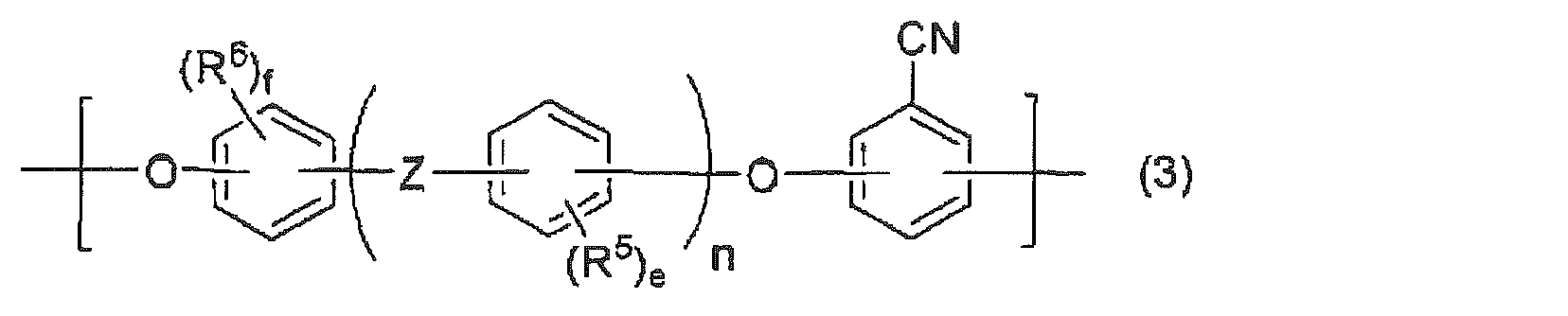
式(3)中、R5およびR6は、それぞれ独立に炭素数1~12の1価の有機基を示し、Zは、単結合、-O-、-S-、-SO2-、>C=O、-CONH-、-COO-または炭素数1~12の2価の有機基を示し、eおよびfは、それぞれ独立に0~4の整数を示し、nは0または1を示す。

式(4)中、R7、R8、Y、m、gおよびhは、それぞれ独立に前記式(2)中のR7、R8、Y、m、gおよびhと同義であり、R5、R6、Z、n、eおよびfは、それぞれ独立に前記式(3)中のR5、R6、Z、n、eおよびfと同義である。
(3)ポリイミド系樹脂
ポリイミド系樹脂としては、特に制限されず、繰り返し単位にイミド結合を含む高分子化合物であればよく、例えば特開2006-199945号公報や特開2008-163107号公報に記載されている方法で合成することができる。
ポリイミド系樹脂としては、特に制限されず、繰り返し単位にイミド結合を含む高分子化合物であればよく、例えば特開2006-199945号公報や特開2008-163107号公報に記載されている方法で合成することができる。
(4)フルオレンポリカーボネート系樹脂
フルオレンポリカーボネート系樹脂としては、特に制限されず、フルオレン部位を含むポリカーボネート樹脂であればよく、例えば特開2008-163194号公報に記載されている方法で合成することができる。
フルオレンポリカーボネート系樹脂としては、特に制限されず、フルオレン部位を含むポリカーボネート樹脂であればよく、例えば特開2008-163194号公報に記載されている方法で合成することができる。
(5)フルオレンポリエステル系樹脂
フルオレンポリエステル系樹脂としては、特に制限されず、フルオレン部位を含むポリエステル樹脂であればよく、例えば特開2010-285505号公報や特開2011-197450号公報に記載されている方法で合成することができる。
フルオレンポリエステル系樹脂としては、特に制限されず、フルオレン部位を含むポリエステル樹脂であればよく、例えば特開2010-285505号公報や特開2011-197450号公報に記載されている方法で合成することができる。
(6)フッ素化芳香族ポリマー系樹脂
フッ素化芳香族ポリマー系樹脂としては、特に制限されないが、少なくとも1つのフッ素を有する芳香族環と、エーテル結合、ケトン結合、スルホン結合、アミド結合、イミド結合およびエステル結合からなる群より選ばれる少なくとも1つの結合を含む繰り返し単位とを含有するポリマーであればよく、例えば特開2008-181121号公報に記載されている方法で合成することができる。
フッ素化芳香族ポリマー系樹脂としては、特に制限されないが、少なくとも1つのフッ素を有する芳香族環と、エーテル結合、ケトン結合、スルホン結合、アミド結合、イミド結合およびエステル結合からなる群より選ばれる少なくとも1つの結合を含む繰り返し単位とを含有するポリマーであればよく、例えば特開2008-181121号公報に記載されている方法で合成することができる。
(7)市販品
透明樹脂の市販品としては、以下の市販品等を挙げることができる。環状オレフィン系樹脂の市販品としては、JSR株式会社製アートン、日本ゼオン株式会社製ゼオノア、三井化学株式会社製APEL、ポリプラスチックス株式会社製TOPASなどを挙げることができる。ポリエーテルサルホン系樹脂の市販品としては、住友化学株式会社製スミカエクセルPESなどを挙げることができる。ポリイミド系樹脂の市販品としては、三菱ガス化学株式会社製ネオプリムLなどを挙げることができる。ポリカーボネート系樹脂の市販品としては、帝人株式会社製ピュアエースなどを挙げることができる。フルオレンポリカーボネート系樹脂の市販品としては、三菱ガス化学株式会社製ユピゼータEP-5000などを挙げることができる。フルオレンポリエステル系樹脂の市販品としては、大阪ガスケミカル株式会社製OKP4HTなどを挙げることができる。アクリル系樹脂の市販品としては、株式会社日本触媒製アクリビュアなどを挙げることができる。シルセスキオキサン系樹脂の市販品としては、新日鐵化学株式会社製シルプラスなどを挙げることができる。
透明樹脂の市販品としては、以下の市販品等を挙げることができる。環状オレフィン系樹脂の市販品としては、JSR株式会社製アートン、日本ゼオン株式会社製ゼオノア、三井化学株式会社製APEL、ポリプラスチックス株式会社製TOPASなどを挙げることができる。ポリエーテルサルホン系樹脂の市販品としては、住友化学株式会社製スミカエクセルPESなどを挙げることができる。ポリイミド系樹脂の市販品としては、三菱ガス化学株式会社製ネオプリムLなどを挙げることができる。ポリカーボネート系樹脂の市販品としては、帝人株式会社製ピュアエースなどを挙げることができる。フルオレンポリカーボネート系樹脂の市販品としては、三菱ガス化学株式会社製ユピゼータEP-5000などを挙げることができる。フルオレンポリエステル系樹脂の市販品としては、大阪ガスケミカル株式会社製OKP4HTなどを挙げることができる。アクリル系樹脂の市販品としては、株式会社日本触媒製アクリビュアなどを挙げることができる。シルセスキオキサン系樹脂の市販品としては、新日鐵化学株式会社製シルプラスなどを挙げることができる。
<近赤外線吸収色素>
光学フィルターに上述の近赤外線反射特性に加えて近赤外線吸収特性を付与し、より優れた近赤外線カット特性を実現する観点から、樹脂製基板は、近赤外線吸収色素を含有することが好ましい。
光学フィルターに上述の近赤外線反射特性に加えて近赤外線吸収特性を付与し、より優れた近赤外線カット特性を実現する観点から、樹脂製基板は、近赤外線吸収色素を含有することが好ましい。
近赤外線吸収色素は、スクアリリウム系化合物、シアニン系化合物、フタロシアニン系化合物、ナフタロシアニン系化合物、クロコニウム系化合物、ジチオール系化合物、ジイモニウム系化合物およびポルフィリン系化合物からなる群より選ばれる少なくとも1種であることが好ましい。近赤外線吸収色素は、スクアリリウム系化合物を少なくとも含むことがより好ましい。近赤外線吸収色素は、スクアリリウム系化合物とその他の近赤外線吸収色素とを含むことがさらに好ましい。
スクアリリウム系化合物の吸収極大波長は、好ましくは600nm以上、さらに好ましくは620nm以上、特に好ましくは650nm以上であり、かつ、好ましくは800nm未満、さらに好ましくは760nm以下、特に好ましくは740nm以下である。吸収極大波長がこのような波長範囲にあると、充分な近赤外線吸収特性と可視光透過率とを両立することができる。
スクアリリウム系化合物とその他の近赤外線吸収色素とを組み合わせて使用する場合、その他の近赤外線吸収色素の少なくとも1種の吸収極大波長は、好ましくは600nm超、さらに好ましくは640nm以上、特に好ましくは670nm以上であり、かつ、好ましくは800nm以下、さらに好ましくは780nm以下、特に好ましくは760nm以下である。その他の近赤外線吸収色素の吸収極大波長がこのような波長範囲にあると、充分な近赤外線吸収特性と可視光透過率とを両立することができるとともに、スクアリリウム系化合物とその他の近赤外線吸収色素とを併用した場合、スクアリリウム系化合物から発生した蛍光をその他の近赤外線吸収色素が効果的に吸収することができ、光学フィルターの散乱光強度を抑制することができる。
その他の近赤外線吸収色素は、具体的には、シアニン系化合物およびフタロシアニン系化合物からなる群より選ばれる少なくとも1種を含むことが好ましく、フタロシアニン系化合物を含むことが特に好ましい。スクアリリウム系化合物と前記化合物とを併用することで、散乱光が少なくカメラ画質がより良好な光学フィルターを得ることができる。
近赤外線吸収色素全体を100重量%とした場合、スクアリリウム系化合物の含有割合は、好ましくは20~95重量%、より好ましくは25~85重量%、特に好ましくは30~80重量%である。スクアリリウム系化合物の含有割合が前記範囲内にあると、良好な可視光透過率と散乱光低減効果とを両立させることができる。また、スクアリリウム系化合物とその他の近赤外線吸収色素は、それぞれの化合物について2種以上を使用してもよい。
樹脂製基板において、近赤外線吸収色素の含有量は、樹脂製基板製造時に用いる透明樹脂100重量部に対して、好ましくは0.01~5.0重量部、より好ましくは0.02~3.5重量部、特に好ましくは0.03~2.5重量部である。近赤外線吸収色素の含有量が前記範囲内にあると、良好な近赤外線吸収特性と高い可視光透過率を両立させることができる。
《スクアリリウム系化合物》
スクアリリウム系化合物としては、式(I)で表されるスクアリリウム系化合物および式(II)で表されるスクアリリウム系化合物からなる群より選ばれる少なくとも1種を含むことが好ましい。以下、それぞれ「化合物(I)」および「化合物(II)」ともいう。
スクアリリウム系化合物としては、式(I)で表されるスクアリリウム系化合物および式(II)で表されるスクアリリウム系化合物からなる群より選ばれる少なくとも1種を含むことが好ましい。以下、それぞれ「化合物(I)」および「化合物(II)」ともいう。
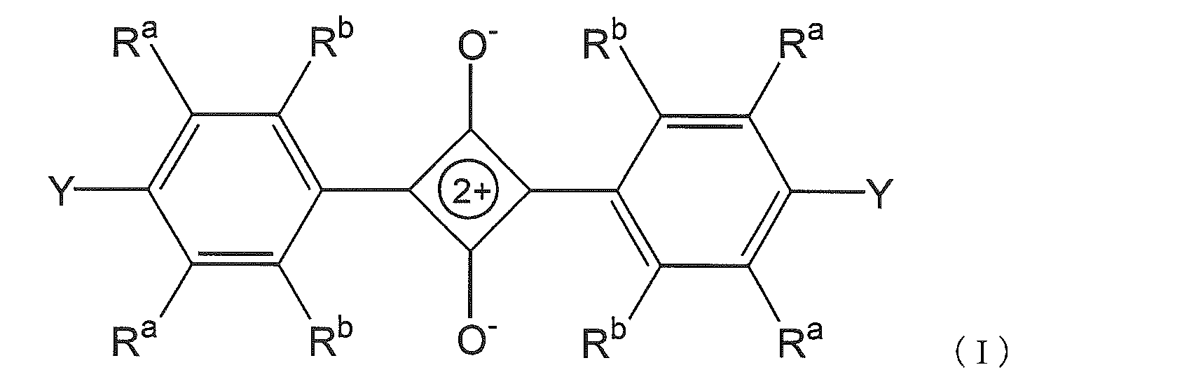
式(I)中、Ra、RbおよびYは、下記(i)または(ii)の条件を満たす。
条件(i)
複数あるRaは、それぞれ独立に水素原子、ハロゲン原子、スルホ基、水酸基、シアノ基、ニトロ基、カルボキシ基、リン酸基、-L1または-NReRf基を表す。ReおよびRfは、それぞれ独立に水素原子、-La、-Lb、-Lc、-Ldまたは-Leを表す。
条件(i)
複数あるRaは、それぞれ独立に水素原子、ハロゲン原子、スルホ基、水酸基、シアノ基、ニトロ基、カルボキシ基、リン酸基、-L1または-NReRf基を表す。ReおよびRfは、それぞれ独立に水素原子、-La、-Lb、-Lc、-Ldまたは-Leを表す。
複数あるRbは、それぞれ独立に水素原子、ハロゲン原子、スルホ基、水酸基、シアノ基、ニトロ基、カルボキシ基、リン酸基、-L1または-NRgRh基を表す。RgおよびRhは、それぞれ独立に水素原子、-La、-Lb、-Lc、-Ld、-Leまたは-C(O)Ri基(Riは、-La、-Lb、-Lc、-Ldまたは-Leを表す。)を表す。
複数あるYは、それぞれ独立に-NRjRk基を表す。RjおよびRkは、それぞれ独立に水素原子、-La、-Lb、-Lc、-Ldまたは-Leを表す。
L1は、La、Lb、Lc、Ld、Le、Lf、LgまたはLhである。
L1は、La、Lb、Lc、Ld、Le、Lf、LgまたはLhである。
前記La~Lhは、
(La)炭素数1~9の脂肪族炭化水素基、
(Lb)炭素数1~9のハロゲン置換アルキル基、
(Lc)炭素数3~14の脂環式炭化水素基、
(Ld)炭素数6~14の芳香族炭化水素基、
(Le)炭素数3~14の複素環基、
(Lf)炭素数1~9のアルコキシ基、
(Lg)炭素数1~9のアシル基、または
(Lh)炭素数1~9のアルコキシカルボニル基
を表し、前記La~Lhは、置換基Lを有していてもよい。
(La)炭素数1~9の脂肪族炭化水素基、
(Lb)炭素数1~9のハロゲン置換アルキル基、
(Lc)炭素数3~14の脂環式炭化水素基、
(Ld)炭素数6~14の芳香族炭化水素基、
(Le)炭素数3~14の複素環基、
(Lf)炭素数1~9のアルコキシ基、
(Lg)炭素数1~9のアシル基、または
(Lh)炭素数1~9のアルコキシカルボニル基
を表し、前記La~Lhは、置換基Lを有していてもよい。
置換基Lは、炭素数1~9の脂肪族炭化水素基、炭素数1~9のハロゲン置換アルキル基、炭素数3~14の脂環式炭化水素基、炭素数6~14の芳香族炭化水素基および炭素数3~14の複素環基からなる群より選ばれる少なくとも1種である。
前記La~Lhは、さらにハロゲン原子、スルホ基、水酸基、シアノ基、ニトロ基、カルボキシ基、リン酸基およびアミノ基からなる群より選ばれる少なくとも1種の原子または基を有していてもよい。
前記La~Lhは、置換基を含めた炭素数の合計が、それぞれ50以下であることが好ましく、炭素数40以下であることが更に好ましく、炭素数30以下であることが特に好ましい。炭素数がこの範囲よりも多いと、色素の合成が困難となる場合があるとともに、単位重量あたりの吸収強度が小さくなってしまう傾向がある。
条件(ii)
1つのベンゼン環上の2つのRaのうちの少なくとも1つが、同じベンゼン環上のYと相互に結合して、窒素原子を少なくとも1つ含む構成原子数5または6の複素環を形成し、前記複素環は置換基を有していてもよく、Rbおよび前記複素環の形成に関与しないRaは、それぞれ独立に前記(i)のRbおよびRaと同義である。
1つのベンゼン環上の2つのRaのうちの少なくとも1つが、同じベンゼン環上のYと相互に結合して、窒素原子を少なくとも1つ含む構成原子数5または6の複素環を形成し、前記複素環は置換基を有していてもよく、Rbおよび前記複素環の形成に関与しないRaは、それぞれ独立に前記(i)のRbおよびRaと同義である。
前記条件(i)におけるRaとしては、好ましくは水素原子、塩素原子、フッ素原子、メチル基、エチル基、n-プロピル基、イソプロピル基、n-ブチル基、sec-ブチル基、tert-ブチル基、シクロヘキシル基、フェニル基、水酸基、アミノ基、ジメチルアミノ基、ニトロ基であり、より好ましくは水素原子、塩素原子、フッ素原子、メチル基、エチル基、n-プロピル基、イソプロピル基、水酸基である。
前記条件(i)におけるRbとしては、好ましくは水素原子、塩素原子、フッ素原子、メチル基、エチル基、n-プロピル基、イソプロピル基、n-ブチル基、sec-ブチル基、tert-ブチル基、シクロヘキシル基、フェニル基、水酸基、アミノ基、ジメチルアミノ基、シアノ基、ニトロ基、アセチルアミノ基、プロピオニルアミノ基、N-メチルアセチルアミノ基、トリフルオロメタノイルアミノ基、ペンタフルオロエタノイルアミノ基、t-ブタノイルアミノ基、シクロヘキシノイルアミノ基であり、より好ましくは水素原子、塩素原子、フッ素原子、メチル基、エチル基、n-プロピル基、イソプロピル基、水酸基、ジメチルアミノ基、ニトロ基、アセチルアミノ基、プロピオニルアミノ基、トリフルオロメタノイルアミノ基、ペンタフルオロエタノイルアミノ基、t-ブタノイルアミノ基、シクロヘキシノイルアミノ基である。
前記Yとしては、好ましくはアミノ基、メチルアミノ基、ジメチルアミノ基、ジエチルアミノ基、ジ-n-プロピルアミノ基、ジイソプロピルアミノ基、ジ-n-ブチルアミノ基、ジ-t-ブチルアミノ基、N-エチル-N-メチルアミノ基、N-シクロヘキシル-N-メチルアミノ基であり、より好ましくはジメチルアミノ基、ジエチルアミノ基、ジ-n-プロピルアミノ基、ジイソプロピルアミノ基、ジ-n-ブチルアミノ基、ジ-t-ブチルアミノ基である。
前記式(I)の条件(ii)における、1つのベンゼン環上の2つのRaのうちの少なくとも1つが、同じベンゼン環上のYと相互に結合して形成される、窒素原子を少なくとも1つ含む構成原子数5または6の複素環としては、例えば、ピロリジン、ピロール、イミダゾール、ピラゾール、ピペリジン、ピリジン、ピペラジン、ピリダジン、ピリミジンおよびピラジン等を挙げることができる。これらの複素環のうち、当該複素環を構成し、かつ、前記ベンゼン環を構成する炭素原子の隣の1つの原子が窒素原子である複素環が好ましく、ピロリジンがさらに好ましい。複素環が有してもよい置換基としては、例えば、置換基Lが挙げられ、好ましくは炭素数1~9の脂肪族炭化水素基である。
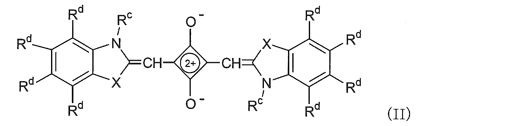
式(II)中、Xは、-O-、-S-、-Se-、>N-Rcまたは>CRd
2を表し;複数あるRcは、それぞれ独立に水素原子、-La、-Lb、-Lc、-Ldまたは-Leを表し;複数あるRdは、それぞれ独立に水素原子、ハロゲン原子、スルホ基、水酸基、シアノ基、ニトロ基、カルボキシ基、リン酸基、-L1または-NReRf基を表し、隣り合うRd同士は連結して置換基を有していてもよい環を形成してもよく;La~Le、L1、ReおよびRfは、前記式(I)において定義したLa~Le、L1、ReおよびRfと同義である。
前記式(II)中のRcとしては、好ましくは水素原子、メチル基、エチル基、n-プロピル基、イソプロピル基、n-ブチル基、sec-ブチル基、tert-ブチル基、n-ペンチル基、n-ヘキシル基、シクロヘキシル基、フェニル基、トルフルオロメチル基、ペンタフルオロエチル基であり、より好ましくは水素原子、メチル基、エチル基、n-プロピル基、イソプロピル基である。
前記式(II)中のRdとしては、好ましくは水素原子、塩素原子、フッ素原子、メチル基、エチル基、n-プロピル基、イソプロピル基、n-ブチル基、sec-ブチル基、tert-ブチル基、n-ペンチル基、n-ヘキシル基、シクロヘキシル基、フェニル基、メトキシ基、トリフルオロメチル基、ペンタフルオロエチル基、4-アミノシクロヘキシル基であり、より好ましくは水素原子、塩素原子、フッ素原子、メチル基、エチル基、n-プロピル基、イソプロピル基、トリフルオロメチル基、ペンタフルオロエチル基である。
前記Xとしては、好ましくは-O-、-S-、-Se-、>N-Me、>N-Et、>CH2、>C(Me)2、>C(Et)2であり、より好ましくは-S-、>C(Me)2、>C(Et)2である。MeおよびEtは、それぞれメチル基およびエチル基を示す。
前記式(II)において、隣り合うRd同士は連結して環を形成してもよい。このような、式(II)においてRcおよびRd結合している環に、隣り合うRd同士が連結して形成された環が付加された構造としては、例えば、ベンゾインドレニン環、α-ナフトイミダゾール環、β-ナフトイミダゾール環、α-ナフトオキサゾール環、β-ナフトオキサゾール環、α-ナフトチアゾール環、β-ナフトチアダゾール環、α-ナフトセレナゾール環、β-ナフトセレナゾール環を挙げることができる。
化合物(I)および化合物(II)は、下記式(I-1)および下記式(II-1)のような記載方法に加え、下記式(I-2)および下記式(II-2)のように共鳴構造を取るような記載方法でも構造を表すことができる。つまり、下記式(I-1)と下記式(I-2)の違い、および下記式(II-1)と下記式(II-2)の違いは構造の記載方法のみであり、化合物としてはどちらも同一のものを表す。本発明中では特に断りのない限り、下記式(I-1)および下記式(II-1)のような記載方法にてスクアリリウム系化合物の構造を表すものとする。
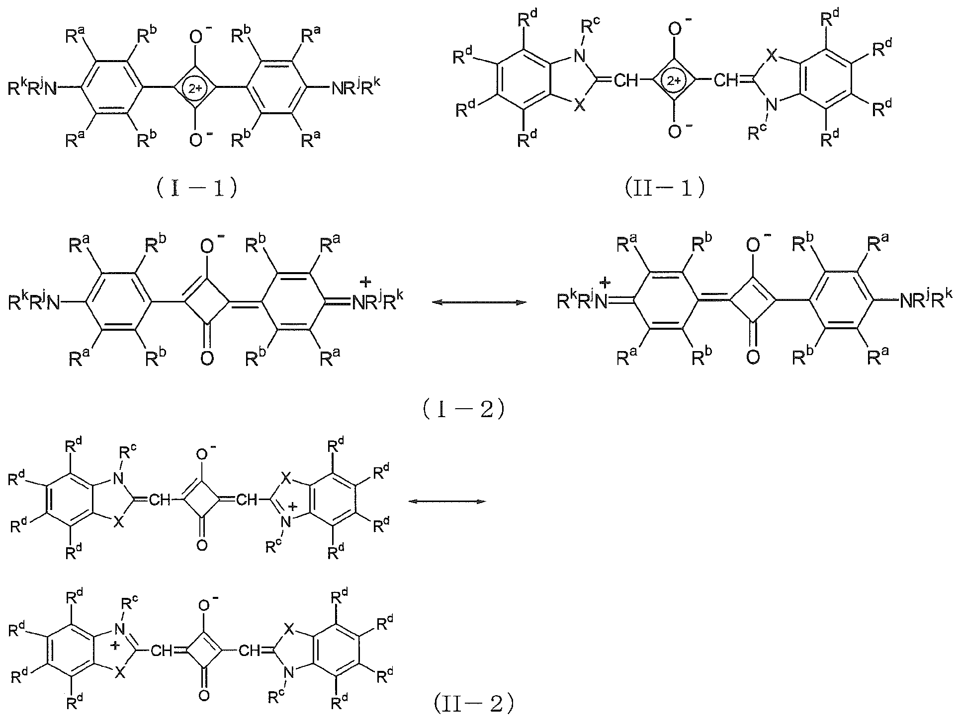
化合物(I)および化合物(II)は、それぞれ上記式(I)および上記式(II)の要件を満たせば特に構造は限定されないが、例えば上記式(I-1)および上記式(II-1)のように構造を表した場合、中央の四員環に結合している左右の置換基は同一であっても異なっていてもよいが、同一であった方が合成上容易であるため好ましい。なお、例えば、下記式(I-3)で表される化合物と下記式(I-4)で表される化合物は、同一の化合物であると見なすことができる。

化合物(I)および化合物(II)は、一般的に知られている方法で合成すればよく、例えば、特開平1-228960号公報、特開2001-40234号公報、特許第3196383号公報等に記載されている方法等を参照して合成することができる。
<近紫外線吸収剤>
樹脂製基板は、近赤外線吸収色素に加え、さらに、近紫外線吸収剤を含有することができる。近紫外線吸収剤としては、例えば、アゾメチン系化合物、インドール系化合物、ベンゾトリアゾール系化合物およびトリアジン系化合物からなる群より選ばれる少なくとも1種が挙げられる。近紫外線吸収剤は、波長300~420nmに少なくとも一つの吸収極大を持つことが好ましい。このような樹脂製基板を用いることにより、近紫外線波長領域においても、視野角の広い光学フィルターを得ることができる。
樹脂製基板は、近赤外線吸収色素に加え、さらに、近紫外線吸収剤を含有することができる。近紫外線吸収剤としては、例えば、アゾメチン系化合物、インドール系化合物、ベンゾトリアゾール系化合物およびトリアジン系化合物からなる群より選ばれる少なくとも1種が挙げられる。近紫外線吸収剤は、波長300~420nmに少なくとも一つの吸収極大を持つことが好ましい。このような樹脂製基板を用いることにより、近紫外線波長領域においても、視野角の広い光学フィルターを得ることができる。
以上のスクアリリウム系化合物、フタロシアニン系化合物、シアニン系化合物、近紫外線吸収剤およびその他の色素は、一般的に知られている方法で合成することができ、例えば、特許第3366697号公報、特許第2846091号公報、特許第2864475号公報、特許第3703869号公報、特開昭60-228448号公報、特開平1-146846号公報、特開平1-228960号公報、特許第4081149号公報、特開昭63-124054号公報、「フタロシアニン -化学と機能―」(アイピーシー、1997年)、特開2007-169315号公報、特開2009-108267号公報、特開2010-241873号公報、特許第3699464号公報、特許第4740631号公報等に記載されている方法を参照して合成することができる。
<その他成分>
樹脂製基板は、本発明の効果を損なわない範囲において、さらに、酸化防止剤、近紫外線吸収剤以外の紫外線吸収剤、蛍光消光剤および金属錯体系化合物等の添加剤を含有してもよい。また、後述するキャスト成形により樹脂製基板を製造する場合には、レベリング剤や消泡剤を添加することで樹脂製基板の製造を容易にすることができる。これらのその他成分は、1種単独で用いてもよいし、2種以上を併用してもよい。
樹脂製基板は、本発明の効果を損なわない範囲において、さらに、酸化防止剤、近紫外線吸収剤以外の紫外線吸収剤、蛍光消光剤および金属錯体系化合物等の添加剤を含有してもよい。また、後述するキャスト成形により樹脂製基板を製造する場合には、レベリング剤や消泡剤を添加することで樹脂製基板の製造を容易にすることができる。これらのその他成分は、1種単独で用いてもよいし、2種以上を併用してもよい。
酸化防止剤としては、例えば、2,6-ジ-t-ブチル-4-メチルフェノール、2,2'-ジオキシ-3,3'-ジ-t-ブチル-5,5'-ジメチルジフェニルメタン、およびテトラキス[メチレン-3-(3,5-ジ-t-ブチル-4-ヒドロキシフェニル)プロピオネート]メタンが挙げられる。
なお、これらの添加剤は、樹脂製基板を製造する際に、透明樹脂などとともに混合してもよいし、透明樹脂を製造する際に添加してもよい。また、添加剤の添加量は、所望の特性に応じて適宜選択されるものであるが、透明樹脂100重量部に対して、通常0.01~5.0重量部、好ましくは0.05~2.0重量部である。
<樹脂製基板の製造方法>
樹脂製基板は、例えば、溶融成形またはキャスト成形により形成することができ、必要により、成形後に、反射防止剤、ハードコート剤および帯電防止剤等を1種または2種以上含むコーティング剤をコーティングする方法により製造することができる。なお、以下では、近赤外線吸収色素を配合する例をもとに説明する。
樹脂製基板は、例えば、溶融成形またはキャスト成形により形成することができ、必要により、成形後に、反射防止剤、ハードコート剤および帯電防止剤等を1種または2種以上含むコーティング剤をコーティングする方法により製造することができる。なお、以下では、近赤外線吸収色素を配合する例をもとに説明する。
(1)溶融成形
樹脂製基板は、例えば、透明樹脂と近赤外線吸収色素とを溶融混練りして得られたペレットを溶融成形する方法;透明樹脂と近赤外線吸収色素とを含有する樹脂組成物を溶融成形する方法;透明樹脂、近赤外線吸収色素および溶媒を含有する樹脂組成物から溶媒を除去して得られたペレットを溶融成形する方法により製造することができる。溶融成形方法としては、例えば、射出成形、溶融押出成形、ブロー成形が挙げられる。
樹脂製基板は、例えば、透明樹脂と近赤外線吸収色素とを溶融混練りして得られたペレットを溶融成形する方法;透明樹脂と近赤外線吸収色素とを含有する樹脂組成物を溶融成形する方法;透明樹脂、近赤外線吸収色素および溶媒を含有する樹脂組成物から溶媒を除去して得られたペレットを溶融成形する方法により製造することができる。溶融成形方法としては、例えば、射出成形、溶融押出成形、ブロー成形が挙げられる。
(2)キャスト成形
樹脂製基板は、例えば、透明樹脂、近赤外線吸収色素および溶媒を含有する樹脂組成物を適当な基材の上に塗布して溶媒を除去する方法;近赤外線吸収色素を含有する硬化性樹脂組成物を適当な基材の上に塗布して乾燥および硬化させる方法により製造することもできる。
樹脂製基板は、例えば、透明樹脂、近赤外線吸収色素および溶媒を含有する樹脂組成物を適当な基材の上に塗布して溶媒を除去する方法;近赤外線吸収色素を含有する硬化性樹脂組成物を適当な基材の上に塗布して乾燥および硬化させる方法により製造することもできる。
前記基材としては、例えば、ガラス板、スチールベルト、スチールドラムおよび透明樹脂フィルム(例えば、ポリエステルフィルム、環状オレフィン系樹脂フィルム)が挙げられる。
樹脂製基板は、基材から剥離することにより得ることができ、また、本発明の効果を損なわない限り、基材から剥離せずに基材と塗膜との積層体を樹脂製基板としてもよい。
さらに、ガラス板、石英製部品または透明プラスチック製部品等の光学部品に、前記樹脂組成物をコーティングして溶媒を乾燥させる方法、または、前記硬化性樹脂組成物をコーティングして乾燥および硬化させる方法等により、光学部品上に直接樹脂製基板を形成することもできる。
さらに、ガラス板、石英製部品または透明プラスチック製部品等の光学部品に、前記樹脂組成物をコーティングして溶媒を乾燥させる方法、または、前記硬化性樹脂組成物をコーティングして乾燥および硬化させる方法等により、光学部品上に直接樹脂製基板を形成することもできる。
前記溶媒としては通常有機合成などに用いられる溶媒であれば特に限定されないが、例えば、ヘキサン、シクロヘキサンなどの炭化水素類;メタノール、エタノール、イソプロパノール、ブタノール、オクタノール等のアルコール類;アセトン、メチルエチルケトン、メチルイソブチルケトン、シクロヘキサノン等のケトン類;酢酸エチル、酢酸ブチル、乳酸エチル、γ-ブチロラクトン、プロピレングリコールモノメチルエーテルアセテート、プロピレングリコールモノエチルエーテルアセテート等のエステル類;エチレングリコールモノメチルエーテル、ジエチレングリコールモノブチルエーテル等のエーテル類;ベンゼン、トルエン、キシレン等の芳香族炭化水素類;塩化メチレン、クロロホルム、四塩化炭素などのハロゲン化炭化水素類;ジメチルホルムアミド、ジメチルアセトアミド、N-メチルピロリドン等のアミド類を挙げることができる。これらの溶媒は、1種単独で用いてもよいし、2種以上を併用してもよい。
前記方法で得られた樹脂製基板中の残留溶媒量は可能な限り少ない方がよい。具体的には、前記残留溶媒量は、樹脂製基板の重さに対して、好ましくは3重量%以下、より好ましくは1重量%以下、さらに好ましくは0.5重量%以下である。残留溶媒量が前記範囲にあると、変形や特性が変化しにくい、所望の機能を容易に発揮できる樹脂製基板が得られる。
[近赤外線反射膜]
本発明の光学フィルターを構成する近赤外線反射膜は、近赤外線を反射する能力を有する膜である。本発明では、近赤外線反射膜は樹脂製基板の片面に設けてもよいし、両面に設けてもよい。片面に設ける場合、製造コストや製造容易性に優れ、両面に設ける場合、高い強度を有し、反りの生じにくい光学フィルターを得ることができる。光学フィルターを固体撮像素子用途に使用する場合は、カメラモジュールへの実装工程の容易さなどの観点から光学フィルターの反りが小さいことが好ましいため、近赤外線反射膜を樹脂製基板の両側に有することがより好ましい。
本発明の光学フィルターを構成する近赤外線反射膜は、近赤外線を反射する能力を有する膜である。本発明では、近赤外線反射膜は樹脂製基板の片面に設けてもよいし、両面に設けてもよい。片面に設ける場合、製造コストや製造容易性に優れ、両面に設ける場合、高い強度を有し、反りの生じにくい光学フィルターを得ることができる。光学フィルターを固体撮像素子用途に使用する場合は、カメラモジュールへの実装工程の容易さなどの観点から光学フィルターの反りが小さいことが好ましいため、近赤外線反射膜を樹脂製基板の両側に有することがより好ましい。
近赤外線反射膜としては、例えば、アルミ蒸着膜、貴金属薄膜、酸化インジウムを主成分とし酸化錫を少量含有させた金属酸化物微粒子を分散させた樹脂膜、高屈折率材料層と低屈折率材料層とを交互に積層した誘電体多層膜が挙げられる。近赤外線反射膜の中では、高屈折率材料層と低屈折率材料層とを交互に積層した誘電体多層膜がより好ましい。
高屈折率材料層を構成する材料としては、屈折率が1.7より大きい材料を用いることができ、屈折率が通常は1.7を超えて2.5以下の材料が選択される。このような材料としては、例えば、酸化チタン、酸化ジルコニウム、五酸化タンタル、五酸化ニオブ、酸化ランタン、酸化イットリウム、酸化亜鉛、硫化亜鉛、または、酸化インジウム等を主成分とし、酸化チタン、酸化錫および/または酸化セリウム等を少量(例えば、主成分に対して0~10重量%)含有させたものが挙げられる。
低屈折率材料層を構成する材料としては、屈折率が1.7以下の材料を用いることができ、屈折率が通常は1.2~1.7の材料が選択される。このような材料としては、例えば、シリカ、アルミナ、フッ化ランタン、フッ化マグネシウムおよび六フッ化アルミニウムナトリウムが挙げられる。
誘電体多層膜は、屈折率が1.7を超えて2.5以下である高屈折率材料層と屈折率が1.2以上1.7以下である低屈折材料層とが交互に積層された多層膜であることが好ましい。
上記屈折率は、波長550nmの光における屈折率である。屈折率は、例えば以下の様にして測定することができる。ガラス基板上に屈折率を測定する対象層をそれぞれ単層で蒸着成膜したサンプルを作製し、株式会社日立ハイテクノロジーズ製の分光光度計(U-4100)を用いて、作製したサンプルの透過率および反射率を測定する(透過率および反射率はサンプル面の垂直方向に対して5°の角度から測定を行う)。得られた透過率、反射率データを光学薄膜設計ソフト(Essential Macleod、Thin Film Center社製)に入力し、関数フィッティングを行うことで各対象層の波長550nmの光に対する屈折率を求める。
高屈折率材料層と低屈折率材料層とを積層する方法については、これらの材料層を積層した誘電体多層膜が形成される限り特に制限はない。例えば、樹脂製基板上に、直接、CVD法、スパッタ法、真空蒸着法、イオンアシスト蒸着法またはイオンプレーティング法等により、高屈折率材料層と低屈折率材料層とを交互に積層した誘電体多層膜を形成することができる。
高屈折率材料層および低屈折率材料層の各層の厚さは、通常、遮断しようとする近赤外線波長をλ(nm)とすると、0.1λ~0.5λの厚さが好ましい。λ(nm)の値としては、例えば700~1400nm、好ましくは750~1300nmである。厚さがこの範囲であると、屈折率(n)と物理膜厚(d)との積(n×d)がλ/4で算出される光学膜厚と高屈折率材料層および低屈折率材料層の各層の厚さとがほぼ同じ値となって、反射・屈折の光学的特性の関係から、特定波長の遮断・透過を容易にコントロールできる傾向にある。
誘電体多層膜における高屈折率材料層と低屈折率材料層との合計の積層数は、光学フィルター全体として5~60層であることが好ましく、10~50層であることがより好ましく、30~50層であることがさらに好ましい。
本発明では、例えば、高屈折率材料層および低屈折率材料層を構成する材料、高屈折率材料層および低屈折率材料層の各層の厚さ、積層の順番、積層数を適切に選択することで、例えば波長800~1200nmの領域において、フィルターの垂直方向に対して45°の入射角の光線に対しても、充分な反射特性を有する光学フィルターを得ることができる。
ここで、上記条件を最適化するには、上述したように、例えば光学薄膜設計ソフト(例えば、Essential Macleod、Thin Film Center社製)を用い、波長800~1200nmの領域の45°反射率が高くなるようにパラメーターを設定すればよい。上記ソフトの場合、例えば、波長800~1200nmの目標透過率を0%などとした上で、Incident Angleの値を45°にし、Target Toleranceの値を0.5以下などとすることが挙げられる。このようにして上記条件を最適化することで、45°反射率を高くすることができる。
[その他の機能膜]
本発明の光学フィルターには、本発明の効果を損なわない範囲において、樹脂製基板と誘電体多層膜等の近赤外線反射膜との間などに、樹脂製基板や近赤外線反射膜の表面硬度の向上、耐薬品性の向上、帯電防止および傷消し等の目的で、反射防止膜、ハードコート膜および帯電防止膜等の機能膜を適宜設けることができる。
本発明の光学フィルターには、本発明の効果を損なわない範囲において、樹脂製基板と誘電体多層膜等の近赤外線反射膜との間などに、樹脂製基板や近赤外線反射膜の表面硬度の向上、耐薬品性の向上、帯電防止および傷消し等の目的で、反射防止膜、ハードコート膜および帯電防止膜等の機能膜を適宜設けることができる。
樹脂製基板と機能膜および/または近赤外線反射膜との密着性や、機能膜と近赤外線反射膜との密着性を上げる目的で、樹脂製基板や機能膜の表面にコロナ処理やプラズマ処理等の表面処理をしてもよい。
[光学フィルターの特性等]
本発明の光学フィルターは、前記透明樹脂製基板とその少なくとも片面に形成された前記近赤外線反射膜とを有する。このため、本発明の光学フィルターは、透過率特性と、近赤外線反射特性、特に波長800~1200nmという広範囲の赤外領域において高入射角の光線に対する光線反射特性とに優れる。このような光学フィルターを固体撮像素子用途に使用すると、高画質化を達成することができ、具体的にはゴーストなどが少ない良好なカメラ画像を得ることができる。
本発明の光学フィルターは、前記透明樹脂製基板とその少なくとも片面に形成された前記近赤外線反射膜とを有する。このため、本発明の光学フィルターは、透過率特性と、近赤外線反射特性、特に波長800~1200nmという広範囲の赤外領域において高入射角の光線に対する光線反射特性とに優れる。このような光学フィルターを固体撮像素子用途に使用すると、高画質化を達成することができ、具体的にはゴーストなどが少ない良好なカメラ画像を得ることができる。
また、樹脂製基板に好ましくは配合される近赤外線吸収色素の少なくとも1種として、例えば波長600~800nmに吸収極大を有する色素を用いることで、近赤外光を効率的に吸収することができる。したがって、このような透明樹脂製基板と近赤外線反射膜と組み合わせることにより、優れた近赤外線吸収・反射特性を有する光学フィルターを得ることができる。
[光学フィルターの用途]
本発明の光学フィルターは、上述したような優れた近赤外線カット特性等を有する。したがって、カメラモジュールのCCDやCMOSイメージセンサー等の固体撮像素子の視感度補正用として有用である。特に、デジタルスチルカメラ、携帯電話用カメラ、デジタルビデオカメラ、パーソナルコンピューター用カメラ、監視カメラ、自動車用カメラ、テレビ、カーナビゲーションシステム用車載装置、携帯情報端末、ビデオゲーム機、携帯ゲーム機、指紋認証システム用装置、デジタルミュージックプレーヤー等に有用である。さらに、自動車や建物等のガラス板等に装着される熱線カットフィルターなどとしても有用である。
本発明の光学フィルターは、上述したような優れた近赤外線カット特性等を有する。したがって、カメラモジュールのCCDやCMOSイメージセンサー等の固体撮像素子の視感度補正用として有用である。特に、デジタルスチルカメラ、携帯電話用カメラ、デジタルビデオカメラ、パーソナルコンピューター用カメラ、監視カメラ、自動車用カメラ、テレビ、カーナビゲーションシステム用車載装置、携帯情報端末、ビデオゲーム機、携帯ゲーム機、指紋認証システム用装置、デジタルミュージックプレーヤー等に有用である。さらに、自動車や建物等のガラス板等に装着される熱線カットフィルターなどとしても有用である。
〔固体撮像装置〕
本発明の固体撮像装置は、本発明の光学フィルターを具備する。ここで、固体撮像装置とは、CCDやCMOSイメージセンサー等といった固体撮像素子を備えたイメージセンサーであり、具体的にはデジタルスチルカメラ、携帯電話用カメラ、デジタルビデオカメラ等である。例えば、本発明のカメラモジュールは、本発明の光学フィルターを具備する。
本発明の固体撮像装置は、本発明の光学フィルターを具備する。ここで、固体撮像装置とは、CCDやCMOSイメージセンサー等といった固体撮像素子を備えたイメージセンサーであり、具体的にはデジタルスチルカメラ、携帯電話用カメラ、デジタルビデオカメラ等である。例えば、本発明のカメラモジュールは、本発明の光学フィルターを具備する。
以下、実施例に基づいて本発明をより具体的に説明するが、本発明はこれら実施例に何ら限定されるものではない。なお、「部」は、特に断りのない限り「重量部」を意味する。また、各物性値の測定方法および物性の評価方法は以下のとおりである。
<分子量>
樹脂の分子量は、各樹脂の溶媒への溶解性等を考慮し、下記(a)または(b)の方法にて測定を行った。なお、後述する樹脂合成例3で合成した樹脂については、これらの方法による分子量の測定ではなく、下記方法(c)による対数粘度の測定を行った。
樹脂の分子量は、各樹脂の溶媒への溶解性等を考慮し、下記(a)または(b)の方法にて測定を行った。なお、後述する樹脂合成例3で合成した樹脂については、これらの方法による分子量の測定ではなく、下記方法(c)による対数粘度の測定を行った。
(a)ウオターズ(WATERS)社製GPC装置(150C型、カラム:東ソー社製Hタイプカラム、展開溶媒:o-ジクロロベンゼン)を用い、標準ポリスチレン換算の重量平均分子量(Mw)および数平均分子量(Mn)を測定した。
(b)東ソー社製GPC装置(HLC-8220型、カラム:TSKgelα-M、展開溶媒:テトラヒドロフラン)を用い、標準ポリスチレン換算の重量平均分子量(Mw)および数平均分子量(Mn)を測定した。
(c)ポリイミド樹脂溶液の一部を無水メタノールに投入してポリイミド樹脂を析出させ、ろ過して未反応単量体から分離した。80℃で12時間真空乾燥して得られたポリイミド0.1gをN-メチル-2-ピロリドン20mLに溶解し、キャノン-フェンスケ粘度計を使用して、30℃における対数粘度(μ)を下記式により求めた。
μ={ln(ts/t0)}/C
t0:溶媒の流下時間
ts:希薄高分子溶液の流下時間
C:0.5g/dL
<ガラス転移温度(Tg)>
樹脂のガラス転移温度(Tg)は、エスアイアイ・ナノテクノロジーズ株式会社製の示差走査熱量計(DSC6200)を用いて、昇温速度:毎分20℃、窒素気流下で測定した。
t0:溶媒の流下時間
ts:希薄高分子溶液の流下時間
C:0.5g/dL
<ガラス転移温度(Tg)>
樹脂のガラス転移温度(Tg)は、エスアイアイ・ナノテクノロジーズ株式会社製の示差走査熱量計(DSC6200)を用いて、昇温速度:毎分20℃、窒素気流下で測定した。
<分光透過率および反射率>
樹脂製基板の吸収極大波長、ならびに光学フィルターの各波長領域における透過率および反射率は、株式会社日立ハイテクノロジーズ製の分光光度計(U-4100)を用いて測定した。
樹脂製基板の吸収極大波長、ならびに光学フィルターの各波長領域における透過率および反射率は、株式会社日立ハイテクノロジーズ製の分光光度計(U-4100)を用いて測定した。
ここで、光学フィルターの垂直方向から測定した場合の透過率では、図1(a)のようにフィルター面に対して垂直に透過した光を測定した。樹脂製基板の吸収極大波長を測定する場合も、同様にして当該基板の透過率を測定し、吸収極大波長を求めた。なお、これらの透過率は、光がフィルター面に対して垂直に入射する条件で、前記分光光度計を使用して測定したものである。
また、光学フィルターの垂直方向に対して45°または5°の角度から測定した場合の反射率では、図1(b)または(c)のような装置付属の治具に光学フィルターを設置して測定を行った。反射率は、樹脂製基板の両面に蒸着膜を成膜した場合は最初に蒸着膜を成膜した面(1面目)をA面、2番目に蒸着した面(2面目)をB面とし、樹脂製基板の片面に蒸着膜を成膜した場合は蒸着膜を成膜していない面をA面、蒸着膜を成膜した面をB面とし、A面側およびB面側から光が入射した場合の反射率を測定した。なお、これらの反射率は、光がフィルター面の垂直方向に対して45°または5°の角度で入射する条件で、前記分光光度計を使用して測定したものである。
<ゴースト>
市販のデジタルカメラ(ソニー株式会社製 DSC-RX100)のセンサー上に配置されている光学フィルターを取り除いた後、実施例または比較例で得られた光学フィルターを配置し、撮影を行った。撮影した画像を映し出し、ゴースト光の発生有無を目視で確認した。ゴースト光の発生が認められた場合をBB、ゴースト光の発生が認められなかった場合をAAとした。
市販のデジタルカメラ(ソニー株式会社製 DSC-RX100)のセンサー上に配置されている光学フィルターを取り除いた後、実施例または比較例で得られた光学フィルターを配置し、撮影を行った。撮影した画像を映し出し、ゴースト光の発生有無を目視で確認した。ゴースト光の発生が認められた場合をBB、ゴースト光の発生が認められなかった場合をAAとした。
<樹脂合成例1>
下記式(a)で表される8-メチル-8-メトキシカルボニルテトラシクロ[4.4.0.12,5.17,10]ドデカ-3-エン(以下「DNM」ともいう。)100部、1-ヘキセン(分子量調節剤)18部およびトルエン(開環重合反応用溶媒)300部を、窒素置換した反応容器に仕込み、この溶液を80℃に加熱した。次いで、反応容器内の溶液に、重合触媒として、トリエチルアルミニウムのトルエン溶液(濃度0.6mol/リットル)0.2部と、メタノール変性の六塩化タングステンのトルエン溶液(濃度0.025mol/リットル)0.9部とを添加し、この溶液を80℃で3時間加熱攪拌することにより開環重合反応させて開環重合体溶液を得た。この重合反応における重合転化率は97%であった。
下記式(a)で表される8-メチル-8-メトキシカルボニルテトラシクロ[4.4.0.12,5.17,10]ドデカ-3-エン(以下「DNM」ともいう。)100部、1-ヘキセン(分子量調節剤)18部およびトルエン(開環重合反応用溶媒)300部を、窒素置換した反応容器に仕込み、この溶液を80℃に加熱した。次いで、反応容器内の溶液に、重合触媒として、トリエチルアルミニウムのトルエン溶液(濃度0.6mol/リットル)0.2部と、メタノール変性の六塩化タングステンのトルエン溶液(濃度0.025mol/リットル)0.9部とを添加し、この溶液を80℃で3時間加熱攪拌することにより開環重合反応させて開環重合体溶液を得た。この重合反応における重合転化率は97%であった。

このようにして得られた開環重合体溶液1,000部をオートクレーブに仕込み、この開環重合体溶液に、RuHCl(CO)[P(C6H5)3]3を0.12部添加し、水素ガス圧100kg/cm2、反応温度165℃の条件下で、3時間加熱撹拌して水素添加反応を行った。
得られた反応溶液(水素添加重合体溶液)を冷却した後、水素ガスを放圧した。この反応溶液を大量のメタノール中に注いで凝固物を分離回収し、これを乾燥して、水素添加重合体(以下「樹脂A」ともいう。)を得た。得られた樹脂Aは、数平均分子量(Mn)が32,000、重量平均分子量(Mw)が137,000であり、ガラス転移温度(Tg)が165℃であった。
<樹脂合成例2>
3Lの4つ口フラスコに2,6-ジフルオロベンゾニトリル35.12g(0.253mol)、9,9-ビス(4-ヒドロキシフェニル)フルオレン87.60g(0.250mol)、炭酸カリウム41.46g(0.300mol)、N,N-ジメチルアセトアミド(以下「DMAc」ともいう。)443gおよびトルエン111gを添加した。続いて、4つ口フラスコに温度計、撹拌機、窒素導入管付き三方コック、ディーンスターク管および冷却管を取り付けた。
3Lの4つ口フラスコに2,6-ジフルオロベンゾニトリル35.12g(0.253mol)、9,9-ビス(4-ヒドロキシフェニル)フルオレン87.60g(0.250mol)、炭酸カリウム41.46g(0.300mol)、N,N-ジメチルアセトアミド(以下「DMAc」ともいう。)443gおよびトルエン111gを添加した。続いて、4つ口フラスコに温度計、撹拌機、窒素導入管付き三方コック、ディーンスターク管および冷却管を取り付けた。
次いで、フラスコ内を窒素置換した後、得られた溶液を140℃で3時間反応させ、生成する水をディーンスターク管から随時取り除いた。水の生成が認められなくなったところで、徐々に温度を160℃まで上昇させ、そのままの温度で6時間反応させた。
室温(25℃)まで冷却後、生成した塩をろ紙で除去し、ろ液をメタノールに投じて再沈殿させ、ろ別によりろ物(残渣)を単離した。得られたろ物を60℃で一晩真空乾燥し、白色粉末(以下「樹脂B」ともいう。)を得た(収率95%)。得られた樹脂Bは、数平均分子量(Mn)が75,000、重量平均分子量(Mw)が188,000であり、ガラス転移温度(Tg)が285℃であった。
<樹脂合成例3>
温度計、撹拌器、窒素導入管、側管付き滴下ロート、ディーンスターク管および冷却管を備えた500mLの5つ口フラスコに、窒素気流下、1,4-ビス(4-アミノ-α,α-ジメチルベンジル)ベンゼン27.66g(0.08モル)および4,4'-ビス(4-アミノフェノキシ)ビフェニル7.38g(0.02モル)を入れて、γ―ブチロラクトン68.65gおよびN,N-ジメチルアセトアミド17.16gに溶解させた。得られた溶液を、氷水バスを用いて5℃に冷却し、同温に保ちながら1,2,4,5-シクロヘキサンテトラカルボン酸二無水物22.62g(0.1モル)およびイミド化触媒としてトリエチルアミン0.50g(0.005モル)を一括添加した。添加終了後、180℃に昇温し、随時留出液を留去させながら、6時間還流させた。反応終了後、内温が100℃になるまで空冷した後、N,N-ジメチルアセトアミド143.6gを加えて希釈し、攪拌しながら冷却し、固形分濃度20重量%のポリイミド樹脂溶液264.16gを得た。このポリイミド樹脂溶液の一部を1Lのメタノール中に注ぎいれてポリイミドを沈殿させた。濾別したポリイミドをメタノールで洗浄した後、100℃の真空乾燥機中で24時間乾燥させて白色粉末(以下「樹脂C」ともいう。)を得た。得られた樹脂CのIRスペクトルを測定したところ、イミド基に特有の1704cm-1、1770cm-1の吸収が見られた。得られた樹脂Cは、ガラス転移温度(Tg)が310℃であり、対数粘度が0.87であった。
温度計、撹拌器、窒素導入管、側管付き滴下ロート、ディーンスターク管および冷却管を備えた500mLの5つ口フラスコに、窒素気流下、1,4-ビス(4-アミノ-α,α-ジメチルベンジル)ベンゼン27.66g(0.08モル)および4,4'-ビス(4-アミノフェノキシ)ビフェニル7.38g(0.02モル)を入れて、γ―ブチロラクトン68.65gおよびN,N-ジメチルアセトアミド17.16gに溶解させた。得られた溶液を、氷水バスを用いて5℃に冷却し、同温に保ちながら1,2,4,5-シクロヘキサンテトラカルボン酸二無水物22.62g(0.1モル)およびイミド化触媒としてトリエチルアミン0.50g(0.005モル)を一括添加した。添加終了後、180℃に昇温し、随時留出液を留去させながら、6時間還流させた。反応終了後、内温が100℃になるまで空冷した後、N,N-ジメチルアセトアミド143.6gを加えて希釈し、攪拌しながら冷却し、固形分濃度20重量%のポリイミド樹脂溶液264.16gを得た。このポリイミド樹脂溶液の一部を1Lのメタノール中に注ぎいれてポリイミドを沈殿させた。濾別したポリイミドをメタノールで洗浄した後、100℃の真空乾燥機中で24時間乾燥させて白色粉末(以下「樹脂C」ともいう。)を得た。得られた樹脂CのIRスペクトルを測定したところ、イミド基に特有の1704cm-1、1770cm-1の吸収が見られた。得られた樹脂Cは、ガラス転移温度(Tg)が310℃であり、対数粘度が0.87であった。
<樹脂合成例4>
9,9-ビス{4-(2-ヒドロキシエトキシ)フェニル}フルオレン9.167kg(20.90モル)、ビスフェノールA 4.585kg(20.084モル)、ジフェニルカーボネート9.000kg(42.01モル)、および炭酸水素ナトリウム0.02066kg(2.459×10⁻⁴モル)を、攪拌機および留出装置を備えた50L反応器に入れ、窒素雰囲気で760Torrの下、1時間かけて215℃に加熱・攪拌した。その後、15分かけて減圧度を150Torrに調整し、215℃、150Torrの条件下で20分間保持し、エステル交換反応を行った。さらに37.5℃/Hrの速度で240℃まで昇温し、240℃、150Torrで10分間保持した。その後、10分かけて120Torrに調整し、240℃、120Torrで70分間保持した。その後、10分かけて100Torrに調整し、240℃、100Torrで10分間保持した。更に40分かけて1Torr以下とし、240℃、1Torr以下の条件下で10分間攪拌して重合反応を行った。反応終了後、反応器内に窒素を導入し加圧にし、生成したポリカーボネート樹脂(以下「樹脂D」ともいう。)をペレット化しながら抜き出した。得られた樹脂Dは、重量平均分子量(Mw)が41,000であり、ガラス転移温度(Tg)が152℃であった。
9,9-ビス{4-(2-ヒドロキシエトキシ)フェニル}フルオレン9.167kg(20.90モル)、ビスフェノールA 4.585kg(20.084モル)、ジフェニルカーボネート9.000kg(42.01モル)、および炭酸水素ナトリウム0.02066kg(2.459×10⁻⁴モル)を、攪拌機および留出装置を備えた50L反応器に入れ、窒素雰囲気で760Torrの下、1時間かけて215℃に加熱・攪拌した。その後、15分かけて減圧度を150Torrに調整し、215℃、150Torrの条件下で20分間保持し、エステル交換反応を行った。さらに37.5℃/Hrの速度で240℃まで昇温し、240℃、150Torrで10分間保持した。その後、10分かけて120Torrに調整し、240℃、120Torrで70分間保持した。その後、10分かけて100Torrに調整し、240℃、100Torrで10分間保持した。更に40分かけて1Torr以下とし、240℃、1Torr以下の条件下で10分間攪拌して重合反応を行った。反応終了後、反応器内に窒素を導入し加圧にし、生成したポリカーボネート樹脂(以下「樹脂D」ともいう。)をペレット化しながら抜き出した。得られた樹脂Dは、重量平均分子量(Mw)が41,000であり、ガラス転移温度(Tg)が152℃であった。
<樹脂合成例5>
反応器に、9,9-ビス{4-(2-ヒドロキシエトキシ)-3,5-ジメチルフェニル}フルオレン0.8モル、エチレングリコール2.2モルおよびイソフタル酸ジメチル1.0モルを加え、攪拌しながら徐々に加熱溶融してエステル交換反応を行った後、酸化ゲルマニウム20×10-4モルを加え、290℃、1Torr以下に到達するまで徐々に昇温および減圧を行いながらエチレングリコールを除去した。この後、内容物を反応器から取り出し、ポリエステル樹脂(以下「樹脂E」ともいう。)のペレットを得た。得られた樹脂Eは、数平均分子量(Mn)が40,000であり、ガラス転移温度(Tg)が145℃であった。
反応器に、9,9-ビス{4-(2-ヒドロキシエトキシ)-3,5-ジメチルフェニル}フルオレン0.8モル、エチレングリコール2.2モルおよびイソフタル酸ジメチル1.0モルを加え、攪拌しながら徐々に加熱溶融してエステル交換反応を行った後、酸化ゲルマニウム20×10-4モルを加え、290℃、1Torr以下に到達するまで徐々に昇温および減圧を行いながらエチレングリコールを除去した。この後、内容物を反応器から取り出し、ポリエステル樹脂(以下「樹脂E」ともいう。)のペレットを得た。得られた樹脂Eは、数平均分子量(Mn)が40,000であり、ガラス転移温度(Tg)が145℃であった。
<樹脂合成例6>
温度計、冷却管、ガス導入管および攪拌機を備えた反応器に、4,4'-ビス(2,3,4,5,6-ペンタフルオロベンゾイル)ジフェニルエーテル(BPDE)16.74部、9,9-ビス(4-ヒドロキシフェニル)フルオレン(HF)10.5部、炭酸カリウム4.34部およびDMAc90部を仕込んだ。この混合物を80℃に加温し、8時間反応させた。反応終了後、反応溶液をブレンダーで激しく攪拌しながら、1%酢酸水溶液中に添加した。析出した反応物を濾別し、蒸留水およびメタノールで洗浄した後、減圧乾燥して、フッ素化ポリエーテルケトン(以下「樹脂F」ともいう。)を得た。得られた樹脂Fは、数平均分子量(Mn)が71,000であり、ガラス転移温度(Tg)が242℃であった。
温度計、冷却管、ガス導入管および攪拌機を備えた反応器に、4,4'-ビス(2,3,4,5,6-ペンタフルオロベンゾイル)ジフェニルエーテル(BPDE)16.74部、9,9-ビス(4-ヒドロキシフェニル)フルオレン(HF)10.5部、炭酸カリウム4.34部およびDMAc90部を仕込んだ。この混合物を80℃に加温し、8時間反応させた。反応終了後、反応溶液をブレンダーで激しく攪拌しながら、1%酢酸水溶液中に添加した。析出した反応物を濾別し、蒸留水およびメタノールで洗浄した後、減圧乾燥して、フッ素化ポリエーテルケトン(以下「樹脂F」ともいう。)を得た。得られた樹脂Fは、数平均分子量(Mn)が71,000であり、ガラス転移温度(Tg)が242℃であった。
[実施例1]
容器に、合成例1で得られた樹脂A 100部、後述する式(a-1)で表されるスクアリリウム系化合物(以下「化合物(a-1)」ともいう。)0.03部、後述する式(b-1)で表されるフタロシアニン系化合物(以下「化合物(b-1)」ともいう。)0.01部、さらに塩化メチレンを加えることで、樹脂濃度が20重量%の溶液を得た。
容器に、合成例1で得られた樹脂A 100部、後述する式(a-1)で表されるスクアリリウム系化合物(以下「化合物(a-1)」ともいう。)0.03部、後述する式(b-1)で表されるフタロシアニン系化合物(以下「化合物(b-1)」ともいう。)0.01部、さらに塩化メチレンを加えることで、樹脂濃度が20重量%の溶液を得た。
次いで、得られた溶液を平滑なガラス板上にキャストし、20℃で8時間乾燥した後、塗膜をガラス板から剥離した。剥離した塗膜をさらに減圧下100℃で8時間乾燥して、厚さ0.1mm、縦60mm、横60mmの樹脂製基板を得た。この樹脂製基板の分光透過率を測定し、吸収極大波長を求めた。結果を表7に示す。吸収極大波長は698nmであった。
続いて、得られた樹脂製基板の片面に近赤外線反射膜(I)を形成し、さらに樹脂製基板のもう一方の面に近赤外線反射膜(II)を形成し、厚さ0.106mmの光学フィルターを得た。
近赤外線反射膜(I)は、蒸着温度100℃で形成され、シリカ(SiO2)層と酸化チタン(TiO2)層とが交互に積層されてなる(合計18層)。近赤外線反射膜(II)は、蒸着温度100℃で形成され、シリカ(SiO2)層と酸化チタン(TiO2)層とが交互に積層されてなる(合計18層)。
近赤外線反射膜(I)および(II)のいずれにおいても、シリカ層および酸化チタン層は、樹脂製基板側から酸化チタン層、シリカ層、酸化チタン層、・・・シリカ層、酸化チタン層、シリカ層の順で交互に積層されており、光学フィルターの最外層をシリカ層とした。以下の他の実施例等においても、近赤外線反射膜のシリカ層および酸化チタン層の積層順は同様である。
近赤外線反射膜(I)および(II)の設計は、以下のようにして行った。
各層の厚さについて、可視域の反射防止効果と近赤外域の光線カット効果を両立できるよう樹脂製基板や近赤外線吸収色素の特性に合わせて光学薄膜設計ソフト(Essential Macleod、Thin Film Center社製)を用いて最適化を行った。最適化を行う際、本実施例においてはソフトへの入力パラメーター(Target値)を下記表1の通りとした。また、最適化のため、各層の層数と、最終的に得られる光学フィルターの透過率および反射率(目標値;表7参照)とを、入力パラメーターとして設定した。
各層の厚さについて、可視域の反射防止効果と近赤外域の光線カット効果を両立できるよう樹脂製基板や近赤外線吸収色素の特性に合わせて光学薄膜設計ソフト(Essential Macleod、Thin Film Center社製)を用いて最適化を行った。最適化を行う際、本実施例においてはソフトへの入力パラメーター(Target値)を下記表1の通りとした。また、最適化のため、各層の層数と、最終的に得られる光学フィルターの透過率および反射率(目標値;表7参照)とを、入力パラメーターとして設定した。

最適化の結果、実施例1では、近赤外線反射膜(I)は、膜厚78~161nmのシリカ層と膜厚80~93nmの酸化チタン層とが交互に積層されてなる、積層数18の多層蒸着膜となり、近赤外線反射膜(II)は、膜厚38~198nmのシリカ層と膜厚11~115nmの酸化チタン層とが交互に積層されてなる、積層数18の多層蒸着膜となった。最適化を行った膜構成の一例を表2に示す。
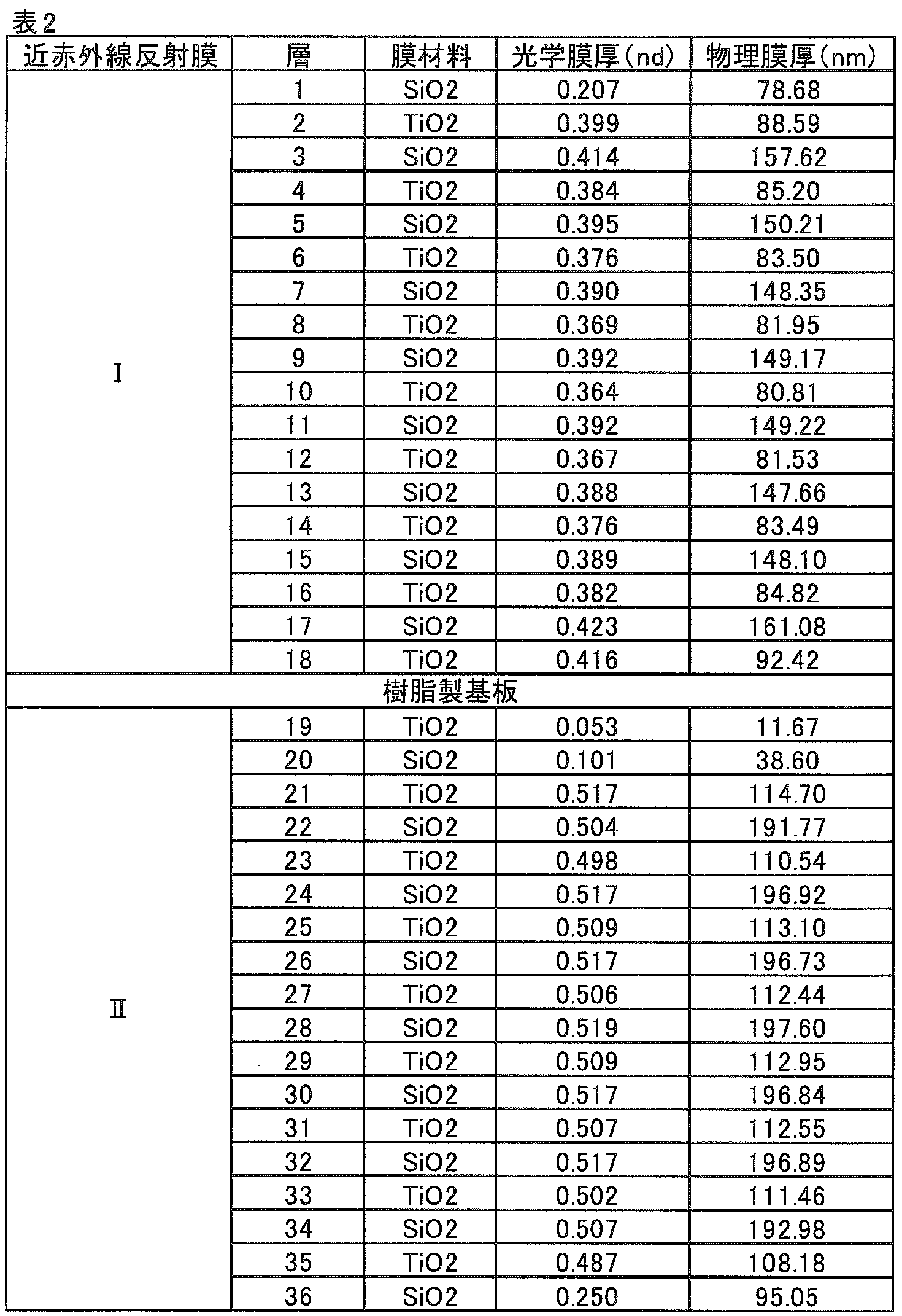
この光学フィルターの分光透過率および反射率を測定し、各波長領域における光学特性を評価した。結果を表7に示す。波長430~580nmにおける、光学フィルターの近赤外線反射膜(I)側から測定した透過率の平均値は87%であり、波長800~1200nmにおける、光学フィルターの近赤外線反射膜(I)側(A面)から測定した45°反射率の平均値は93%であり、5°反射率の平均値は97%であり、光学フィルターの近赤外線反射膜(II)側(B面)から測定した45°反射率の平均値は92%であり、5°反射率の平均値は97%であった。また、ゴースト光の発生は認められなかった。
[実施例2]
実施例1で得られた、厚さ0.1mm、縦60mm、横60mmの樹脂製基板の片面に近赤外線反射膜(III)を形成し、さらに樹脂製基板のもう一方の面に近赤外線反射膜(IV)を形成し、厚さ0.105mmの光学フィルターを得た。
実施例1で得られた、厚さ0.1mm、縦60mm、横60mmの樹脂製基板の片面に近赤外線反射膜(III)を形成し、さらに樹脂製基板のもう一方の面に近赤外線反射膜(IV)を形成し、厚さ0.105mmの光学フィルターを得た。
近赤外線反射膜(III)は、蒸着温度100℃で形成され、シリカ(SiO2)層と酸化チタン(TiO2)層とが交互に積層されてなる(合計26層)。近赤外線反射膜(IV)は、蒸着温度100℃で形成され、シリカ(SiO2)層と酸化チタン(TiO2)層とが交互に積層されてなる(合計20層)。
近赤外線反射膜(III)および(IV)の設計は、以下のようにして行った。
ソフトへの入力パラメーター(Target値、各層の層数、最終的に得られる光学フィルターの透過率および反射率)に基づき、実施例1と同様に最適化した結果、実施例2では、近赤外線反射膜(III)は、膜厚31~158nmのシリカ層と膜厚7~89nmの酸化チタン層とが交互に積層されてなる、積層数26の多層蒸着膜となり、近赤外線反射膜(IV)は、膜厚39~199nmのシリカ層と膜厚12~116nmの酸化チタン層とが交互に積層されてなる、積層数20の多層蒸着膜となった。最適化を行った膜構成の一例を表3に示す。
ソフトへの入力パラメーター(Target値、各層の層数、最終的に得られる光学フィルターの透過率および反射率)に基づき、実施例1と同様に最適化した結果、実施例2では、近赤外線反射膜(III)は、膜厚31~158nmのシリカ層と膜厚7~89nmの酸化チタン層とが交互に積層されてなる、積層数26の多層蒸着膜となり、近赤外線反射膜(IV)は、膜厚39~199nmのシリカ層と膜厚12~116nmの酸化チタン層とが交互に積層されてなる、積層数20の多層蒸着膜となった。最適化を行った膜構成の一例を表3に示す。
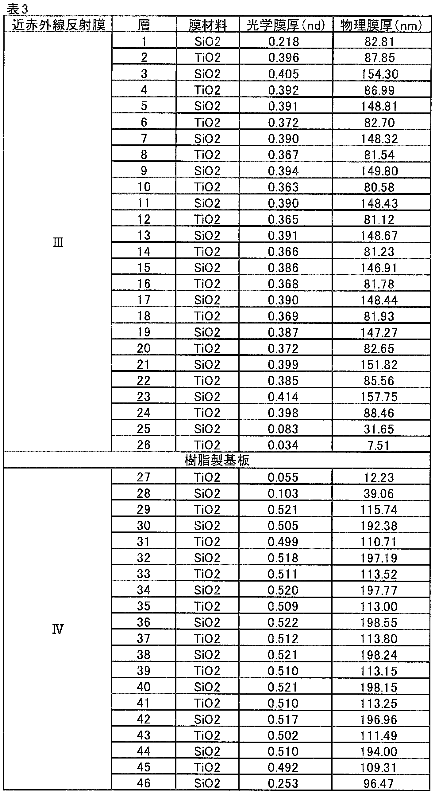
光学特性の評価結果を表7に示す。なお、本実施例においては、波長430~580nmにおける透過率は光学フィルターの近赤外線反射膜(III)側(A面)から、波長800~1200nmにおける反射率は光学フィルターの近赤外線反射膜(III)側(A面)および近赤外線反射膜(IV)側(B面)から測定した。
[実施例3]
実施例1で得られた、厚さ0.1mm、縦60mm、横60mmの樹脂製基板の片面に近赤外線反射膜(V)を形成し、厚さ0.105mmの光学フィルターを得た。
実施例1で得られた、厚さ0.1mm、縦60mm、横60mmの樹脂製基板の片面に近赤外線反射膜(V)を形成し、厚さ0.105mmの光学フィルターを得た。
近赤外線反射膜(V)は、蒸着温度100℃で形成され、シリカ(SiO2)層と酸化チタン(TiO2)層とが交互に積層されてなる(合計40層)。
近赤外線反射膜(V)の設計は、ソフトへの入力パラメーター(Target値)を下記表4の通りとし、また、各層の層数と、最終的に得られる光学フィルターの透過率および反射率(目標値;表7参照)とを入力パラメーターとして設定したこと以外は実施例1と同様に最適化し、膜厚36~193nmのシリカ層と膜厚10~113nmの酸化チタン層とが交互に積層されてなる、積層数40の多層蒸着膜となった。最適化を行った膜構成の一例を表5に示す。
近赤外線反射膜(V)の設計は、ソフトへの入力パラメーター(Target値)を下記表4の通りとし、また、各層の層数と、最終的に得られる光学フィルターの透過率および反射率(目標値;表7参照)とを入力パラメーターとして設定したこと以外は実施例1と同様に最適化し、膜厚36~193nmのシリカ層と膜厚10~113nmの酸化チタン層とが交互に積層されてなる、積層数40の多層蒸着膜となった。最適化を行った膜構成の一例を表5に示す。


[実施例4]~[実施例15]
表7に示す透明樹脂、近赤外線吸収色素、溶媒およびフィルム乾燥条件を採用して、実施例1と同様の手順にて樹脂製基板を製造し、さらにそれぞれ多層蒸着膜の各層の厚さについての最適化を行ったこと以外は実施例2と同様にして、厚さ0.106mmの光学フィルターを得た。結果を表7に示す。なお、表7において、溶液の樹脂濃度はいずれも20重量%である。
表7に示す透明樹脂、近赤外線吸収色素、溶媒およびフィルム乾燥条件を採用して、実施例1と同様の手順にて樹脂製基板を製造し、さらにそれぞれ多層蒸着膜の各層の厚さについての最適化を行ったこと以外は実施例2と同様にして、厚さ0.106mmの光学フィルターを得た。結果を表7に示す。なお、表7において、溶液の樹脂濃度はいずれも20重量%である。
[比較例1]
表7に示す透明樹脂、近赤外線吸収色素、溶媒およびフィルム乾燥条件を採用して、実施例1と同様の手順にて樹脂製基板からなる光学フィルターを製造した。結果を表7に示す。
表7に示す透明樹脂、近赤外線吸収色素、溶媒およびフィルム乾燥条件を採用して、実施例1と同様の手順にて樹脂製基板からなる光学フィルターを製造した。結果を表7に示す。
[比較例2]
比較例1で得られた、厚さ0.1mm、縦60mm、横60mmの樹脂製基板の片面に近赤外線反射膜(VI)を形成し、さらに樹脂製基板のもう一方の面に近赤外線反射膜(VII)を形成し、厚さ1.01mmの光学フィルターを得た。
比較例1で得られた、厚さ0.1mm、縦60mm、横60mmの樹脂製基板の片面に近赤外線反射膜(VI)を形成し、さらに樹脂製基板のもう一方の面に近赤外線反射膜(VII)を形成し、厚さ1.01mmの光学フィルターを得た。
近赤外線反射膜(VI)および(VII)は、実施例1のように光学薄膜設計ソフトを用いて最適化を行うのではなく、光学フィルターが表7記載の透過率および反射率を有するように特性を確認しながら膜厚および層数を設計した。近赤外線反射膜(VI)は、蒸着温度100℃で形成され、シリカ(SiO2)層と酸化チタン(TiO2)層とが交互に積層されてなる(合計6層)。近赤外線反射膜(VII)は、蒸着温度100℃で形成され、シリカ(SiO2)層と酸化チタン(TiO2)層とが交互に積層されてなる(合計4層)。
近赤外線反射膜(VI)は、膜厚74~155nmのシリカ層と膜厚83~87nmの酸化チタン層とが交互に積層されてなる、積層数6の多層蒸着膜となった。近赤外線反射膜(VII)は、膜厚79~164nmのシリカ層と膜厚89~94nmの酸化チタン層とが交互に積層されてなる、積層数4の多層蒸着膜となった。膜構成の一例を表6に示す。
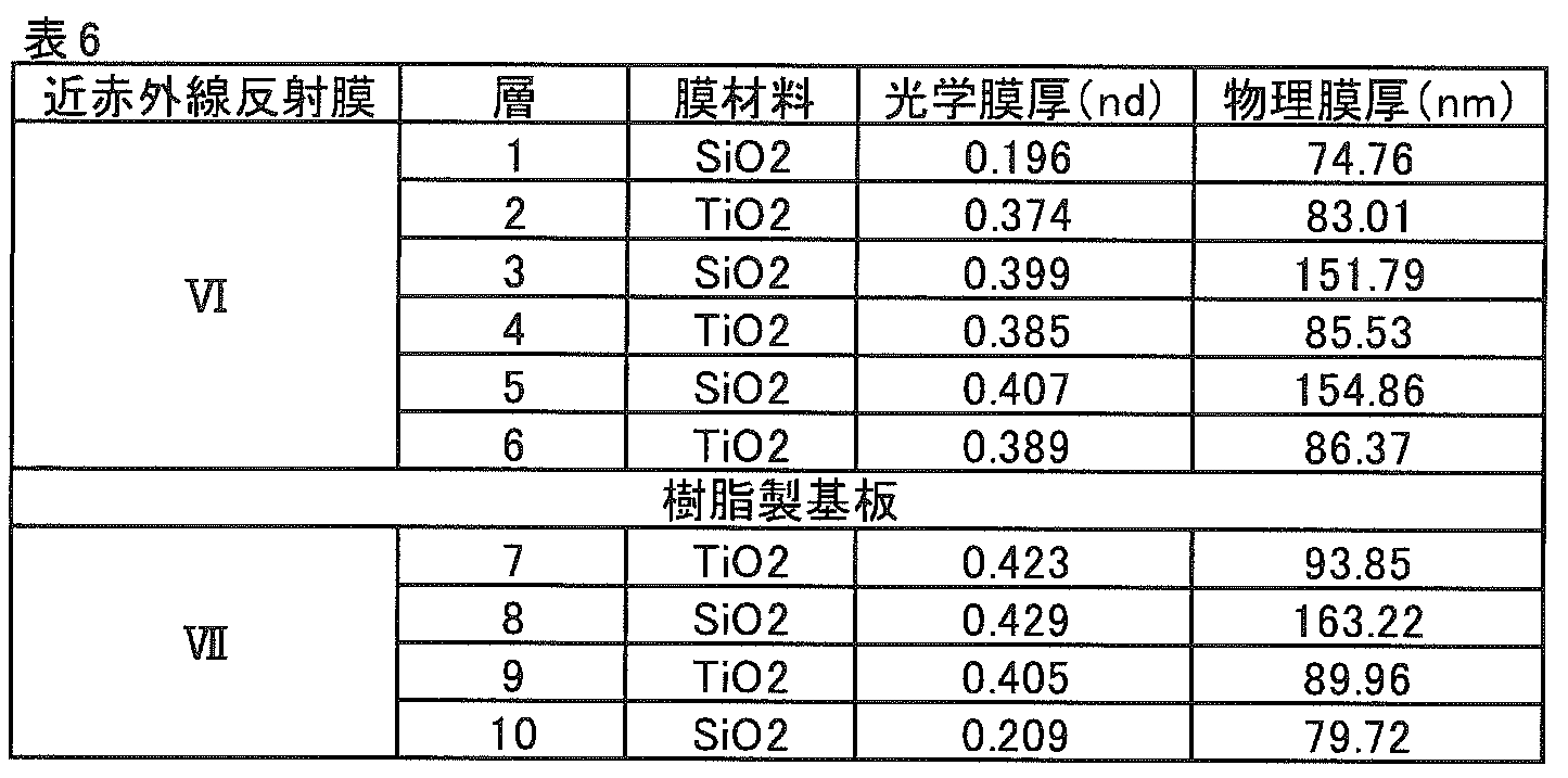
実施例および比較例で使用した各種化合物は以下のとおりである。
樹脂A:環状オレフィン系樹脂(樹脂合成例1)
樹脂B:芳香族ポリエーテル系樹脂(樹脂合成例2)
樹脂C:ポリイミド系樹脂(樹脂合成例3)
樹脂D:フルオレンポリカーボネート系樹脂(樹脂合成例4)
樹脂E:フルオレンポリエステル系樹脂(樹脂合成例5)
樹脂F:フッ素化ポリエーテルケトン(樹脂合成例6)
樹脂G:環状オレフィン系樹脂「ゼオノア 1420R」
(日本ゼオン(株)製)
樹脂H:環状オレフィン系樹脂「APEL #6015」
(三井化学(株)製)
樹脂I:ポリカーボネート系樹脂「ピュアエース」(帝人(株)製)
樹脂J:ポリエーテルサルホン系樹脂「スミライト FS-1300」
(住友ベークライト(株)製)
樹脂K:耐熱アクリル系樹脂「アクリビュア」((株)日本触媒製)
化合物(a-1):下記式(a-1)で表されるスクアリリウム系化合物
樹脂A:環状オレフィン系樹脂(樹脂合成例1)
樹脂B:芳香族ポリエーテル系樹脂(樹脂合成例2)
樹脂C:ポリイミド系樹脂(樹脂合成例3)
樹脂D:フルオレンポリカーボネート系樹脂(樹脂合成例4)
樹脂E:フルオレンポリエステル系樹脂(樹脂合成例5)
樹脂F:フッ素化ポリエーテルケトン(樹脂合成例6)
樹脂G:環状オレフィン系樹脂「ゼオノア 1420R」
(日本ゼオン(株)製)
樹脂H:環状オレフィン系樹脂「APEL #6015」
(三井化学(株)製)
樹脂I:ポリカーボネート系樹脂「ピュアエース」(帝人(株)製)
樹脂J:ポリエーテルサルホン系樹脂「スミライト FS-1300」
(住友ベークライト(株)製)
樹脂K:耐熱アクリル系樹脂「アクリビュア」((株)日本触媒製)
化合物(a-1):下記式(a-1)で表されるスクアリリウム系化合物

化合物(a-2):下記式(a-2)で表されるスクアリリウム系化合物

化合物(b-1):下記式(b-1)で表されるフタロシアニン系化合物
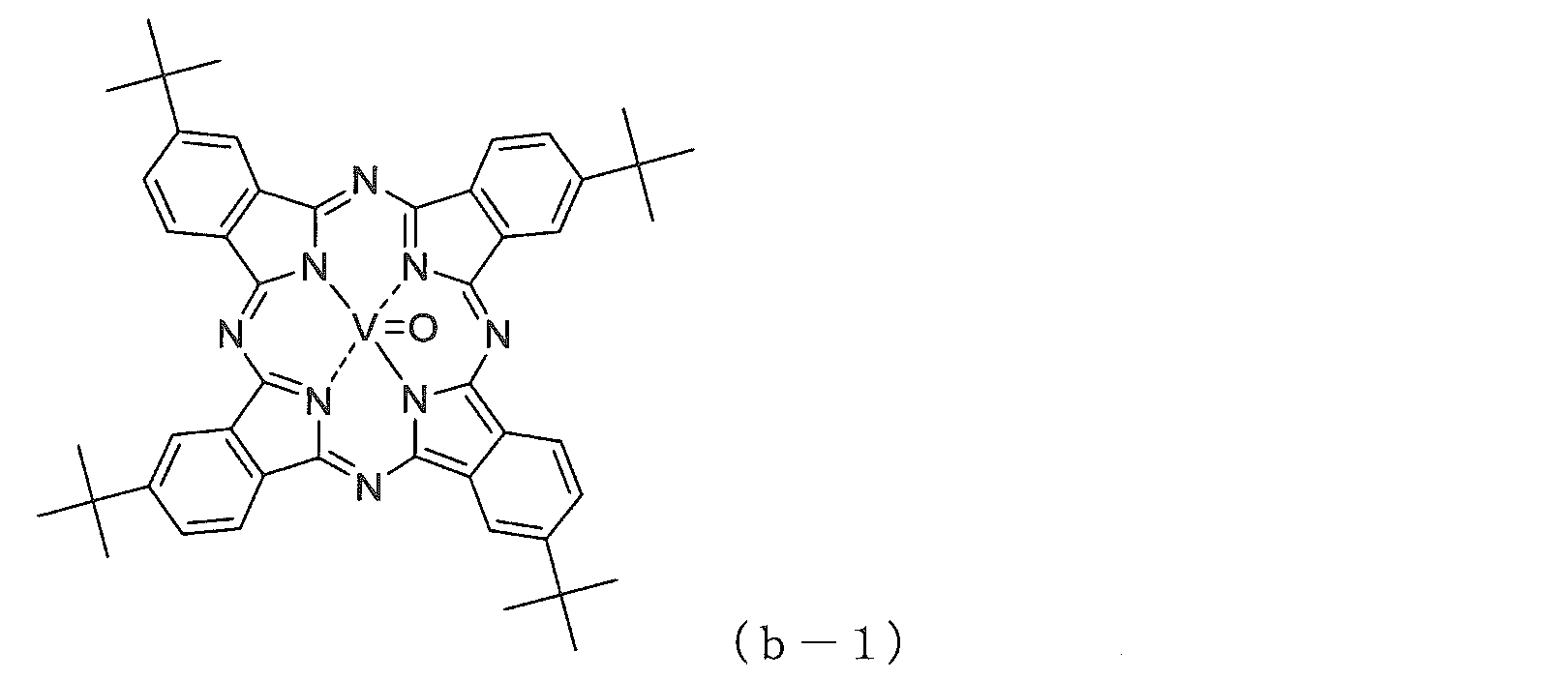
化合物(b-2):下記式(b-2)で表されるフタロシアニン系化合物
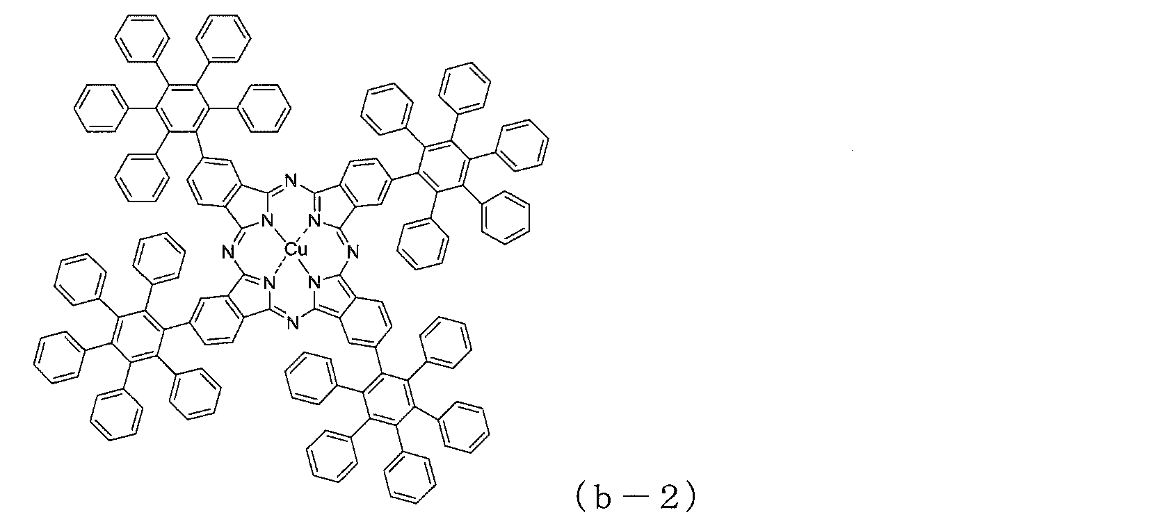
化合物(c-1):下記式(c-1)で表されるシアニン系化合物
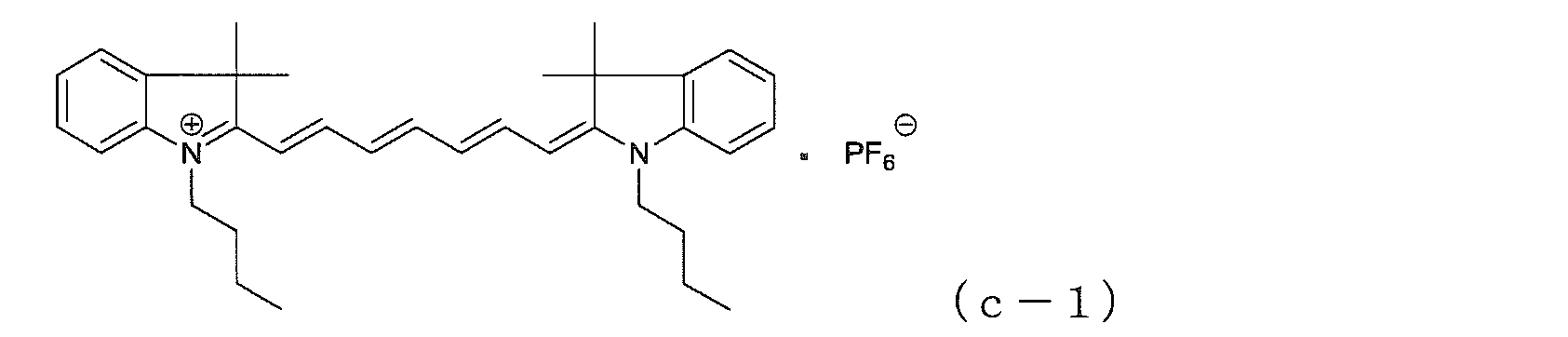
溶媒(1):塩化メチレン
溶媒(2):N,N-ジメチルアセトアミド
溶媒(3):酢酸エチル/トルエン(重量比:5/5)
溶媒(4):シクロヘキサン/キシレン(重量比:7/3)
溶媒(5):シクロヘキサン/塩化メチレン(重量比:99/1)
溶媒(6):N-メチル-2-ピロリドン
また、表7における、実施例および比較例のフィルム乾燥条件は以下の通りである。
溶媒(2):N,N-ジメチルアセトアミド
溶媒(3):酢酸エチル/トルエン(重量比:5/5)
溶媒(4):シクロヘキサン/キシレン(重量比:7/3)
溶媒(5):シクロヘキサン/塩化メチレン(重量比:99/1)
溶媒(6):N-メチル-2-ピロリドン
また、表7における、実施例および比較例のフィルム乾燥条件は以下の通りである。
条件(1):20℃/8hr→減圧下 100℃/8hr
条件(2):60℃/8hr→80℃/8hr→減圧下 140℃/8hr
条件(3):60℃/8hr→80℃/8hr→減圧下 100℃/24hr
条件(4):40℃/4hr→60℃/4hr→減圧下 100℃/8hr
なお、減圧乾燥前に、塗膜をガラス板から剥離した。
条件(2):60℃/8hr→80℃/8hr→減圧下 140℃/8hr
条件(3):60℃/8hr→80℃/8hr→減圧下 100℃/24hr
条件(4):40℃/4hr→60℃/4hr→減圧下 100℃/8hr
なお、減圧乾燥前に、塗膜をガラス板から剥離した。
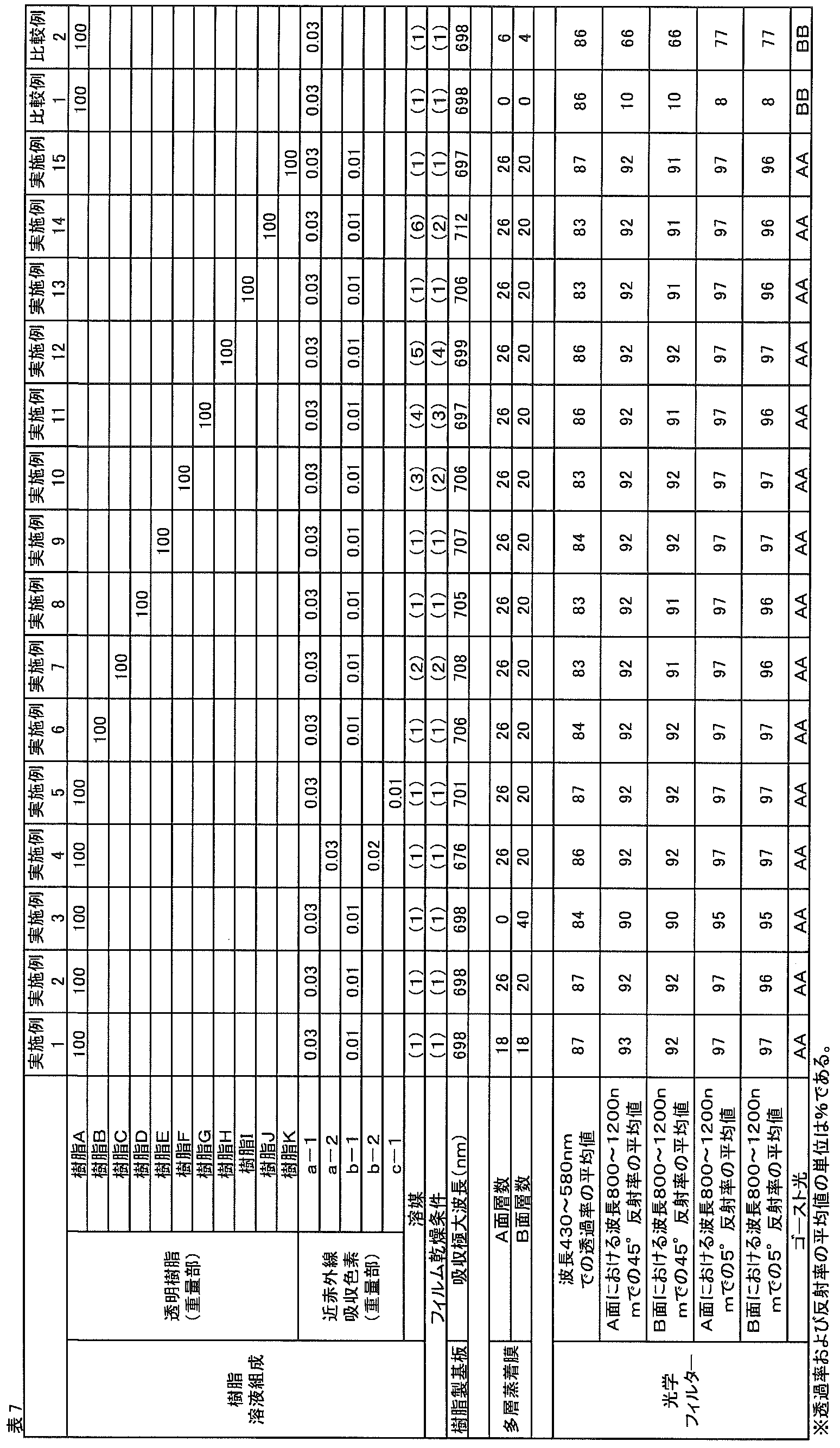
比較例2が示すように、5°反射率の平均値が70%以上であっても、45°反射率の平均値が70%未満であると、ゴースト光の発生が確認された。一方、各実施例が示すように、45°反射率の平均値が70%以上であると、ゴースト光の発生は確認されなかった。
したがって、本発明の上記要件を満たす光学フィルターは、可視光透過率や近赤外線カット特性に優れている上にゴースト光の発生を抑えることができ、固体撮像素子用途として要求される様々な特性を同時にバランスよく満たすことが出来る。このため、本発明の光学フィルターは、従来の光学フィルターと比べて特に固体撮像素子用途に好適に用いることが出来る。
1:光学フィルター
2:分光光度計
3:光
4:反射ミラー
2:分光光度計
3:光
4:反射ミラー
Claims (10)
- 透明樹脂製基板と、
前記基板の少なくとも一方の面上に形成された近赤外線反射膜とを有し、
下記(A)~(B)の要件を満たす光学フィルター:
(A)波長430~580nmの領域において、光学フィルターの垂直方向から測定した場合の透過率の平均値が75%以上。
(B)波長800~1200nmの領域において、光学フィルターの垂直方向に対して45°の角度で、光学フィルターの一方の面側から測定した場合の反射率の平均値が70%以上。 - 前記透明樹脂製基板を構成する透明樹脂が、環状オレフィン系樹脂、芳香族ポリエーテル系樹脂、ポリイミド系樹脂、フルオレンポリカーボネート系樹脂、フルオレンポリエステル系樹脂、ポリカーボネート系樹脂、ポリアミド系樹脂、ポリアリレート系樹脂、ポリサルホン系樹脂、ポリエーテルサルホン系樹脂、ポリパラフェニレン系樹脂、ポリアミドイミド系樹脂、ポリエチレンナフタレート系樹脂、フッ素化芳香族ポリマー系樹脂、(変性)アクリル系樹脂、エポキシ系樹脂、アリルエステル系樹脂およびシルセスキオキサン系樹脂からなる群より選ばれる少なくとも1種の樹脂である請求項1に記載の光学フィルター。
- 前記透明樹脂製基板が、近赤外線吸収色素を含有する請求項1または2に記載の光学フィルター。
- 前記透明樹脂製基板が、スクアリリウム系化合物、シアニン系化合物、フタロシアニン系化合物、ナフタロシアニン系化合物、クロコニウム系化合物、ジチオール系化合物、ジイモニウム系化合物およびポルフィリン系化合物からなる群より選ばれる少なくとも1種の近赤外線吸収色素を含有する請求項3に記載の光学フィルター。
- 前記近赤外線吸収色素が、式(I)で表されるスクアリリウム系化合物および式(II)で表されるスクアリリウム系化合物からなる群より選ばれる少なくとも1種を含む請求項3または4に記載の光学フィルター。

(i)複数あるRaは、それぞれ独立に水素原子、ハロゲン原子、スルホ基、水酸基、シアノ基、ニトロ基、カルボキシ基、リン酸基、-L1または-NReRf基を表し、ここでReおよびRfは、それぞれ独立に水素原子、-La、-Lb、-Lc、-Ldまたは-Leを表し;
複数あるRbは、それぞれ独立に水素原子、ハロゲン原子、スルホ基、水酸基、シアノ基、ニトロ基、カルボキシ基、リン酸基、-L1または-NRgRh基を表し、ここでRgおよびRhは、それぞれ独立に水素原子、-La、-Lb、-Lc、-Ld、-Leまたは-C(O)Ri基(Riは、-La、-Lb、-Lc、-Ldまたは-Leを表す。)を表し;
複数あるYは、それぞれ独立に-NRjRk基を表し、ここでRjおよびRkは、それぞれ独立に水素原子、-La、-Lb、-Lc、-Ldまたは-Leを表し;
L1は、La、Lb、Lc、Ld、Le、Lf、LgまたはLhであり;
前記La~Lhは、
(La)炭素数1~9の脂肪族炭化水素基、
(Lb)炭素数1~9のハロゲン置換アルキル基、
(Lc)炭素数3~14の脂環式炭化水素基、
(Ld)炭素数6~14の芳香族炭化水素基、
(Le)炭素数3~14の複素環基、
(Lf)炭素数1~9のアルコキシ基、
(Lg)炭素数1~9のアシル基、または
(Lh)炭素数1~9のアルコキシカルボニル基
を表し、前記La~Lhは、置換基Lを有していてもよく;
置換基Lは、炭素数1~9の脂肪族炭化水素基、炭素数1~9のハロゲン置換アルキル基、炭素数3~14の脂環式炭化水素基、炭素数6~14の芳香族炭化水素基および炭素数3~14の複素環基からなる群より選ばれる少なくとも1種であり;
前記La~Lhは、さらにハロゲン原子、スルホ基、水酸基、シアノ基、ニトロ基、カルボキシ基、リン酸基およびアミノ基からなる群より選ばれる少なくとも1種の原子または基を有していてもよく;
(ii)1つのベンゼン環上の2つのRaのうちの少なくとも1つが、同じベンゼン環上のYと相互に結合して、窒素原子を少なくとも1つ含む構成原子数5または6の複素環を形成し、前記複素環は置換基を有していてもよく、Rbおよび前記複素環の形成に関与しないRaは、それぞれ独立に前記(i)のRbおよびRaと同義である。]

- 波長800~1200nmの領域において、光学フィルターの垂直方向に対して45°の角度から測定した場合の反射率の平均値が、光学フィルターのいずれの面側から測定した場合においても70%以上である請求項1~5のいずれか1項に記載の光学フィルター。
- 前記透明樹脂製基板と、
前記基板の両面上に形成された前記近赤外線反射膜と
を有する請求項1~6のいずれか1項に記載の光学フィルター。 - 固体撮像装置用である請求項1~7のいずれか1項に記載の光学フィルター。
- 請求項1~7のいずれか1項に記載の光学フィルターを具備する固体撮像装置。
- 請求項1~7のいずれか1項に記載の光学フィルターを具備するカメラモジュール。
Applications Claiming Priority (2)
| Application Number | Priority Date | Filing Date | Title |
|---|---|---|---|
| JP2013168107 | 2013-08-13 | ||
| JP2013-168107 | 2013-08-13 |
Publications (1)
| Publication Number | Publication Date |
|---|---|
| WO2015022892A1 true WO2015022892A1 (ja) | 2015-02-19 |
Family
ID=52468279
Family Applications (1)
| Application Number | Title | Priority Date | Filing Date |
|---|---|---|---|
| PCT/JP2014/070706 Ceased WO2015022892A1 (ja) | 2013-08-13 | 2014-08-06 | 光学フィルターおよび前記フィルターを用いた装置 |
Country Status (2)
| Country | Link |
|---|---|
| TW (1) | TW201506463A (ja) |
| WO (1) | WO2015022892A1 (ja) |
Cited By (9)
| Publication number | Priority date | Publication date | Assignee | Title |
|---|---|---|---|---|
| JP2017129791A (ja) * | 2016-01-21 | 2017-07-27 | 株式会社日本触媒 | 光選択透過フィルターおよびその製造方法 |
| CN109313296A (zh) * | 2016-06-08 | 2019-02-05 | Jsr株式会社 | 光学滤波器及光学传感装置 |
| US10228500B2 (en) | 2015-04-23 | 2019-03-12 | AGC Inc. | Optical filter and imaging device |
| US10310150B2 (en) | 2015-01-14 | 2019-06-04 | AGC Inc. | Near-infrared cut filter and solid-state imaging device |
| US10351718B2 (en) | 2015-02-18 | 2019-07-16 | AGC Inc. | Optical filter and imaging device |
| US10365417B2 (en) | 2015-01-14 | 2019-07-30 | AGC Inc. | Near-infrared cut filter and imaging device |
| US10598834B2 (en) | 2015-12-01 | 2020-03-24 | AGC Inc. | Near-infrared light blocking optical filter having high visible light transmission and an imaging device using the optical filter |
| JPWO2020204025A1 (ja) * | 2019-04-03 | 2020-10-08 | ||
| US11059977B2 (en) | 2016-02-02 | 2021-07-13 | AGC Inc. | Near-infrared-absorbing dye, optical filter, and imaging device |
Families Citing this family (4)
| Publication number | Priority date | Publication date | Assignee | Title |
|---|---|---|---|---|
| CN107407754B (zh) * | 2015-03-27 | 2020-02-07 | Jsr株式会社 | 光学滤波器及使用光学滤波器的装置 |
| JP7630759B2 (ja) * | 2020-02-21 | 2025-02-18 | Jsr株式会社 | 樹脂組成物、化合物(Z)、基材(i)、光学フィルターおよびその用途 |
| EP4123726B1 (en) * | 2020-03-16 | 2024-12-04 | Nitto Denko Corporation | Optical filter, method for manufacturing same, and optical module |
| CN115298580A (zh) * | 2020-03-16 | 2022-11-04 | 日东电工株式会社 | 滤光器、其制造方法及光学模块 |
Citations (4)
| Publication number | Priority date | Publication date | Assignee | Title |
|---|---|---|---|---|
| JP2012008532A (ja) * | 2010-05-26 | 2012-01-12 | Jsr Corp | 近赤外線カットフィルターおよび近赤外線カットフィルターを用いた装置 |
| WO2012169447A1 (ja) * | 2011-06-06 | 2012-12-13 | 旭硝子株式会社 | 光学フィルタ、固体撮像素子、撮像装置用レンズおよび撮像装置 |
| WO2013038938A1 (ja) * | 2011-09-15 | 2013-03-21 | Jsr株式会社 | 近赤外線カットフィルターおよび近赤外線カットフィルターを用いた装置 |
| WO2013054864A1 (ja) * | 2011-10-14 | 2013-04-18 | Jsr株式会社 | 光学フィルターならびに該光学フィルターを用いた固体撮像装置およびカメラモジュール |
-
2014
- 2014-08-06 WO PCT/JP2014/070706 patent/WO2015022892A1/ja not_active Ceased
- 2014-08-11 TW TW103127407A patent/TW201506463A/zh unknown
Patent Citations (4)
| Publication number | Priority date | Publication date | Assignee | Title |
|---|---|---|---|---|
| JP2012008532A (ja) * | 2010-05-26 | 2012-01-12 | Jsr Corp | 近赤外線カットフィルターおよび近赤外線カットフィルターを用いた装置 |
| WO2012169447A1 (ja) * | 2011-06-06 | 2012-12-13 | 旭硝子株式会社 | 光学フィルタ、固体撮像素子、撮像装置用レンズおよび撮像装置 |
| WO2013038938A1 (ja) * | 2011-09-15 | 2013-03-21 | Jsr株式会社 | 近赤外線カットフィルターおよび近赤外線カットフィルターを用いた装置 |
| WO2013054864A1 (ja) * | 2011-10-14 | 2013-04-18 | Jsr株式会社 | 光学フィルターならびに該光学フィルターを用いた固体撮像装置およびカメラモジュール |
Cited By (13)
| Publication number | Priority date | Publication date | Assignee | Title |
|---|---|---|---|---|
| US10365417B2 (en) | 2015-01-14 | 2019-07-30 | AGC Inc. | Near-infrared cut filter and imaging device |
| US10310150B2 (en) | 2015-01-14 | 2019-06-04 | AGC Inc. | Near-infrared cut filter and solid-state imaging device |
| US10745572B2 (en) | 2015-02-18 | 2020-08-18 | AGC Inc. | Squarylium-based dye for near-infrared optical filter |
| US10351718B2 (en) | 2015-02-18 | 2019-07-16 | AGC Inc. | Optical filter and imaging device |
| US10228500B2 (en) | 2015-04-23 | 2019-03-12 | AGC Inc. | Optical filter and imaging device |
| US10598834B2 (en) | 2015-12-01 | 2020-03-24 | AGC Inc. | Near-infrared light blocking optical filter having high visible light transmission and an imaging device using the optical filter |
| JP2017129791A (ja) * | 2016-01-21 | 2017-07-27 | 株式会社日本触媒 | 光選択透過フィルターおよびその製造方法 |
| US11059977B2 (en) | 2016-02-02 | 2021-07-13 | AGC Inc. | Near-infrared-absorbing dye, optical filter, and imaging device |
| CN109313296A (zh) * | 2016-06-08 | 2019-02-05 | Jsr株式会社 | 光学滤波器及光学传感装置 |
| CN109313296B (zh) * | 2016-06-08 | 2021-05-11 | Jsr株式会社 | 光学滤波器及光学传感装置 |
| JPWO2020204025A1 (ja) * | 2019-04-03 | 2020-10-08 | ||
| WO2020204025A1 (ja) * | 2019-04-03 | 2020-10-08 | Agc株式会社 | 光学フィルタおよび撮像装置 |
| JP7342944B2 (ja) | 2019-04-03 | 2023-09-12 | Agc株式会社 | 光学フィルタおよび撮像装置 |
Also Published As
| Publication number | Publication date |
|---|---|
| TW201506463A (zh) | 2015-02-16 |
Similar Documents
| Publication | Publication Date | Title |
|---|---|---|
| JP6380390B2 (ja) | 光学フィルターおよび前記フィルターを用いた装置 | |
| JP6627864B2 (ja) | 光学フィルターおよび光学フィルターを用いた装置 | |
| JP6331392B2 (ja) | 光学フィルターならびに該光学フィルターを用いた固体撮像装置およびカメラモジュール | |
| JP6256335B2 (ja) | 固体撮像素子用光学フィルターおよびその用途 | |
| JP6358114B2 (ja) | 光学フィルターおよび光学フィルターを用いた装置 | |
| WO2015022892A1 (ja) | 光学フィルターおよび前記フィルターを用いた装置 | |
| JP5884953B2 (ja) | 光学フィルター、固体撮像装置およびカメラモジュール | |
| JP2021039369A (ja) | 光学フィルターおよび光学フィルターを用いた装置 | |
| WO2014192715A1 (ja) | 光学フィルターおよび前記フィルターを用いた装置 | |
| JP6578718B2 (ja) | 光学フィルターおよび光学フィルターを用いた装置 | |
| JPWO2019022069A1 (ja) | 近赤外線カットフィルターおよび該近赤外線カットフィルターを用いた装置 | |
| WO2018043564A1 (ja) | 光学フィルターおよび光学フィルターを用いた装置 | |
| JP6398980B2 (ja) | 光学フィルターおよび光学フィルターを用いた装置 | |
| JP2015040895A (ja) | 光学フィルターおよび光学フィルターを用いた装置 | |
| JP6693585B2 (ja) | 光学フィルターおよび光学フィルターを用いた装置 | |
| JP2021120733A (ja) | 光学フィルターおよびその用途 |
Legal Events
| Date | Code | Title | Description |
|---|---|---|---|
| 121 | Ep: the epo has been informed by wipo that ep was designated in this application |
Ref document number: 14836133 Country of ref document: EP Kind code of ref document: A1 |
|
| NENP | Non-entry into the national phase |
Ref country code: DE |
|
| 122 | Ep: pct application non-entry in european phase |
Ref document number: 14836133 Country of ref document: EP Kind code of ref document: A1 |
|
| NENP | Non-entry into the national phase |
Ref country code: JP |