WO2015019607A1 - 異方性導電体膜とその製造方法、デバイス、電子放出素子、フィールドエミッションランプ、及びフィールドエミッションディスプレイ - Google Patents
異方性導電体膜とその製造方法、デバイス、電子放出素子、フィールドエミッションランプ、及びフィールドエミッションディスプレイ Download PDFInfo
- Publication number
- WO2015019607A1 WO2015019607A1 PCT/JP2014/004089 JP2014004089W WO2015019607A1 WO 2015019607 A1 WO2015019607 A1 WO 2015019607A1 JP 2014004089 W JP2014004089 W JP 2014004089W WO 2015019607 A1 WO2015019607 A1 WO 2015019607A1
- Authority
- WO
- WIPO (PCT)
- Prior art keywords
- conductor
- film
- hole
- conductor film
- metal
- Prior art date
- Legal status (The legal status is an assumption and is not a legal conclusion. Google has not performed a legal analysis and makes no representation as to the accuracy of the status listed.)
- Ceased
Links
Images




Classifications
-
- H—ELECTRICITY
- H01—ELECTRIC ELEMENTS
- H01J—ELECTRIC DISCHARGE TUBES OR DISCHARGE LAMPS
- H01J1/00—Details of electrodes, of magnetic control means, of screens, or of the mounting or spacing thereof, common to two or more basic types of discharge tubes or lamps
- H01J1/02—Main electrodes
- H01J1/30—Cold cathodes, e.g. field-emissive cathode
- H01J1/304—Field-emissive cathodes
-
- H—ELECTRICITY
- H01—ELECTRIC ELEMENTS
- H01J—ELECTRIC DISCHARGE TUBES OR DISCHARGE LAMPS
- H01J31/00—Cathode ray tubes; Electron beam tubes
- H01J31/08—Cathode ray tubes; Electron beam tubes having a screen on or from which an image or pattern is formed, picked up, converted, or stored
- H01J31/10—Image or pattern display tubes, i.e. having electrical input and optical output; Flying-spot tubes for scanning purposes
- H01J31/12—Image or pattern display tubes, i.e. having electrical input and optical output; Flying-spot tubes for scanning purposes with luminescent screen
- H01J31/123—Flat display tubes
- H01J31/125—Flat display tubes provided with control means permitting the electron beam to reach selected parts of the screen, e.g. digital selection
- H01J31/127—Flat display tubes provided with control means permitting the electron beam to reach selected parts of the screen, e.g. digital selection using large area or array sources, i.e. essentially a source for each pixel group
-
- H—ELECTRICITY
- H01—ELECTRIC ELEMENTS
- H01J—ELECTRIC DISCHARGE TUBES OR DISCHARGE LAMPS
- H01J63/00—Cathode-ray or electron-stream lamps
- H01J63/02—Details, e.g. electrode, gas filling, shape of vessel
-
- H—ELECTRICITY
- H01—ELECTRIC ELEMENTS
- H01J—ELECTRIC DISCHARGE TUBES OR DISCHARGE LAMPS
- H01J63/00—Cathode-ray or electron-stream lamps
- H01J63/06—Lamps with luminescent screen excited by the ray or stream
-
- H—ELECTRICITY
- H01—ELECTRIC ELEMENTS
- H01J—ELECTRIC DISCHARGE TUBES OR DISCHARGE LAMPS
- H01J9/00—Apparatus or processes specially adapted for the manufacture, installation, removal, maintenance of electric discharge tubes, discharge lamps, or parts thereof; Recovery of material from discharge tubes or lamps
- H01J9/02—Manufacture of electrodes or electrode systems
- H01J9/022—Manufacture of electrodes or electrode systems of cold cathodes
- H01J9/025—Manufacture of electrodes or electrode systems of cold cathodes of field emission cathodes
Definitions
- the present invention relates to an anisotropic conductor film, a manufacturing method thereof, and a device / electron emitting element / field emission lamp / field emission display using the anisotropic conductor film.
- Field emission (FE) devices are expected to provide high brightness with low power consumption.
- the FE device can be used as a field emission lamp (Field Emission Lump: FEL) or a field emission display (Field Emission Display: FED).
- FEL Field Emission lamp
- FED Field Emission Display
- the phosphor layer provided on the anode substrate is excited by the electron beam emitted from the emitter (electron source) provided on the cathode substrate, and light emission is obtained.
- the emitter electron source
- spindt emitters, carbon nanotube (CNT) emitters, and the like are used as emitters.
- the Spindt-type emitter has a complicated manufacturing process and it is difficult to increase the area. It is difficult to design a structure of a CNT emitter in which CNTs having high crystallinity are regularly arranged with a uniform length.
- An anodized metal film having a plurality of needle-like non-through holes and a barrier layer can be obtained by anodizing at least a part of an anodized metal body such as Al.
- anodized metal body such as Al.
- a conductor film can be formed on one surface of the pore structure, and a needle-like conductor can be formed inside the plurality of through holes by electrolytic plating.
- a high electric field can be locally generated in the electric field at the tip of the conductor formed inside the through hole.
- Non-Patent Document 1 proposes use of the above structure for an FE device.
- Patent Document 1 discloses a structure in which a Spindt-type emitter is further formed on a conductor formed inside a plurality of through holes in the structure (FIG. 1).
- a plurality of emitter layers arranged in the plane direction on the electrode layer are referred to as “emitter layers”.
- An element including an electrode layer and an emitter layer is referred to as an “electron emitting element”.
- Patent Document 2 discloses a configuration in which a through hole is provided in a CNT emitter layer (FIG. 1).
- the diameter (W) of the through hole is fixed to 80 ⁇ m, the pattern width (S) of the CNT emitter layer is reduced to relatively increase the space, thereby improving the electron emission performance. (FIG. 7).
- the diameter of through holes is, for example, about 20 to 200 nm, and the interval between adjacent through holes is, for example, about 20 to 200 nm. Therefore, in the electron-emitting device using the anodized metal film proposed in Non-Patent Document 1 and Patent Document 1, the emitter gap is very narrow throughout the device, and it is difficult to obtain high electron-emitting performance.
- Patent Document 3 discloses that an anodized metal body is anodized, and a part of a plurality of non-through holes of the obtained anodized metal film is selectively formed as a through hole.
- a microelectrode array in which a conductor is selectively formed is described (claims 1, 2, and 2).
- anodization is performed after a plurality of depressions are provided on the surface by pressing a SiC mold against an anodized metal body (Al).
- Al anodized metal body
- the non-through hole of the part where the dent is not formed is selectively made a through hole, and a needle-like conductor is selectively formed inside it. can do.
- this method is complicated in process.
- it is necessary to remove the barrier layer where the depression is not formed while leaving the barrier layer where the depression is formed, and it is difficult to control the removal of the barrier layer.
- the surface of the metal to be anodized (Al) has fine irregularities and the flatness is low, the depression cannot be provided even if the SiC mold is pressed.
- irregularities of several ⁇ m or more, such as rolling streaks often occur. Therefore, it is difficult to increase the area from the point of flatness of the anodized metal body (Al).
- Patent Document 4 after obtaining an anodized metal film having a plurality of through-holes in a semiconductor chip application, a resist pattern is formed on the surface, and some through-holes are selected using this resist pattern as a mask.
- a method of manufacturing an anisotropic conductive film is described in which the diameter of the conductive film is increased and the conductive material is selectively formed in the expanded through hole (FIGS. 3A to 3E). Since the anodized metal film has hydrophilicity and the resist has lipophilicity, it is not easy to apply the resist directly on the surface of the anodized metal film. In order to carry out the method described in Patent Document 4, at least a hydrophobizing agent is required.
- Patent Document 4 is difficult to implement in the first place.
- the tip of the conductor formed in the through hole is contaminated or altered by a hydrophobizing agent, a resist, or a solvent used for removing the resist pattern, and the performance as an emitter is lowered.
- the performance as an emitter is lowered.
- the entire emitter may be contaminated by heat diffusion due to the heating process, and the performance as the emitter may be deteriorated.
- the present invention has been made in view of the above circumstances, and is selectively formed in a pore structure made of an anodized metal film having a plurality of through holes and inside some of the plurality of through holes. It is an object of the present invention to provide an anisotropic conductive film that can be manufactured without using a resist without requiring complicated process control and a method for manufacturing the same.
- the anisotropic conductor film of the present invention is A pore structure composed of an anodized metal film having a plurality of through-holes extending in a direction intersecting with the surface direction, and a conductive material selectively formed inside some of the plurality of through-holes With body, further, One surface of the pore structure covers the opening of the through-hole in which the conductor is formed, and can be plated with the material of the conductor; A second conductor film that covers the opening of the through hole in which no body is formed, is connected to the first conductor film, and is difficult to plate the material of the conductor. .
- the method for producing an anisotropic conductive film of the present invention comprises: A pore structure composed of an anodized metal film having a plurality of through-holes extending in a direction intersecting with the surface direction, and a conductive material selectively formed inside some of the plurality of through-holes A method for producing an anisotropic conductive film comprising a body, Preparing the pore structure (A); One surface of the pore structure covers the opening of the through-hole in which the conductor is formed, and can be plated with the material of the conductor; A step (B) of forming a second conductor film that covers the opening of the through-hole where no body is formed and is connected to the first conductor film and is difficult to plate the material of the conductor; , Step (C) of performing electroplating on the pore structure using the first conductor film and the second conductor film as electrode layers in sequence.
- the device of the present invention includes the anisotropic conductive film of the present invention described above.
- the electron-emitting device of the present invention is Comprising the above anisotropic conductive film of the present invention, An electrode layer including the first conductor film and the second conductor film, and an electron source made of the conductor formed in the through hole.
- the field emission lamp (FEL) of the present invention is A first electrode substrate including the electron-emitting device of the present invention, A second electrode substrate including an electrode layer and a phosphor layer is disposed opposite to the first electrode substrate via a vacuum space.
- the field emission display (FED) of the present invention is A first electrode substrate including the electron-emitting device of the present invention, A second electrode substrate disposed opposite to the first electrode substrate via a vacuum space and including an electrode layer and a phosphor layer; Display is performed by modulation of light emitted from the phosphor layer.
- an anisotropic conductive film that can be manufactured without using a resist without requiring complicated process control and a method for manufacturing the same can be provided.
- FIG. 1B is a schematic plan view of the anisotropic conductive film of FIG. 1A.
- FIG. It is process drawing which shows the manufacturing method of the anisotropic conductor film of FIG. 1A. It is process drawing which shows the manufacturing method of the anisotropic conductor film of FIG. 1A. It is process drawing which shows the manufacturing method of the anisotropic conductor film of FIG. 1A. It is process drawing which shows the manufacturing method of the anisotropic conductor film of FIG. 1A. It is process drawing which shows the manufacturing method of the anisotropic conductor film of FIG. 1A. It is process drawing which shows the manufacturing method of the anisotropic conductor film of FIG. 1A.
- 2 is a SEM surface photograph of the anisotropic conductive film obtained in Example 1.
- 6 is a SEM surface photograph of the anisotropic conductive film obtained in Example 5.
- 6 is a SEM surface photograph of an anisotropic conductor film obtained in Example 6.
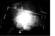
- 2 is a light emission photograph of FEL using the anisotropic conductive film obtained in Example 1.
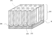
- FIG. 1A is a schematic cross-sectional view of the anisotropic conductive film of this embodiment.
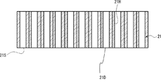
- FIG. 1B is a schematic plan view of the anisotropic conductive film of the present embodiment, and is a view showing a planar pattern of the through holes 21H and the conductors 22.
- the anisotropic conductive film 1 of this embodiment can be preferably used for an electron-emitting device used for a field emission (FE) device or the like.
- the FE device has a first electrode substrate including an electron-emitting device including an electrode layer and an emitter (electron source), and is opposed to the first electrode substrate through a vacuum space.
- the device includes a second electrode substrate that is disposed and includes an electrode layer and a phosphor layer.
- the anisotropic conductor film 1 of the present embodiment is a pore structure formed of an anodized metal film having a plurality of needle-like through-holes 21H extending in a direction crossing the plane direction. 21 is provided.
- a conductor 22 is selectively formed inside some of the through holes 21H among the plurality of through holes 21H.
- reference numeral 21S denotes one surface (lower surface in the drawing) of the pore structure 21
- reference numeral 21D denotes an opening of the through hole 21H in the surface 21S.
- a conductor film 30 composed of a first conductor film 31 and a second conductor film 32 is formed on the surface 21 ⁇ / b> S of the pore structure 21.
- a first conductor film 31 that covers the opening 21D of the through hole 21H in which the conductor 22 is formed and can be plated with the material of the conductor 22, and the inside
- a second conductor film 32 is formed which covers the opening 21D of the through hole 21H where the conductor 22 is not formed, is connected to the first conductor film 31, and is difficult to plate the material of the conductor 22.
- the first conductor film 31 covers the opening 21D of the through hole 21H in which the conductor 22 is formed, and the opening 21D of the through hole 21H in which the conductor 22 is not formed. In a pattern that does not cover the film, it is divided into a plurality of regions.
- the second conductor film 32 covers the opening 21D of the through hole 21H in which the conductor 22 is not formed, and is a pattern unit of the first conductor film 31 formed in a plurality of regions. It is formed to connect each other.
- the second conductor film 32 is a solid film having no pattern.
- the first conductor film 31 and the second conductor film 32 are formed so as to be connected to each other in order to integrally form the electrode layer.
- a plurality of pattern units of the first conductor film 31 that are spaced apart from each other can be conducted through the second conductor film 32.
- the pattern unit 31 ⁇ / b> P of the first conductor film 31 has a substantially rectangular pattern including 2 ⁇ 2 through holes 21 ⁇ / b> H in which conductors 22 are formed. It is. Between the pattern units 31P of the first conductor films 31 adjacent to each other in plan view, there are 2 ⁇ 2 through holes 21H in which the conductor 22 is not formed. As described above, the second conductor film 32 is formed immediately below the through hole 21H in which the conductor 22 is not formed. Note that the pattern design is merely an example, and it is possible to freely design which of the plurality of through holes 21H the conductor 22 is formed in. In the present embodiment, by changing the pattern of the first conductor film 31, the through hole 21H in which the conductor 22 is formed can be freely selected.
- the conductor 22 formed inside the through hole 21H is made of a material that can be electrolytically plated.
- the conductor 22 preferably contains a metal or a metal compound containing at least one metal element selected from the group consisting of Ag, Au, Cd, Co, Cu, Fe, Mo, Ni, Sn, W, and Zn. .
- a metal or a metal compound containing Ni and / or Ag is particularly preferable from the viewpoint of easy production and high conductivity.
- a metal or a metal compound containing Mo and / or W is particularly preferable from the viewpoint of a high melting point.
- the metal may be a single metal or an alloy. Examples of the metal compound include metal oxides.
- the first conductor film 31 is made of a material capable of plating the material of the conductor 22.
- the first conductor film 31 preferably contains a metal or metal compound containing at least one metal element selected from the group consisting of Au, Ag, Cu, Fe, Ni, Sn, and Zn.
- a metal or a metal compound containing Au and / or Ag is particularly preferable from the viewpoint of a high standard electrode potential.
- the metal may be a single metal or an alloy. Examples of the metal compound include metal oxides.
- the second conductor film 32 is made of a material that is difficult to plate the material of the conductor 22 (a difficult plating material).
- the difficult plating material include a metal or a metal compound in which an oxide film having a high insulating property is likely to be generated on the surface.
- the second conductor film 32 preferably contains a metal or metal compound containing at least one metal element selected from the group consisting of Al, Mg, Si, Ti, Mo, and W, or stainless steel. Among these, a metal or a metal compound containing Al is particularly preferable from the viewpoint of easy production and low cost.
- the metal may be a single metal or an alloy. Examples of the metal compound include metal oxides. Examples of stainless steel include Fe—Ni—Cr alloy.
- the anisotropic conductive film 1 of this embodiment can be used as an electron-emitting device used for an FE device or the like.
- the conductor film 30 composed of the first conductor film 31 and the second conductor film 32 is an electrode layer, and the conductor 22 formed inside the through hole 21H is an emitter (electron source). Each can be used.
- the preferred size design of the conductor 22 and the through hole 21H in the electron-emitting device is as follows.
- the length of the conductor 22 is preferably 1 ⁇ m or more, and particularly preferably 5 ⁇ m or more.
- the diameter of the conductor 22 is preferably 500 nm or less, more preferably 100 nm or less, and particularly preferably 50 nm or less. Considering the ease of formation, the diameter of the conductor 22 is preferably 20 nm or more. Since the electron emission performance is improved, the length / diameter of the conductor 22 is preferably 100 or more.
- the conductor 22 is formed inside the through hole 21H.
- the length of the through hole 21H is preferably 1 ⁇ m or more, and particularly preferably 5 ⁇ m or more.
- the diameter of the through hole 21H is preferably 500 nm or less, more preferably 100 nm or less, and particularly preferably 50 nm or less.
- the length / diameter of the through hole 21H is preferably 100 or more.
- the filling rate of the conductor 22 in the through hole 21H in which the conductor 22 is formed is 100% is illustrated.
- the filling rate of the conductor 22 is not 100%. Also good.
- the filling rate of the conductor 22 in the through hole 21H in which the conductor 22 is formed is preferably as high as possible, and is preferably 70 to 100%.
- the filling rate of the conductor 22 inside the through hole 21H is defined by the length of the conductor 22 / the length of the through hole 21H ⁇ 100 (%).
- the filling rate of the conductor 22 in each through hole 21H is preferably 70 to 100%.
- the filling rate of the conductor 22 in the through hole 21H in which the conductor 22 is formed may vary, but in this case, in-plane variation of the electron emission performance occurs. Considering the in-plane uniformity of the electron emission performance, it is preferable that the variation in the filling rate is small.
- the length of the through hole 21H is determined in consideration of a preferable length of the conductor 22 and a filling rate of the conductor 22 inside the through hole 21H.
- the conductors 22 formed inside the plurality of through holes 21H formed immediately above one pattern unit 31P of the first conductor film 31 constitute one conductor group 22G. ing.
- the plurality of conductor groups 22G are separated from each other via a plurality of through holes 21H in which the conductors 22 are not formed.
- the plurality of conductor groups 22G are separated from each other, and the control of the intervals is easy.
- the anisotropic conductive film 1 of this embodiment is used for a device such as an FE device, the emitter gap can be controlled over a wide range.
- the emitter gap in this embodiment, the gap between adjacent conductor groups 22G
- the emitter gap can be controlled in the range of about 100 nm to several tens of ⁇ m.
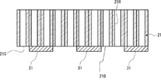
- FIG. 3 is a schematic cross-sectional view showing a design change example of the anisotropic conductive film.
- the same constituent elements as those of the anisotropic conductive film 1 of the above embodiment are denoted by the same reference numerals.
- the second conductor film 32 covers the opening 21D of the through hole 21H in which the conductor 22 is not formed, and the conductor 22 is formed inside.
- the opening 21 ⁇ / b> D of the through-hole 21 ⁇ / b> H is formed in a pattern that does not cover the plurality of regions.
- the first conductor film 31 covers the opening portion 21D of the through hole 21H in which the conductor 22 is formed, and the pattern units of the second conductor film 32 formed separately in a plurality of regions. It is formed to connect.
- the first conductor film 31 is a solid film having no pattern.
- the first conductor film 31 and the second conductor film 32 are formed so as to be connected to each other in order to integrally form the electrode layer. Thereby, a plurality of pattern units of the second conductor film 32 formed to be separated from each other can be conducted through the first conductor film 31.
- the design change example shown in FIG. 3 it is possible to freely design which of the plurality of through holes 21H the conductor 22 is formed in.
- the through hole 21H in which the conductor 22 is formed can be freely selected.
- the plurality of conductor groups 22G are separated from each other, and the control of the intervals is easy. Therefore, when the anisotropic conductive film 2 is used for a device such as an FE device, the emitter gap (the gap between the adjacent conductor groups 22G) can be controlled over a wide range. As a result, it is possible to suppress the emitter gap from becoming too narrow, blocking the electric field applied to the tip of each emitter and deteriorating the electron emission performance, and exhibiting high electron emission performance.
- FIGS. 2C to 2F are schematic cross-sectional views.
- a pore structure 21 having a plurality of through holes 21H is prepared.
- an anodized metal body M is prepared.
- the main component of the anodized metal body M is not particularly limited, and examples thereof include Al, Ti, Ta, Hf, Zr, Si, W, Nb, and Zn.
- the anodized metal body may contain one or more of these.
- As the main component of the anodized metal body Al or the like is particularly preferable.
- the “main component of the metal to be anodized” is defined as a component of 99% by mass or more.
- the shape of the anodized metal body M is not limited, and examples thereof include a plate shape. Further, it may be used in a form with a support such as a layer in which the metal anodized M is formed on the support.
- a pore structure 21X made of a metal oxide film is generated.
- a pore structure 21X having Al 2 O 3 as a main component is generated.
- reference numeral 10 denotes the remainder of the anodized metal body M.
- the generated pore structure 21 is usually thin with respect to the remaining portion 10 of the anodized metal body M, but in the drawing, the pore structure 21X is greatly illustrated for easy visual recognition. .
- Anodizing is, for example, using an anodized metal body M as an anode, carbon or aluminum as a cathode (counter electrode), immersing them in an anodizing electrolyte, and applying a voltage between the anode and the cathode.
- the electrolytic solution is not limited, and an acidic electrolytic solution containing one or more acids such as sulfuric acid, phosphoric acid, chromic acid, oxalic acid, sulfamic acid, benzenesulfonic acid, and amidosulfonic acid is preferably used.
- an oxidation reaction proceeds from the surface (upper surface in the drawing) in a direction substantially perpendicular to the surface, and a metal oxide film is generated.
- the metal oxide film produced by anodic oxidation has a structure in which a plurality of substantially regular hexagonal columnar columns 21C are arranged adjacent to each other without a gap.
- a needle-like non-through hole 21A extending in the depth direction from the surface is opened at a substantially central portion of each columnar body 21C.
- a barrier layer 21B is generated between the bottom surface of the non-through hole 21A and the bottom surface of the metal oxide film.
- the non-through hole 21A is opened in a direction substantially perpendicular to the surface of the anodized metal body M, but may be opened in a slightly oblique direction.
- the barrier layer 21B is removed, and the non-through hole 21A is formed as a through hole 21H.
- the remaining part 10 of the metal body M to be anodized can be removed, for example, by reverse electrolytic stripping in which a voltage is applied in the reverse direction in the anodic oxidation method.
- the remaining part 10 of the anodized metal body M and the barrier layer 21B can also be removed by immersing in an acidic liquid such as phosphoric acid.
- the remaining part 10 and the barrier layer 21B of the anodized metal body M can be physically removed by cutting or the like. As described above, a pore structure 21 having a plurality of through holes 21H shown in FIG. 2C is obtained.
- the conductor film 30 including the first conductor film 31 and the second conductor film 32 is formed on one surface (the lower surface in the drawing) 21S of the pore structure 21.
- the surface 21S of the pore structure 21 covers the opening 21D of the through hole 21H in which the conductor 22 is formed, and the first conductor film 31 capable of plating the material of the conductor 22
- the second conductor film 32 that covers the opening 21D of the through hole 21H that does not form the conductor 22 therein, is connected to the first conductor film 31, and is difficult to plate the material of the conductor 22. Can be formed.
- the surface on which the conductor film 30 is formed may be the side where the non-through hole 21A is provided or the side where the barrier layer 21B is provided.
- the second conductor film 32 can be formed after the first conductor film 31 is formed.
- the first conductor film 31 covers the opening 21D of the through hole 21H in which the conductor 22 is formed, and does not cover the opening 21D of the through hole 21H in which the conductor 22 is not formed.
- the first conductor film 31 can be patterned by metal deposition using a mask such as a metal mesh.
- the second conductor film 32 covers the opening 21D of the through-hole 21H in which the conductor 22 is not formed, and the pattern units of the first conductor film 31 formed in a plurality of regions are separated from each other. It can be formed to connect.
- the second conductor film 32 is a solid film having no pattern.
- the first conductor film 31 may be formed after the second conductor film 32 is formed.
- the second conductor film 32 covers the opening 21 ⁇ / b> D of the through hole 21 ⁇ / b> H in which the conductor 22 is not formed, and the through hole 21 ⁇ / b> H that forms the conductor 22 in the inside.
- a pattern that does not cover the opening 21 ⁇ / b> D can be formed in a plurality of regions.
- the first conductor film 31 covers the opening 21D of the through hole 21H in which the conductor 22 is formed, and the pattern units of the second conductor film 32 formed separately in a plurality of regions Can be formed to connect.
- the electron emission performance is more effective as the direction in which the conductor 22 extends is closer to the voltage application direction.
- the pore structure 21 in which a plurality of through-holes 21H extending in a direction parallel to or close to the voltage application direction is regularly arrayed can be formed by a simple process.
- the size (length and diameter) and number density of the through holes 21H can be easily controlled, and the area can be easily increased.
- the anodizing method is a low cost method.
- the conductor 22 can be selectively formed inside some of the plurality of through holes 21H without requiring complicated process control, and functions as an emitter.
- the planar pattern of the conductor 22 can be easily controlled. Since the anisotropic conductor films 1 and 2 can be manufactured without using a resist, the tip of the conductor 22 formed inside the through hole 21H is a hydrophobic agent, a resist or a solvent used for resist or resist pattern removal. There is no possibility that the performance as an emitter is deteriorated due to contamination or alteration.
- the pore structure 21 made of an anodized metal film having a plurality of through-holes 21H and a part of the through-holes 21H among the plurality of through-holes 21H are selected.
- the anisotropic conductive films 1 and 2 that can be manufactured without using a resist without requiring complicated process control and a method for manufacturing the same can be provided. .
- FIG. 4A is a schematic cross-sectional view.
- FEL3 is A cathode substrate (first electrode substrate) 100 having a substrate body 110 and a cathode layer (conductor film 30); An anode substrate (second electrode substrate) 200 having a substrate body 210 and an anode layer 220 is provided. A voltage is applied between the cathode layer (conductor film 30) and the anode layer 220.
- the cathode substrate 100 is provided with the anisotropic conductive film 1 shown in FIGS. 1A and 1B on the inner surface of the substrate body 110.
- a metal plate or a glass substrate with a translucent conductor film such as ITO (indium tin oxide) is used as the substrate body 110.
- the cathode substrate 100 can be obtained by soldering the substrate body 110 or adhering to the anisotropic conductive film 1 of the above embodiment using a conductive double-sided tape.
- the conductor film 30 composed of the first conductor film 31 and the second conductor film 32 in the anisotropic conductor film 1 is a cathode layer, and a part of the pore structure 21.
- the conductor 22 selectively formed inside the through hole 21H is an emitter (electron source).
- FIG. 4A the structure of the anisotropic conductive film 1 is illustrated in a simplified manner, but the structure is the same as that shown in FIGS. 1A and 1B. It should be noted that the number of through-holes 21H that are formed immediately above one pattern unit 31P of the first conductor film 31 and in which the conductor 22 is formed is larger than in FIGS. 1A and 1B.
- the anode layer 220 is a light-transmitting conductive film such as ITO (Indium Tin Oxide) formed on almost the entire inner surface of the substrate body 210.
- ITO Indium Tin Oxide
- a glass substrate or the like is used as the substrate body 210.
- a phosphor layer 230 is formed on the inner surface of the anode layer 220.
- a known material can be used as the material of the phosphor layer 230. No particular limitation is imposed on the material of the phosphor layer 230, ZnS: Ag, Cl, ZnS: Ag, Al, ZnGa 2 O 4, ZnO: Zn, ZnS: Cu, Al, Y 2 SiO 5: Ce, Y 2 SiO 5 : Tb, Y 3 (Al, Ga) 5 O 12 : Tb, Y 2 O 3 : Eu, Y 2 O 2 S: Eu, and the like.
- the emission color of the phosphor layer 230 is arbitrary. In the case of a white light source, white light can be obtained by arbitrarily combining a plurality of known materials having different emission colors, such as a blue material, a green material, and a red material, as the material of the phosphor layer 230.
- a spacer 300 is provided between the cathode substrate 100 and the anode substrate 200, and the space between the cathode substrate 100 and the anode substrate 200 is in a high vacuum.
- the phosphor layer 230 is excited by an electron beam emitted from the conductor 22 (emitter) of the cathode substrate 100, and emitted light is emitted.
- an emitter gap is provided in the emitter layer including the plurality of conductors 22, and the emitter gap can be controlled over a wide range. As a result, it is possible to suppress the emitter gap from becoming too narrow, blocking the electric field applied to the tip of each emitter and deteriorating the electron emission performance, and exhibiting high electron emission performance.
- the FEL has been described as an example.
- a red (R) phosphor layer 230R As the phosphor layer 230, a red (R) phosphor layer 230R, a green (G) phosphor layer 230G, and a blue (B) If the phosphor layer 230B is patterned and light modulation is performed for each dot, the phosphor layer 230B can be applied to a field emission display (FED, display device).
- FED field emission display
- FIG. 4B reference numeral 4 denotes an FED.
- illustration of the cathode layer (conductor film 30) and the anode layer 220 is omitted.
- Example 1 An anisotropic conductor film as shown in FIGS. 1A and 1B was manufactured according to the method described in FIGS. 2A to 2F.
- An anodizing process was performed on a 100 ⁇ 100 mm aluminum plate having a thickness of 3 mm under the following conditions to form an alumina film having a plurality of needle-like non-through holes and a barrier layer.
- -Counter electrode (cathode): Aluminum-Electrolyte: 0.3 M sulfuric acid-Bath temperature: 15-19 ° C ⁇ Voltage: DC voltage 25V ⁇ Time: 8 hours
- the surface and cross section of the obtained alumina film were observed using a scanning electron microscope (SEM, “S-4800” manufactured by Hitachi, Ltd.).
- SEM scanning electron microscope
- the average pore diameter was determined from the pore area of 100 pores.
- the pore density was determined from the number of pores in the same surface SEM image.
- the average pore length was determined from the pore length of 100 pores.
- the obtained alumina membrane had a plurality of needle-like non-through holes opened almost regularly, and had an average pore diameter of 0.02 ⁇ m, an average pore length of 50 ⁇ m, and an average pore density of 300 / ⁇ m 2 .
- a direct current of 5 V was applied to peel the alumina film from the Al substrate.
- the alumina film was immersed in phosphoric acid to dissolve the barrier layer at the bottom of the alumina film, and all the plurality of non-through holes of the alumina film were made through holes. As described above, a 50 ⁇ m-thick pore structure having a plurality of through holes was obtained.
- a vacuum deposition apparatus ("VE -2030 "), a 60 nm thick gold film (Au film, first conductor film) was formed.
- the vapor deposition conditions were as follows. ⁇ Vapor deposition source: 99.9% gold wire (manufactured by Niraco) ⁇ Degree of vacuum: 1 ⁇ 10 ⁇ 4 Pa or less ⁇ Substrate temperature: 25 ° C. -Deposition rate: 5 nm / min.
- an aluminum film having a thickness of 150 nm was formed on almost the entire surface of the pore structure on which gold deposition was performed using a vacuum deposition apparatus (“VE-2030” manufactured by Vacuum Device Inc.) (Al Film, second conductor film).
- the vapor deposition conditions were as follows. ⁇ Vapor deposition source: 99.99% aluminum wire (manufactured by Niraco) ⁇ Degree of vacuum: 1 ⁇ 10 ⁇ 4 Pa or less ⁇ Substrate temperature: 25 ° C. -Deposition rate: 10 nm / min.
- Ni was electrolytically deposited on the pore structure using a conductor film composed of a gold film and an aluminum film as an electrode layer.
- the plating conditions were as follows. Electrolysis bath: 1.2M nickel sulfate hexahydrate, mixed solution of 0.2M nickel chloride and 0.7M boric acid Bath temperature: 32-37 ° C ⁇ PH: 4.0 to 5.0 ⁇ Voltage: -0.9V vs. Ag / AgCl ⁇ Processing time: 120 minutes
- FIG. 5 The obtained SEM surface photograph is shown in FIG.
- the upper left figure is a SEM surface photograph at a magnification of 3000 times.
- a pattern in which a plurality of substantially rectangular pattern units of 8 ⁇ m ⁇ 8 ⁇ m were formed in a matrix with a space of 8 ⁇ m was observed.
- the right figure is a SEM photograph at a magnification of 20000 times. This photograph is an enlarged view of the portion of the substantially rectangular pattern unit. This portion is a portion where a gold film (first conductor film) is formed immediately below the through hole.
- the filling rate of Ni in the through hole was 70 to 100%.
- the SEM surface photograph in the upper right figure is a photograph of the surface, a through hole with a Ni filling rate of less than 100% looks like a hole, but Ni is actually formed inside.
- the lower figure is a SEM surface photograph at a magnification of 20000 times. This photograph is an enlarged view of a portion of the lattice pattern excluding the plurality of substantially rectangular pattern units. This portion is a portion where an aluminum film (second conductor film) is formed immediately below the through hole. All the through holes remained as vacancies, and Ni formation was not observed in the through holes (no sealing). As shown in FIG. 1A and FIG. 1B, it was confirmed that Ni was selectively formed inside some of the plurality of through holes of the pore structure.
- Example 2 An anisotropic conductor film was obtained in the same manner as in Example 1 except that a titanium film was formed instead of the aluminum film as the second conductor film. SEM surface observation of the pore structure after electrolytic plating was performed. Similar to Example 1, a pattern in which a plurality of substantially rectangular pattern units were formed in a matrix corresponding to the openings of the metal mesh used for gold deposition was observed. As in the first embodiment, the portion of the substantially rectangular pattern unit is a portion in which a gold film (first conductor film) is formed immediately below the through hole, and Ni is formed in the through hole. Was seen (with sealing).
- the portion of the lattice pattern excluding the plurality of substantially rectangular pattern units is a portion where a titanium film (second conductor film) is formed immediately below the through hole, and the through hole remains a hole. No Ni formation was observed in the through hole (no sealing). Similar to Example 1, it was confirmed that Ni was selectively formed inside some of the plurality of through holes of the pore structure.
- Example 3 An anisotropic conductor film was obtained in the same manner as in Example 1 except that a conductor film composed of a gold film and an aluminum film was used as an electrode layer and Ag was electroplated on the pore structure instead of Ni. It was.
- the Ag plating conditions were as follows. Electrolytic bath: Mixed solution of 0.4M silver methanesulfonate, 0.5M methanesulfonic acid, and 1.5M potassium hydroxide Bath temperature: 22-27 ° C ⁇ PH: 7.5 to 8.5 Current density: 0.5 mA / cm 2 Treatment time: 120 minutes SEM surface observation of the pore structure after electrolytic plating was performed.
- Example 1 Similar to Example 1, a pattern in which a plurality of substantially rectangular pattern units were formed in a matrix corresponding to the openings of the metal mesh used for gold deposition was observed.
- the portion of the substantially rectangular pattern unit is a portion where a gold film (first conductor film) is formed immediately below the through hole, and Ag is formed in the through hole.
- the portion of the lattice pattern excluding the plurality of substantially rectangular pattern units is a portion in which an aluminum film (second conductor film) is formed immediately below the through hole, and the through hole remains a hole. No Ni formation was observed in the through hole (no sealing).
- Ag was selectively formed inside some of the plurality of through holes of the pore structure.
- an anisotropic conductive film was obtained.
- the plating conditions for the Mo—Ni alloy were as follows. Electrolytic bath: 0.1M sodium molybdate, 0.3M sodium gluconate, 0.2M nickel sulfate, 1.0M ammonium chloride Bath temperature: 22-27 ° C ⁇ PH: 8.0 to 11.0 Current density: 5.0 mA / cm 2 Treatment time: 120 minutes SEM surface observation of the pore structure after electrolytic plating was performed.
- Example 1 Similar to Example 1, a pattern in which a plurality of substantially rectangular pattern units were formed in a matrix corresponding to the openings of the metal mesh used for gold deposition was observed.
- the portion of the substantially rectangular pattern unit is a portion in which a gold film (first conductor film) is formed immediately below the through hole, and a Mo—Ni alloy is formed in the through hole. It was seen (with a hole).
- the portion of the lattice pattern excluding the plurality of substantially rectangular pattern units is a portion in which an aluminum film (second conductor film) is formed immediately below the through hole, and the through hole remains a hole. No Mo—Ni alloy was formed in the through hole (no sealing). As in Example 1, it was confirmed that Mo—Ni alloy was selectively formed inside some of the plurality of through holes of the pore structure.
- Example 5 An anisotropic conductor in the same manner as in Example 1 except that a metal mesh having a mesh size of 16 ⁇ m and a wire diameter of 16 ⁇ m was used as a mask used when forming a gold film (first conductor film) by vapor deposition. A membrane was obtained.
- FIG. 1 Similar to Example 1, a pattern was formed in which a plurality of 16 ⁇ m ⁇ 16 ⁇ m substantially rectangular pattern units were formed in a matrix with a space of 16 ⁇ m corresponding to the openings of the metal mesh used for gold deposition.
- the portion of the substantially rectangular pattern unit is a portion in which a gold film (first conductor film) is formed immediately below the through hole, and Ni is formed in the through hole. Was seen (with sealing).
- the portion of the lattice pattern excluding the plurality of substantially rectangular pattern units is a portion in which an aluminum film (second conductor film) is formed immediately below the through hole, and the through hole remains a hole. No Ni formation was observed in the through hole (no sealing). Similar to Example 1, it was confirmed that Ni was selectively formed inside some of the plurality of through holes of the pore structure.
- Example 6 An anisotropic conductor film as shown in FIG. 3 was produced in the same manner as in Example 2 except that the formation order of the gold film and the aluminum film was reversed. In the same manner as in Example 1, a pore structure having a plurality of through holes was obtained. With respect to one surface (surface on which the barrier layer was present) of the obtained pore structure, a 60 nm thick aluminum film (Al Film, second conductor film).
- the vapor deposition conditions were as follows. ⁇ Vapor deposition source: 99.99% aluminum wire (manufactured by Niraco) ⁇ Degree of vacuum: 1 ⁇ 10 ⁇ 4 Pa or less ⁇ Substrate temperature: 25 ° C. -Deposition rate: 10 nm / min.
- a gold film having a thickness of 150 nm was formed on almost the entire surface of the pore structure on which aluminum was deposited using a vacuum deposition apparatus (“VE-2030” manufactured by Vacuum Device Inc.) (Au Film, first conductor film).
- the vapor deposition conditions were as follows. ⁇ Vapor deposition source: 99.99% gold wire (Niraco) ⁇ Degree of vacuum: 1 ⁇ 10 ⁇ 4 Pa or less ⁇ Substrate temperature: 25 ° C. -Deposition rate: 5 nm / min.
- Ni was electrolytically deposited on the pore structure under the same conditions as in Example 1 using a conductor film composed of an aluminum film and a gold film as an electrode layer.
- the portion of the substantially rectangular pattern unit (8 ⁇ m ⁇ 8 ⁇ m) is a portion in which an aluminum film (second conductor film) is formed immediately below the through hole, and the through hole remains a hole, No Ni formation was observed (no sealing).
- the portion of the lattice pattern excluding the substantially rectangular pattern unit is a portion in which a gold film (first conductor film) is formed immediately below the through hole, and Ni is formed in the through hole. It was seen (with sealing). As shown in FIG. 3, it was confirmed that Ni was selectively formed inside some of the plurality of through holes of the pore structure.
- Example 1 Forming a gold film (solid film) on the substantially entire surface without using a mask as the first conductor film on one surface (the surface on which the barrier layer was present) of the pore structure, An anisotropic conductor film was produced in the same manner as in Example 1 except that the second conductor film was not formed.
- SEM observation of the pore structure after electrolytic plating was performed it was confirmed that Ni was formed inside all the through holes of the pore structure.
- Comparative Example 2 An anisotropic conductor film was obtained in the same manner as in Comparative Example 1 except that Ag was electrolytically plated on the pore structure instead of Ni.
- the obtained sample was placed in a vacuum chamber so that the degree of vacuum was 1 ⁇ 10 ⁇ 4 Pa or less.
- a voltage was applied between the cathode electrode and the anode electrode using a DC power source (“HJPM-5N1.2-SP” manufactured by Matsusada Precision Co., Ltd.).
- the current density discharged into the vacuum is expressed by the following Fowler-Nordheim equation.
- I is a field emission current
- s is a field emission area
- A is a constant
- F is a field intensity at the tip of a conductor
- ⁇ is a work function
- B is a constant
- ⁇ is an electric field concentration factor
- E is a flat plate.
- V is an applied voltage
- d is a distance between the cathode substrate and the anode substrate.
- the electric field concentration coefficient ⁇ (dimensionless) is a coefficient indicating how much the electric field concentration coefficient ⁇ is increased as compared with the electric field strength of the flat plate according to the shape of the tip portion or the geometric shape of the element.
- the IV characteristics in vacuum were analyzed by the Fowler-Nordheim equation, and the electric field concentration factor ⁇ was measured.
- Table 1 shows the main production conditions and evaluation results for each example. In Examples 1 to 6, higher characteristics were obtained than in Comparative Examples 1 and 2.
- FEL was manufactured using the anisotropic conductor film obtained in Example 1.
- the obtained anisotropic conductor film was bonded to the glass substrate with the ITO film by soldering using indium to obtain a cathode substrate.
- a glass substrate with an ITO film coated with a ZnO: Zn phosphor layer was prepared as an anode substrate.
- An alumina plate was disposed as a spacer between the cathode substrate and the anode substrate.
- the distance between the anisotropic conductive film and the anode substrate was 0.5 mm.
- the obtained device was placed in a vacuum chamber so that the degree of vacuum was 1 ⁇ 10 ⁇ 4 Pa or less.
- a voltage was applied between the cathode electrode and the anode electrode using a DC power source (“HJPM-5N1.2-SP” manufactured by Matsusada Precision Co., Ltd.). Visual observation confirmed blue-green light emission.
- a light emission photograph by an optical microscope is shown in FIG. The light emission luminance of the obtained device was measured using a luminance meter (“BM-9” manufactured by Topcon Corporation), and it was 8000 cd / m 2 .
- the anisotropic conductive film and the method for producing the same of the present invention can be preferably applied to an electron-emitting device used for FE devices such as FEL and FED.
Landscapes
- Engineering & Computer Science (AREA)
- Manufacturing & Machinery (AREA)
- Cathode-Ray Tubes And Fluorescent Screens For Display (AREA)
- Cold Cathode And The Manufacture (AREA)
Abstract
複雑なプロセス制御を要することなく製造することができる異方性導電体膜を提供する。 異方性導電体膜(1)は、複数の貫通孔(21H)を有する陽極酸化金属膜からなる細孔構造体(21)と、複数の貫通孔(21H)のうち一部の貫通孔の内部に選択的に形成された導電体(22)とを備える。異方性導電体膜(1)は、細孔構造体(21)の一方の面(21S)に、内部に導電体(22)が形成された貫通孔(21H)の開口部を覆い、導電体(22)の材料をメッキ可能な第1の導電体膜(31)と、内部に導電体(22)が形成されていない貫通孔(21H)の開口部を覆い、第1の導電体膜(31)に繋がって形成され、導電体(22)の材料をメッキ難な第2の導電体膜(32)とを備える。
Description
本発明は、異方性導電体膜とその製造方法、及び、この異方性導電体膜を用いたデバイス/電子放出素子/フィールドエミッションランプ/フィールドエミッションディスプレイに関するものである。
フィールドエミッション(Field Emission:FE、電界電子放出)デバイスは、低消費電力で高輝度が得られることが期待されている。FEデバイスは、フィールドエミッションランプ(Field Emission Lump:FEL、照明装置)あるいはフィールドエミッションディスプレイ(Field Emission Display:FED、表示装置)等として利用できる。
FEデバイスでは、カソード基板に備えられたエミッタ(電子源)から放出された電子線によりアノード基板に備えられた蛍光体層が励起されて、発光が得られる。従来、エミッタとしては、スピント型エミッタ及びカーボンナノチューブ(CNT)エミッタ等が用いられている。しかしながら、スピント型エミッタは、作製プロセスが複雑で大面積化が困難である。CNTエミッタは、結晶性が高いCNTを、長さを揃えて規則的に配列する構造設計が困難である。
FEデバイスでは、カソード基板に備えられたエミッタ(電子源)から放出された電子線によりアノード基板に備えられた蛍光体層が励起されて、発光が得られる。従来、エミッタとしては、スピント型エミッタ及びカーボンナノチューブ(CNT)エミッタ等が用いられている。しかしながら、スピント型エミッタは、作製プロセスが複雑で大面積化が困難である。CNTエミッタは、結晶性が高いCNTを、長さを揃えて規則的に配列する構造設計が困難である。
Al等の被陽極酸化金属体の少なくとも一部を陽極酸化して、複数の針状の非貫通孔とバリア層とを有する陽極酸化金属膜を得ることができる。この陽極酸化金属膜のバリア層側を部分的に除去することにより、面方向に対して交差方向に延びた複数の針状の貫通孔を有する細孔構造体を得ることができる。この細孔構造体の一方の面に導電体膜を形成し、電解メッキにより複数の貫通孔の内部に針状の導電体を形成することができる。貫通孔の内部に形成された導電体の先端には、電界中で局所的に高電界を発生させることができる。
非特許文献1には、上記構造体のFEデバイスへの利用が提案されている。細孔構造体の一方の面に形成された導電体膜は電極層として、貫通孔の内部に形成された針状の導電体はエミッタとして、それぞれ用いることができる。
特許文献1には、上記構造体における複数の貫通孔の内部に形成された導電体の上にさらにスピント型エミッタを形成した構造が開示されている(Fig.1)。
本明細書では、電極層上に面方向に並んだ複数のエミッタの層を「エミッタ層」と称す。また、電極層とエミッタ層とを備えた素子を、「電子放出素子」と称す。
陽極酸化金属膜を用いることで、電子放出素子を簡易なプロセスで形成でき、その大面積化も容易である。エミッタとして機能する針状導電体の成長方向等を制御しやすいので、構造設計も容易である。
非特許文献1には、上記構造体のFEデバイスへの利用が提案されている。細孔構造体の一方の面に形成された導電体膜は電極層として、貫通孔の内部に形成された針状の導電体はエミッタとして、それぞれ用いることができる。
特許文献1には、上記構造体における複数の貫通孔の内部に形成された導電体の上にさらにスピント型エミッタを形成した構造が開示されている(Fig.1)。
本明細書では、電極層上に面方向に並んだ複数のエミッタの層を「エミッタ層」と称す。また、電極層とエミッタ層とを備えた素子を、「電子放出素子」と称す。
陽極酸化金属膜を用いることで、電子放出素子を簡易なプロセスで形成でき、その大面積化も容易である。エミッタとして機能する針状導電体の成長方向等を制御しやすいので、構造設計も容易である。
Electrochemistry Communications 11 (2009) 660-663.
一般に、電子放出素子においては、エミッタ間隙が狭くなりすぎると、各エミッタ先端にかかる電界が遮蔽され、電子放出性能が平面電極に近づくことが知られている。
例えば、特許文献2には、CNTエミッタ層に貫通孔を設けた構成が開示されている(図1)。特許文献2には、貫通孔の径(W)を80μmに固定したとき、CNTエミッタ層のパターン幅(S)を小さくして、相対的にスペースを大きくすることで、電子放出性能が向上することが示されている(図7)。
例えば、特許文献2には、CNTエミッタ層に貫通孔を設けた構成が開示されている(図1)。特許文献2には、貫通孔の径(W)を80μmに固定したとき、CNTエミッタ層のパターン幅(S)を小さくして、相対的にスペースを大きくすることで、電子放出性能が向上することが示されている(図7)。
通常の条件で製造される陽極酸化金属膜では、貫通孔の径は例えば20~200nm程度であり、互いに隣接する貫通孔の間隔は例えば20~200nm程度である。そのため、非特許文献1及び特許文献1で提案されている陽極酸化金属膜を用いた電子放出素子では、素子全体を通じてエミッタ間隙が非常に狭く、高い電子放出性能を得ることが難しい。
用途が異なるが、特許文献3には、被陽極酸化金属体を陽極酸化し、得られた陽極酸化金属膜の複数の非貫通孔のうちの一部を選択的に貫通孔とし、その内部に選択的に導電体を形成した微小電極アレイが記載されている(請求項1、2、図2)。
この文献では、被陽極酸化金属体(Al)に対してSiCモールドをプレスすることにより、表面に複数の窪みを設けてから陽極酸化を実施している。この方法で製造される陽極酸化金属膜では、窪みを形成した部分の細孔長が窪みを形成しなかった部分の細孔長よりも長くなる。窪みを形成した部分とそうでない部分は、バリア層の厚みが異なるので、窪みを形成しなかった部分の非貫通孔を選択的に貫通孔とし、その内部に選択的に針状導電体を形成することができる。
しかしながら、この方法はプロセスが複雑である。また、窪みを形成した部分のバリア層は残しつつ、窪みを形成しなかった部分のバリア層は確実に除去する必要があり、バリア層除去の制御が難しい。また、被陽極酸化金属体(Al)の表面に微細な凹凸が有り、平坦性が低い場合には、SiCモールドをプレスしても窪みを設けることができない。一般に金属体製造時の加工工程においては、圧延筋のような数μm以上の凹凸が発生することが多い。従って、被陽極酸化金属体(Al)の平坦性の点から大面積化が難しい。
この文献では、被陽極酸化金属体(Al)に対してSiCモールドをプレスすることにより、表面に複数の窪みを設けてから陽極酸化を実施している。この方法で製造される陽極酸化金属膜では、窪みを形成した部分の細孔長が窪みを形成しなかった部分の細孔長よりも長くなる。窪みを形成した部分とそうでない部分は、バリア層の厚みが異なるので、窪みを形成しなかった部分の非貫通孔を選択的に貫通孔とし、その内部に選択的に針状導電体を形成することができる。
しかしながら、この方法はプロセスが複雑である。また、窪みを形成した部分のバリア層は残しつつ、窪みを形成しなかった部分のバリア層は確実に除去する必要があり、バリア層除去の制御が難しい。また、被陽極酸化金属体(Al)の表面に微細な凹凸が有り、平坦性が低い場合には、SiCモールドをプレスしても窪みを設けることができない。一般に金属体製造時の加工工程においては、圧延筋のような数μm以上の凹凸が発生することが多い。従って、被陽極酸化金属体(Al)の平坦性の点から大面積化が難しい。
特許文献4には、半導体チップの用途において、複数の貫通孔を有する陽極酸化金属膜を得た後、その表面にレジストパターンを形成し、このレジストパターンをマスクとして、一部の貫通孔を選択的に拡径し、拡径した貫通孔内に選択的に導電体を形成する異方性導電体膜の製造方法が記載されている(第3図(a)~(e))。
陽極酸化金属膜は親水性を有するのに対し、レジストは親油性を有するため、陽極酸化金属膜の表面に直接レジストを塗布することは容易ではない。特許文献4に記載の方法を実施するには、少なくとも疎水化剤が必要である。疎水化剤を用いたとしても、内部に導電体を形成したくない貫通孔内の空間の上に、その開口部を封止するようにレジストを確実に塗布することは困難である。
上記のように、特許文献4はそもそも実現が難しい。
また、特許文献4に記載の方法では、貫通孔内に形成された導電体の先端が、疎水化剤、レジストあるいはレジストパターン除去に用いる溶剤により汚染または変質されて、エミッタとしての性能が低下する恐れもある。
また、レジストが貫通孔内に残存した場合、加熱プロセスにより熱拡散してエミッタ全体が汚染され、エミッタとしての性能が低下する恐れもある。
陽極酸化金属膜は親水性を有するのに対し、レジストは親油性を有するため、陽極酸化金属膜の表面に直接レジストを塗布することは容易ではない。特許文献4に記載の方法を実施するには、少なくとも疎水化剤が必要である。疎水化剤を用いたとしても、内部に導電体を形成したくない貫通孔内の空間の上に、その開口部を封止するようにレジストを確実に塗布することは困難である。
上記のように、特許文献4はそもそも実現が難しい。
また、特許文献4に記載の方法では、貫通孔内に形成された導電体の先端が、疎水化剤、レジストあるいはレジストパターン除去に用いる溶剤により汚染または変質されて、エミッタとしての性能が低下する恐れもある。
また、レジストが貫通孔内に残存した場合、加熱プロセスにより熱拡散してエミッタ全体が汚染され、エミッタとしての性能が低下する恐れもある。
本発明は上記事情に鑑みてなされたものであり、複数の貫通孔を有する陽極酸化金属膜からなる細孔構造体と、複数の貫通孔のうち一部の貫通孔の内部に選択的に形成された導電体とを備え、複雑なプロセス制御を要することなく、レジストを用いずに製造することができる異方性導電体膜とその製造方法を提供することを目的とするものである。
本発明の異方性導電体膜は、
面方向に対して交差方向に延びた複数の貫通孔を有する陽極酸化金属膜からなる細孔構造体と、前記複数の貫通孔のうち一部の貫通孔の内部に選択的に形成された導電体とを備え、
さらに、
前記細孔構造体の一方の面に、内部に前記導電体が形成された前記貫通孔の開口部を覆い、前記導電体の材料をメッキ可能な第1の導電体膜と、内部に前記導電体が形成されていない前記貫通孔の開口部を覆い、前記第1の導電体膜に繋がって形成され、前記導電体の材料をメッキ難な第2の導電体膜とを備えたものである。
面方向に対して交差方向に延びた複数の貫通孔を有する陽極酸化金属膜からなる細孔構造体と、前記複数の貫通孔のうち一部の貫通孔の内部に選択的に形成された導電体とを備え、
さらに、
前記細孔構造体の一方の面に、内部に前記導電体が形成された前記貫通孔の開口部を覆い、前記導電体の材料をメッキ可能な第1の導電体膜と、内部に前記導電体が形成されていない前記貫通孔の開口部を覆い、前記第1の導電体膜に繋がって形成され、前記導電体の材料をメッキ難な第2の導電体膜とを備えたものである。
本発明の異方性導電体膜の製造方法は、
面方向に対して交差方向に延びた複数の貫通孔を有する陽極酸化金属膜からなる細孔構造体と、前記複数の貫通孔のうち一部の貫通孔の内部に選択的に形成された導電体とを備えた異方性導電体膜の製造方法であって、
前記細孔構造体を用意する工程(A)と、
前記細孔構造体の一方の面に、内部に前記導電体が形成される前記貫通孔の開口部を覆い、前記導電体の材料をメッキ可能な第1の導電体膜と、内部に前記導電体が形成されない前記貫通孔の開口部を覆い、前記第1の導電体膜に繋がって形成され、前記導電体の材料をメッキ難な第2の導電体膜とを形成する工程(B)と、
前記第1の導電体膜及び前記第2の導電体膜を電極層として、前記細孔構造体に対して電解メッキを実施する工程(C)とを順次有するものである。
面方向に対して交差方向に延びた複数の貫通孔を有する陽極酸化金属膜からなる細孔構造体と、前記複数の貫通孔のうち一部の貫通孔の内部に選択的に形成された導電体とを備えた異方性導電体膜の製造方法であって、
前記細孔構造体を用意する工程(A)と、
前記細孔構造体の一方の面に、内部に前記導電体が形成される前記貫通孔の開口部を覆い、前記導電体の材料をメッキ可能な第1の導電体膜と、内部に前記導電体が形成されない前記貫通孔の開口部を覆い、前記第1の導電体膜に繋がって形成され、前記導電体の材料をメッキ難な第2の導電体膜とを形成する工程(B)と、
前記第1の導電体膜及び前記第2の導電体膜を電極層として、前記細孔構造体に対して電解メッキを実施する工程(C)とを順次有するものである。
本発明のデバイスは、上記の本発明の異方性導電体膜を備えたものである。
本発明の電子放出素子は、
上記の本発明の異方性導電体膜を備えてなり、
前記第1の導電体膜と前記第2の導電体膜とを含む電極層と、前記貫通孔内に形成された前記導電体からなる電子源とを備えたものである。
上記の本発明の異方性導電体膜を備えてなり、
前記第1の導電体膜と前記第2の導電体膜とを含む電極層と、前記貫通孔内に形成された前記導電体からなる電子源とを備えたものである。
本発明のフィールドエミッションランプ(FEL)は、
上記の本発明の電子放出素子を含む第1の電極基板と、
前記第1の電極基板に対して真空空間を介して対向配置され、電極層と蛍光体層とを含む第2の電極基板とを備えたものである。
上記の本発明の電子放出素子を含む第1の電極基板と、
前記第1の電極基板に対して真空空間を介して対向配置され、電極層と蛍光体層とを含む第2の電極基板とを備えたものである。
本発明のフィールドエミッションディスプレイ(FED)は、
上記の本発明の電子放出素子を含む第1の電極基板と、
前記第1の電極基板に対して真空空間を介して対向配置され、電極層と蛍光体層とを含む第2の電極基板とを備え、
前記蛍光体層から発光される光の変調により表示を行うものである。
上記の本発明の電子放出素子を含む第1の電極基板と、
前記第1の電極基板に対して真空空間を介して対向配置され、電極層と蛍光体層とを含む第2の電極基板とを備え、
前記蛍光体層から発光される光の変調により表示を行うものである。
本発明によれば、複数の貫通孔を有する陽極酸化金属膜からなる細孔構造体と、複数の貫通孔のうち一部の貫通孔の内部に選択的に形成された導電体とを備え、複雑なプロセス制御を要することなく、レジストを用いずに製造することができる異方性導電体膜とその製造方法を提供することができる。
「異方性導電体膜」
図面を参照して、本発明に係る一実施形態の異方性導電体膜の構成について、説明する。
図1Aは、本実施形態の異方性導電体膜の模式断面図である。
図1Bは、本実施形態の異方性導電体膜の模式平面図であり、貫通孔21H及び導電体22の平面パターンを示す図である。
図面を参照して、本発明に係る一実施形態の異方性導電体膜の構成について、説明する。
図1Aは、本実施形態の異方性導電体膜の模式断面図である。
図1Bは、本実施形態の異方性導電体膜の模式平面図であり、貫通孔21H及び導電体22の平面パターンを示す図である。
本実施形態の異方性導電体膜1は、フィールドエミッション(FE)デバイス等に用いられる電子放出素子に好ましく利用できる。
詳細については後述するが、FEデバイスは、電極層とエミッタ(電子源)とを含む電子放出素子を備えた第1の電極基板と、この第1の電極基板に対して真空空間を介して対向配置され、電極層と蛍光体層とを含む第2の電極基板とを備えたデバイスである。
詳細については後述するが、FEデバイスは、電極層とエミッタ(電子源)とを含む電子放出素子を備えた第1の電極基板と、この第1の電極基板に対して真空空間を介して対向配置され、電極層と蛍光体層とを含む第2の電極基板とを備えたデバイスである。
図1Aに示すように、本実施形態の異方性導電体膜1は、面方向に対して交差方向に延びた複数の針状の貫通孔21Hを有する陽極酸化金属膜からなる細孔構造体21を備える。異方性導電体膜1においては、複数の貫通孔21Hのうち一部の貫通孔21Hの内部に選択的に導電体22が形成されている。
図中、符号21Sは細孔構造体21の一方の面(図示下面)であり、符号21Dは面21Sにおける貫通孔21Hの開口部である。
細孔構造体21の面21Sには、第1の導電体膜31と第2の導電体膜32とからなる導電体膜30が形成されている。
細孔構造体21の面21Sには、内部に導電体22が形成された貫通孔21Hの開口部21Dを覆い、導電体22の材料をメッキ可能な第1の導電体膜31と、内部に導電体22が形成されていない貫通孔21Hの開口部21Dを覆い、第1の導電体膜31に繋がって形成され、導電体22の材料をメッキ難な第2の導電体膜32とが形成されている。
細孔構造体21の面21Sには、第1の導電体膜31と第2の導電体膜32とからなる導電体膜30が形成されている。
細孔構造体21の面21Sには、内部に導電体22が形成された貫通孔21Hの開口部21Dを覆い、導電体22の材料をメッキ可能な第1の導電体膜31と、内部に導電体22が形成されていない貫通孔21Hの開口部21Dを覆い、第1の導電体膜31に繋がって形成され、導電体22の材料をメッキ難な第2の導電体膜32とが形成されている。
本実施形態において、第1の導電体膜31は、内部に導電体22が形成された貫通孔21Hの開口部21Dを覆い、内部に導電体22が形成されていない貫通孔21Hの開口部21Dを覆わないパターンで、複数の領域に分かれて形成されている。第2の導電体膜32は、内部に導電体22が形成されていない貫通孔21Hの開口部21Dを覆い、かつ、複数の領域に分かれて形成された第1の導電体膜31のパターン単位同士を繋ぐように形成されている。本実施形態において、第2の導電体膜32はパターンを有しないベタ膜である。
本実施形態において、第1の導電体膜31と第2の導電体膜32とを互いに繋がるように形成しているのは、これらを一体として電極層とするためである。これにより、互いに離間形成された第1の導電体膜31の複数のパターン単位を第2の導電体膜32を介して導通することができる。
図1A及び図1Bに示す例において、平面視で、第1の導電体膜31のパターン単位31Pは、内部に導電体22が形成された貫通孔21Hを2個×2個含む略矩形状パターンである。平面視で、互いに隣接する第1の導電体膜31のパターン単位31Pの間には、内部に導電体22が形成されていない貫通孔21Hが2個×2個ある。上述のように、内部に導電体22が形成されていない貫通孔21Hの直下には、第2の導電体膜32が形成されている。
なお、パターン設計は一例に過ぎず、複数の貫通孔21Hのうちいずれの内部に導電体22を形成するかは、自在に設計可能である。本実施形態では、第1の導電体膜31のパターンを変更することで、内部に導電体22を形成する貫通孔21Hを自在に選択できる。
なお、パターン設計は一例に過ぎず、複数の貫通孔21Hのうちいずれの内部に導電体22を形成するかは、自在に設計可能である。本実施形態では、第1の導電体膜31のパターンを変更することで、内部に導電体22を形成する貫通孔21Hを自在に選択できる。
貫通孔21Hの内部に形成された導電体22は、電解メッキ可能な材料からなる。
導電体22は、Ag、Au、Cd、Co、Cu、Fe、Mo、Ni、Sn、W及びZnからなる群より選択された少なくとも1種の金属元素を含む金属または金属化合物を含むことが好ましい。
上記の中で、製造容易で導電性が高い点からは、Ni及び/又はAgを含む金属または金属化合物が特に好ましい。
上記の中で、融点が高い点からは、Mo及び/又はWを含む金属または金属化合物が特に好ましい。
金属は、単体の金属でもよいし、合金でもよい。
金属化合物としては、金属酸化物等が挙げられる。
導電体22は、Ag、Au、Cd、Co、Cu、Fe、Mo、Ni、Sn、W及びZnからなる群より選択された少なくとも1種の金属元素を含む金属または金属化合物を含むことが好ましい。
上記の中で、製造容易で導電性が高い点からは、Ni及び/又はAgを含む金属または金属化合物が特に好ましい。
上記の中で、融点が高い点からは、Mo及び/又はWを含む金属または金属化合物が特に好ましい。
金属は、単体の金属でもよいし、合金でもよい。
金属化合物としては、金属酸化物等が挙げられる。
第1の導電体膜31は、導電体22の材料をメッキ可能な材料からなる。
第1の導電体膜31は、Au、Ag、Cu、Fe、Ni、Sn、及びZnからなる群より選択された少なくとも1種の金属元素を含む金属または金属化合物を含むことが好ましい。
上記の中で、標準電極電位が高い点から、Au及び/又Agを含む金属または金属化合物が特に好ましい。
金属は、単体の金属でもよいし、合金でもよい。
金属化合物としては、金属酸化物等が挙げられる。
第1の導電体膜31は、Au、Ag、Cu、Fe、Ni、Sn、及びZnからなる群より選択された少なくとも1種の金属元素を含む金属または金属化合物を含むことが好ましい。
上記の中で、標準電極電位が高い点から、Au及び/又Agを含む金属または金属化合物が特に好ましい。
金属は、単体の金属でもよいし、合金でもよい。
金属化合物としては、金属酸化物等が挙げられる。
第2の導電体膜32は、導電体22の材料をメッキ難な材料(難メッキ材料)からなる。難メッキ材料としては、表面に絶縁性が高い酸化皮膜が発生しやすい金属または金属化合物が挙げられる。
第2の導電体膜32は、Al、Mg、Si、Ti、Mo、及びWからなる群より選択された少なくとも1種の金属元素を含む金属または金属化合物、またはステンレスを含むことが好ましい。
上記の中で、製造容易で安価な点から、Alを含む金属または金属化合物が特に好ましい。
金属は、単体の金属でもよいし、合金でもよい。
金属化合物としては、金属酸化物等が挙げられる。
ステンレスとしては、Fe-Ni-Cr合金等が挙げられる。
第2の導電体膜32は、Al、Mg、Si、Ti、Mo、及びWからなる群より選択された少なくとも1種の金属元素を含む金属または金属化合物、またはステンレスを含むことが好ましい。
上記の中で、製造容易で安価な点から、Alを含む金属または金属化合物が特に好ましい。
金属は、単体の金属でもよいし、合金でもよい。
金属化合物としては、金属酸化物等が挙げられる。
ステンレスとしては、Fe-Ni-Cr合金等が挙げられる。
本実施形態の異方性導電体膜1は、FEデバイス等に用いられる電子放出素子として利用できる。この場合、第1の導電体膜31と第2の導電体膜32とからなる導電体膜30は電極層として、貫通孔21Hの内部に形成された導電体22はエミッタ(電子源)として、それぞれ利用できる。
電子放出素子における導電体22と貫通孔21Hの好ましいサイズ設計は、以下の通りである。
電子放出性能が高くなることから、導電体22の長さは1μm以上であることが好ましく、5μm以上であることが特に好ましい。
電子放出性能が高くなることから、導電体22の直径は500nm以下であることが好ましく、100nm以下であることがより好ましく、50nm以下であることが特に好ましい。
形成容易性を考慮すれば、導電体22の直径は20nm以上であることが好ましい。
電子放出性能が高くなることから、導電体22の長さ/直径は100以上であることが好ましい。
電子放出性能が高くなることから、導電体22の直径は500nm以下であることが好ましく、100nm以下であることがより好ましく、50nm以下であることが特に好ましい。
形成容易性を考慮すれば、導電体22の直径は20nm以上であることが好ましい。
電子放出性能が高くなることから、導電体22の長さ/直径は100以上であることが好ましい。
本実施形態において、導電体22は貫通孔21Hの内部に形成されている。
導電体22の好ましいサイズを考慮すれば、貫通孔21Hの長さは1μm以上であることが好ましく、5μm以上であることが特に好ましい。
貫通孔21Hの直径は500nm以下であることが好ましく、100nm以下であることがより好ましく、50nm以下であることが特に好ましい。
貫通孔21Hの長さ/直径は100以上であることが好ましい。
導電体22の好ましいサイズを考慮すれば、貫通孔21Hの長さは1μm以上であることが好ましく、5μm以上であることが特に好ましい。
貫通孔21Hの直径は500nm以下であることが好ましく、100nm以下であることがより好ましく、50nm以下であることが特に好ましい。
貫通孔21Hの長さ/直径は100以上であることが好ましい。
図面上は、内部に導電体22が形成された貫通孔21Hにおける導電体22の充填率がいずれも100%である場合について図示してあるが、導電体22の充填率は100%でなくてもよい。
ただし、電子放出性能が高くなることから、内部に導電体22が形成された貫通孔21Hにおける導電体22の充填率は高いほど好ましく、70~100%が好ましい。
本明細書において、貫通孔21Hの内部における導電体22の充填率は、導電体22の長さ/貫通孔21Hの長さ×100(%)により定義するものとする。
個々の貫通孔21Hの内部における導電体22の充填率は、70~100%が好ましい。
ただし、電子放出性能が高くなることから、内部に導電体22が形成された貫通孔21Hにおける導電体22の充填率は高いほど好ましく、70~100%が好ましい。
本明細書において、貫通孔21Hの内部における導電体22の充填率は、導電体22の長さ/貫通孔21Hの長さ×100(%)により定義するものとする。
個々の貫通孔21Hの内部における導電体22の充填率は、70~100%が好ましい。
内部に導電体22が形成された貫通孔21Hにおける導電体22の充填率にばらつきがあってもよいが、この場合、電子放出性能の面内ばらつきが生じることになる。電子放出性能の面内均一性を考慮すれば、充填率のばらつきは小さい方が好ましい。
貫通孔21Hの長さは、好ましい導電体22の長さと、貫通孔21Hの内部における導電体22の充填率とを考慮して、決定される。
本実施形態では、第1の導電体膜31の1個のパターン単位31Pの直上に形成された複数の貫通孔21Hの内部に形成された導電体22が、1つの導電体群22Gを構成している。平面視で、複数の導電体群22Gは、内部に導電体22が形成されていない複数の貫通孔21Hを介して、互いに離間されている。
本実施形態では、複数の導電体群22Gの間が互いに離間されており、その間隔の制御も容易である。
本実施形態の異方性導電体膜1をFEデバイス等のデバイスに使用する場合、エミッタ間隙を広範囲で制御することができる。例えば、エミッタ間隙(本実施形態では、互いに隣接する導電体群22Gの間隙)を100nm程度から数十μm程度の範囲で制御することができる。その結果、エミッタ間隙が狭くなりすぎて、各エミッタ先端にかかる電界が遮蔽され、電子放出性能が低下することを抑制でき、高い電子放出性能を発現できる。
本実施形態では、複数の導電体群22Gの間が互いに離間されており、その間隔の制御も容易である。
本実施形態の異方性導電体膜1をFEデバイス等のデバイスに使用する場合、エミッタ間隙を広範囲で制御することができる。例えば、エミッタ間隙(本実施形態では、互いに隣接する導電体群22Gの間隙)を100nm程度から数十μm程度の範囲で制御することができる。その結果、エミッタ間隙が狭くなりすぎて、各エミッタ先端にかかる電界が遮蔽され、電子放出性能が低下することを抑制でき、高い電子放出性能を発現できる。
「設計変更例」
図3は、異方性導電体膜の設計変更例を示す模式断面図である。上記実施形態の異方性導電体膜1と同じ構成要素には同じ参照符号を付してある。
図3に示す異方性導電体膜2においては、第2の導電体膜32は、内部に導電体22が形成されていない貫通孔21Hの開口部21Dを覆い、内部に導電体22が形成された貫通孔21Hの開口部21Dを覆わないパターンで、複数の領域に分かれて形成されている。第1の導電体膜31は、内部に導電体22が形成された貫通孔21Hの開口部21Dを覆い、かつ、複数の領域に分かれて形成された第2の導電体膜32のパターン単位同士を繋ぐように形成されている。この例において、第1の導電体膜31はパターンを有しないベタ膜である。
図3は、異方性導電体膜の設計変更例を示す模式断面図である。上記実施形態の異方性導電体膜1と同じ構成要素には同じ参照符号を付してある。
図3に示す異方性導電体膜2においては、第2の導電体膜32は、内部に導電体22が形成されていない貫通孔21Hの開口部21Dを覆い、内部に導電体22が形成された貫通孔21Hの開口部21Dを覆わないパターンで、複数の領域に分かれて形成されている。第1の導電体膜31は、内部に導電体22が形成された貫通孔21Hの開口部21Dを覆い、かつ、複数の領域に分かれて形成された第2の導電体膜32のパターン単位同士を繋ぐように形成されている。この例において、第1の導電体膜31はパターンを有しないベタ膜である。
この設計変更例においても、第1の導電体膜31と第2の導電体膜32とを互いに繋がるように形成しているのは、これらを一体として電極層とするためである。これにより、互いに離間形成された第2の導電体膜32の複数のパターン単位を第1の導電体膜31を介して導通することができる。
図3に示す設計変更例においても、複数の貫通孔21Hのうちいずれの内部に導電体22を形成するかは、自在に設計可能ある。この設計変更例では、第2の導電体膜32のパターンを変更することで、内部に導電体22を形成する貫通孔21Hを自在に選択できる。
この設計変更例においても、複数の導電体群22Gの間が互いに離間され、その間隔の制御も容易である。
したがって異方性導電体膜2をFEデバイス等のデバイスに使用する場合、エミッタ間隙(互いに隣接する導電体群22Gの間隙)を広範囲で制御することができる。その結果、エミッタ間隙が狭くなりすぎて、各エミッタ先端にかかる電界が遮蔽され、電子放出性能が低下することを抑制でき、高い電子放出性能を発現できる。
この設計変更例においても、複数の導電体群22Gの間が互いに離間され、その間隔の制御も容易である。
したがって異方性導電体膜2をFEデバイス等のデバイスに使用する場合、エミッタ間隙(互いに隣接する導電体群22Gの間隙)を広範囲で制御することができる。その結果、エミッタ間隙が狭くなりすぎて、各エミッタ先端にかかる電界が遮蔽され、電子放出性能が低下することを抑制でき、高い電子放出性能を発現できる。
「異方性導電体膜の製造方法」
図面を参照して、異方性導電体膜の製造方法の例について説明する。
図2A~図2Fは工程図である。図2A及び図2Bは模式斜視図であり、図2C~図2Fは模式断面図である。
図面を参照して、異方性導電体膜の製造方法の例について説明する。
図2A~図2Fは工程図である。図2A及び図2Bは模式斜視図であり、図2C~図2Fは模式断面図である。
(工程(A))
はじめに、複数の貫通孔21Hを有する細孔構造体21を用意する。
はじめに、複数の貫通孔21Hを有する細孔構造体21を用意する。
<工程(AX)>
はじめに図2Aに示すように、被陽極酸化金属体Mを用意する。
被陽極酸化金属体Mの主成分としては特に制限なく、Al、Ti、Ta、Hf、Zr、Si、W、Nb、及びZn等が挙げられる。被陽極酸化金属体はこれらを1種又は複数種含むことができる。
被陽極酸化金属体の主成分としては、Al等が特に好ましい。
本明細書において、「被陽極酸化金属体の主成分」は99質量%以上の成分と定義する。
被陽極酸化金属体Mの形状は制限されず、板状等が挙げられる。また、支持体の上に被陽極酸化金属体Mが層状に成膜されたものなど、支持体付きの形態で用いることも差し支えない。
はじめに図2Aに示すように、被陽極酸化金属体Mを用意する。
被陽極酸化金属体Mの主成分としては特に制限なく、Al、Ti、Ta、Hf、Zr、Si、W、Nb、及びZn等が挙げられる。被陽極酸化金属体はこれらを1種又は複数種含むことができる。
被陽極酸化金属体の主成分としては、Al等が特に好ましい。
本明細書において、「被陽極酸化金属体の主成分」は99質量%以上の成分と定義する。
被陽極酸化金属体Mの形状は制限されず、板状等が挙げられる。また、支持体の上に被陽極酸化金属体Mが層状に成膜されたものなど、支持体付きの形態で用いることも差し支えない。
図2Bに示すように、被陽極酸化金属体Mの少なくとも一部を陽極酸化すると、金属酸化物膜からなる細孔構造体21Xが生成される。例えば、被陽極酸化金属体MがAlを主成分とする場合、Al2O3を主成分とする細孔構造体21Xが生成される。
板状等の被陽極酸化金属体Mを用いる場合、通常、被陽極酸化金属体Mの一部を残して、被陽極酸化金属体Mの一部を陽極酸化する。図中、符号10が被陽極酸化金属体Mの残部である。この場合、通常、被陽極酸化金属体Mの残部10に対して、生成される細孔構造体21は薄いが、図面では、視認しやすくするため、細孔構造体21Xを大きく図示してある。
板状等の被陽極酸化金属体Mを用いる場合、通常、被陽極酸化金属体Mの一部を残して、被陽極酸化金属体Mの一部を陽極酸化する。図中、符号10が被陽極酸化金属体Mの残部である。この場合、通常、被陽極酸化金属体Mの残部10に対して、生成される細孔構造体21は薄いが、図面では、視認しやすくするため、細孔構造体21Xを大きく図示してある。
陽極酸化は例えば、被陽極酸化金属体Mを陽極とし、カーボンあるいはアルミニウム等を陰極(対向電極)とし、これらを陽極酸化用電解液に浸漬させ、陽極と陰極との間に電圧を印加することで実施できる。
電解液としては制限されず、硫酸、リン酸、クロム酸、シュウ酸、スルファミン酸、ベンゼンスルホン酸、及びアミドスルホン酸等の酸を、1種又は2種以上含む酸性電解液が好ましく用いられる。
電解液としては制限されず、硫酸、リン酸、クロム酸、シュウ酸、スルファミン酸、ベンゼンスルホン酸、及びアミドスルホン酸等の酸を、1種又は2種以上含む酸性電解液が好ましく用いられる。
被陽極酸化金属体Mを陽極酸化すると、図2Bに示すように、表面(図示上面)からこの面に対して略垂直方向に酸化反応が進行し、金属酸化物膜が生成される。
陽極酸化により生成される金属酸化物膜は、略正六角柱状の複数の柱状体21Cが互いに隙間なく隣接して配列した構造を有するものとなる。各柱状体21Cの略中心部には、表面から深さ方向に延びた針状の非貫通孔21Aが開孔される。非貫通孔21Aの底面と金属酸化物膜の底面との間には、バリア層21Bが生成される。
図示するように、非貫通孔21Aは被陽極酸化金属体Mの表面に対して概ね垂直方向に開孔されるが、多少斜め方向に開孔される場合もある。
陽極酸化により生成される金属酸化物膜は、略正六角柱状の複数の柱状体21Cが互いに隙間なく隣接して配列した構造を有するものとなる。各柱状体21Cの略中心部には、表面から深さ方向に延びた針状の非貫通孔21Aが開孔される。非貫通孔21Aの底面と金属酸化物膜の底面との間には、バリア層21Bが生成される。
図示するように、非貫通孔21Aは被陽極酸化金属体Mの表面に対して概ね垂直方向に開孔されるが、多少斜め方向に開孔される場合もある。
<工程(AY)>
工程(AX)後に被陽極酸化金属体Mの残部10がある場合にはこの残部10とバリア層21Bとを除去し、工程(AX)後に被陽極酸化金属体Mの残部10がない場合にはバリア層21Bを除去して、非貫通孔21Aを貫通孔21Hとする。
被陽極酸化金属体Mの残部10は例えば、陽極酸化の方法において逆方向に電圧を印加する逆電解剥離によって除去できる。
被陽極酸化金属体Mの残部10及びバリア層21Bは、リン酸等の酸性液に浸漬することでも除去できる。
被陽極酸化金属体Mの残部10及びバリア層21Bは、切削等により物理的に除去することができる。
以上のようにして、図2Cに示す、複数の貫通孔21Hを有する細孔構造体21が得られる。
工程(AX)後に被陽極酸化金属体Mの残部10がある場合にはこの残部10とバリア層21Bとを除去し、工程(AX)後に被陽極酸化金属体Mの残部10がない場合にはバリア層21Bを除去して、非貫通孔21Aを貫通孔21Hとする。
被陽極酸化金属体Mの残部10は例えば、陽極酸化の方法において逆方向に電圧を印加する逆電解剥離によって除去できる。
被陽極酸化金属体Mの残部10及びバリア層21Bは、リン酸等の酸性液に浸漬することでも除去できる。
被陽極酸化金属体Mの残部10及びバリア層21Bは、切削等により物理的に除去することができる。
以上のようにして、図2Cに示す、複数の貫通孔21Hを有する細孔構造体21が得られる。
(工程(B)、(C))
次に、細孔構造体21の一方の面(図示下面)21Sに、第1の導電体膜31と第2の導電体膜32とからなる導電体膜30を形成する。
この工程においては、細孔構造体21の面21Sに、内部に導電体22を形成する貫通孔21Hの開口部21Dを覆い、導電体22の材料をメッキ可能な第1の導電体膜31と、内部に導電体22を形成しない貫通孔21Hの開口部21Dを覆い、第1の導電体膜31に繋がって形成され、導電体22の材料をメッキ難な第2の導電体膜32とを形成することができる。
細孔構造体21において、導電体膜30を形成する面は、非貫通孔21Aの開口部があった側でもよいし、バリア層21Bがあった側でもよい。
次に、細孔構造体21の一方の面(図示下面)21Sに、第1の導電体膜31と第2の導電体膜32とからなる導電体膜30を形成する。
この工程においては、細孔構造体21の面21Sに、内部に導電体22を形成する貫通孔21Hの開口部21Dを覆い、導電体22の材料をメッキ可能な第1の導電体膜31と、内部に導電体22を形成しない貫通孔21Hの開口部21Dを覆い、第1の導電体膜31に繋がって形成され、導電体22の材料をメッキ難な第2の導電体膜32とを形成することができる。
細孔構造体21において、導電体膜30を形成する面は、非貫通孔21Aの開口部があった側でもよいし、バリア層21Bがあった側でもよい。
図2D及び図2Eに示すように、第1の導電体膜31を形成してから、第2の導電体膜32を形成することができる。この場合、第1の導電体膜31は、内部に導電体22が形成される貫通孔21Hの開口部21Dを覆い、内部に導電体22が形成されない貫通孔21Hの開口部21Dを覆わないパターンで、複数の領域に分かれて形成することができる。例えば、金属メッシュ等のマスクを用いた金属蒸着等により、第1の導電体膜31をパターン形成することができる。第2の導電体膜32は、内部に導電体22が形成されない貫通孔21Hの開口部21Dを覆い、かつ、複数の領域に分かれて形成された第1の導電体膜31のパターン単位同士を繋ぐように形成することができる。図示する例では、第2の導電体膜32は、パターンを有しないベタ膜である。
上記プロセスとは逆に、第2の導電体膜32を形成してから、第1の導電体膜31を形成してもよい。この場合、図3に示したように、第2の導電体膜32は、内部に導電体22が形成されない貫通孔21Hの開口部21Dを覆い、内部に導電体22を形成する貫通孔21Hの開口部21Dを覆わないパターンで、複数の領域に分かれて形成することができる。第1の導電体膜31は、内部に導電体22が形成される貫通孔21Hの開口部21Dを覆い、かつ、複数の領域に分かれて形成された第2の導電体膜32のパターン単位同士を繋ぐように形成することができる。
(工程(C))
次に図2Fに示すように、第1の導電体膜31及び第2の導電体膜32からなる導電体膜30を電極層として、細孔構造体21に対して電解メッキを実施する。これにより、直下に第1の導電体膜31が形成された貫通孔21Hの内部に選択的に導電体22を形成することができる。
以上のようにして、異方性導電体膜1または2が製造される。
次に図2Fに示すように、第1の導電体膜31及び第2の導電体膜32からなる導電体膜30を電極層として、細孔構造体21に対して電解メッキを実施する。これにより、直下に第1の導電体膜31が形成された貫通孔21Hの内部に選択的に導電体22を形成することができる。
以上のようにして、異方性導電体膜1または2が製造される。
電子放出性能は、導電体22の延びる方向が電圧印加方向に近い程、効果的に発現する。陽極酸化法によれば、電圧印加方向に対して平行又はそれに近い方向に延びる複数の貫通孔21Hが規則正しくアレイ配列した細孔構造体21を、簡易なプロセスで形成できる。陽極酸化法によれば、貫通孔21Hのサイズ(長さと直径)及び数密度の制御がしやすく、大面積化も容易である。陽極酸化法は、低コストな方法である。
本実施形態の方法によれば、複雑なプロセス制御を要することなく、複数の貫通孔21Hのうち一部の貫通孔21Hの内部に選択的に導電体22を形成することができ、エミッタとして機能する導電体22の平面パターンも容易に制御できる。
異方性導電体膜1、2はレジストを用いずに製造することができるので、貫通孔21Hの内部に形成された導電体22の先端が、疎水化剤、レジストあるいはレジストパターン除去に用いる溶剤により汚染または変質されて、エミッタとしての性能が低下する恐れがない。
異方性導電体膜1、2はレジストを用いずに製造することができるので、貫通孔21Hの内部に形成された導電体22の先端が、疎水化剤、レジストあるいはレジストパターン除去に用いる溶剤により汚染または変質されて、エミッタとしての性能が低下する恐れがない。
以上説明したように、本実施形態によれば、複数の貫通孔21Hを有する陽極酸化金属膜からなる細孔構造体21と、複数の貫通孔21Hのうち一部の貫通孔21Hの内部に選択的に形成された導電体22とを備え、複雑なプロセス制御を要することなく、レジストを用いずに製造することができる異方性導電体膜1、2とその製造方法を提供することができる。
「FEデバイス」
図面を参照して、本発明に係る一実施形態のフィールドエミッションランプ(Field Emission Lump:FEL、照明装置)の構造について説明する。
図4Aは模式断面図である。
図面を参照して、本発明に係る一実施形態のフィールドエミッションランプ(Field Emission Lump:FEL、照明装置)の構造について説明する。
図4Aは模式断面図である。
FEL3は、
基板本体110とカソード層(導電体膜30)とを有するカソード基板(第1の電極基板)100と、
基板本体210とアノード層220とを有するアノード基板(第2の電極基板)200とを備えている。
カソード層(導電体膜30)とアノード層220との間には電圧が印加されるようになっている。
基板本体110とカソード層(導電体膜30)とを有するカソード基板(第1の電極基板)100と、
基板本体210とアノード層220とを有するアノード基板(第2の電極基板)200とを備えている。
カソード層(導電体膜30)とアノード層220との間には電圧が印加されるようになっている。
本実施形態において、カソード基板100は、基板本体110の内面に、図1A及び図1Bに示した異方性導電体膜1を備えたものである。
基板本体110としては、金属板もしくはITO(インジウム錫酸化物)等の透光性導電体膜付きガラス基板等が用いられる。
カソード基板100は、上記実施形態の異方性導電体膜1に対して、基板本体110をはんだ付けする、もしくは導電性両面テープを用いて接着することで、得られる。
カソード基板100において、異方性導電体膜1における第1の導電体膜31と第2の導電体膜32とからなる導電体膜30がカソード層であり、細孔構造体21の一部の貫通孔21Hの内部に選択的に形成された導電体22がエミッタ(電子源)である。
図4Aでは、異方性導電体膜1の構造を簡略化して図示してあるが、図1A及び図1Bに示したのと同様の構造である。
なお、第1の導電体膜31の1個のパターン単位31Pの直上に形成され、内部に導電体22が形成された貫通孔21Hの数は、図1A及び図1Bより多く図示してある。
基板本体110としては、金属板もしくはITO(インジウム錫酸化物)等の透光性導電体膜付きガラス基板等が用いられる。
カソード基板100は、上記実施形態の異方性導電体膜1に対して、基板本体110をはんだ付けする、もしくは導電性両面テープを用いて接着することで、得られる。
カソード基板100において、異方性導電体膜1における第1の導電体膜31と第2の導電体膜32とからなる導電体膜30がカソード層であり、細孔構造体21の一部の貫通孔21Hの内部に選択的に形成された導電体22がエミッタ(電子源)である。
図4Aでは、異方性導電体膜1の構造を簡略化して図示してあるが、図1A及び図1Bに示したのと同様の構造である。
なお、第1の導電体膜31の1個のパターン単位31Pの直上に形成され、内部に導電体22が形成された貫通孔21Hの数は、図1A及び図1Bより多く図示してある。
アノード層220は、基板本体210の内面のほぼ全面に形成された、ITO(インジウム錫酸化物)等の透光性導電体膜である。
基板本体210としては、ガラス基板等が用いられる。
基板本体210としては、ガラス基板等が用いられる。
アノード層220の内面には、蛍光体層230が形成されている。
蛍光体層230の材料としては公知材料を用いることができる。
蛍光体層230の材料としては特に限定されないが、ZnS:Ag,Cl 、ZnS:Ag,Al、ZnGa2O4、ZnO:Zn、ZnS:Cu,Al 、Y2SiO5:Ce、 Y2SiO5:Tb、Y3(Al,Ga)5O12:Tb、及びY2O3:Eu、Y2O2S:Eu等が挙げられる。
蛍光体層230の発光色は任意である。
白色光源の場合、蛍光体層230の材料として、青色材料、緑色材料、及び赤色材料等の発光色の異なる複数種の公知の材料を任意に組み合わせて、白色光を得ることができる。
蛍光体層230の材料としては公知材料を用いることができる。
蛍光体層230の材料としては特に限定されないが、ZnS:Ag,Cl 、ZnS:Ag,Al、ZnGa2O4、ZnO:Zn、ZnS:Cu,Al 、Y2SiO5:Ce、 Y2SiO5:Tb、Y3(Al,Ga)5O12:Tb、及びY2O3:Eu、Y2O2S:Eu等が挙げられる。
蛍光体層230の発光色は任意である。
白色光源の場合、蛍光体層230の材料として、青色材料、緑色材料、及び赤色材料等の発光色の異なる複数種の公知の材料を任意に組み合わせて、白色光を得ることができる。
カソード基板100とアノード基板200との間にはスペーサ300が設けられ、カソード基板100とアノード基板200との間の空間は高真空になっている。
カソード基板100の導電体22(エミッタ)から放射される電子線により蛍光体層230が励起され、発光した光が出射される。
本実施形態のFEL3では、複数の導電体22を含むエミッタ層にエミッタ間隙が設けられており、エミッタ間隙を広範囲で制御することができる。その結果、エミッタ間隙が狭くなりすぎて、各エミッタ先端にかかる電界が遮蔽され、電子放出性能が低下することを抑制でき、高い電子放出性能を発現できる。
本実施形態ではFELを例として説明したが、図4Bに示すように、蛍光体層230として、赤(R)の蛍光体層230R、緑(G)の蛍光体層230G、及び青(B)の蛍光体層230Bをパターン形成し、ドットごとに光変調を行う構成とすれば、フィールドエミッションディスプレイ(Field Emission Display:FED、表示装置)に適用することができる。
図4B中、符号4はFEDである。
図4B中、カソード層(導電体膜30)とアノード層220の図示を省略してある。
図4B中、符号4はFEDである。
図4B中、カソード層(導電体膜30)とアノード層220の図示を省略してある。
以下に実施例及び比較例を挙げて本発明をさらに説明するが、本発明はこれらに限定されない。
(実施例1)
図2A~図2Fに記載の方法に従って、図1A及び図1Bに示したような異方性導電体膜を製造した。
図2A~図2Fに記載の方法に従って、図1A及び図1Bに示したような異方性導電体膜を製造した。
厚み3mmの100×100mmアルミニウム板に対して、以下の条件で陽極酸化処理を行い、複数の針状の非貫通孔とバリア層とを有するアルミナ膜を形成した。
・対向電極(陰極):アルミニウム
・電解液:0.3M硫酸
・浴温:15~19℃
・電圧:直流電圧25V
・時間:8時間
・対向電極(陰極):アルミニウム
・電解液:0.3M硫酸
・浴温:15~19℃
・電圧:直流電圧25V
・時間:8時間
得られたアルミナ膜について、走査型電子顕微鏡(SEM、日立製作所社製「S-4800」)を用いて表面及び断面を観察した。表面SEM像(80,000倍)において、細孔100個の細孔面積から平均細孔径を求めた。また、同表面SEM像中の細孔個数から細孔密度を求めた。断面SEM像 (10,000倍)において、細孔100個の細孔長から平均細孔長を求めた。
得られたアルミナ膜は、複数の針状の非貫通孔がほぼ規則正しく開孔しており、平均細孔径0.02μm、平均細孔長50μm、平均細孔密度300個/μm2であった。
得られたアルミナ膜は、複数の針状の非貫通孔がほぼ規則正しく開孔しており、平均細孔径0.02μm、平均細孔長50μm、平均細孔密度300個/μm2であった。
次に、アルミナ膜を陰極に、Pt-Ti電極を陽極に接続した状態で、直流5Vを印加して、アルミナ膜をAl基板から剥離させた。
次に、アルミナ膜をリン酸に浸漬することで、アルミナ膜底部のバリア層を溶解し、アルミナ膜の複数の非貫通孔をすべて貫通孔とした。
以上のようにして、複数の貫通孔を有する、厚み50μmの細孔構造体を得た。
次に、アルミナ膜をリン酸に浸漬することで、アルミナ膜底部のバリア層を溶解し、アルミナ膜の複数の非貫通孔をすべて貫通孔とした。
以上のようにして、複数の貫通孔を有する、厚み50μmの細孔構造体を得た。
次に、上記細孔構造体の一方の面(バリア層があった側の面)に対して、目開8μm、線径8μmの金属メッシュをマスクとして、真空蒸着装置(真空デバイス社製「VE-2030」)を用いて、60nm厚の金膜(Au膜、第1の導電体膜)を形成した。蒸着条件は以下の通りとした。
・蒸着源:99.9%金線(ニラコ社製)
・真空度:1×10⁻⁴Pa以下
・基板温度:25℃
・蒸着速度:5nm/min.
・蒸着源:99.9%金線(ニラコ社製)
・真空度:1×10⁻⁴Pa以下
・基板温度:25℃
・蒸着速度:5nm/min.
次に、細孔構造体の金蒸着を実施した面に対して、ほぼ全面に、真空蒸着装置(真空デバイス社製「VE-2030」)を用いて、150nm厚のアルミニウム膜を形成した(Al膜、第2の導電体膜)。蒸着条件は以下の通りとした。
・蒸着源:99.99%アルミニウム線(ニラコ社製)
・真空度:1×10⁻⁴Pa以下
・基板温度:25℃
・蒸着速度:10nm/min.
・蒸着源:99.99%アルミニウム線(ニラコ社製)
・真空度:1×10⁻⁴Pa以下
・基板温度:25℃
・蒸着速度:10nm/min.
次に、金膜とアルミニウム膜とからなる導電体膜を電極層として、細孔構造体に対してNiを電解メッキ析出させた。メッキ条件は以下の通りとした。
・電解浴:1.2M硫酸ニッケル・6水和物、0.2M塩化ニッケル、及び0.7M硼酸の混合液
・浴温:32~37℃
・pH:4.0~5.0
・電圧:-0.9V vs.Ag/AgCl
・処理時間:120分
・電解浴:1.2M硫酸ニッケル・6水和物、0.2M塩化ニッケル、及び0.7M硼酸の混合液
・浴温:32~37℃
・pH:4.0~5.0
・電圧:-0.9V vs.Ag/AgCl
・処理時間:120分
電解メッキ後の細孔構造体のSEM表面観察及びSEM断面観察を実施した。
得られたSEM表面写真を図5に示す。
図5において、左上図は倍率3000倍のSEM表面写真である。金蒸着に用いた金属メッシュの開口部のパターンに対応して、8μm×8μmの複数の略矩形状パターン単位がスペース8μmを空けてマトリクス状に形成されたパターンが見られた。
図5において、右図は倍率20000倍のSEM写真である。この写真は上記略矩形状パターン単位の部分を拡大したものである。この部分は、貫通孔の直下に金膜(第1の導電体膜)が形成された部分である。貫通孔の内部にNiが形成されている様子が見られた(封孔あり)。SEM断面観察を実施したところ、貫通孔内におけるNiの充填率は70~100%であった。なお、右上図のSEM表面写真は表面を撮影したものであるので、Niの充填率が100%未満の貫通孔については空孔のように見えるが、実際には内部にNiが形成されている。
図5において、下図は倍率20000倍のSEM表面写真である。この写真は上記複数の略矩形状パターン単位を除いた格子状パターンの部分を拡大したものである。この部分は、貫通孔の直下にアルミニウム膜(第2の導電体膜)が形成された部分である。貫通孔はすべて空孔のままであり、貫通孔内にNi形成は見られなかった(封孔なし)。
図1Aおよび図1Bに示したように、細孔構造体の複数の貫通孔のうち一部の貫通孔の内部に選択的にNiが形成されていることが確認された。
得られたSEM表面写真を図5に示す。
図5において、左上図は倍率3000倍のSEM表面写真である。金蒸着に用いた金属メッシュの開口部のパターンに対応して、8μm×8μmの複数の略矩形状パターン単位がスペース8μmを空けてマトリクス状に形成されたパターンが見られた。
図5において、右図は倍率20000倍のSEM写真である。この写真は上記略矩形状パターン単位の部分を拡大したものである。この部分は、貫通孔の直下に金膜(第1の導電体膜)が形成された部分である。貫通孔の内部にNiが形成されている様子が見られた(封孔あり)。SEM断面観察を実施したところ、貫通孔内におけるNiの充填率は70~100%であった。なお、右上図のSEM表面写真は表面を撮影したものであるので、Niの充填率が100%未満の貫通孔については空孔のように見えるが、実際には内部にNiが形成されている。
図5において、下図は倍率20000倍のSEM表面写真である。この写真は上記複数の略矩形状パターン単位を除いた格子状パターンの部分を拡大したものである。この部分は、貫通孔の直下にアルミニウム膜(第2の導電体膜)が形成された部分である。貫通孔はすべて空孔のままであり、貫通孔内にNi形成は見られなかった(封孔なし)。
図1Aおよび図1Bに示したように、細孔構造体の複数の貫通孔のうち一部の貫通孔の内部に選択的にNiが形成されていることが確認された。
(実施例2)
第2の導電体膜として、アルミニウム膜の代わりにチタン膜を形成した以外は実施例1と同様にして、異方性導電体膜を得た。
電解メッキ後の細孔構造体のSEM表面観察を実施した。
実施例1と同様、金蒸着に用いた金属メッシュの開口部に対応して、複数の略矩形状パターン単位がマトリクス状に形成されたパターンが見られた。
実施例1と同様、上記略矩形状パターン単位の部分は、貫通孔の直下に金膜(第1の導電体膜)が形成された部分であり、貫通孔内にNiが形成されている様子が見られた(封孔あり)。上記複数の略矩形状パターン単位を除いた格子状パターンの部分は、貫通孔の直下にチタン膜(第2の導電体膜)が形成された部分であり、貫通孔は空孔のままであり、貫通孔内にNi形成は見られなかった(封孔なし)。
実施例1と同様、細孔構造体の複数の貫通孔のうち一部の貫通孔の内部に選択的にNiが形成されていることが確認された。
第2の導電体膜として、アルミニウム膜の代わりにチタン膜を形成した以外は実施例1と同様にして、異方性導電体膜を得た。
電解メッキ後の細孔構造体のSEM表面観察を実施した。
実施例1と同様、金蒸着に用いた金属メッシュの開口部に対応して、複数の略矩形状パターン単位がマトリクス状に形成されたパターンが見られた。
実施例1と同様、上記略矩形状パターン単位の部分は、貫通孔の直下に金膜(第1の導電体膜)が形成された部分であり、貫通孔内にNiが形成されている様子が見られた(封孔あり)。上記複数の略矩形状パターン単位を除いた格子状パターンの部分は、貫通孔の直下にチタン膜(第2の導電体膜)が形成された部分であり、貫通孔は空孔のままであり、貫通孔内にNi形成は見られなかった(封孔なし)。
実施例1と同様、細孔構造体の複数の貫通孔のうち一部の貫通孔の内部に選択的にNiが形成されていることが確認された。
(実施例3)
金膜とアルミニウム膜とからなる導電体膜を電極層として、細孔構造体に対してNiの代わりにAgを電解メッキした以外は実施例1と同様にして、異方性導電体膜を得た。Agメッキ条件は以下の通りとした。
・電解浴:0.4Mメタンスルホン酸銀、0.5Mメタンスルホン酸、及び1.5M水酸化カリウムの混合液
・浴温:22~27℃
・pH:7.5~8.5
・電流密度:0.5mA/cm2
・処理時間:120分
電解メッキ後の細孔構造体のSEM表面観察を実施した。
実施例1と同様、金蒸着に用いた金属メッシュの開口部に対応して、複数の略矩形状パターン単位がマトリクス状に形成されたパターンが見られた。
実施例1と同様、上記略矩形状パターン単位の部分は、貫通孔の直下に金膜(第1の導電体膜)が形成された部分であり、貫通孔内にAgが形成されている様子が見られた(封孔あり)。上記複数の略矩形状パターン単位を除いた格子状パターンの部分は、貫通孔の直下にアルミニウム膜(第2の導電体膜)が形成された部分であり、貫通孔は空孔のままであり、貫通孔内にNi形成は見られなかった(封孔なし)。
実施例1と同様、細孔構造体の複数の貫通孔のうち一部の貫通孔の内部に選択的にAgが形成されていることが確認された。
金膜とアルミニウム膜とからなる導電体膜を電極層として、細孔構造体に対してNiの代わりにAgを電解メッキした以外は実施例1と同様にして、異方性導電体膜を得た。Agメッキ条件は以下の通りとした。
・電解浴:0.4Mメタンスルホン酸銀、0.5Mメタンスルホン酸、及び1.5M水酸化カリウムの混合液
・浴温:22~27℃
・pH:7.5~8.5
・電流密度:0.5mA/cm2
・処理時間:120分
電解メッキ後の細孔構造体のSEM表面観察を実施した。
実施例1と同様、金蒸着に用いた金属メッシュの開口部に対応して、複数の略矩形状パターン単位がマトリクス状に形成されたパターンが見られた。
実施例1と同様、上記略矩形状パターン単位の部分は、貫通孔の直下に金膜(第1の導電体膜)が形成された部分であり、貫通孔内にAgが形成されている様子が見られた(封孔あり)。上記複数の略矩形状パターン単位を除いた格子状パターンの部分は、貫通孔の直下にアルミニウム膜(第2の導電体膜)が形成された部分であり、貫通孔は空孔のままであり、貫通孔内にNi形成は見られなかった(封孔なし)。
実施例1と同様、細孔構造体の複数の貫通孔のうち一部の貫通孔の内部に選択的にAgが形成されていることが確認された。
(実施例4)
金膜とアルミニウム膜とからなる導電体膜を電極層として、細孔構造体に対してNiの代わりにMo-Ni合金(Mo:Ni(質量比)=20:80)を電解メッキした以外は実施例1と同様にして、異方性導電体膜を得た。Mo-Ni合金のメッキ条件は以下の通りとした。
・電解浴:0.1Mモリブデン酸ナトリウム、0.3Mグルコン酸ナトリウム、0.2M硫酸ニッケル、1.0M塩化アンモニウム
・浴温:22~27℃
・pH:8.0~11.0
・電流密度:5.0mA/cm2
・処理時間:120分
電解メッキ後の細孔構造体のSEM表面観察を実施した。
実施例1と同様、金蒸着に用いた金属メッシュの開口部に対応して、複数の略矩形状パターン単位がマトリクス状に形成されたパターンが見られた。
実施例1と同様、上記略矩形状パターン単位の部分は、貫通孔の直下に金膜(第1の導電体膜)が形成された部分であり、貫通孔内にMo-Ni合金が形成されている様子が見られた(封孔あり)。上記複数の略矩形状パターン単位を除いた格子状パターンの部分は、貫通孔の直下にアルミニウム膜(第2の導電体膜)が形成された部分であり、貫通孔は空孔のままであり、貫通孔内にMo-Ni合金形成は見られなかった(封孔なし)。
実施例1と同様、細孔構造体の複数の貫通孔のうち一部の貫通孔の内部に選択的にMo-Ni合金が形成されていることが確認された。
金膜とアルミニウム膜とからなる導電体膜を電極層として、細孔構造体に対してNiの代わりにMo-Ni合金(Mo:Ni(質量比)=20:80)を電解メッキした以外は実施例1と同様にして、異方性導電体膜を得た。Mo-Ni合金のメッキ条件は以下の通りとした。
・電解浴:0.1Mモリブデン酸ナトリウム、0.3Mグルコン酸ナトリウム、0.2M硫酸ニッケル、1.0M塩化アンモニウム
・浴温:22~27℃
・pH:8.0~11.0
・電流密度:5.0mA/cm2
・処理時間:120分
電解メッキ後の細孔構造体のSEM表面観察を実施した。
実施例1と同様、金蒸着に用いた金属メッシュの開口部に対応して、複数の略矩形状パターン単位がマトリクス状に形成されたパターンが見られた。
実施例1と同様、上記略矩形状パターン単位の部分は、貫通孔の直下に金膜(第1の導電体膜)が形成された部分であり、貫通孔内にMo-Ni合金が形成されている様子が見られた(封孔あり)。上記複数の略矩形状パターン単位を除いた格子状パターンの部分は、貫通孔の直下にアルミニウム膜(第2の導電体膜)が形成された部分であり、貫通孔は空孔のままであり、貫通孔内にMo-Ni合金形成は見られなかった(封孔なし)。
実施例1と同様、細孔構造体の複数の貫通孔のうち一部の貫通孔の内部に選択的にMo-Ni合金が形成されていることが確認された。
(実施例5)
蒸着法により金膜(第1の導電体膜)を形成する際に用いるマスクとして、目開16μm、線径16μmの金属メッシュを用いた以外は実施例1と同様にして、異方性導電体膜を得た。
蒸着法により金膜(第1の導電体膜)を形成する際に用いるマスクとして、目開16μm、線径16μmの金属メッシュを用いた以外は実施例1と同様にして、異方性導電体膜を得た。
電解メッキ後の細孔構造体のSEM表面観察を実施した。
得られたSEM表面写真を図6に示す。
実施例1と同様、金蒸着に用いた金属メッシュの開口部に対応して、16μm×16μmの複数の略矩形状パターン単位がスペース16μmを空けてマトリクス状に形成されたパターンが見られた。
実施例1と同様、上記略矩形状パターン単位の部分は、貫通孔の直下に金膜(第1の導電体膜)が形成された部分であり、貫通孔内にNiが形成されている様子が見られた(封孔あり)。上記複数の略矩形状パターン単位を除いた格子状パターンの部分は、貫通孔の直下にアルミニウム膜(第2の導電体膜)が形成された部分であり、貫通孔は空孔のままであり、貫通孔内にNi形成は見られなかった(封孔なし)。
実施例1と同様、細孔構造体の複数の貫通孔のうち一部の貫通孔の内部に選択的にNiが形成されていることが確認された。
得られたSEM表面写真を図6に示す。
実施例1と同様、金蒸着に用いた金属メッシュの開口部に対応して、16μm×16μmの複数の略矩形状パターン単位がスペース16μmを空けてマトリクス状に形成されたパターンが見られた。
実施例1と同様、上記略矩形状パターン単位の部分は、貫通孔の直下に金膜(第1の導電体膜)が形成された部分であり、貫通孔内にNiが形成されている様子が見られた(封孔あり)。上記複数の略矩形状パターン単位を除いた格子状パターンの部分は、貫通孔の直下にアルミニウム膜(第2の導電体膜)が形成された部分であり、貫通孔は空孔のままであり、貫通孔内にNi形成は見られなかった(封孔なし)。
実施例1と同様、細孔構造体の複数の貫通孔のうち一部の貫通孔の内部に選択的にNiが形成されていることが確認された。
(実施例6)
金膜とアルミニウム膜の形成順序を逆とした以外は実施例2と同様にして、図3に示したような異方性導電体膜を製造した。
実施例1と同様にして、複数の貫通孔を有する細孔構造体を得た。
得られた細孔構造体の一方の面(バリア層があった側の面)に対して、目開8μm、線径8μmの金属メッシュをマスクとして、真空蒸着装置により60nm厚のアルミニウム膜(Al膜、第2の導電体膜)を形成した。蒸着条件は以下の通りとした。
・蒸着源:99.99%アルミニウム線(ニラコ社製)
・真空度:1×10⁻⁴Pa以下
・基板温度:25℃
・蒸着速度:10nm/min.
次に、細孔構造体のアルミニウム蒸着を実施した面に対して、ほぼ全面に、真空蒸着装置(真空デバイス社製「VE-2030」)を用いて、150nm厚の金膜を形成した(Au膜、第1の導電体膜)。蒸着条件は以下の通りとした。
・蒸着源:99.99%金線(ニラコ社製)
・真空度:1×10⁻⁴Pa以下
・基板温度:25℃
・蒸着速度:5nm/min.
次に、アルミニウム膜と金膜とからなる導電体膜を電極層として、実施例1と同条件で、細孔構造体に対してNiを電解メッキ析出させた。
金膜とアルミニウム膜の形成順序を逆とした以外は実施例2と同様にして、図3に示したような異方性導電体膜を製造した。
実施例1と同様にして、複数の貫通孔を有する細孔構造体を得た。
得られた細孔構造体の一方の面(バリア層があった側の面)に対して、目開8μm、線径8μmの金属メッシュをマスクとして、真空蒸着装置により60nm厚のアルミニウム膜(Al膜、第2の導電体膜)を形成した。蒸着条件は以下の通りとした。
・蒸着源:99.99%アルミニウム線(ニラコ社製)
・真空度:1×10⁻⁴Pa以下
・基板温度:25℃
・蒸着速度:10nm/min.
次に、細孔構造体のアルミニウム蒸着を実施した面に対して、ほぼ全面に、真空蒸着装置(真空デバイス社製「VE-2030」)を用いて、150nm厚の金膜を形成した(Au膜、第1の導電体膜)。蒸着条件は以下の通りとした。
・蒸着源:99.99%金線(ニラコ社製)
・真空度:1×10⁻⁴Pa以下
・基板温度:25℃
・蒸着速度:5nm/min.
次に、アルミニウム膜と金膜とからなる導電体膜を電極層として、実施例1と同条件で、細孔構造体に対してNiを電解メッキ析出させた。
電解メッキ後の細孔構造体のSEM表面観察を実施した。
得られたSEM表面写真を図7に示す。
実施例2の反転パターンが見られた。略矩形状パターン単位の部分(8μm×8μm)は、貫通孔の直下にアルミニウム膜(第2の導電体膜)が形成された部分であり、貫通孔は空孔のままであり、貫通孔内にNi形成は見られなかった(封孔なし)。略矩形状パターン単位を除いた格子状パターンの部分は、貫通孔の直下に金膜(第1の導電体膜)が形成された部分であり、貫通孔内にNiが形成されている様子が見られた(封孔あり)。
図3に示したように、細孔構造体の複数の貫通孔のうち一部の貫通孔の内部に選択的にNiが形成されていることが確認された。
得られたSEM表面写真を図7に示す。
実施例2の反転パターンが見られた。略矩形状パターン単位の部分(8μm×8μm)は、貫通孔の直下にアルミニウム膜(第2の導電体膜)が形成された部分であり、貫通孔は空孔のままであり、貫通孔内にNi形成は見られなかった(封孔なし)。略矩形状パターン単位を除いた格子状パターンの部分は、貫通孔の直下に金膜(第1の導電体膜)が形成された部分であり、貫通孔内にNiが形成されている様子が見られた(封孔あり)。
図3に示したように、細孔構造体の複数の貫通孔のうち一部の貫通孔の内部に選択的にNiが形成されていることが確認された。
(比較例1)
細孔構造体の一方の面(バリア層があった側の面)に対して、第1の導電体膜としてマスクを用いずに略全面に蒸着法により金膜(ベタ膜)を形成し、第2の導電体膜を形成しなかった以外は実施例1と同様にして、異方性導電体膜を製造した。
電解メッキ後の細孔構造体のSEM観察を実施したところ、細孔構造体のすべての貫通孔の内部にNiが形成されている様子が確認された。
細孔構造体の一方の面(バリア層があった側の面)に対して、第1の導電体膜としてマスクを用いずに略全面に蒸着法により金膜(ベタ膜)を形成し、第2の導電体膜を形成しなかった以外は実施例1と同様にして、異方性導電体膜を製造した。
電解メッキ後の細孔構造体のSEM観察を実施したところ、細孔構造体のすべての貫通孔の内部にNiが形成されている様子が確認された。
(比較例2)
細孔構造体に対してNiの代わりにAgを電解メッキした以外は比較例1と同様にして、異方性導電体膜を得た。
細孔構造体に対してNiの代わりにAgを電解メッキした以外は比較例1と同様にして、異方性導電体膜を得た。
(真空中でのI-V特性と電界集中係数βの測定)
実施例1~6及び比較例1~2で得られた各異方性導電体膜について、真空中でのI-V特性と電界集中係数βを測定した。
ITO膜付きガラス基板に対して、得られた異方性導電体膜をインジウムを用いてはんだ付けで接着させて、カソード基板とした。
アノード基板として、ITO膜付きガラス基板を用意した。
上記カソード基板とアノード基板との間に、スペーサとしてアルミナ板を配置した。
異方性導電体膜とアノード基板との離間距離は0.5mmとした。
得られたサンプルを、真空チャンバー内に設置して、1×10⁻⁴Paの真空度以下とした。カソード電極とアノード電極との間に、直流電源(松定プレシジョン社製「HJPM-5N1.2-SP」)を用いて電圧を印加した。
真空に放出される電流密度は、下記のファウラノルドハイム(Fowler-Nordheim)の式で表される。
I=sAF2/φexp(-B3/2/F)、
F=βE=βV/d
ただし、上記式中、Iは電界放射電流、sは電界放射面積、Aは定数、Fは導電体先端の電界強度、φは仕事関数、Bは定数、βは電界集中係数、Eは平板の電界強度、Vは印加電圧、dはカソード基板とアノード基板との距離である。
電界集中係数β(無次元)は先端部分の形状あるいは素子の幾何学的形状に応じて、平板の電界強度と比較して、どれだけ増大したかを示す係数である。
各異方性導電体膜について、真空中でのI-V特性を上記ファウラノルドハイム(Fowler-Nordheim)の式で解析し、電界集中係数βを測定した。
各例の主な製造条件と評価結果を表1に示す。
実施例1~6では、比較例1~2よりも高特性が得られた。
実施例1~6及び比較例1~2で得られた各異方性導電体膜について、真空中でのI-V特性と電界集中係数βを測定した。
ITO膜付きガラス基板に対して、得られた異方性導電体膜をインジウムを用いてはんだ付けで接着させて、カソード基板とした。
アノード基板として、ITO膜付きガラス基板を用意した。
上記カソード基板とアノード基板との間に、スペーサとしてアルミナ板を配置した。
異方性導電体膜とアノード基板との離間距離は0.5mmとした。
得られたサンプルを、真空チャンバー内に設置して、1×10⁻⁴Paの真空度以下とした。カソード電極とアノード電極との間に、直流電源(松定プレシジョン社製「HJPM-5N1.2-SP」)を用いて電圧を印加した。
真空に放出される電流密度は、下記のファウラノルドハイム(Fowler-Nordheim)の式で表される。
I=sAF2/φexp(-B3/2/F)、
F=βE=βV/d
ただし、上記式中、Iは電界放射電流、sは電界放射面積、Aは定数、Fは導電体先端の電界強度、φは仕事関数、Bは定数、βは電界集中係数、Eは平板の電界強度、Vは印加電圧、dはカソード基板とアノード基板との距離である。
電界集中係数β(無次元)は先端部分の形状あるいは素子の幾何学的形状に応じて、平板の電界強度と比較して、どれだけ増大したかを示す係数である。
各異方性導電体膜について、真空中でのI-V特性を上記ファウラノルドハイム(Fowler-Nordheim)の式で解析し、電界集中係数βを測定した。
各例の主な製造条件と評価結果を表1に示す。
実施例1~6では、比較例1~2よりも高特性が得られた。
(FELの製造)
実施例1で得られた異方性導電体膜を用いて、FELを製造した。
ITO膜付きガラス基板に対して、得られた異方性導電体膜をインジウムを用いてはんだ付けで接着させて、カソード基板とした。
アノード基板として、ZnO:Zn蛍光体層が塗布されたITO膜付きガラス基板を用意した。
上記カソード基板とアノード基板との間に、スペーサとしてアルミナ板を配置した。
異方性導電体膜とアノード基板との離間距離は0.5mmとした。
得られたデバイスを、真空チャンバー内に設置して、1×10⁻⁴Paの真空度以下とした。カソード電極とアノード電極との間に、直流電源(松定プレシジョン社製「HJPM-5N1.2-SP」)を用いて電圧を印加した。
目視にて、青緑色の発光が確認された。光学顕微鏡による発光写真を図8に示す。
得られたデバイスの発光輝度を輝度計(トプコン社製「BM-9」)を用いて測定したところ、8000cd/m2であった。
実施例1で得られた異方性導電体膜を用いて、FELを製造した。
ITO膜付きガラス基板に対して、得られた異方性導電体膜をインジウムを用いてはんだ付けで接着させて、カソード基板とした。
アノード基板として、ZnO:Zn蛍光体層が塗布されたITO膜付きガラス基板を用意した。
上記カソード基板とアノード基板との間に、スペーサとしてアルミナ板を配置した。
異方性導電体膜とアノード基板との離間距離は0.5mmとした。
得られたデバイスを、真空チャンバー内に設置して、1×10⁻⁴Paの真空度以下とした。カソード電極とアノード電極との間に、直流電源(松定プレシジョン社製「HJPM-5N1.2-SP」)を用いて電圧を印加した。
目視にて、青緑色の発光が確認された。光学顕微鏡による発光写真を図8に示す。
得られたデバイスの発光輝度を輝度計(トプコン社製「BM-9」)を用いて測定したところ、8000cd/m2であった。

本発明の異方性導電体膜とその製造方法は、FEL及びFED等のFEデバイス等に用いられる電子放出素子に好ましく適用することができる。
この出願は、2013年08月05日に出願された日本出願特願2013―162364号を基礎とする優先権を主張し、その開示の全てをここに取り込む。
1、2 異方性導電体膜
21 細孔構造体
21A 非貫通孔
21B バリア層
21H 貫通孔
21D 開口部
21S 面
22 導電体(エミッタ、電子源)
22G 導電体群
30 導電体膜(カソード層)
31 第1の導電体膜
31P パターン単位
32 第2の導電体膜
3 FEL
4 FED
100 カソード基板
200 アノード基板
220 アノード層
230、230R、230G、230B 蛍光体層
M 被陽極酸化金属体
21 細孔構造体
21A 非貫通孔
21B バリア層
21H 貫通孔
21D 開口部
21S 面
22 導電体(エミッタ、電子源)
22G 導電体群
30 導電体膜(カソード層)
31 第1の導電体膜
31P パターン単位
32 第2の導電体膜
3 FEL
4 FED
100 カソード基板
200 アノード基板
220 アノード層
230、230R、230G、230B 蛍光体層
M 被陽極酸化金属体
Claims (10)
- 面方向に対して交差方向に延びた複数の貫通孔を有する陽極酸化金属膜からなる細孔構造体と、前記複数の貫通孔のうち一部の貫通孔の内部に選択的に形成された導電体とを備え、
さらに、
前記細孔構造体の一方の面に、内部に前記導電体が形成された前記貫通孔の開口部を覆い、前記導電体の材料をメッキ可能な第1の導電体膜と、内部に前記導電体が形成されていない前記貫通孔の開口部を覆い、前記第1の導電体膜に繋がって形成され、前記導電体の材料をメッキ難な第2の導電体膜とを備えた、異方性導電体膜。 - 前記第1の導電体膜は、内部に前記導電体が形成された前記貫通孔の開口部を覆い、内部に前記導電体が形成されていない前記貫通孔の開口部を覆わないパターンで、複数の領域に分かれて形成されており、
前記第2の導電体膜は、内部に前記導電体が形成されていない前記貫通孔の開口部を覆い、かつ、前記複数の領域に分かれて形成された前記第1の導電体膜のパターン単位同士を繋ぐように形成された、請求項1に記載の異方性導電体膜。 - 前記第2の導電体膜は、内部に前記導電体が形成されていない前記貫通孔の開口部を覆い、内部に前記導電体が形成された前記貫通孔の開口部を覆わないパターンで、複数の領域に分かれて形成されており、
前記第1の導電体膜は、内部に前記導電体が形成された前記貫通孔の開口部を覆い、かつ、前記複数の領域に分かれて形成された前記第2の導電体膜のパターン単位同士を繋ぐように形成された、請求項1に記載の異方性導電体膜。 - 前記貫通孔の内部に形成された前記導電体は、Ag、Au、Cd、Co、Cu、Fe、Mo、Ni、Sn、W及びZnからなる群より選択された少なくとも1種の金属元素を含む金属または金属化合物を含み、
前記第1の導電体膜は、Au、Ag、Cu、Fe、Ni、Sn、及びZnからなる群より選択された少なくとも1種の金属元素を含む金属または金属化合物を含み、
前記第2の導電体膜は、Al、Mg、Si、Ti、Mo、及びWからなる群より選択された少なくとも1種の金属元素を含む金属または金属化合物、またはステンレスを含む、
請求項1~3のいずれか1項に記載の異方性導電体膜。 - 面方向に対して交差方向に延びた複数の貫通孔を有する陽極酸化金属膜からなる細孔構造体と、前記複数の貫通孔のうち一部の貫通孔の内部に選択的に形成された導電体とを備えた異方性導電体膜の製造方法であって、
前記細孔構造体を用意する工程(A)と、
前記細孔構造体の一方の面に、内部に前記導電体が形成される前記貫通孔の開口部を覆い、前記導電体の材料をメッキ可能な第1の導電体膜と、内部に前記導電体が形成されない前記貫通孔の開口部を覆い、前記第1の導電体膜に繋がって形成され、前記導電体の材料をメッキ難な第2の導電体膜とを形成する工程(B)と、
前記第1の導電体膜及び前記第2の導電体膜を電極層として、前記細孔構造体に対して電解メッキを実施する工程(C)とを順次有する、異方性導電体膜の製造方法。 - 工程(A)は、
被陽極酸化金属体の少なくとも一部を陽極酸化して、複数の非貫通孔とバリア層とを有する陽極酸化金属膜を得る工程(AX)と、
工程(AX)後に前記被陽極酸化金属体の残部がある場合には当該残部と前記バリア層とを除去し、工程(AX)後に前記被陽極酸化金属体の残部がない場合には前記バリア層を除去して、前記非貫通孔を前記貫通孔とする工程(AY)とを含む、請求項5に記載の異方性導電体膜の製造方法。 - 請求項1~4のいずれかに記載の異方性導電体膜を備えた、デバイス。
- 請求項1~4のいずれかに記載の異方性導電体膜を備えてなり、
前記第1の導電体膜と前記第2の導電体膜とを含む電極層と、前記貫通孔内に形成された前記導電体からなる電子源とを備えた、電子放出素子。 - 請求項8に記載の電子放出素子を含む第1の電極基板と、
前記第1の電極基板に対して真空空間を介して対向配置され、電極層と蛍光体層とを含む第2の電極基板とを備えた、フィールドエミッションランプ。 - 請求項8に記載の電子放出素子を含む第1の電極基板と、
前記第1の電極基板に対して真空空間を介して対向配置され、電極層と蛍光体層とを含む第2の電極基板とを備え、
前記蛍光体層から発光される光の変調により表示を行う、フィールドエミッションディスプレイ。
Priority Applications (1)
| Application Number | Priority Date | Filing Date | Title |
|---|---|---|---|
| JP2015530706A JPWO2015019607A1 (ja) | 2013-08-05 | 2014-08-05 | 異方性導電体膜とその製造方法、デバイス、電子放出素子、フィールドエミッションランプ、及びフィールドエミッションディスプレイ |
Applications Claiming Priority (2)
| Application Number | Priority Date | Filing Date | Title |
|---|---|---|---|
| JP2013162364 | 2013-08-05 | ||
| JP2013-162364 | 2013-08-05 |
Publications (1)
| Publication Number | Publication Date |
|---|---|
| WO2015019607A1 true WO2015019607A1 (ja) | 2015-02-12 |
Family
ID=52460962
Family Applications (1)
| Application Number | Title | Priority Date | Filing Date |
|---|---|---|---|
| PCT/JP2014/004089 Ceased WO2015019607A1 (ja) | 2013-08-05 | 2014-08-05 | 異方性導電体膜とその製造方法、デバイス、電子放出素子、フィールドエミッションランプ、及びフィールドエミッションディスプレイ |
Country Status (2)
| Country | Link |
|---|---|
| JP (1) | JPWO2015019607A1 (ja) |
| WO (1) | WO2015019607A1 (ja) |
Citations (1)
| Publication number | Priority date | Publication date | Assignee | Title |
|---|---|---|---|---|
| JP2000031462A (ja) * | 1998-03-27 | 2000-01-28 | Canon Inc | ナノ構造体とその製造方法、電子放出素子及びカ―ボンナノチュ―ブデバイスの製造方法 |
-
2014
- 2014-08-05 WO PCT/JP2014/004089 patent/WO2015019607A1/ja not_active Ceased
- 2014-08-05 JP JP2015530706A patent/JPWO2015019607A1/ja active Pending
Patent Citations (1)
| Publication number | Priority date | Publication date | Assignee | Title |
|---|---|---|---|---|
| JP2000031462A (ja) * | 1998-03-27 | 2000-01-28 | Canon Inc | ナノ構造体とその製造方法、電子放出素子及びカ―ボンナノチュ―ブデバイスの製造方法 |
Also Published As
| Publication number | Publication date |
|---|---|
| JPWO2015019607A1 (ja) | 2017-03-02 |
Similar Documents
| Publication | Publication Date | Title |
|---|---|---|
| US7470353B2 (en) | Method of manufacturing field emitter electrode using self-assembling carbon nanotubes and field emitter electrode manufactured thereby | |
| US20090309481A1 (en) | Field emission device and method for fabricating cathode emitter and zinc oxide anode | |
| CN1756861A (zh) | 构成纳米结构的部件的工艺方法 | |
| KR100638668B1 (ko) | 전계방출 에미터 어레이 및 그 제조 방법 | |
| CN100481299C (zh) | 具有集成三极管结构的场致发射显示器及其制造方法 | |
| JP2015030895A (ja) | 異方性導電体膜とその製造方法、デバイス、電子放出素子、フィールドエミッションランプ、及びフィールドエミッションディスプレイ | |
| JP2015032500A (ja) | 異方性導電体膜とその製造方法、デバイス、電子放出素子、フィールドエミッションランプ、及びフィールドエミッションディスプレイ | |
| JPWO2015019607A1 (ja) | 異方性導電体膜とその製造方法、デバイス、電子放出素子、フィールドエミッションランプ、及びフィールドエミッションディスプレイ | |
| WO2015079706A1 (ja) | 異方性導電体膜とその製造方法、デバイス、電子放出素子、フィールドエミッションランプ、及びフィールドエミッションディスプレイ | |
| JP2015117384A (ja) | 異方性導電体膜とその製造方法、デバイス、電子放出素子、フィールドエミッションランプ、及びフィールドエミッションディスプレイ | |
| US7847475B2 (en) | Electron emitter apparatus, a fabrication process for the same and a device utilising the same | |
| TW201405872A (zh) | 電致發光元件 | |
| JP2015106476A (ja) | 異方性導電体膜とその製造方法、デバイス、電子放出素子、フィールドエミッションランプ、及びフィールドエミッションディスプレイ | |
| JP4164150B2 (ja) | 光機能性薄膜の製造方法 | |
| KR100649586B1 (ko) | 탄소나노튜브의 셀프 어셈블링을 이용한 전계방출 에미터전극의 제조 방법 및 이에 따라 제조된 전계방출 에미터전극 | |
| KR100656781B1 (ko) | 탄소나노튜브와 구리의 복합도금법으로 형성된 전자방출팁의 형성방법 | |
| JP2016126958A (ja) | 異方性導電体膜とその製造方法、デバイス、電子放出素子、フィールドエミッションランプ、及びフィールドエミッションディスプレイ | |
| JP2016126959A (ja) | 異方性導電体膜とその製造方法、デバイス、電子放出素子、フィールドエミッションランプ、及びフィールドエミッションディスプレイ | |
| WO2018016433A1 (ja) | 電子放出素子、帯電装置、および画像形成装置 | |
| JP2016035842A (ja) | 異方性導電体膜とその製造方法、デバイス、電子放出素子、フィールドエミッションランプ、及びフィールドエミッションディスプレイ | |
| KR100649587B1 (ko) | 전계방출 에미터 어레이의 제조 방법 | |
| JP5099836B2 (ja) | 電子銃の製造方法 | |
| JP2015032501A (ja) | エレクトロルミネセンス素子 | |
| KR100601038B1 (ko) | 필드 에미터 어레이, 그 제조 방법 및 상기 필드 에미터 어레이를 포함하는 필드 에미터 디스플레이 | |
| JP3854174B2 (ja) | 表示装置およびその製造方法 |
Legal Events
| Date | Code | Title | Description |
|---|---|---|---|
| 121 | Ep: the epo has been informed by wipo that ep was designated in this application |
Ref document number: 14834546 Country of ref document: EP Kind code of ref document: A1 |
|
| ENP | Entry into the national phase |
Ref document number: 2015530706 Country of ref document: JP Kind code of ref document: A |
|
| NENP | Non-entry into the national phase |
Ref country code: DE |
|
| 122 | Ep: pct application non-entry in european phase |
Ref document number: 14834546 Country of ref document: EP Kind code of ref document: A1 |