WO2015019551A1 - 画像表示装置 - Google Patents
画像表示装置 Download PDFInfo
- Publication number
- WO2015019551A1 WO2015019551A1 PCT/JP2014/003681 JP2014003681W WO2015019551A1 WO 2015019551 A1 WO2015019551 A1 WO 2015019551A1 JP 2014003681 W JP2014003681 W JP 2014003681W WO 2015019551 A1 WO2015019551 A1 WO 2015019551A1
- Authority
- WO
- WIPO (PCT)
- Prior art keywords
- phase shift
- light
- image display
- display apparatus
- axis
- Prior art date
- Legal status (The legal status is an assumption and is not a legal conclusion. Google has not performed a legal analysis and makes no representation as to the accuracy of the status listed.)
- Ceased
Links
Images


Classifications
-
- H—ELECTRICITY
- H04—ELECTRIC COMMUNICATION TECHNIQUE
- H04N—PICTORIAL COMMUNICATION, e.g. TELEVISION
- H04N9/00—Details of colour television systems
- H04N9/12—Picture reproducers
- H04N9/31—Projection devices for colour picture display, e.g. using electronic spatial light modulators [ESLM]
- H04N9/3129—Projection devices for colour picture display, e.g. using electronic spatial light modulators [ESLM] scanning a light beam on the display screen
-
- G—PHYSICS
- G02—OPTICS
- G02F—OPTICAL DEVICES OR ARRANGEMENTS FOR THE CONTROL OF LIGHT BY MODIFICATION OF THE OPTICAL PROPERTIES OF THE MEDIA OF THE ELEMENTS INVOLVED THEREIN; NON-LINEAR OPTICS; FREQUENCY-CHANGING OF LIGHT; OPTICAL LOGIC ELEMENTS; OPTICAL ANALOGUE/DIGITAL CONVERTERS
- G02F1/00—Devices or arrangements for the control of the intensity, colour, phase, polarisation or direction of light arriving from an independent light source, e.g. switching, gating or modulating; Non-linear optics
- G02F1/29—Devices or arrangements for the control of the intensity, colour, phase, polarisation or direction of light arriving from an independent light source, e.g. switching, gating or modulating; Non-linear optics for the control of the position or the direction of light beams, i.e. deflection
- G02F1/292—Devices or arrangements for the control of the intensity, colour, phase, polarisation or direction of light arriving from an independent light source, e.g. switching, gating or modulating; Non-linear optics for the control of the position or the direction of light beams, i.e. deflection by controlled diffraction or phased-array beam steering
-
- H—ELECTRICITY
- H01—ELECTRIC ELEMENTS
- H01S—DEVICES USING THE PROCESS OF LIGHT AMPLIFICATION BY STIMULATED EMISSION OF RADIATION [LASER] TO AMPLIFY OR GENERATE LIGHT; DEVICES USING STIMULATED EMISSION OF ELECTROMAGNETIC RADIATION IN WAVE RANGES OTHER THAN OPTICAL
- H01S5/00—Semiconductor lasers
- H01S5/005—Optical components external to the laser cavity, specially adapted therefor, e.g. for homogenisation or merging of the beams or for manipulating laser pulses, e.g. pulse shaping
- H01S5/0071—Optical components external to the laser cavity, specially adapted therefor, e.g. for homogenisation or merging of the beams or for manipulating laser pulses, e.g. pulse shaping for beam steering, e.g. using a mirror outside the cavity to change the beam direction
-
- H—ELECTRICITY
- H04—ELECTRIC COMMUNICATION TECHNIQUE
- H04N—PICTORIAL COMMUNICATION, e.g. TELEVISION
- H04N9/00—Details of colour television systems
- H04N9/12—Picture reproducers
- H04N9/31—Projection devices for colour picture display, e.g. using electronic spatial light modulators [ESLM]
- H04N9/3102—Projection devices for colour picture display, e.g. using electronic spatial light modulators [ESLM] using two-dimensional electronic spatial light modulators
-
- G—PHYSICS
- G02—OPTICS
- G02F—OPTICAL DEVICES OR ARRANGEMENTS FOR THE CONTROL OF LIGHT BY MODIFICATION OF THE OPTICAL PROPERTIES OF THE MEDIA OF THE ELEMENTS INVOLVED THEREIN; NON-LINEAR OPTICS; FREQUENCY-CHANGING OF LIGHT; OPTICAL LOGIC ELEMENTS; OPTICAL ANALOGUE/DIGITAL CONVERTERS
- G02F1/00—Devices or arrangements for the control of the intensity, colour, phase, polarisation or direction of light arriving from an independent light source, e.g. switching, gating or modulating; Non-linear optics
- G02F1/29—Devices or arrangements for the control of the intensity, colour, phase, polarisation or direction of light arriving from an independent light source, e.g. switching, gating or modulating; Non-linear optics for the control of the position or the direction of light beams, i.e. deflection
- G02F1/291—Two-dimensional analogue deflection
-
- G—PHYSICS
- G02—OPTICS
- G02F—OPTICAL DEVICES OR ARRANGEMENTS FOR THE CONTROL OF LIGHT BY MODIFICATION OF THE OPTICAL PROPERTIES OF THE MEDIA OF THE ELEMENTS INVOLVED THEREIN; NON-LINEAR OPTICS; FREQUENCY-CHANGING OF LIGHT; OPTICAL LOGIC ELEMENTS; OPTICAL ANALOGUE/DIGITAL CONVERTERS
- G02F2203/00—Function characteristic
- G02F2203/34—Colour display without the use of colour mosaic filters
-
- H—ELECTRICITY
- H01—ELECTRIC ELEMENTS
- H01S—DEVICES USING THE PROCESS OF LIGHT AMPLIFICATION BY STIMULATED EMISSION OF RADIATION [LASER] TO AMPLIFY OR GENERATE LIGHT; DEVICES USING STIMULATED EMISSION OF ELECTROMAGNETIC RADIATION IN WAVE RANGES OTHER THAN OPTICAL
- H01S5/00—Semiconductor lasers
- H01S5/005—Optical components external to the laser cavity, specially adapted therefor, e.g. for homogenisation or merging of the beams or for manipulating laser pulses, e.g. pulse shaping
- H01S5/0085—Optical components external to the laser cavity, specially adapted therefor, e.g. for homogenisation or merging of the beams or for manipulating laser pulses, e.g. pulse shaping for modulating the output, i.e. the laser beam is modulated outside the laser cavity
-
- H—ELECTRICITY
- H01—ELECTRIC ELEMENTS
- H01S—DEVICES USING THE PROCESS OF LIGHT AMPLIFICATION BY STIMULATED EMISSION OF RADIATION [LASER] TO AMPLIFY OR GENERATE LIGHT; DEVICES USING STIMULATED EMISSION OF ELECTROMAGNETIC RADIATION IN WAVE RANGES OTHER THAN OPTICAL
- H01S5/00—Semiconductor lasers
- H01S5/10—Construction or shape of the optical resonator, e.g. extended or external cavity, coupled cavities, bent-guide, varying width, thickness or composition of the active region
- H01S5/18—Surface-emitting [SE] lasers, e.g. having both horizontal and vertical cavities
- H01S5/183—Surface-emitting [SE] lasers, e.g. having both horizontal and vertical cavities having only vertical cavities, e.g. vertical cavity surface-emitting lasers [VCSEL]
- H01S5/18386—Details of the emission surface for influencing the near- or far-field, e.g. a grating on the surface
-
- H—ELECTRICITY
- H01—ELECTRIC ELEMENTS
- H01S—DEVICES USING THE PROCESS OF LIGHT AMPLIFICATION BY STIMULATED EMISSION OF RADIATION [LASER] TO AMPLIFY OR GENERATE LIGHT; DEVICES USING STIMULATED EMISSION OF ELECTROMAGNETIC RADIATION IN WAVE RANGES OTHER THAN OPTICAL
- H01S5/00—Semiconductor lasers
- H01S5/40—Arrangement of two or more semiconductor lasers, not provided for in groups H01S5/02 - H01S5/30
- H01S5/42—Arrays of surface emitting lasers
- H01S5/423—Arrays of surface emitting lasers having a vertical cavity
-
- H—ELECTRICITY
- H10—SEMICONDUCTOR DEVICES; ELECTRIC SOLID-STATE DEVICES NOT OTHERWISE PROVIDED FOR
- H10F—INORGANIC SEMICONDUCTOR DEVICES SENSITIVE TO INFRARED RADIATION, LIGHT, ELECTROMAGNETIC RADIATION OF SHORTER WAVELENGTH OR CORPUSCULAR RADIATION
- H10F39/00—Integrated devices, or assemblies of multiple devices, comprising at least one element covered by group H10F30/00, e.g. radiation detectors comprising photodiode arrays
- H10F39/80—Constructional details of image sensors
- H10F39/805—Coatings
- H10F39/8057—Optical shielding
Definitions
- the present invention relates to an image display apparatus capable of causing an observer to observe an image.
- Non-Patent Document 1 As a light deflected by a phased array, one that emits laser light with a phase shift from a single mode fiber array is known (see, for example, Non-Patent Document 1). It is also known to deflect the laser beam emitted from the VCSEL array by appropriately shifting the phase of the laser light emitted from each of the VCSELs in the VCSEL (Vertical Cavity Surface Emitting Laser) array (for example, a patent). Reference 1). Furthermore, it is known to deflect light using liquid crystal on silicon (LCOS) (see, for example, Patent Document 2).
- LCOS liquid crystal on silicon
- Non-Patent Document 1 The technique disclosed in Non-Patent Document 1 is to emit laser beams shifted in phase by making the lengths of each single mode fiber different, and since the length of each single mode fiber is fixed in time, Only certain angles can deflect light.
- the technology disclosed in Patent Document 1 relates to a bar code reader, and does not disclose any specific method for shifting the phase of light or scanning light in a two-dimensional direction.
- the technology disclosed in Patent Document 2 relates to an optical switch (ROADM; Reconfigurable Optical Add / Drop Multiplexer), and nothing is disclosed here about scanning light in a two-dimensional direction.
- ROADM Reconfigurable Optical Add / Drop Multiplexer
- An object of the present invention is to provide an image display apparatus capable of causing a viewer to observe an image by scanning light in a two-dimensional direction by a phased array.
- the invention of an image display apparatus for achieving the above object has a light source unit for emitting coherent light, and a plurality of phase shift elements arranged in a two-dimensional direction, and a wavefront of coherent light from the light source unit is two-dimensionally And a phase shift unit that scans the image.
- an image display apparatus capable of causing a viewer to observe an image by scanning light in a two-dimensional direction with a phased array.
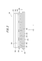
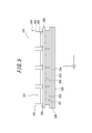
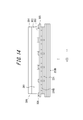
- FIG. 1 is a cross-sectional view schematically showing a configuration of a main part of an image display device according to a first embodiment. It is a figure which shows an example of the VCSEL arrangement
- light of sequential pixels of an image to be displayed is two-dimensionally deflected by a phased array according to the pixel position as parallel light flux from the observation surface, that is, light from infinity. Shoot out. This allows the observer to observe the image.
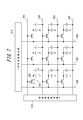
- FIG. 2 is a cross-sectional view schematically showing the configuration of the main part of the image display device according to the first embodiment.
- the image display apparatus 100 shown in FIG. 2 includes a light source unit 200 and a phase shift unit 300 that acts as an observation surface.
- the light source unit 200 includes, for example, a VCSEL array 202 including a plurality of surface emitting lasers (VCSELs) 201.
- the VCSEL array 202 can be of a known configuration disclosed in, for example, Japanese Patent Laid-Open No. 2005-45243, and has a common bottom mirror 203 and an active layer 204, and a top mirror 205 for each VCSEL.
- the VCSEL array 202 of this configuration can synchronize the phase of the laser light emitted from each of the VCSELs 201, and can emit coherent light.
- the configuration of the VCSEL array 202 is omitted for clarity of the drawing.
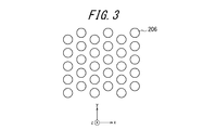
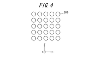
- the laser emission port 206 from which the laser light of each VCSEL 201 is emitted is set at a pitch of the wavelength level of the emitted laser light on the xy axis plane, for example, as shown in FIG. Arranged in the dimensional direction.
- FIGS. 3 and 4 are parts of a plan view of the VCSEL array 202 viewed from line II in FIG.
- the laser emission ports 206 are staggered at a half pitch of the array pitch in the x-axis direction and the y-axis direction.
- the laser emission ports 206 are squarely arranged in a lattice shape in the x-axis direction and the y-axis direction.
- the laser emission port 206 is shown circularly, it can be set as arbitrary shapes, such as a square and a hexagon.
- the z-axis direction indicates the emission direction of the laser light from each of the VCSELs 201 in the direction orthogonal to the x- and y-axis directions.
- the shapes and xyz axes of these laser emission ports are the same as in the other embodiments.
- the phase shift unit 300 is disposed optically coupled to the laser light emission side of the VCSEL array 202.
- the phase shift unit 300 includes a plurality of phase shift elements 301 corresponding to the VCSELs 201 of the VCSEL array 202.
- the phase shift element 301 is configured using, for example, a known electro-optical element such as KTN (potassium tantalate niobate) crystal, LN (lithium niobate) crystal, liquid crystal, or the like whose refractive index changes according to an applied voltage.
- KTN potassium tantalate niobate
- LN lithium niobate
- the phase shift element 301 has an area electrode portion 303 joined on the incident side of light from the VCSEL 201 and a transparent common electrode 304 commonly joined to the phase shift elements 301 on the light emission side. ing.
- the area electrode unit 303 includes, for example, a transparent area electrode and a TFT (Thin Film Transistor) which is a switching element connected to the area electrode.
- An X-axis wire 305 and a Y-axis wire 306 for selecting each phase shift element 301 are formed on the area electrode portion 303 side.
- the X-axis wiring 305 and the Y-axis wiring 306 are connected to an X-axis wiring drive circuit and a Y-axis wiring drive circuit described later, and the X-axis wiring 305 is driven by the X-axis wiring drive circuit.
- the axis wiring 306 is driven.
- the X-axis wiring drive circuit and the Y-axis wiring drive circuit can be configured to drive each phase shift element 301 by a passive matrix method, but are preferably configured to be driven by an active matrix method.
- the phase shift element 301 is configured by forming an area electrode portion 303 corresponding to each of the VCSELs 201 on one KTN crystal 302.
- the phase shift element 301 may be configured by forming the area electrode portion 303 on the KTN crystal 302 separated in units of the Y-axis wiring 306, for example.
- the phase shift element 301 may be configured by forming the area electrode portion 303 on the KTN crystal 302 separated in X-axis wiring units.
- the area electrode unit 303 can be configured with only the area electrode, for example, if the switching element can be formed outside the optical path of the phase shift element 301. In this case, the switching element does not necessarily have to be a TFT.
- n 0 is a refractive index
- ⁇ 0 is a vacuum dielectric constant
- ⁇ r is a relative dielectric constant
- d is a thickness of the KTN crystal 302 in the z-axis direction
- z is the z-axis direction from the region electrode 307 Indicates the distance of
- phase shift unit 300 drives the phase shift element 301 by the active matrix method
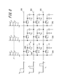
- FIG. 7 it is assumed that the VCSEL arrays 202 are arranged in a square as shown in FIG.
- the area electrode 307 and the TFT 308 are formed in the area electrode portion 303 of each phase shift element 301.
- the X-axis wiring 305 is connected to the X-axis wiring drive circuit 310
- the Y-axis wiring 306 is connected to the Y-axis wiring drive circuit 311.
- FIG. 7 shows an equivalent circuit of a drive circuit of the phase shift element 301. Since the KTN crystal 302 functions as a dielectric, it is represented as a capacitor "C”. The area electrode 307 is indicated by the symbol “E”, and the opposite common electrode 304 is indicated by the downward arrow.
- the region electrode E is connected to the drain D of the TFT 308, and the source S of the TFT 308 is connected to the corresponding Y-axis wiring 306, that is, the data line, and a required voltage is applied by the Y-axis wiring drive circuit 311.
- the gate G of the TFT 308 is connected to the corresponding X-axis wiring 305, that is, the scanning line.
- a storage capacitor Cs is formed between the area electrode E and the X axis wiring 305 of the next stage.
- symbols are mainly shown in parts corresponding to one phase shift element 301.
- FIG. 7 shows the array portion of the 3 ⁇ 3 phase shift element (area electrode E), but in reality the VCSEL array is composed of many VCSELs, and the area electrode E is also the same as the number of VCSELs. Existing.
- a voltage corresponding to the voltage data is applied from the Y-axis wiring drive circuit 311 to the corresponding area electrode E of the KTN crystal C via the Y-axis wiring 306, and corresponding from the X-axis wiring drive circuit 310 via the X-axis wiring 305.
- a control voltage for write scanning is applied to the gate G of the TFT 308.
- the write control voltage Vs is sequentially applied to the X axis wiring 305 from the upper side by the X axis wiring drive circuit 310 (scan).
- the control voltage Vs to the X-axis line 305 of the middle is applied.
- the control voltage Vs is applied to the gate G of the TFT 308, all the TFTs 308 connected to the X axis wiring 305 are turned on.
- charges are injected into the area electrode E connected to the drain D of the TFT 308, and the potential of each area electrode E becomes the same as the potential of the Y-axis wiring 306.
- a voltage to be applied to the KTN crystal C is applied to the area electrode E on each of the VCSELs.
- the voltage data at time t 0 are V 4 , V 5 and V 6 in order from the left Y-axis wiring 306, and the potential of the area electrode E along the central X-axis wiring 305 where the TFT 308 is on. Are respectively V 4 , V 5 and V 6 .
- the voltages applied to Y-axis wire 306 are V 1 , V 2 and V 3 , and the corresponding region
- the voltages applied to the electrode E are V 1 , V 2 and V 3 .
- the voltage applied to the area electrode E is held by the storage capacitor Cs.
- the X-axis wiring 305 is sequentially scanned from the top to the bottom, and data of the KTN applied voltage sent to the Y-axis wiring 306 is written to each area electrode E.
- each VCSEL 201 of the VCSEL array 202 is emitted as a plane wave of equal phase, but approaches the spherical wave by diffraction as the wave advances.
- the substantially spherical wave is incident on the phase shift unit 300.
- a desired voltage is applied to the area electrode E of each phase shift element of the phase shift unit 300, the light emitted from each phase shift element of the phase shift unit 300 becomes a substantially spherical wave having a phase change.
- the spherical waves having phase differences emitted from the respective phase shift elements of the phase shift unit 300 form the envelope surface E according to the principle of Huygens because the phase shift elements are arranged at the pitch of the wavelength level. That is, the light emitted from the VCSEL array 202 becomes one plane wave traveling in the direction of the arrow as a whole.
- phase difference ⁇ (for example, ⁇ 1 to ⁇ 7) is generated according to the above equation (3), the light flux from the VCSEL array 202 can be deflected.
- the deflection direction of the light flux can be changed continuously, and scanning of the light flux by a so-called phased array becomes possible.
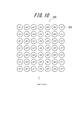
- FIG. 10 is a schematic view of the control of the phase difference by the phase shift unit 300 of FIG. 9 as viewed from the observation surface side.
- the phase difference sequentially increases or decreases in the phase shift elements 301 in each row in the x-axis direction, and the same phase difference is given to the phase shift elements 301 in each column in the y-axis direction, the x-axis
- the luminous flux can be deflected in the direction.
- the phase shift element 301 in each row in the y-axis direction sequentially increases or decreases, and if the phase shift element 301 in each row in the x-axis direction is given the same phase difference, light flux is generated in the y-axis direction. It can be deflected.
- deflection can be performed simultaneously in the x-axis direction and the y-axis direction.
- phased array it is possible to raster scan the light flux emitted from the VCSEL array 202.
- modulating the light intensity of the VCSEL array 202 according to the raster scan an image can be displayed.
- a light intensity modulator may be provided in the light path from the VCSEL array 202 to the viewer to display the image.
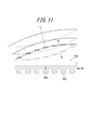
- the observer can observe the virtual image of the two-dimensional image by observing the phase shift unit 300.
- the observer can focus on a finite distance by emitting a spherical wave whose center of the sphere is on the far side of the device, that is, on the front side of the VCSEL array 202 from the observer. Even when combined, you can see the image clearly.
- a broken line in FIG. 11 by emitting a spherical wave in which the center of the sphere is on the rear side of the observer, it is possible for the observer with hyperopia to clearly observe the image. In this case, if a screen is installed, an image can be projected, and it can also be used as a projector.
- the pitch between VCSELs is 1.5 ⁇ m
- the size of the observation surface ie, the size of the aperture (pupil) is 100 mm ⁇ 50 mm
- the number of VCSELs is 66,667 It is 33 ⁇ 333 pieces. Therefore, in the case of driving by the active matrix method shown in FIG. 7, 33,333 X-axis wirings 305 are required, and 33,333 Vs signals may be sequentially output from the top to rewrite all the area electrodes once. It will be.
- the width of the Vs signal that is, the switching speed of the TFT 308 is 2 ps.
- the deflection control of the light flux is not limited to the case where it is performed by all the phase shift elements of the phase shift unit 300, but the phase shift unit 300 can be divided and controlled.
- the divided region in this case is preferably, for example, about 0.5 mm ⁇ 0.5 mm to several mm ⁇ several mm in which the spread due to diffraction does not adversely affect. In this case, it is not necessary to synchronize the phase of the VCSELs of different sections, and the light fluxes between the sections are mutually incoherent.
- the number of VCSELs is 333 ⁇ 333.
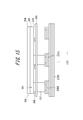
- FIG. 12 is a cross-sectional view schematically showing the configuration of the main part of the image display device according to the second embodiment.
- An image display apparatus 130 shown in FIG. 12 displays a color image, and the configuration of the light source unit is different from that of the image display apparatus 100 according to the first embodiment.
- the same components as those of the first embodiment are denoted by the same reference numerals, and the description thereof is omitted.
- the light source unit 230 includes, for example, a VCSEL array 232R having a plurality of VCSELs 231R emitting a red laser beam (R), a VCSEL array 232G having a plurality of VCSELs 231G emitting a green laser beam (G), and a blue color And a VCSEL array 232B having a plurality of VCSELs 231B for emitting laser light (B).
- the VCSEL arrays 232R, 232G and 232B respectively have a common bottom mirror 233, an active layer 234 corresponding to the wavelength of the emitted laser light, and a top mirror for each VCSEL.
- H.235 Similar to the VCSEL array 202 described in the first embodiment, the VCSEL arrays 232R, 232G and 232B respectively have a common bottom mirror 233, an active layer 234 corresponding to the wavelength of the emitted laser light, and a top mirror for each VCSEL. And H.235.
- each of the VCSEL arrays 232R, 232G and 232B is omitted.
- illustration of the X axis wiring and the Y axis wiring of the phase shift unit 300 is omitted.
- FIG. 13 is a part of a plan view of the VCSEL arrays 232R, 232G and 232B viewed from line II-II in FIG. That is, for the rows in the x-axis direction, a repeated pattern of R rows, B rows, B rows, and G rows is taken, and for the columns in the y-axis direction, B and G alternate and R and B alternate. It makes it a repeating pattern with the lined line.
- the pitch of the laser emitting ports of the same color and the pitch of the adjacent laser emitting ports are 2 ⁇ m in the x-axis direction and 2.3 ⁇ m in the y-axis direction for the laser emitting ports of the same color.
- the pitch in the x-axis direction can be 1 ⁇ m
- the pitch in the y-axis direction can be 1.15 ⁇ m.
- the VCSEL array 232B is optically coupled to the phase shift unit 300 having the same configuration as that of the first embodiment as the laser emission port 236B side is schematically shown in FIG. 14 along the line III-III in FIG. Be done.
- the VCSEL array 232G is optically coupled to the phase shift unit 300 via the waveguide 237, as schematically shown by the IV-IV line cross section in FIG. 13 in FIG.
- the VCSEL array 232R is optically coupled to the phase shift unit 300 via the waveguide 238, as schematically shown by the VV cross section in FIG.
- the phase shift unit 300 has a plurality of phase shift elements 301 corresponding to the VCSELs 231R, 231G and 231B of the VCSEL arrays 232R, 232G and 232B.
- the number of VCSELs 231 B emitting blue laser light is increased, and the pitch of the adjacent VCSELs 231 B is decreased.
- the reason is that, from the above equation (3), since the emission angle ⁇ is small when the wavelength ⁇ is short, the number is increased and the pitch is reduced for the VCSEL 231B that emits blue laser light having a short wavelength ⁇ , This is to make it possible to obtain a desired emission angle ⁇ .
- the pitches in the x-axis direction and the y-axis direction can be made different according to the angle of view in each of the x-axis and y-axis directions.
- the VCSEL arrays 232R, 232G and 232B of the respective colors are lighted sequentially or simultaneously according to the color information of the pixel to be displayed.
- the phase shift unit 300 scans the emitted light in a two-dimensional direction by the phased array according to the pixel position to be displayed.
- the observer can observe a color image by observing the phase shift unit 300.
- Wavelength R: 640 nm, G: 530 nm, B: 450 nm
- phase shift elements pitch between VCSELs: as shown in FIG. 13 thickness of KTN crystal d: 1 ⁇ m
- Applied voltage to KTN crystal 0 to 4.18 V (phase difference 0 to ⁇ )
- Observation plane size 200 mm ⁇ 100 mm
- Frame rate: 30 fps X axis wiring number number of scanning lines: 600 to 1080
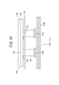
- FIG. 17 is a cross-sectional view schematically showing the configuration of the main part of the image display device according to the third embodiment.
- An image display device 160 shown in FIG. 17 displays a color image, and the configuration of the light source unit is different from that of the image display device 100 of the first embodiment.
- the same components as those of the first embodiment are denoted by the same reference numerals, and the description thereof is omitted.
- the light source unit 260 emits, for example, a laser diode 261R that emits red laser light (R), a laser diode 261G that emits green laser light (G), and blue laser light (B).
- a laser diode 261 B, three collimator lenses 262, 263 and 264, two dichroic mirrors 265 and 266, and a beam expander 267 are provided.
- the red laser light emitted from the laser diode 261R is converted into parallel light by the collimator lens 262 and sequentially transmitted through the dichroic mirrors 265 and 263. Then, the light expander is expanded by the beam expander 267 and the phase shift unit 300 is converted into parallel light.
- the green laser light emitted from the laser diode 261 G is converted into parallel light by the collimator lens 263, reflected by the dichroic mirror 265, and coaxially synthesized with the optical path of the red laser light, and then transmitted through the dichroic mirror 266.
- the light beam is expanded by the beam expander 267 and is incident on the phase shift unit 300 as parallel light.
- the blue laser light emitted from the laser diode 261 B is converted into parallel light by the collimator lens 264, reflected by the dichroic mirror 266, and coaxially synthesized with the optical paths of the red laser and the green laser light.
- the light flux is expanded and is incident on the phase shift unit 300 as parallel light.
- the laser diodes 261 R, 261 G and 261 B of each color are sequentially or simultaneously turned on according to the color information of the pixel to be displayed.
- the phase shift unit 300 is configured to include a plurality of phase shift elements 301 arranged in a two-dimensional direction at the pitch of the wavelength level, and in the same manner as the first embodiment, the emitted light according to the pixel position to be displayed In a two-dimensional direction by a phased array.
- the observer can observe a color image by observing the phase shift unit 300.
- the present invention is not limited to the above embodiment, and various modifications or changes can be made without departing from the scope of the invention.
- the light source is not limited to three colors of RGB, and may be configured to emit light of wavelengths of four or more colors including yellow, for example.
- the refractive index change by an electro-optic crystal was used for the phase shift in the said embodiment, the refractive index change by the carrier plasma effect can also be used.
Landscapes
- Physics & Mathematics (AREA)
- Optics & Photonics (AREA)
- Nonlinear Science (AREA)
- General Physics & Mathematics (AREA)
- Engineering & Computer Science (AREA)
- Multimedia (AREA)
- Signal Processing (AREA)
- Condensed Matter Physics & Semiconductors (AREA)
- Electromagnetism (AREA)
- Liquid Crystal (AREA)
- Optical Modulation, Optical Deflection, Nonlinear Optics, Optical Demodulation, Optical Logic Elements (AREA)
- Devices For Indicating Variable Information By Combining Individual Elements (AREA)
Priority Applications (1)
| Application Number | Priority Date | Filing Date | Title |
|---|---|---|---|
| US15/014,431 US9843778B2 (en) | 2013-08-05 | 2016-02-03 | Image display device |
Applications Claiming Priority (2)
| Application Number | Priority Date | Filing Date | Title |
|---|---|---|---|
| JP2013162682A JP6143601B2 (ja) | 2013-08-05 | 2013-08-05 | 画像表示装置 |
| JP2013-162682 | 2013-08-05 |
Related Child Applications (1)
| Application Number | Title | Priority Date | Filing Date |
|---|---|---|---|
| US15/014,431 Continuation US9843778B2 (en) | 2013-08-05 | 2016-02-03 | Image display device |
Publications (1)
| Publication Number | Publication Date |
|---|---|
| WO2015019551A1 true WO2015019551A1 (ja) | 2015-02-12 |
Family
ID=52460913
Family Applications (1)
| Application Number | Title | Priority Date | Filing Date |
|---|---|---|---|
| PCT/JP2014/003681 Ceased WO2015019551A1 (ja) | 2013-08-05 | 2014-07-10 | 画像表示装置 |
Country Status (3)
| Country | Link |
|---|---|
| US (1) | US9843778B2 (enExample) |
| JP (1) | JP6143601B2 (enExample) |
| WO (1) | WO2015019551A1 (enExample) |
Cited By (2)
| Publication number | Priority date | Publication date | Assignee | Title |
|---|---|---|---|---|
| EP3179306A1 (en) * | 2015-12-11 | 2017-06-14 | Samsung Electronics Co., Ltd. | Beam steering apparatus, method of driving the beam steering apparatus, and spatial information acquisition apparatus using the beam steering apparatus |
| JP2023077078A (ja) * | 2021-11-24 | 2023-06-05 | 日産自動車株式会社 | 半導体装置及び物体検出装置 |
Families Citing this family (2)
| Publication number | Priority date | Publication date | Assignee | Title |
|---|---|---|---|---|
| JP7150648B2 (ja) | 2019-03-20 | 2022-10-11 | 三菱重工業株式会社 | 超音波探傷装置及び超音波探傷方法並びに超音波探傷プログラム |
| WO2021140752A1 (ja) * | 2020-01-10 | 2021-07-15 | ソニーグループ株式会社 | 映像投影装置 |
Citations (7)
| Publication number | Priority date | Publication date | Assignee | Title |
|---|---|---|---|---|
| JPH06138499A (ja) * | 1992-03-25 | 1994-05-20 | Motorola Inc | 直接網膜スキャン・ディスプレイ |
| JPH06504633A (ja) * | 1991-10-09 | 1994-05-26 | ヒューズ・エアクラフト・カンパニー | 光学フェイズドアレイ |
| JPH08163602A (ja) * | 1994-12-06 | 1996-06-21 | Nippon Telegr & Teleph Corp <Ntt> | 立体表示装置 |
| JPH1152404A (ja) * | 1997-06-12 | 1999-02-26 | Sharp Corp | 回折型空間光変調器およびディスプレイ |
| JP2004511017A (ja) * | 2000-09-29 | 2004-04-08 | ロックウェル・サイエンティフィック・ライセンシング・エルエルシー | 周波数変調式液晶ビーム・ステアリング装置 |
| JP2007011104A (ja) * | 2005-07-01 | 2007-01-18 | National Institute Of Information & Communication Technology | 光線制御装置及びそれを用いた立体像表示装置 |
| JP2012173341A (ja) * | 2011-02-17 | 2012-09-10 | Nippon Telegr & Teleph Corp <Ntt> | 空間光位相変調器 |
Family Cites Families (5)
| Publication number | Priority date | Publication date | Assignee | Title |
|---|---|---|---|---|
| WO1994019765A1 (en) | 1993-02-19 | 1994-09-01 | Norand Corporation | Phased array laser scanner |
| CN1096004C (zh) * | 1997-11-05 | 2002-12-11 | 朱润枢 | 相控阵光学装置 |
| US7397980B2 (en) | 2004-06-14 | 2008-07-08 | Optium Australia Pty Limited | Dual-source optical wavelength processor |
| JP5084540B2 (ja) * | 2008-02-06 | 2012-11-28 | キヤノン株式会社 | 垂直共振器型面発光レーザ |
| US8515217B2 (en) * | 2009-09-02 | 2013-08-20 | Alcatel Lucent | Vertical optically emitting photonic devices with electronic steering capability |
-
2013
- 2013-08-05 JP JP2013162682A patent/JP6143601B2/ja active Active
-
2014
- 2014-07-10 WO PCT/JP2014/003681 patent/WO2015019551A1/ja not_active Ceased
-
2016
- 2016-02-03 US US15/014,431 patent/US9843778B2/en active Active
Patent Citations (7)
| Publication number | Priority date | Publication date | Assignee | Title |
|---|---|---|---|---|
| JPH06504633A (ja) * | 1991-10-09 | 1994-05-26 | ヒューズ・エアクラフト・カンパニー | 光学フェイズドアレイ |
| JPH06138499A (ja) * | 1992-03-25 | 1994-05-20 | Motorola Inc | 直接網膜スキャン・ディスプレイ |
| JPH08163602A (ja) * | 1994-12-06 | 1996-06-21 | Nippon Telegr & Teleph Corp <Ntt> | 立体表示装置 |
| JPH1152404A (ja) * | 1997-06-12 | 1999-02-26 | Sharp Corp | 回折型空間光変調器およびディスプレイ |
| JP2004511017A (ja) * | 2000-09-29 | 2004-04-08 | ロックウェル・サイエンティフィック・ライセンシング・エルエルシー | 周波数変調式液晶ビーム・ステアリング装置 |
| JP2007011104A (ja) * | 2005-07-01 | 2007-01-18 | National Institute Of Information & Communication Technology | 光線制御装置及びそれを用いた立体像表示装置 |
| JP2012173341A (ja) * | 2011-02-17 | 2012-09-10 | Nippon Telegr & Teleph Corp <Ntt> | 空間光位相変調器 |
Cited By (3)
| Publication number | Priority date | Publication date | Assignee | Title |
|---|---|---|---|---|
| EP3179306A1 (en) * | 2015-12-11 | 2017-06-14 | Samsung Electronics Co., Ltd. | Beam steering apparatus, method of driving the beam steering apparatus, and spatial information acquisition apparatus using the beam steering apparatus |
| US10503045B2 (en) | 2015-12-11 | 2019-12-10 | Samsung Electronics Co., Ltd. | Beam steering apparatus, method of driving the beam steering apparatus, and spatial information acquisition apparatus using the beam steering apparatus |
| JP2023077078A (ja) * | 2021-11-24 | 2023-06-05 | 日産自動車株式会社 | 半導体装置及び物体検出装置 |
Also Published As
| Publication number | Publication date |
|---|---|
| US20160156885A1 (en) | 2016-06-02 |
| US9843778B2 (en) | 2017-12-12 |
| JP6143601B2 (ja) | 2017-06-07 |
| JP2015031881A (ja) | 2015-02-16 |
Similar Documents
| Publication | Publication Date | Title |
|---|---|---|
| US11144010B2 (en) | Focus modulation optical system and holographic display device having the same | |
| US10490140B2 (en) | Light deflector and display apparatus | |
| US10951867B2 (en) | Light emitter architecture for scanning display device | |
| TWI872142B (zh) | 具有提高的均勻性和/或眼睛安全性的雷射照射顯示器 | |
| US20080117491A1 (en) | Illumination systems for visual displays | |
| JP6107185B2 (ja) | 画像形成装置、及び画像表示装置 | |
| KR102098549B1 (ko) | 다중 뷰 디스플레이에 대한 지향성 픽셀 | |
| JP4930071B2 (ja) | 表示装置 | |
| JP4229192B2 (ja) | 電気光学素子及び走査型光学装置 | |
| KR20110009631A (ko) | 전기 광학 장치의 구동 장치, 전기 광학 장치 및 전자 기기 | |
| JP6143601B2 (ja) | 画像表示装置 | |
| JP6549909B2 (ja) | 光線制御素子および立体表示装置 | |
| US20240223744A1 (en) | Multiple-views-one-eye display method with sub-pixels as basic display units | |
| EP3712681A1 (en) | Display device | |
| JP6305855B2 (ja) | 画像表示装置 | |
| CN118363174A (zh) | 头部佩戴型显示装置和光学单元 | |
| JP6737319B2 (ja) | プロジェクターおよびプロジェクターの制御方法 | |
| US20210271086A1 (en) | Waveguide-based display module, and image generation module and application thereof | |
| US8773613B2 (en) | Liquid-crystal display with coherent illumination and reduced speckling | |
| KR20190125852A (ko) | 빔 편향기, 이를 포함한 홀로그래픽 디스플레이 장치 및 빔 편향기 구동 방법 | |
| JP2013044836A (ja) | 映像表示装置 | |
| KR102595759B1 (ko) | 광 변조기 및 이를 포함하는 홀로그래픽 표시 장치 | |
| US20230061336A1 (en) | Optical-waveguide display module with multiple light sources | |
| CN118169884A (zh) | 虚像显示装置以及头部佩戴型显示装置 | |
| JP2024082375A (ja) | 虚像表示装置及び頭部装着型表示装置 |
Legal Events
| Date | Code | Title | Description |
|---|---|---|---|
| 121 | Ep: the epo has been informed by wipo that ep was designated in this application |
Ref document number: 14835155 Country of ref document: EP Kind code of ref document: A1 |
|
| NENP | Non-entry into the national phase |
Ref country code: DE |
|
| 122 | Ep: pct application non-entry in european phase |
Ref document number: 14835155 Country of ref document: EP Kind code of ref document: A1 |