WO2015019524A1 - ダイバーシティ受信回路 - Google Patents
ダイバーシティ受信回路 Download PDFInfo
- Publication number
- WO2015019524A1 WO2015019524A1 PCT/JP2014/002142 JP2014002142W WO2015019524A1 WO 2015019524 A1 WO2015019524 A1 WO 2015019524A1 JP 2014002142 W JP2014002142 W JP 2014002142W WO 2015019524 A1 WO2015019524 A1 WO 2015019524A1
- Authority
- WO
- WIPO (PCT)
- Prior art keywords
- receiving circuit
- diversity receiving
- circuit
- switch
- diversity
- Prior art date
- Legal status (The legal status is an assumption and is not a legal conclusion. Google has not performed a legal analysis and makes no representation as to the accuracy of the status listed.)
- Ceased
Links
Images









Classifications
-
- H—ELECTRICITY
- H04—ELECTRIC COMMUNICATION TECHNIQUE
- H04B—TRANSMISSION
- H04B7/00—Radio transmission systems, i.e. using radiation field
- H04B7/02—Diversity systems; Multi-antenna system, i.e. transmission or reception using multiple antennas
- H04B7/04—Diversity systems; Multi-antenna system, i.e. transmission or reception using multiple antennas using two or more spaced independent antennas
- H04B7/08—Diversity systems; Multi-antenna system, i.e. transmission or reception using multiple antennas using two or more spaced independent antennas at the receiving station
- H04B7/0802—Diversity systems; Multi-antenna system, i.e. transmission or reception using multiple antennas using two or more spaced independent antennas at the receiving station using antenna selection
Definitions
- the present invention relates to a diversity receiving circuit.
- each PLL in the diversity receiving circuit is provided with an independent PLL (phase-locked loop) as a local oscillation unit, four PLLs are arranged in one chip. Will accumulate on top. In this case, since each PLL occupies a relatively large area, the chip area becomes large. In addition, as a result of interference between a plurality of PLLs whose oscillation frequencies approximate to each other, spurious and noise increase, and the risk of degradation of reception sensitivity increases.
- PLL phase-locked loop
- the frequency of the branch sharing the PLL is fixed to be the same, so the degree of freedom is low.
- An object of the present invention is to provide a diversity receiving circuit having a small area that can reduce spurious and noise and improve performance such as reception sensitivity.
- the present invention provides a diversity receiving circuit that obtains a composite output based on signals respectively received by a plurality of antennas, a plurality of local oscillating units that each output a local oscillation signal, and a high-frequency receiving unit.
- a plurality of frequency converters for converting a signal into a low-frequency signal, and at least one of the plurality of frequency converters, the output of the plurality of local oscillators is selected before the frequency converter
- a switch circuit to be supplied to the conversion unit is selected before the frequency converter.
- the diversity receiving circuit according to the present invention can reduce the circuit area, reduce spurious and noise due to interference, and improve performance such as reception sensitivity, as compared with a configuration including an independent local oscillation unit in each branch. Further, since the local oscillator can be selected flexibly by switching the switch circuit, a high degree of freedom can be obtained.
- FIG. 2 is a circuit diagram illustrating a detailed configuration example of a switch circuit in FIG. 1.
- FIG. 3 is a circuit diagram illustrating another detailed configuration example of the switch circuit in FIG. 1.
- FIG. 6 is a circuit diagram showing still another detailed configuration example of the switch circuit in FIG. 1. It is a circuit diagram which shows the example of the power supply wiring in the diversity receiver circuit of FIG. 1, and a ground wiring.
- FIG. 6 is a circuit diagram illustrating another example of a power supply wiring and a ground wiring in the diversity receiving circuit of FIG. 1.
- FIG. 6 is a circuit diagram showing still another example of power supply wiring and ground wiring in the diversity receiving circuit of FIG. 1. It is a figure which shows the other example of the state transition in the diversity receiver circuit of FIG. It is a figure which shows the further another example of the state transition in the diversity receiver circuit of FIG. It is a block diagram which shows the modification of the diversity receiver circuit of FIG.
- FIG. 12 is a circuit diagram illustrating an example of a power supply wiring and a ground wiring in the diversity receiving circuit of FIG. 11.
- FIG. 12 is a circuit diagram illustrating another example of a power supply wiring and a ground wiring in the diversity receiving circuit of FIG. 11. It is a block diagram which shows the structure of the diversity receiver circuit which concerns on the 2nd Embodiment of this invention. It is a figure which shows an example of the state transition in the diversity receiver circuit of FIG.
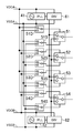
- FIG. 1 is a block diagram showing a configuration of a diversity receiving circuit according to the first embodiment of the present invention.
- the diversity receiving circuit of FIG. 1 is configured as a monolithic semiconductor circuit 100 for a TV tuner so as to obtain combined outputs TS1 and TS2 based on signals received by four antennas 11 to 14, respectively.
- the high frequency reception signals input from the antennas 11 to 14 are matched by the matching circuits 21 to 24 and input to the monolithic semiconductor circuit 100.
- the matched high frequency signal is first amplified by low noise amplifiers (LNA) 31-34.
- LNA low noise amplifiers
- the local oscillation signals generated by the first and second PLLs 41 and 42 are selected by the switch circuits (SW) 51 to 54 and are divided by the frequency dividing circuits (DIV) 61 to 64, respectively.
- the outputs of the LNAs 31 to 34 are converted into low frequency signals by the mixers (MIX) 71 to 74 by the outputs of the frequency dividing circuits 61 to 64, the band is limited by the filters (FIL) 81 to 84, and the ADC (analog ⁇ to-digital converter) 91-94, converted into digital signals, demodulated by demodulation circuits (DEMOD) 101-104, synthesized by diver synthesis circuit 201, and output as transport stream signals TS1, TS2. .
- the control circuit 301 controls each block of the monolithic semiconductor circuit 100 based on the control input.
- the first and second PLLs 41 and 42 and the switch circuits 51 to 54 related to the present invention are particularly shown. Only control is shown. Further, a portion constituted by the antenna 11, the matching circuit 21, the LNA 31, the switch circuit 51, the frequency divider circuit 61, the mixer 71, the filter 81, the ADC 91, and the demodulation circuit 101 is referred to as a branch 1, and so on. To do.
- the power and ground of the first PLL 41 and the power and ground of the second PLL 42 are separated from each other.
- 111 is a power pad of the first PLL 41
- 112 is a power pad of the second PLL 42
- 113 is a ground pad of the first PLL 41
- 114 is a ground pad of the second PLL 42.
- any one of the first and second PLLs 41 and 42 is supplied to the mixers 71 to 74 via the frequency divider circuits 61 to 64. Can communicate.
- 0 And converted to near DC.
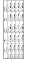
- FIG. 2 is a diagram illustrating an example of state transition in the diversity receiving circuit of FIG.
- the diversity receiving circuit of FIG. 1 can arbitrarily select the first and second PLLs 41 and 42 in the switch circuits 51 to 54. Therefore, for example, when the sensitivity of the branch 3 is poorer than that of the other branches, the branches 1, 2, and 4 are selected by the first PLL 41 and output as TS1, and the branch 3 is set to the second while keeping the main screen. It is possible to use such as selecting a channel by the PLL 42, outputting it by TS2, and using it for searching for another station (state (2)).
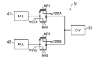
- FIG. 3 is a circuit diagram showing a detailed configuration example of the switch circuit 51 in FIG.
- the other switch circuits 52 to 54 are the same as in FIG. 3 includes a one-stage transfer gate inserted between the output of the first PLL 41 and the input of the frequency dividing circuit 61, and the output of the second PLL 42 and the input of the frequency dividing circuit 61. It consists of a one-stage transfer gate inserted between them.
- the former transfer gate includes a PMOS transistor MP1 whose back gate is connected to the power supply VDDA and an NMOS transistor MN1 whose back gate is connected to the ground VSSA.
- the latter transfer gate includes a PMOS transistor MP2 whose back gate is connected to the power supply VDDB and an NMOS transistor MN2 whose back gate is connected to the ground VSSB.
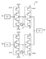
- FIG. 4 is a circuit diagram showing another detailed configuration example of the switch circuit 51 in FIG.
- the other switch circuits 52 to 54 are the same as in FIG. 4 includes a two-stage transfer gate inserted in the first path between the output of the first PLL 41 and the input of the frequency divider circuit 61, the output of the second PLL 42, and the frequency divider circuit 61. And a two-stage transfer gate inserted in the second path to the input.
- the first-stage transfer gate includes a PMOS transistor MP1 whose back gate is connected to the power supply VDDA and an NMOS transistor MN1 whose back gate is connected to the ground VSSA.
- the first-stage transfer gate includes a PMOS transistor MP2 whose back gate is connected to the power supply VDDB and an NMOS transistor MN2 whose back gate is connected to the ground VSSB.
- the connection node between the first-stage transfer gate and the second-stage transfer gate is connected to the ground VSSA through the NMOS transistor MN5. Further, the connection node between the first-stage transfer gate and the second-stage transfer gate is connected to the ground VSSB via the NMOS transistor MN6 in the second path.
- the switch circuit 51 selects the output of the first PLL 41, MP1, MN1, MP3 and MN3 are turned on, MN5 is turned off, and the first PLL 41 is turned on.
- the output is transmitted to the frequency dividing circuit 61.
- MP2, MN2, MP4, and MN4 are off, but by turning on MN6, the connection node of the two-stage transfer gate on the second PLL 42 side that is not selected can be grounded. That is, the switch circuit 51 of FIG. 4 is configured to ensure isolation performance between the non-selected input and the output, and thereby interference between the output of the first PLL 41 and the output of the second PLL 42. Can be reduced. Note that three or more transfer gates may be used.
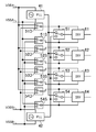
- FIG. 5 is a circuit diagram showing still another detailed configuration example of the switch circuit 51 in FIG.
- the other switch circuits 52 to 54 are the same as in FIG.
- the switch circuit 51 of FIG. 5 includes two-stage tris state inverters INV1 and INV3 inserted in the first path between the output of the first PLL 41 and the input of the frequency divider circuit 61, and the output of the second PLL 42. It is composed of two-stage tris state inverters INV2 and INV4 inserted in the second path between the frequency divider 61 and the input.
- the two-stage trisstate inverters INV1 and INV3 on the first path are connected to the power supply VDDA and the ground VSSA, and the two-stage trisstate inverters INV2 and INV4 on the second path are connected to the power supply VDDB and the ground VSSB, respectively.
- the connection node between the first-stage trisstate inverter INV1 and the second-stage trisstate inverter INV3 is connected to the ground VSSA via the NMOS transistor MN5.
- a connection node between the first-stage trisstate inverter INV2 and the second-stage trisstate inverter INV4 is connected to the ground VSSB via the NMOS transistor MN6 in the second path.
- the switch circuit 51 selects the output of the first PLL 41, INV1 and INV3 are turned on, MN5 is turned off, and the output of the first PLL 41 is divided. The signal is transmitted to the circuit 61 without being attenuated.
- INV2 and INV4 are off, by turning on MN6, the connection node of the two-stage tris-state inverters INV2 and INV4 on the second PLL 42 side that are not selected can be grounded. That is, the switch circuit 51 of FIG. 5 is configured to ensure isolation performance between the non-selected input and the output, and thereby interference between the output of the first PLL 41 and the output of the second PLL 42. Can be reduced.
- a tri-state inverter having three or more stages may be used.
- FIG. 6 is a circuit diagram showing an example of power supply wiring and ground wiring in the diversity receiving circuit of FIG.
- the power supply VDDA and ground VSSA of the first PLL 41 and the power supply VDDB and ground VSSB of the second PLL 42 are: Are separated from each other.
- the switch circuits 51 to 52 and the frequency dividing circuits 61 to 62 are fixedly connected to VDDA and VSSA, and the switch circuits 53 to 54 and the frequency dividing circuits 63 to 64 are fixedly connected to VDDB and VSSB.
- FIG. 7 is a circuit diagram showing another example of the power supply wiring and the ground wiring in the diversity receiving circuit of FIG. According to FIG. 7, the power supply VDDA and ground VSSA of the first PLL 41 and the power supply VDDB and ground VSSB of the second PLL 42 are separated from each other.
- VDD switches 51D to 54D and VSS switches 51S to 54S are provided for the switch circuits 51 to 54 and the frequency dividing circuits 61 to 64, respectively.
- the VDD switches 51D to 54D and the VSS switches 51S to 54S supply the power supply voltage or the ground voltage supplied to the PLL selected by the corresponding switch circuit to the corresponding switch circuit and the frequency dividing circuit. Control is performed in conjunction with the switch circuits 51-54.
- the VDD switch 51D when the switch circuit 51 selects the output of the first PLL 41, the VDD switch 51D connects the VDDA of the first PLL 41 to the switch circuit 51 and the frequency dividing circuit 61, and the VSS switch 51S is the first PLL 41. Are connected to the switch circuit 51 and the frequency dividing circuit 61. Conversely, when the switch circuit 51 selects the output of the second PLL 42, the VDD switch 51D connects the VDDB of the second PLL 42 to the switch circuit 51 and the frequency divider 61, and the VSS switch 51S The VSSB of the PLL 42 is connected to the switch circuit 51 and the frequency dividing circuit 61.
- FIG. 8 is a circuit diagram showing still another example of the power supply wiring and the ground wiring in the diversity receiving circuit of FIG.
- the power supply VDDA and ground VSSA of the first PLL 41 and the power supply VDDB and ground VSSB of the second PLL 42 are separated from each other.
- the switch circuit 51 and the frequency divider 61 in the branch 1 are connected to the power supply VDDC and the ground VSSC
- the switch circuit 52 and the frequency divider 62 in the branch 2 are connected to the power supply VDDD and the ground VSSD
- the switch circuit 53 and the frequency divider in the branch 3 are connected.
- the switch circuit 54 and the frequency dividing circuit 64 of the branch 4 are connected to the power supply VDDF and the ground VSSF, respectively.
- the VDDA and VSSSA of the first PLL 41 and the VDDB and VSSB of the second PLL 42 are connected. Independent from. As described above, by using independent power supply wiring and ground wiring for the switch circuits 51 to 54 and the frequency dividing circuits 61 to 64, interference between the first PLL 41 and the second PLL 42 can be prevented.
- a dedicated PLL is not required for each branch, and two PLLs 41 and 42 are provided.
- a function capable of selecting an arbitrary channel In general, a PLL used for a diversity receiving circuit has an LC tank type VCO (voltage-controlled oscillator) with low phase noise and requires an area. Therefore, by making the number of PLLs smaller than the number of branches, it is possible to contribute to the reduction of the area of the monolithic semiconductor circuit 100, that is, the cost reduction. Further, as the number of PLLs increases, the risk of mutual interference among the PLLs increases accordingly, but by reducing the number of PLLs to two, it is only necessary to pay attention to the interference between the two PLLs 41 and 42.
- the power supply pad 111 and the ground pad 113 of the first PLL 41 and the power supply pad 112 and the ground pad 114 of the second PLL 42 are separated from each other. Interference with the second PLL 42 can be reduced. Further, as shown in FIG. 1, by arranging the pads 111 to 114 in the vicinity of different sides of the monolithic semiconductor circuit 100, the influence of the coupling of the wiring inductor and the influence of the semiconductor substrate can be reduced. it can.
- FIG. 9 is a diagram showing another example of state transition in the diversity receiving circuit of FIG.
- the state (3) in FIG. 9 when one PLL system becomes the same channel during the search operation or when the same channel is selected on both screens, as shown in the state (3) of FIG.
- the selected PLL is selected by all the switch circuits 51 to 54 including the branch being searched and the control circuit 301 is configured to stop the operation of the unused PLL, the same frequency is received. It is possible to reduce the influence of interference at the time. Further, since interference is likely to occur when the operating frequencies of the respective PLLs are close to each other, the frequency may be set to be different from that of the PLL using the unused PLL. It is also possible to change the number of branches used for the search to 2 or more.
- FIG. 10 is a diagram showing still another example of state transition in the diversity receiving circuit of FIG.
- the channel of the second PLL 42 at the end of the search is used as it is.
- the most appropriate channel is selected again by the first PLL 41 after the end of the search. May be.
- the first PLL 41 uses a high-performance PLL
- the second PLL 42 uses a PLL having different performance such as low power consumption.
- the high-performance first PLL 41 is used for a main screen or a branch for normal reception. If the second PLL 42 with low power consumption is selected for the sub-screen or the branch for receiving search among the two screens, it is possible to achieve both high performance and low power consumption.
- FIG. 11 is a block diagram showing a modification of the diversity receiving circuit of FIG.
- a first frequency divider 61 is provided between the first PLL 41 and the switch circuits 51 to 54
- a second frequency divider 62 is provided between the second PLL 42 and the switch circuits 51 to 54, respectively. Has been inserted.
- FIG. 12 is a circuit diagram showing an example of power supply wiring and ground wiring in the diversity receiving circuit of FIG.
- the power supply VDDA and ground VSSA of the first PLL 41 and the first frequency divider circuit 61 and the power supply VDDB and ground VSSB of the second PLL 42 and the second frequency divider circuit 62 are separated from each other.
- VDD switches 51D to 54D and VSS switches 51S to 54S are provided for the switch circuits 51 to 54, respectively.
- the VDD switches 51D to 54D and the VSS switches 51S to 54S are configured to supply the power supply voltage or the ground voltage supplied to the PLL and the frequency dividing circuit selected by the corresponding switch circuit to the corresponding switch circuit.
- Control is performed in conjunction with the switch circuits 51-54.
- the switch circuit 51 selects the output of the first PLL 41
- the VDD switch 51D connects the VDDA of the first PLL 41 and the first frequency dividing circuit 61 to the switch circuit 51, and the VSS switch 51S 1 PLL 41 and VSSA of the first frequency divider 61 are connected to the switch circuit 51.
- the switch circuit 51 selects the output of the second PLL 42
- the VDD switch 51D connects the VDDB of the second PLL 42 and the second frequency divider 62 to the switch circuit 51, and the VSS switch 51S VSSB of the second PLL 42 and the second frequency divider 62 is connected to the switch circuit 51.
- FIG. 13 is a circuit diagram showing another example of the power supply wiring and the ground wiring in the diversity receiving circuit of FIG.
- the power supply VDDA and ground VSSA of the first PLL 41 and the first frequency divider circuit 61 and the power supply VDDB and ground VSSB of the second PLL 42 and the second frequency divider circuit 62 are separated from each other.
- the switch circuit 51 of the branch 1 is connected to the power supply VDDC and the ground VSSC
- the switch circuit 52 of the branch 2 is connected to the power supply VDDD and the ground VSSD
- the switch circuit 53 of the branch 3 is connected to the power supply VDDE and the ground VSSE
- the switch circuit 54 of the branch 4 is connected.
- FIG. 14 is a block diagram showing a configuration of a diversity receiving circuit according to the second embodiment of the present invention.
- two PLLs 41 and 42 are provided in a 2-branch diversity receiving circuit.
- a switch circuit 51 for selecting one of the outputs of the first and second PLLs 41 and 42 is provided in front of the frequency divider 61 and the mixer 71 in the branch 1, and in front of the frequency divider 62 and the mixer 72 in the branch 2.
- a switch circuit 52 for selecting one of the outputs of the first and second PLLs 41 and 42 is provided.
- FIG. 15 is a diagram illustrating an example of state transition in the diversity reception circuit of FIG. Since the outputs of the first and second PLLs 41 and 42 can be arbitrarily selected in each of the switch circuits 51 and 52, normal reception in one screen such as the state (1) and the state (5), and the state (3) Thus, when the same channel is selected during search or when two screens are used, interference can be prevented by operating with one PLL. In addition, smooth reception can be realized by using the PLL that has been searched as it is for normal reception as in the transition from state (4) to state (5).
- the first and second embodiments have been described as examples of the technology disclosed in the present application.
- the technology in the present application is not limited to this, and can also be applied to embodiments in which changes, replacements, additions, omissions, etc. have been made as appropriate.
- the switch circuits 51 to 54 are placed in front of all the mixers 71 to 74, but only a part may be used. Even in such a case, the mixer provided with the switch circuit can be switched, which is effective. 6 to 8 show examples in which both the power supply wiring and the ground wiring are separated, but one side may be used.
- the diversity receiving circuit according to the present invention is useful as a technique that can reduce spurious and noise due to interference when receiving signals of a plurality of frequencies, improve performance such as reception sensitivity, and reduce the mounting area and chip area. .
Landscapes
- Engineering & Computer Science (AREA)
- Computer Networks & Wireless Communication (AREA)
- Signal Processing (AREA)
- Radio Transmission System (AREA)
- Circuits Of Receivers In General (AREA)
Abstract
複数のアンテナ(11~14)でそれぞれ受信した信号をもとに合成出力(TS1,TS2)を得るダイバーシティ受信回路において、各々局部発振信号を出力する複数のPLL(41,42)と、各々高周波受信信号を低周波信号に変換する複数のミキサ(71~74)と、各ミキサ(71~74)の前にて複数のPLL(41,42)の出力のいずれかを選択して当該各ミキサ(71~74)へ供給するスイッチ回路(51~54)とを設ける。
Description
本発明は、ダイバーシティ受信回路に関するものである。
例えば車載のテレビチューナにおいて、受信状態が時々刻々と変化する走行中においても安定して放送波を受信できるように、複数のアンテナから放送波を受信してその信号を合成するダイバーシティ受信の技術が知られている(特許文献1~3参照)。
例えば4つのチューナを1チップのモノリシック半導体回路に集積する場合に、ダイバーシティ受信回路中の各ブランチに独立したPLL(phase-locked loop)を局部発振部として設けることとすると、4つのPLLを1チップ上に集積することになる。この場合には、個々のPLLが比較的大きな面積を占めるので、チップ面積が大きくなる。また、発振周波数が互いに近似する複数のPLL間の干渉が生じる結果、スプリアスやノイズが増加し、受信感度の劣化等のリスクが増大する。
一方、単純に複数ブランチでPLLを共有する構成では、PLLを共有するブランチの周波数が同一に固定されるため、自由度が低い。
本発明の目的は、スプリアスやノイズを低減し、受信感度等の性能を向上できる小面積のダイバーシティ受信回路を提供することにある。
上記目的を達成するために、本発明は、複数のアンテナでそれぞれ受信した信号をもとに合成出力を得るダイバーシティ受信回路において、各々局部発振信号を出力する複数の局部発振部と、各々高周波受信信号を低周波信号に変換する複数の周波数変換部と、当該複数の周波数変換部のうちの少なくとも1つの周波数変換部の前にて複数の局部発振部の出力のいずれかを選択して当該周波数変換部へ供給するスイッチ回路とを備えることとしたものである。
本発明に係るダイバーシティ受信回路は、各ブランチに独立した局部発振部を備える構成と比べ、回路面積を削減でき、かつ干渉によるスプリアスやノイズを低減し、受信感度等の性能を向上できる。また、スイッチ回路の切り替えにより局部発振部の選択を柔軟に行えるので、高い自由度が得られる。
以下、本発明の実施形態を図面に基づいて詳細に説明する。
《第1の実施形態》
図1は、本発明の第1の実施形態に係るダイバーシティ受信回路の構成を示すブロック図である。図1のダイバーシティ受信回路は、4本のアンテナ11~14でそれぞれ受信した信号をもとに合成出力TS1,TS2を得るように、テレビチューナ用のモノリシック半導体回路100として構成されている。アンテナ11~14から入力された高周波受信信号は、整合回路21~24によって整合され、モノリシック半導体回路100に入力される。モノリシック半導体回路100では、整合された高周波信号が最初にLNA(low noise amplifier)31~34で増幅される。一方、第1及び第2のPLL41,42で作成された局部発振信号は、スイッチ回路(SW)51~54で選択され、分周回路(DIV)61~64でそれぞれ分周される。LNA31~34の出力は、分周回路61~64の出力により、ミキサ(MIX)71~74にて低周波信号へと変換され、フィルタ(FIL)81~84で帯域制限され、ADC(analog-to-digital converter)91~94にてデジタル信号に変換され、復調回路(DEMOD)101~104にて復調され、ダイバー合成回路201にてダイバー合成され、トランスポートストリーム信号TS1,TS2として出力される。制御回路301は、制御入力に基づいてモノリシック半導体回路100の各ブロックを制御するが、図1では簡略化のため特に本発明に関する第1及び第2のPLL41,42並びにスイッチ回路51~54への制御のみ記載している。また、アンテナ11、整合回路21、LNA31、スイッチ回路51、分周回路61、ミキサ71、フィルタ81、ADC91、復調回路101により構成される部分をブランチ1とし、以下同様にしてブランチ2~4とする。
図1は、本発明の第1の実施形態に係るダイバーシティ受信回路の構成を示すブロック図である。図1のダイバーシティ受信回路は、4本のアンテナ11~14でそれぞれ受信した信号をもとに合成出力TS1,TS2を得るように、テレビチューナ用のモノリシック半導体回路100として構成されている。アンテナ11~14から入力された高周波受信信号は、整合回路21~24によって整合され、モノリシック半導体回路100に入力される。モノリシック半導体回路100では、整合された高周波信号が最初にLNA(low noise amplifier)31~34で増幅される。一方、第1及び第2のPLL41,42で作成された局部発振信号は、スイッチ回路(SW)51~54で選択され、分周回路(DIV)61~64でそれぞれ分周される。LNA31~34の出力は、分周回路61~64の出力により、ミキサ(MIX)71~74にて低周波信号へと変換され、フィルタ(FIL)81~84で帯域制限され、ADC(analog-to-digital converter)91~94にてデジタル信号に変換され、復調回路(DEMOD)101~104にて復調され、ダイバー合成回路201にてダイバー合成され、トランスポートストリーム信号TS1,TS2として出力される。制御回路301は、制御入力に基づいてモノリシック半導体回路100の各ブロックを制御するが、図1では簡略化のため特に本発明に関する第1及び第2のPLL41,42並びにスイッチ回路51~54への制御のみ記載している。また、アンテナ11、整合回路21、LNA31、スイッチ回路51、分周回路61、ミキサ71、フィルタ81、ADC91、復調回路101により構成される部分をブランチ1とし、以下同様にしてブランチ2~4とする。
第1のPLL41の電源及び接地と、第2のPLL42の電源及び接地とは、互いに分離されている。図1において、111は第1のPLL41の電源パッド、112は第2のPLL42の電源パッド、113は第1のPLL41の接地パッド、114は第2のPLL42の接地パッドである。
このように、第1の実施形態においては、スイッチ回路51~54を有するため、第1及び第2のPLL41,42のどちらか任意出力を分周回路61~64を介してミキサ71~74へ伝達することができる。
例えば、アンテナ11~14からfRF1=473MHzとfRF2=707MHzとの信号が入力されたとする。分周回路61~64は4分周の機能を有し、第1のPLL41は707MHzの4倍のfPLL1=2828MHzの信号を出力し、第2のPLL42は473MHzの4倍のfPLL2=1892MHzの信号を出力するものとする。ここで、3つのスイッチ回路51,52,53は第1のPLL41の出力を選択し、1つのスイッチ回路54は第2のPLL42の出力を選択するとすると、
ミキサ71~73の出力は、fRF2=707MHzに対し、
|fRF2-fPLL1/4|=|707-2828/4|=0
となり、DC付近に変換される。
ミキサ71~73の出力は、fRF2=707MHzに対し、
|fRF2-fPLL1/4|=|707-2828/4|=0
となり、DC付近に変換される。
一方、fRF1=473MHzに対しては、
|fRF1-fPLL1/4|=|473-2828/4|=234MHz
となり、フィルタ81~83のカットオフ周波数を例えば3MHzとすると、fRF1を周波数変換した成分は減衰し、fRF2を周波数変換した成分のみをADC91~93に伝達し、復調回路101~103で復調し、ダイバー合成回路201にて合成する。
|fRF1-fPLL1/4|=|473-2828/4|=234MHz
となり、フィルタ81~83のカットオフ周波数を例えば3MHzとすると、fRF1を周波数変換した成分は減衰し、fRF2を周波数変換した成分のみをADC91~93に伝達し、復調回路101~103で復調し、ダイバー合成回路201にて合成する。
同様にして、ミキサ74の出力は、fRF1=473MHzに対し、
|fRF1-fPLL2/4|=|473-1892/4|=0
となり、DC付近に変換される。
|fRF1-fPLL2/4|=|473-1892/4|=0
となり、DC付近に変換される。
一方、fRF2=707MHzに対しては、
|fRF2-fPLL2/4|=707-1892/4=234MHz
となり、フィルタ84のカットオフ周波数が3MHzのとき、fRF2を周波数変換した成分は減衰し、fRF1を周波数変換した成分のみをADC94に伝達し、復調回路104で復調され、ダイバー合成回路201に入力される。
|fRF2-fPLL2/4|=707-1892/4=234MHz
となり、フィルタ84のカットオフ周波数が3MHzのとき、fRF2を周波数変換した成分は減衰し、fRF1を周波数変換した成分のみをADC94に伝達し、復調回路104で復調され、ダイバー合成回路201に入力される。
ダイバー合成回路201では、このようにしてfRF2=707MHzを変換・復調・合成した信号をTS1として出力し、fRF1=473MHzを変換・復調した信号をTS2として出力する。
図2は、図1のダイバーシティ受信回路における状態遷移の一例を示す図である。例えばメイン画面を視聴しながら他の系列局をサーチする、といった使い方の場合、図1のダイバーシティ受信回路では、スイッチ回路51~54において第1及び第2のPLL41,42を任意に選択できる。したがって、例えばブランチ3の感度が他のブランチに比べて悪い場合、ブランチ1、2、4を第1のPLL41で選局しTS1として出力し、メインの画面にしたまま、ブランチ3を第2のPLL42で選局し、TS2で出力し、他局のサーチ用に用いる、といった使用法が可能である(状態(2))。
その後、また、ブランチ1、2、4で視聴していたTS1出力のメイン視聴画面の感度が悪くなってきて、ブランチ3のTS2でのサーチが完了し、TS2側の感度が上がってくると、全てをTS2側のチャンネルに変更することができる(状態(4)→状態(5))。このとき、スイッチ回路51~54が全て第2のPLL42を選択するようにすれば、第1のPLL41にて周波数設定をやり直すのではなく、第2のPLL42の出力をそのまま用いることができ、サーチ動作選局の切替も円滑にできるメリットを有する。
図3は、図1中のスイッチ回路51の詳細構成例を示す回路図である。他のスイッチ回路52~54も図3と同様である。図3のスイッチ回路51は、第1のPLL41の出力と分周回路61の入力との間に挿入された1段のトランスファーゲートと、第2のPLL42の出力と分周回路61の入力との間に挿入された1段のトランスファーゲートとで構成される。前者のトランスファーゲートは、バックゲートが電源VDDAに接続されたPMOSトランジスタMP1と、バックゲートが接地VSSAに接続されたNMOSトランジスタMN1とからなる。後者のトランスファーゲートは、バックゲートが電源VDDBに接続されたPMOSトランジスタMP2と、バックゲートが接地VSSBに接続されたNMOSトランジスタMN2とからなる。
図3の構成によれば、スイッチ回路51が第1のPLL41の出力を選択しているとき、すなわちMP1及びMN1がオンのとき、MP2及びMN2がオフである。一方、スイッチ回路51が第2のPLL42の出力を選択しているとき、すなわちMP2及びMN2がオンのとき、MP1及びMN1がオフである。
図4は、図1中のスイッチ回路51の他の詳細構成例を示す回路図である。他のスイッチ回路52~54も図4と同様である。図4のスイッチ回路51は、第1のPLL41の出力と分周回路61の入力との間の第1経路に挿入された2段のトランスファーゲートと、第2のPLL42の出力と分周回路61の入力との間の第2経路に挿入された2段のトランスファーゲートとで構成される。第1経路にて、1段目のトランスファーゲートは、バックゲートが電源VDDAに接続されたPMOSトランジスタMP1と、バックゲートが接地VSSAに接続されたNMOSトランジスタMN1とからなり、2段目のトランスファーゲートは、バックゲートが電源VDDAに接続されたPMOSトランジスタMP3と、バックゲートが接地VSSAに接続されたNMOSトランジスタMN3とからなる。第2経路にて、1段目のトランスファーゲートは、バックゲートが電源VDDBに接続されたPMOSトランジスタMP2と、バックゲートが接地VSSBに接続されたNMOSトランジスタMN2とからなり、2段目のトランスファーゲートは、バックゲートが電源VDDBに接続されたPMOSトランジスタMP4と、バックゲートが接地VSSBに接続されたNMOSトランジスタMN4とからなる。また、第1経路にて、1段目のトランスファーゲートと2段目のトランスファーゲートとの接続ノードは、NMOSトランジスタMN5を介して接地VSSAに接続されている。更に、第2経路にて、1段目のトランスファーゲートと2段目のトランスファーゲートとの接続ノードは、NMOSトランジスタMN6を介して接地VSSBに接続されている。
図4の構成によれば、例えば、スイッチ回路51が第1のPLL41の出力を選択しているとき、MP1、MN1、MP3及びMN3がオンとなり、MN5がオフとなって、第1のPLL41の出力が分周回路61に伝達される。一方、MP2、MN2、MP4及びMN4はオフであるが、MN6をオンさせることにより、非選択である第2のPLL42側の2段のトランスファーゲートの接続ノードを接地することができる。つまり、図4のスイッチ回路51は、非選択入力と出力との間のアイソレーション性能が確保できるように構成されており、これにより第1のPLL41の出力と第2のPLL42の出力との干渉を低減することができる。なお、3段以上のトランスファーゲートを用いてもよい。
図5は、図1中のスイッチ回路51の更に他の詳細構成例を示す回路図である。他のスイッチ回路52~54も図5と同様である。図5のスイッチ回路51は、第1のPLL41の出力と分周回路61の入力との間の第1経路に挿入された2段のトライスステートインバータINV1,INV3と、第2のPLL42の出力と分周回路61の入力との間の第2経路に挿入された2段のトライスステートインバータINV2,INV4とで構成される。第1経路上の2段のトライスステートインバータINV1,INV3は電源VDDA及び接地VSSAに、第2経路上の2段のトライスステートインバータINV2,INV4は電源VDDB及び接地VSSBにそれぞれ接続されている。また、第1経路にて、1段目のトライスステートインバータINV1と2段目のトライスステートインバータINV3との接続ノードは、NMOSトランジスタMN5を介して接地VSSAに接続されている。更に、第2経路にて、1段目のトライスステートインバータINV2と2段目のトライスステートインバータINV4との接続ノードは、NMOSトランジスタMN6を介して接地VSSBに接続されている。
図5の構成によれば、例えば、スイッチ回路51が第1のPLL41の出力を選択しているとき、INV1及びINV3がオンとなり、MN5がオフとなって、第1のPLL41の出力が分周回路61に減衰することなく伝達される。一方、INV2及びINV4はオフであるが、MN6をオンさせることにより、非選択である第2のPLL42側の2段のトライスステートインバータINV2,INV4の接続ノードを接地することができる。つまり、図5のスイッチ回路51は、非選択入力と出力との間のアイソレーション性能が確保できるように構成されており、これにより第1のPLL41の出力と第2のPLL42の出力との干渉を低減することができる。なお、3段以上のトライスステートインバータを用いてもよい。
図6は、図1のダイバーシティ受信回路における電源配線及び接地配線の例を示す回路図である。図6に示すように、第1のPLL41と第2のPLL42との間の干渉を防ぐため、第1のPLL41の電源VDDA及び接地VSSAと、第2のPLL42の電源VDDB及び接地VSSBとは、互いに分離されている。スイッチ回路51~52及び分周回路61~62はVDDA及びVSSAに固定的に接続され、スイッチ回路53~54及び分周回路63~64はVDDB及びVSSBに固定的に接続される。
図7は、図1のダイバーシティ受信回路における電源配線及び接地配線の他の例を示す回路図である。図7によれば、第1のPLL41の電源VDDA及び接地VSSAと、第2のPLL42の電源VDDB及び接地VSSBとは、互いに分離されている。しかも、スイッチ回路51~54及び分周回路61~64の各々のために、VDDスイッチ51D~54Dと、VSSスイッチ51S~54Sとが設けられている。VDDスイッチ51D~54D及びVSSスイッチ51S~54Sは、対応するスイッチ回路により選択されているPLLに供給されている電源電圧又は接地電圧を、当該対応するスイッチ回路と分周回路とに供給するように、スイッチ回路51~54と連動するように制御される。例えば、スイッチ回路51が第1のPLL41の出力を選択しているとき、VDDスイッチ51Dは第1のPLL41のVDDAをスイッチ回路51及び分周回路61に接続し、VSSスイッチ51Sは第1のPLL41のVSSAをスイッチ回路51及び分周回路61に接続する。逆に、スイッチ回路51が第2のPLL42の出力を選択しているときには、VDDスイッチ51Dは第2のPLL42のVDDBをスイッチ回路51及び分周回路61に接続し、VSSスイッチ51Sは第2のPLL42のVSSBをスイッチ回路51及び分周回路61に接続する。これにより、スイッチ回路51~54の任意の選択状況に応じて常に適切な電源配線及び接地配線をスイッチ回路51~54及び分周回路61~64へ接続することができるので、第1のPLL41と第2のPLL42との間の干渉を効果的に防ぐことができる。
図8は、図1のダイバーシティ受信回路における電源配線及び接地配線の更に他の例を示す回路図である。図8によれば、第1のPLL41の電源VDDA及び接地VSSAと、第2のPLL42の電源VDDB及び接地VSSBとは、互いに分離されている。しかも、ブランチ1のスイッチ回路51及び分周回路61は電源VDDC及び接地VSSCに、ブランチ2のスイッチ回路52及び分周回路62は電源VDDD及び接地VSSDに、ブランチ3のスイッチ回路53及び分周回路63は電源VDDE及び接地VSSEに、ブランチ4のスイッチ回路54及び分周回路64は電源VDDF及び接地VSSFにそれぞれ接続されており、第1のPLL41のVDDA及びVSSA並びに第2のPLL42のVDDB及びVSSBから独立している。このようにスイッチ回路51~54及び分周回路61~64に独立した電源配線及び接地配線を用いることによっても、第1のPLL41と第2のPLL42との間の干渉を防ぐことができる。
さて、図1の構成では、4ブランチのダイバーシティ受信回路にて、任意のPLLの出力を選択可能な構成にしたことにより、各々のブランチに対して専用のPLLが不要となり、2つのPLL41,42により任意のチャンネルを選択できる機能を実現可能である。一般にダイバーシティ受信回路に用いるPLLは位相雑音の低いLCタンク型のVCO(voltage-controlled oscillator)を有し、面積を要する。したがって、PLLをブランチ数より少なくできることにより、モノリシック半導体回路100の面積の削減、すなわちローコスト化に寄与することができる。更に、PLLの数が多くなると、その分PLLの相互の干渉のリスクが高くなるが、PLLの数を2つに削減することにより、2つのPLL41,42間の干渉のみに注意すればよい。
このとき、図1に示されるように、第1のPLL41の電源パッド111及び接地パッド113と、第2のPLL42の電源パッド112及び接地パッド114とを互いに分離することにより、第1のPLL41と第2のPLL42との間の干渉を低減できる。また、図1に示されるように、モノリシック半導体回路100の互いに異なる辺の近傍に各パッド111~114を配置することにより、配線インダクタのカップリングの影響や、半導体基板の影響も低減することができる。
図9は、図1のダイバーシティ受信回路における状態遷移の他の例を示す図である。例えば片方のPLLの系がサーチ動作を行っている間に同じチャンネルになった時や、2画面で両方同じチャンネルを選択したとき等に、図9の状態(3)に示されるように、視聴していた方のPLLをサーチ中のブランチを含む全てのスイッチ回路51~54で選択し、不使用のPLLの動作を停止するように制御回路301にて構成しておけば、同じ周波数を受信したときの干渉の影響を低減できる。また、各々のPLLの動作周波数が近いときに干渉しやすくなるので、不使用のPLLを使用するPLLとは異なる周波数に設定しておいてもよい。サーチに使用するブランチの数を2以上に変更することも可能である。
図10は、図1のダイバーシティ受信回路における状態遷移の更に他の例を示す図である。図2の状態(5)ではサーチ終了時の第2のPLL42のチャンネルをそのまま用いることとしたが、図10に示すように、サーチ終了後、改めて最も適切なチャンネルを第1のPLL41で選択してもよい。このとき、第1のPLL41を高性能、第2のPLL42を低消費電力等と性能の異なるPLLを用い、例えば2画面のうちメイン画面や通常受信をするブランチには高性能な第1のPLL41を選択し、2画面のうちサブ画面やサーチ受信をするブランチには低消費電力の第2のPLL42を選択することとすれば、全体の高性能と低消費電力との両立も可能である。
図11は、図1のダイバーシティ受信回路の変形例を示すブロック図である。図11では、第1のPLL41とスイッチ回路51~54との間に第1の分周回路61が、第2のPLL42とスイッチ回路51~54との間に第2の分周回路62がそれぞれ挿入されている。
図12は、図11のダイバーシティ受信回路における電源配線及び接地配線の例を示す回路図である。図12によれば、第1のPLL41及び第1の分周回路61の電源VDDA及び接地VSSAと、第2のPLL42及び第2の分周回路62の電源VDDB及び接地VSSBとが、互いに分離されている。しかも、スイッチ回路51~54の各々のために、VDDスイッチ51D~54Dと、VSSスイッチ51S~54Sとが設けられている。VDDスイッチ51D~54D及びVSSスイッチ51S~54Sは、対応するスイッチ回路により選択されているPLL及び分周回路に供給されている電源電圧又は接地電圧を、当該対応するスイッチ回路に供給するように、スイッチ回路51~54と連動するように制御される。例えば、スイッチ回路51が第1のPLL41の出力を選択しているとき、VDDスイッチ51Dは第1のPLL41及び第1の分周回路61のVDDAをスイッチ回路51に接続し、VSSスイッチ51Sは第1のPLL41及び第1の分周回路61のVSSAをスイッチ回路51に接続する。逆に、スイッチ回路51が第2のPLL42の出力を選択しているときには、VDDスイッチ51Dは第2のPLL42及び第2の分周回路62のVDDBをスイッチ回路51に接続し、VSSスイッチ51Sは第2のPLL42及び第2の分周回路62のVSSBをスイッチ回路51に接続する。これにより、スイッチ回路51~54の任意の選択状況に応じて常に適切な電源配線及び接地配線をスイッチ回路51~54へ接続することができるので、第1のPLL41と第2のPLL42との間の干渉を効果的に防ぐことができる。
図13は、図11のダイバーシティ受信回路における電源配線及び接地配線の他の例を示す回路図である。図13によれば、第1のPLL41及び第1の分周回路61の電源VDDA及び接地VSSAと、第2のPLL42及び第2の分周回路62の電源VDDB及び接地VSSBとが、互いに分離されている。しかも、ブランチ1のスイッチ回路51は電源VDDC及び接地VSSCに、ブランチ2のスイッチ回路52は電源VDDD及び接地VSSDに、ブランチ3のスイッチ回路53は電源VDDE及び接地VSSEに、ブランチ4のスイッチ回路54は電源VDDF及び接地VSSFにそれぞれ接続されており、第1のPLL41及び第1の分周回路61のVDDA及びVSSA並びに第2のPLL42及び第2の分周回路62のVDDB及びVSSBから独立している。このようにスイッチ回路51~54に独立した電源配線及び接地配線を用いることによっても、第1のPLL41と第2のPLL42との間の干渉を防ぐことができる。
《第2の実施形態》
図14は、本発明の第2の実施形態に係るダイバーシティ受信回路の構成を示すブロック図である。本実施形態では、2ブランチのダイバーシティ受信回路に2つのPLL41,42を設けている。ブランチ1の分周回路61及びミキサ71の前に第1及び第2のPLL41,42の出力のいずれかを選択するスイッチ回路51が設けられ、ブランチ2の分周回路62及びミキサ72の前に第1及び第2のPLL41,42の出力のいずれかを選択するスイッチ回路52が設けられている。
図14は、本発明の第2の実施形態に係るダイバーシティ受信回路の構成を示すブロック図である。本実施形態では、2ブランチのダイバーシティ受信回路に2つのPLL41,42を設けている。ブランチ1の分周回路61及びミキサ71の前に第1及び第2のPLL41,42の出力のいずれかを選択するスイッチ回路51が設けられ、ブランチ2の分周回路62及びミキサ72の前に第1及び第2のPLL41,42の出力のいずれかを選択するスイッチ回路52が設けられている。
図15は、図14のダイバーシティ受信回路における状態遷移の一例を示す図である。スイッチ回路51,52の各々にて第1及び第2のPLL41,42の出力を任意に選択できるため、状態(1)や状態(5)等の1画面での通常受信や、状態(3)のようにサーチ中や2画面使用時において同じチャンネルを選択したときに、1つのPLLで動作することにより干渉を防ぐことができる。また、状態(4)から状態(5)への遷移のように、サーチ終了したPLLをそのまま通常受信に用いることにより、円滑な受信が実現できる。
以上のように、本願において開示する技術の例示として、第1及び第2の実施形態を説明した。しかしながら、本願における技術は、これに限定されず、適宜、変更、置き換え、付加、省略等を行った実施形態にも適用可能である。また、上記で説明した各構成要素を組み合わせて、新たな実施形態とすることも可能である。
例えば、上記の例では全ミキサ71~74の前にスイッチ回路51~54を置いているが、一部のみでも構わない。その場合でも、スイッチ回路を置いたミキサについては切り替えが可能であるため効果がある。また、図6~図8等で電源配線及び接地配線の両方を分離した例を示しているが、片側でも構わない。
本発明に係るダイバーシティ受信回路は、複数の周波数の信号を受信するときの干渉によるスプリアスやノイズを低減し、受信感度等の性能を向上し、実装面積及びチップ面積を削減できる技術として有用である。
1~4 ブランチ
11~14 アンテナ
21~24 整合回路
31~34 LNA
41,42 PLL
51~54 スイッチ回路
51D~54D VDDスイッチ
51S~54S VSSスイッチ
61~64 分周回路
71~74 ミキサ
81~84 フィルタ
91~94 ADC
100 モノリシック半導体回路
101~104 復調回路
111,112 電源パッド
113,114 接地パッド
201 ダイバー合成回路
301 制御回路
11~14 アンテナ
21~24 整合回路
31~34 LNA
41,42 PLL
51~54 スイッチ回路
51D~54D VDDスイッチ
51S~54S VSSスイッチ
61~64 分周回路
71~74 ミキサ
81~84 フィルタ
91~94 ADC
100 モノリシック半導体回路
101~104 復調回路
111,112 電源パッド
113,114 接地パッド
201 ダイバー合成回路
301 制御回路
Claims (20)
- 複数のアンテナでそれぞれ受信した信号をもとに合成出力を得るダイバーシティ受信回路であって、
各々局部発振信号を出力する複数の局部発振部と、
各々高周波受信信号を低周波信号に変換する複数の周波数変換部と、
前記複数の周波数変換部のうちの少なくとも1つの周波数変換部の前にて、前記複数の局部発振部の出力のいずれかを選択して当該周波数変換部へ供給するスイッチ回路とを備えたことを特徴とするダイバーシティ受信回路。 - 請求項1記載のダイバーシティ受信回路において、
前記複数の局部発振部の個数は、前記複数の周波数変換部の個数より少ないことを特徴とするダイバーシティ受信回路。 - 請求項1記載のダイバーシティ受信回路において、
モノリシック半導体上に構成されたことを特徴とするダイバーシティ受信回路。 - 請求項1記載のダイバーシティ受信回路において、
前記スイッチ回路は、非選択入力と出力との間のアイソレーション性能が確保できるように構成されたことを特徴とするダイバーシティ受信回路。 - 請求項1記載のダイバーシティ受信回路において、
前記スイッチ回路は、2段以上のトランスファーゲートを有することを特徴とするダイバーシティ受信回路。 - 請求項5記載のダイバーシティ受信回路において、
前記スイッチ回路は、非選択時に前記2段以上のトランスファーゲートの接続ノードを接地するスイッチを更に有することを特徴とするダイバーシティ受信回路。 - 請求項1記載のダイバーシティ受信回路において、
前記スイッチ回路は、2段以上のトライステートインバータを有することを特徴とするダイバーシティ受信回路。 - 請求項7記載のダイバーシティ受信回路において、
前記スイッチ回路は、非選択時に前記2段以上のトライステートインバータの接続ノードを接地するスイッチを更に有することを特徴とするダイバーシティ受信回路。 - 請求項1記載のダイバーシティ受信回路において、
前記複数の局部発振部の電源及び接地のうち少なくとも一方は、互いに分離されていることを特徴とするダイバーシティ受信回路。 - 請求項9記載のダイバーシティ受信回路において、
前記複数の局部発振部の電源及び接地のうち互いに分離されたものは、互いに分離されたパッドに接続され、
前記パッドの各々は、モノリシック半導体の互いに異なる辺の近傍に配置されたことを特徴とするダイバーシティ受信回路。 - 請求項9記載のダイバーシティ受信回路において、
前記複数の局部発振部のうち前記スイッチ回路により選択されている局部発振部に供給されている電源電圧又は接地電圧を前記スイッチ回路へ供給するように制御されるスイッチを更に備えたことを特徴とするダイバーシティ受信回路。 - 請求項9記載のダイバーシティ受信回路において、
前記スイッチ回路の電源及び接地のうち少なくとも一方は、前記複数の局部発振部の電源及び接地から独立していることを特徴とするダイバーシティ受信回路。 - 請求項1記載のダイバーシティ受信回路において、
前記複数の局部発振部と前記スイッチ回路との間にそれぞれ挿入された複数の分周回路を更に備えたことを特徴とするダイバーシティ受信回路。 - 請求項13記載のダイバーシティ受信回路において、
前記複数の局部発振部及び前記複数の分周回路の電源及び接地のうち少なくとも一方は、互いに分離されていることを特徴とするダイバーシティ受信回路。 - 請求項14記載のダイバーシティ受信回路において、
前記複数の局部発振部及び前記複数の分周回路の電源及び接地のうち互いに分離されたものは、互いに分離されたパッドに接続され、
前記パッドの各々は、モノリシック半導体の互いに異なる辺の近傍に配置されたことを特徴とするダイバーシティ受信回路。 - 請求項14記載のダイバーシティ受信回路において、
前記複数の局部発振部及び前記複数の分周回路のうち前記スイッチ回路により選択されている局部発振部及び分周回路に供給されている電源電圧又は接地電圧を前記スイッチ回路へ供給するように制御されるスイッチを更に備えたことを特徴とするダイバーシティ受信回路。 - 請求項14記載のダイバーシティ受信回路において、
前記スイッチ回路の電源及び接地のうち少なくとも一方は、前記複数の局部発振部及び前記複数の分周回路の電源及び接地から独立していることを特徴とするダイバーシティ受信回路。 - 請求項1記載のダイバーシティ受信回路において、
前記複数の周波数変換部が同じ周波数の局部発振部からの出力を使用して動作するときに、前記スイッチ回路にていずれか1つの局部発振部のみを選択するように制御する制御回路を更に備えたことを特徴とするダイバーシティ受信回路。 - 請求項1記載のダイバーシティ受信回路において、
前記複数の周波数変換部が同じ周波数の局部発振部からの出力を使用して動作するときに、前記スイッチ回路にていずれか1つの局部発振部のみを選択し、かつ選択されていない局部発振部の動作を停止するように制御する制御回路を更に備えたことを特徴とするダイバーシティ受信回路。 - 請求項1記載のダイバーシティ受信回路において、
前記複数の周波数変換部が同じ周波数の局部発振部からの出力を使用して動作するときに、前記スイッチ回路にていずれか1つの局部発振部のみを選択し、かつ選択されていない局部発振部は異なる周波数を発振するように制御する制御回路を更に備えたことを特徴とするダイバーシティ受信回路。
Priority Applications (2)
| Application Number | Priority Date | Filing Date | Title |
|---|---|---|---|
| JP2015530666A JP6229719B2 (ja) | 2013-08-06 | 2014-04-15 | ダイバーシティ受信回路 |
| US15/012,183 US9531466B2 (en) | 2013-08-06 | 2016-02-01 | Diversity reception circuit |
Applications Claiming Priority (2)
| Application Number | Priority Date | Filing Date | Title |
|---|---|---|---|
| JP2013163435 | 2013-08-06 | ||
| JP2013-163435 | 2013-08-06 |
Related Child Applications (1)
| Application Number | Title | Priority Date | Filing Date |
|---|---|---|---|
| US15/012,183 Continuation US9531466B2 (en) | 2013-08-06 | 2016-02-01 | Diversity reception circuit |
Publications (1)
| Publication Number | Publication Date |
|---|---|
| WO2015019524A1 true WO2015019524A1 (ja) | 2015-02-12 |
Family
ID=52460888
Family Applications (1)
| Application Number | Title | Priority Date | Filing Date |
|---|---|---|---|
| PCT/JP2014/002142 Ceased WO2015019524A1 (ja) | 2013-08-06 | 2014-04-15 | ダイバーシティ受信回路 |
Country Status (3)
| Country | Link |
|---|---|
| US (1) | US9531466B2 (ja) |
| JP (1) | JP6229719B2 (ja) |
| WO (1) | WO2015019524A1 (ja) |
Cited By (1)
| Publication number | Priority date | Publication date | Assignee | Title |
|---|---|---|---|---|
| JP2020005259A (ja) * | 2019-07-18 | 2020-01-09 | 株式会社東芝 | 半導体装置 |
Families Citing this family (2)
| Publication number | Priority date | Publication date | Assignee | Title |
|---|---|---|---|---|
| US9787388B1 (en) * | 2016-03-31 | 2017-10-10 | Silicon Laboratories Inc. | Fully flexible multi-tuner front end architecture for a receiver |
| KR102360496B1 (ko) | 2017-06-07 | 2022-02-10 | 삼성전자주식회사 | 신호 위상을 보상하는 전자 장치 및 그 방법 |
Citations (4)
| Publication number | Priority date | Publication date | Assignee | Title |
|---|---|---|---|---|
| JP2000341188A (ja) * | 1999-05-26 | 2000-12-08 | Mitsubishi Electric Corp | 無線通信装置および無線通信方法 |
| JP2004235817A (ja) * | 2003-01-29 | 2004-08-19 | Nec Corp | スペースダイバ−シティ形ディジタル無線装置 |
| JP2006203653A (ja) * | 2005-01-21 | 2006-08-03 | Matsushita Electric Ind Co Ltd | 受信回路とそれを用いた受信装置及び受信システム |
| JP2009044446A (ja) * | 2007-08-08 | 2009-02-26 | Sanyo Electric Co Ltd | 受信装置 |
Family Cites Families (11)
| Publication number | Priority date | Publication date | Assignee | Title |
|---|---|---|---|---|
| JP3377361B2 (ja) | 1996-04-12 | 2003-02-17 | 日本放送協会 | ダイバーシチ受信装置 |
| JP3376977B2 (ja) * | 1999-10-27 | 2003-02-17 | 日本電気株式会社 | アナログスイッチ及びこれを用いたa/dコンバータ |
| DE102004017527B4 (de) * | 2004-04-08 | 2007-10-31 | Infineon Technologies Ag | Transceiverschaltung und Verfahren zur Bereitstellung von Lokaloszillatorsignalen in einer Transceiverschaltung |
| JP4674470B2 (ja) | 2005-01-13 | 2011-04-20 | パナソニック株式会社 | 車載テレビ受信機 |
| WO2007018134A1 (ja) * | 2005-08-05 | 2007-02-15 | Matsushita Electric Industrial Co., Ltd. | 高周波受信装置とこれに用いる集積回路 |
| JP4665676B2 (ja) | 2005-09-09 | 2011-04-06 | パナソニック株式会社 | 受信装置 |
| US8155610B2 (en) * | 2008-05-30 | 2012-04-10 | Silicon Laboratories Inc. | Combining multiple frequency modulation (FM) signals in a receiver |
| JP5515379B2 (ja) * | 2009-04-07 | 2014-06-11 | アイコム株式会社 | 位相同期回路 |
| KR101691666B1 (ko) * | 2010-07-23 | 2017-01-02 | 엘지전자 주식회사 | 인터 프리퀀시 측정 방법 |
| US8244198B1 (en) * | 2011-03-08 | 2012-08-14 | Texas Instruments Incorporated | Wireless device local oscillator generation apparatus and methods |
| US8599985B2 (en) * | 2011-04-05 | 2013-12-03 | Intel IP Corporation | System and method for reducing lock acquisition time of a phase-locked loop |
-
2014
- 2014-04-15 JP JP2015530666A patent/JP6229719B2/ja active Active
- 2014-04-15 WO PCT/JP2014/002142 patent/WO2015019524A1/ja not_active Ceased
-
2016
- 2016-02-01 US US15/012,183 patent/US9531466B2/en not_active Expired - Fee Related
Patent Citations (4)
| Publication number | Priority date | Publication date | Assignee | Title |
|---|---|---|---|---|
| JP2000341188A (ja) * | 1999-05-26 | 2000-12-08 | Mitsubishi Electric Corp | 無線通信装置および無線通信方法 |
| JP2004235817A (ja) * | 2003-01-29 | 2004-08-19 | Nec Corp | スペースダイバ−シティ形ディジタル無線装置 |
| JP2006203653A (ja) * | 2005-01-21 | 2006-08-03 | Matsushita Electric Ind Co Ltd | 受信回路とそれを用いた受信装置及び受信システム |
| JP2009044446A (ja) * | 2007-08-08 | 2009-02-26 | Sanyo Electric Co Ltd | 受信装置 |
Cited By (1)
| Publication number | Priority date | Publication date | Assignee | Title |
|---|---|---|---|---|
| JP2020005259A (ja) * | 2019-07-18 | 2020-01-09 | 株式会社東芝 | 半導体装置 |
Also Published As
| Publication number | Publication date |
|---|---|
| US20160149632A1 (en) | 2016-05-26 |
| JP6229719B2 (ja) | 2017-11-15 |
| JPWO2015019524A1 (ja) | 2017-03-02 |
| US9531466B2 (en) | 2016-12-27 |
Similar Documents
| Publication | Publication Date | Title |
|---|---|---|
| CN102439845B (zh) | 双模压控振荡器、频率综合器及无线接收装置 | |
| US7973574B2 (en) | Flip-flop, frequency divider and RF circuit having the same | |
| US20070075798A1 (en) | Voltage control oscillator and voltage control oscillator unit | |
| KR20010015530A (ko) | 다중 모드 직접 변환 수신기 | |
| US8614594B2 (en) | Downconverter, downconverter IC, and method for controlling the downconverter | |
| US8948710B2 (en) | Receiving device and semiconductor integrated circuit | |
| US20120142283A1 (en) | Wireless communication apparatus | |
| JP6229719B2 (ja) | ダイバーシティ受信回路 | |
| US8766676B2 (en) | Down converter and control method of the same | |
| JP2007081593A (ja) | 発振器、pll回路および受信機、送信機 | |
| US7599673B2 (en) | Receiver architectures utilizing coarse analog tuning and associated methods | |
| US10033421B2 (en) | Multi-standard, multi-channel expandable TV/satellite receiver | |
| KR20100129542A (ko) | 다중 주파수 대역 수신기 | |
| US9941892B2 (en) | Multi-standard performance reconfigurable I/Q orthogonal carrier generator | |
| US20050079849A1 (en) | Receiver for down-conversion of dual band for digital multimedia broadcasting or digital audio broadcasting | |
| CN100593914C (zh) | 高频接收装置和使用该接收装置的集成电路 | |
| US7898304B2 (en) | Multimode millimeter-wave frequency divider circuit with multiple presettable frequency dividing modes | |
| US7848435B2 (en) | NxN multiple-input multiple-output transceiver | |
| Chung et al. | A multi-band RF front-end receiver for Bluetooth, WCDMA, and GPS applications | |
| Lou et al. | An integrated 0.38–6 GHz, 9–12 GHz fully differential fractional-N frequency synthesizer for multi-standard reconfigurable MIMO communication application | |
| JP2007049492A (ja) | 集積回路装置およびそれを備えたローノイズブロックダウンコンバータ | |
| TWI513194B (zh) | 半導體積體電路 | |
| CN101006654B (zh) | 压控振荡器装置及调谐器、广播接收机、移动电话 | |
| Matsuzawa | Digital-centric RF CMOS technology | |
| KR100550865B1 (ko) | 싱글 위상동기루프를 갖는 듀얼밴드용 원칩 디지털 오디오방송 튜너 |
Legal Events
| Date | Code | Title | Description |
|---|---|---|---|
| 121 | Ep: the epo has been informed by wipo that ep was designated in this application |
Ref document number: 14834079 Country of ref document: EP Kind code of ref document: A1 |
|
| ENP | Entry into the national phase |
Ref document number: 2015530666 Country of ref document: JP Kind code of ref document: A |
|
| NENP | Non-entry into the national phase |
Ref country code: DE |
|
| 122 | Ep: pct application non-entry in european phase |
Ref document number: 14834079 Country of ref document: EP Kind code of ref document: A1 |