WO2015012218A1 - 複合基板、その製造方法、機能素子および種結晶基板 - Google Patents
複合基板、その製造方法、機能素子および種結晶基板 Download PDFInfo
- Publication number
- WO2015012218A1 WO2015012218A1 PCT/JP2014/069174 JP2014069174W WO2015012218A1 WO 2015012218 A1 WO2015012218 A1 WO 2015012218A1 JP 2014069174 W JP2014069174 W JP 2014069174W WO 2015012218 A1 WO2015012218 A1 WO 2015012218A1
- Authority
- WO
- WIPO (PCT)
- Prior art keywords
- substrate
- seed crystal
- silicon substrate
- nitride
- polycrystalline ceramic
- Prior art date
- Legal status (The legal status is an assumption and is not a legal conclusion. Google has not performed a legal analysis and makes no representation as to the accuracy of the status listed.)
- Ceased
Links
Images
Classifications
-
- C—CHEMISTRY; METALLURGY
- C30—CRYSTAL GROWTH
- C30B—SINGLE-CRYSTAL GROWTH; UNIDIRECTIONAL SOLIDIFICATION OF EUTECTIC MATERIAL OR UNIDIRECTIONAL DEMIXING OF EUTECTOID MATERIAL; REFINING BY ZONE-MELTING OF MATERIAL; PRODUCTION OF A HOMOGENEOUS POLYCRYSTALLINE MATERIAL WITH DEFINED STRUCTURE; SINGLE CRYSTALS OR HOMOGENEOUS POLYCRYSTALLINE MATERIAL WITH DEFINED STRUCTURE; AFTER-TREATMENT OF SINGLE CRYSTALS OR A HOMOGENEOUS POLYCRYSTALLINE MATERIAL WITH DEFINED STRUCTURE; APPARATUS THEREFOR
- C30B19/00—Liquid-phase epitaxial-layer growth
- C30B19/02—Liquid-phase epitaxial-layer growth using molten solvents, e.g. flux
-
- C—CHEMISTRY; METALLURGY
- C30—CRYSTAL GROWTH
- C30B—SINGLE-CRYSTAL GROWTH; UNIDIRECTIONAL SOLIDIFICATION OF EUTECTIC MATERIAL OR UNIDIRECTIONAL DEMIXING OF EUTECTOID MATERIAL; REFINING BY ZONE-MELTING OF MATERIAL; PRODUCTION OF A HOMOGENEOUS POLYCRYSTALLINE MATERIAL WITH DEFINED STRUCTURE; SINGLE CRYSTALS OR HOMOGENEOUS POLYCRYSTALLINE MATERIAL WITH DEFINED STRUCTURE; AFTER-TREATMENT OF SINGLE CRYSTALS OR A HOMOGENEOUS POLYCRYSTALLINE MATERIAL WITH DEFINED STRUCTURE; APPARATUS THEREFOR
- C30B19/00—Liquid-phase epitaxial-layer growth
- C30B19/12—Liquid-phase epitaxial-layer growth characterised by the substrate
-
- C—CHEMISTRY; METALLURGY
- C30—CRYSTAL GROWTH
- C30B—SINGLE-CRYSTAL GROWTH; UNIDIRECTIONAL SOLIDIFICATION OF EUTECTIC MATERIAL OR UNIDIRECTIONAL DEMIXING OF EUTECTOID MATERIAL; REFINING BY ZONE-MELTING OF MATERIAL; PRODUCTION OF A HOMOGENEOUS POLYCRYSTALLINE MATERIAL WITH DEFINED STRUCTURE; SINGLE CRYSTALS OR HOMOGENEOUS POLYCRYSTALLINE MATERIAL WITH DEFINED STRUCTURE; AFTER-TREATMENT OF SINGLE CRYSTALS OR A HOMOGENEOUS POLYCRYSTALLINE MATERIAL WITH DEFINED STRUCTURE; APPARATUS THEREFOR
- C30B25/00—Single-crystal growth by chemical reaction of reactive gases, e.g. chemical vapour-deposition growth
- C30B25/02—Epitaxial-layer growth
- C30B25/18—Epitaxial-layer growth characterised by the substrate
- C30B25/186—Epitaxial-layer growth characterised by the substrate being specially pre-treated by, e.g. chemical or physical means
-
- C—CHEMISTRY; METALLURGY
- C30—CRYSTAL GROWTH
- C30B—SINGLE-CRYSTAL GROWTH; UNIDIRECTIONAL SOLIDIFICATION OF EUTECTIC MATERIAL OR UNIDIRECTIONAL DEMIXING OF EUTECTOID MATERIAL; REFINING BY ZONE-MELTING OF MATERIAL; PRODUCTION OF A HOMOGENEOUS POLYCRYSTALLINE MATERIAL WITH DEFINED STRUCTURE; SINGLE CRYSTALS OR HOMOGENEOUS POLYCRYSTALLINE MATERIAL WITH DEFINED STRUCTURE; AFTER-TREATMENT OF SINGLE CRYSTALS OR A HOMOGENEOUS POLYCRYSTALLINE MATERIAL WITH DEFINED STRUCTURE; APPARATUS THEREFOR
- C30B29/00—Single crystals or homogeneous polycrystalline material with defined structure characterised by the material or by their shape
- C30B29/10—Inorganic compounds or compositions
- C30B29/40—AIIIBV compounds wherein A is B, Al, Ga, In or Tl and B is N, P, As, Sb or Bi
- C30B29/403—AIII-nitrides
- C30B29/406—Gallium nitride
-
- C—CHEMISTRY; METALLURGY
- C30—CRYSTAL GROWTH
- C30B—SINGLE-CRYSTAL GROWTH; UNIDIRECTIONAL SOLIDIFICATION OF EUTECTIC MATERIAL OR UNIDIRECTIONAL DEMIXING OF EUTECTOID MATERIAL; REFINING BY ZONE-MELTING OF MATERIAL; PRODUCTION OF A HOMOGENEOUS POLYCRYSTALLINE MATERIAL WITH DEFINED STRUCTURE; SINGLE CRYSTALS OR HOMOGENEOUS POLYCRYSTALLINE MATERIAL WITH DEFINED STRUCTURE; AFTER-TREATMENT OF SINGLE CRYSTALS OR A HOMOGENEOUS POLYCRYSTALLINE MATERIAL WITH DEFINED STRUCTURE; APPARATUS THEREFOR
- C30B9/00—Single-crystal growth from melt solutions using molten solvents
- C30B9/04—Single-crystal growth from melt solutions using molten solvents by cooling of the solution
- C30B9/08—Single-crystal growth from melt solutions using molten solvents by cooling of the solution using other solvents
- C30B9/12—Salt solvents, e.g. flux growth
-
- H—ELECTRICITY
- H10—SEMICONDUCTOR DEVICES; ELECTRIC SOLID-STATE DEVICES NOT OTHERWISE PROVIDED FOR
- H10H—INORGANIC LIGHT-EMITTING SEMICONDUCTOR DEVICES HAVING POTENTIAL BARRIERS
- H10H20/00—Individual inorganic light-emitting semiconductor devices having potential barriers, e.g. light-emitting diodes [LED]
- H10H20/01—Manufacture or treatment
- H10H20/011—Manufacture or treatment of bodies, e.g. forming semiconductor layers
- H10H20/013—Manufacture or treatment of bodies, e.g. forming semiconductor layers having light-emitting regions comprising only Group III-V materials
- H10H20/0133—Manufacture or treatment of bodies, e.g. forming semiconductor layers having light-emitting regions comprising only Group III-V materials with a substrate not being Group III-V materials
- H10H20/01335—Manufacture or treatment of bodies, e.g. forming semiconductor layers having light-emitting regions comprising only Group III-V materials with a substrate not being Group III-V materials the light-emitting regions comprising nitride materials
-
- H—ELECTRICITY
- H10—SEMICONDUCTOR DEVICES; ELECTRIC SOLID-STATE DEVICES NOT OTHERWISE PROVIDED FOR
- H10P—GENERIC PROCESSES OR APPARATUS FOR THE MANUFACTURE OR TREATMENT OF DEVICES COVERED BY CLASS H10
- H10P14/00—Formation of materials, e.g. in the shape of layers or pillars
- H10P14/20—Formation of materials, e.g. in the shape of layers or pillars of semiconductor materials
- H10P14/24—Formation of materials, e.g. in the shape of layers or pillars of semiconductor materials using chemical vapour deposition [CVD]
-
- H—ELECTRICITY
- H10—SEMICONDUCTOR DEVICES; ELECTRIC SOLID-STATE DEVICES NOT OTHERWISE PROVIDED FOR
- H10P—GENERIC PROCESSES OR APPARATUS FOR THE MANUFACTURE OR TREATMENT OF DEVICES COVERED BY CLASS H10
- H10P14/00—Formation of materials, e.g. in the shape of layers or pillars
- H10P14/20—Formation of materials, e.g. in the shape of layers or pillars of semiconductor materials
- H10P14/26—Formation of materials, e.g. in the shape of layers or pillars of semiconductor materials using liquid deposition
- H10P14/263—Formation of materials, e.g. in the shape of layers or pillars of semiconductor materials using liquid deposition using melted materials
-
- H—ELECTRICITY
- H10—SEMICONDUCTOR DEVICES; ELECTRIC SOLID-STATE DEVICES NOT OTHERWISE PROVIDED FOR
- H10P—GENERIC PROCESSES OR APPARATUS FOR THE MANUFACTURE OR TREATMENT OF DEVICES COVERED BY CLASS H10
- H10P14/00—Formation of materials, e.g. in the shape of layers or pillars
- H10P14/20—Formation of materials, e.g. in the shape of layers or pillars of semiconductor materials
- H10P14/26—Formation of materials, e.g. in the shape of layers or pillars of semiconductor materials using liquid deposition
- H10P14/265—Formation of materials, e.g. in the shape of layers or pillars of semiconductor materials using liquid deposition using solutions
-
- H—ELECTRICITY
- H10—SEMICONDUCTOR DEVICES; ELECTRIC SOLID-STATE DEVICES NOT OTHERWISE PROVIDED FOR
- H10P—GENERIC PROCESSES OR APPARATUS FOR THE MANUFACTURE OR TREATMENT OF DEVICES COVERED BY CLASS H10
- H10P14/00—Formation of materials, e.g. in the shape of layers or pillars
- H10P14/20—Formation of materials, e.g. in the shape of layers or pillars of semiconductor materials
- H10P14/27—Formation of materials, e.g. in the shape of layers or pillars of semiconductor materials using selective deposition, e.g. simultaneous growth of monocrystalline and non-monocrystalline semiconductor materials
- H10P14/271—Formation of materials, e.g. in the shape of layers or pillars of semiconductor materials using selective deposition, e.g. simultaneous growth of monocrystalline and non-monocrystalline semiconductor materials characterised by the preparation of substrate for selective deposition
- H10P14/274—Formation of materials, e.g. in the shape of layers or pillars of semiconductor materials using selective deposition, e.g. simultaneous growth of monocrystalline and non-monocrystalline semiconductor materials characterised by the preparation of substrate for selective deposition using seed materials
-
- H—ELECTRICITY
- H10—SEMICONDUCTOR DEVICES; ELECTRIC SOLID-STATE DEVICES NOT OTHERWISE PROVIDED FOR
- H10P—GENERIC PROCESSES OR APPARATUS FOR THE MANUFACTURE OR TREATMENT OF DEVICES COVERED BY CLASS H10
- H10P14/00—Formation of materials, e.g. in the shape of layers or pillars
- H10P14/20—Formation of materials, e.g. in the shape of layers or pillars of semiconductor materials
- H10P14/29—Formation of materials, e.g. in the shape of layers or pillars of semiconductor materials characterised by the substrates
- H10P14/2901—Materials
- H10P14/2902—Materials being Group IVA materials
- H10P14/2905—Silicon, silicon germanium or germanium
-
- H—ELECTRICITY
- H10—SEMICONDUCTOR DEVICES; ELECTRIC SOLID-STATE DEVICES NOT OTHERWISE PROVIDED FOR
- H10P—GENERIC PROCESSES OR APPARATUS FOR THE MANUFACTURE OR TREATMENT OF DEVICES COVERED BY CLASS H10
- H10P14/00—Formation of materials, e.g. in the shape of layers or pillars
- H10P14/20—Formation of materials, e.g. in the shape of layers or pillars of semiconductor materials
- H10P14/29—Formation of materials, e.g. in the shape of layers or pillars of semiconductor materials characterised by the substrates
- H10P14/2901—Materials
- H10P14/2907—Materials being Group IIIA-VA materials
- H10P14/2908—Nitrides
-
- H—ELECTRICITY
- H10—SEMICONDUCTOR DEVICES; ELECTRIC SOLID-STATE DEVICES NOT OTHERWISE PROVIDED FOR
- H10P—GENERIC PROCESSES OR APPARATUS FOR THE MANUFACTURE OR TREATMENT OF DEVICES COVERED BY CLASS H10
- H10P14/00—Formation of materials, e.g. in the shape of layers or pillars
- H10P14/20—Formation of materials, e.g. in the shape of layers or pillars of semiconductor materials
- H10P14/29—Formation of materials, e.g. in the shape of layers or pillars of semiconductor materials characterised by the substrates
- H10P14/2901—Materials
- H10P14/2921—Materials being crystalline insulating materials
-
- H—ELECTRICITY
- H10—SEMICONDUCTOR DEVICES; ELECTRIC SOLID-STATE DEVICES NOT OTHERWISE PROVIDED FOR
- H10P—GENERIC PROCESSES OR APPARATUS FOR THE MANUFACTURE OR TREATMENT OF DEVICES COVERED BY CLASS H10
- H10P14/00—Formation of materials, e.g. in the shape of layers or pillars
- H10P14/20—Formation of materials, e.g. in the shape of layers or pillars of semiconductor materials
- H10P14/32—Formation of materials, e.g. in the shape of layers or pillars of semiconductor materials characterised by intermediate layers between substrates and deposited layers
- H10P14/3202—Materials thereof
- H10P14/3204—Materials thereof being Group IVA semiconducting materials
- H10P14/3211—Silicon, silicon germanium or germanium
-
- H—ELECTRICITY
- H10—SEMICONDUCTOR DEVICES; ELECTRIC SOLID-STATE DEVICES NOT OTHERWISE PROVIDED FOR
- H10P—GENERIC PROCESSES OR APPARATUS FOR THE MANUFACTURE OR TREATMENT OF DEVICES COVERED BY CLASS H10
- H10P14/00—Formation of materials, e.g. in the shape of layers or pillars
- H10P14/20—Formation of materials, e.g. in the shape of layers or pillars of semiconductor materials
- H10P14/32—Formation of materials, e.g. in the shape of layers or pillars of semiconductor materials characterised by intermediate layers between substrates and deposited layers
- H10P14/3202—Materials thereof
- H10P14/3214—Materials thereof being Group IIIA-VA semiconductors
- H10P14/3216—Nitrides
-
- H—ELECTRICITY
- H10—SEMICONDUCTOR DEVICES; ELECTRIC SOLID-STATE DEVICES NOT OTHERWISE PROVIDED FOR
- H10P—GENERIC PROCESSES OR APPARATUS FOR THE MANUFACTURE OR TREATMENT OF DEVICES COVERED BY CLASS H10
- H10P14/00—Formation of materials, e.g. in the shape of layers or pillars
- H10P14/20—Formation of materials, e.g. in the shape of layers or pillars of semiconductor materials
- H10P14/32—Formation of materials, e.g. in the shape of layers or pillars of semiconductor materials characterised by intermediate layers between substrates and deposited layers
- H10P14/3242—Structure
- H10P14/3244—Layer structure
- H10P14/3248—Layer structure consisting of two layers
-
- H—ELECTRICITY
- H10—SEMICONDUCTOR DEVICES; ELECTRIC SOLID-STATE DEVICES NOT OTHERWISE PROVIDED FOR
- H10P—GENERIC PROCESSES OR APPARATUS FOR THE MANUFACTURE OR TREATMENT OF DEVICES COVERED BY CLASS H10
- H10P14/00—Formation of materials, e.g. in the shape of layers or pillars
- H10P14/20—Formation of materials, e.g. in the shape of layers or pillars of semiconductor materials
- H10P14/32—Formation of materials, e.g. in the shape of layers or pillars of semiconductor materials characterised by intermediate layers between substrates and deposited layers
- H10P14/3258—Crystal orientation
-
- H—ELECTRICITY
- H10—SEMICONDUCTOR DEVICES; ELECTRIC SOLID-STATE DEVICES NOT OTHERWISE PROVIDED FOR
- H10P—GENERIC PROCESSES OR APPARATUS FOR THE MANUFACTURE OR TREATMENT OF DEVICES COVERED BY CLASS H10
- H10P14/00—Formation of materials, e.g. in the shape of layers or pillars
- H10P14/20—Formation of materials, e.g. in the shape of layers or pillars of semiconductor materials
- H10P14/34—Deposited materials, e.g. layers
- H10P14/3402—Deposited materials, e.g. layers characterised by the chemical composition
- H10P14/3414—Deposited materials, e.g. layers characterised by the chemical composition being group IIIA-VIA materials
- H10P14/3416—Nitrides
-
- H—ELECTRICITY
- H10—SEMICONDUCTOR DEVICES; ELECTRIC SOLID-STATE DEVICES NOT OTHERWISE PROVIDED FOR
- H10P—GENERIC PROCESSES OR APPARATUS FOR THE MANUFACTURE OR TREATMENT OF DEVICES COVERED BY CLASS H10
- H10P14/00—Formation of materials, e.g. in the shape of layers or pillars
- H10P14/20—Formation of materials, e.g. in the shape of layers or pillars of semiconductor materials
- H10P14/36—Formation of materials, e.g. in the shape of layers or pillars of semiconductor materials characterised by treatments done before the formation of the materials
-
- C—CHEMISTRY; METALLURGY
- C30—CRYSTAL GROWTH
- C30B—SINGLE-CRYSTAL GROWTH; UNIDIRECTIONAL SOLIDIFICATION OF EUTECTIC MATERIAL OR UNIDIRECTIONAL DEMIXING OF EUTECTOID MATERIAL; REFINING BY ZONE-MELTING OF MATERIAL; PRODUCTION OF A HOMOGENEOUS POLYCRYSTALLINE MATERIAL WITH DEFINED STRUCTURE; SINGLE CRYSTALS OR HOMOGENEOUS POLYCRYSTALLINE MATERIAL WITH DEFINED STRUCTURE; AFTER-TREATMENT OF SINGLE CRYSTALS OR A HOMOGENEOUS POLYCRYSTALLINE MATERIAL WITH DEFINED STRUCTURE; APPARATUS THEREFOR
- C30B29/00—Single crystals or homogeneous polycrystalline material with defined structure characterised by the material or by their shape
- C30B29/10—Inorganic compounds or compositions
- C30B29/38—Nitrides
-
- H—ELECTRICITY
- H10—SEMICONDUCTOR DEVICES; ELECTRIC SOLID-STATE DEVICES NOT OTHERWISE PROVIDED FOR
- H10P—GENERIC PROCESSES OR APPARATUS FOR THE MANUFACTURE OR TREATMENT OF DEVICES COVERED BY CLASS H10
- H10P14/00—Formation of materials, e.g. in the shape of layers or pillars
- H10P14/20—Formation of materials, e.g. in the shape of layers or pillars of semiconductor materials
Definitions
- the present invention relates to a method for producing a group 13 element nitride composite substrate, an epi-wafer produced by this method, and an electronic device.
- a nitride gallium single crystal substrate having a low dislocation density can be obtained by a flux method which is a kind of liquid phase method.
- a flux method which is a kind of liquid phase method.
- a seed crystal is generally used, and GaN is grown starting from the seed crystal.
- a wafer seed crystal substrate in which a seed crystal layer of about 1 to 20 ⁇ m is grown on a sapphire substrate by a vapor phase method such as MOCVD method or HVPE method is used (Patent Document 1).
- MOCVD method In place of the conventional sapphire substrate, a nitride semiconductor film is formed on a silicon substrate by metal organic chemical vapor deposition (MOCVD) to form a power device structure or an LED element structure. I came. Silicon substrates have the advantage that large sized wafers can be obtained.
- Composite substrate For manufacturing semiconductor devices such as blue LEDs, blue-violet semiconductor lasers, and power semiconductors, a composite substrate in which a substrate made of a group III nitride such as gallium nitride and a base substrate are bonded can be used (Patent Document 2).
- the silicon substrate and sapphire substrate are polished thinly to make alumina or AlN polycrystalline substrate with higher thermal conductivity. What is pasted together is common.
- Non-Patent Document 1 When using a silicon substrate, it is necessary to form a multilayer structure with a complex stack of GaN, AlGaN, AlN, etc., and to form a thick GaN layer on it, especially for power device applications in order to achieve a high breakdown voltage device. Yes (Non-Patent Document 1). Furthermore, it is difficult to reduce the dislocation density in a GaN thin film formed on a silicon substrate by MOCVD.
- a seed crystal substrate having a size equal to or larger than the wafer size is required.
- a silicon substrate can be obtained easily and inexpensively. Therefore, it is industrially useful if a GaN thin film can be formed on a silicon substrate by MOCVD to form a seed crystal substrate.
- MOCVD MOCVD
- the present invention is as follows. (1) A polycrystalline ceramic substrate, a silicon substrate directly bonded to the polycrystalline ceramic substrate, a seed crystal film made of a group 13 element nitride provided on the silicon substrate by a vapor phase method, and the seed A composite substrate comprising a gallium nitride crystal layer crystal-grown by a flux method on a crystal film. (2) The composite substrate according to (1), wherein the group 13 element nitride is gallium nitride. (3) The composite substrate according to (1) or (2), wherein the polycrystalline ceramic substrate is made of alumina or aluminum nitride. (4) The composite substrate of (1) to (3), wherein the silicon substrate is thinned.
- a method for producing a composite substrate comprising: (9) The method according to (8), wherein the group 13 element nitride is gallium nitride. (10) The method according to (8) or (9), wherein the polycrystalline ceramic substrate is made of alumina or aluminum nitride. (11) The method of (8) to (10), comprising a step of thinning the silicon substrate.
- a polycrystalline ceramic substrate, a silicon substrate directly bonded to the polycrystalline ceramic substrate, and a seed crystal film made of a group 13 element nitride provided on the silicon substrate by a vapor phase method are provided.
- a base substrate obtained by bonding and compounding a polycrystalline ceramic substrate of alumina or AlN by direct bonding to a silicon substrate is used.
- the silicon surface is made of a group 13 element nitride.
- a seed crystal film is formed by a vapor phase method (in particular, MOCVD method). This substrate is used as a seed crystal substrate, and a flux method is applied. This makes it possible to create a GaN template substrate (composite substrate) in which a liquid phase method GaN with good crystallinity is thickly formed on a GaN thin film without causing silicon that causes growth inhibition when the flux method is applied to the flux. .
- a GaN template substrate with good crystallinity can be obtained by using a seed crystal substrate in which gallium nitride is grown on a base substrate obtained by combining an inexpensive and large-sized silicon substrate and a polycrystalline ceramic substrate.
- the performance of the LED and power device can be improved and the heat dissipation can be improved without using expensive single crystal SiC that is normally used.
- both main surfaces of the silicon substrate are covered with the polycrystalline ceramic and the seed crystal film. It is possible to suppress dissolution of the silicon substrate by the melt during crystal growth. When the silicon substrate is thinned, the effect of preventing dissolution is further enhanced.
- the silicon substrate when the silicon substrate is thinned, it is possible to minimize the contact of the silicon substrate with the melt without the need to cover the side surfaces of the silicon substrate, thereby reducing the manufacturing cost. it can.
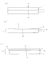
- FIG. 1A is a schematic diagram showing a state in which a silicon substrate 1 is formed on a polycrystalline ceramic substrate
- FIG. 1B is a schematic diagram showing a base substrate 7
- FIG. FIG. 3 is a schematic diagram showing a seed crystal substrate 8.
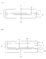
- FIG. 2A is a schematic diagram illustrating the composite substrate 9
- FIG. 2B is a schematic diagram illustrating the light emitting element 10.
- the silicon substrate 1 is directly bonded to the polycrystalline ceramic substrate 2.
- 1b is a bonding surface of the silicon substrate to the polycrystalline ceramic substrate, 1a is an exposed main surface, and 7 is an exposed side surface.
- the silicon substrate 1 is thinned to form a thinned silicon substrate 1A.
- 1c is a processed surface of the thinned silicon substrate, and 7A is an exposed side surface.
- a base substrate 7 is formed by the silicon substrate 1 ⁇ / b> A and the polycrystalline ceramic substrate 2.
- the seed crystal film 3 is formed on the processed surface 1c of the silicon substrate 1A, and the seed crystal substrate 8 is obtained.
- a gallium nitride crystal layer 4 is formed on the seed crystal film 3 by a flux method to obtain a GaN template substrate (composite substrate) 9.
- the light emitting element structure 5 is formed on the GaN template substrate 9 to obtain the functional element 10 (FIG. 2B).
- Examples of the polycrystalline ceramic substrate 2 include alumina and aluminum nitride.
- the bonding method of the polycrystalline ceramic substrate and the silicon substrate can be directly bonded by, for example, polishing both substrates, irradiating with an argon beam, bringing the polished surfaces into contact with each other in a vacuum and applying a load.
- the thickness it is preferable to reduce the thickness to, for example, 8 ⁇ m or less by thinning the silicon substrate.
- a polishing process is preferable.
- the thickness of the silicon substrate after the thinning process is preferably 8 ⁇ m or less, more preferably 3 ⁇ m or less.
- the thickness of the thinned silicon substrate is usually 0.2 ⁇ m or more, and preferably 0.5 ⁇ m or more.
- the thickness of the silicon substrate is preferably 30 ⁇ m or less.
- the seed crystal film is formed on the silicon substrate, it is also possible to cover the side surface of the silicon substrate with the seed crystal film to prevent the silicon substrate from being exposed.
- a seed crystal film made of a group 13 element nitride is provided on a silicon substrate by a vapor phase method.
- the seed crystal film may be a single layer or may include a buffer layer on the base substrate side.
- a vapor phase growth method can be cited, and a metal organic chemical vapor deposition (MOCVD) method, a hydride vapor deposition (HVPE) method, a pulse excitation deposition ( PXD) method, MBE method, and sublimation method.
- MOCVD metal organic chemical vapor deposition
- HVPE hydride vapor deposition
- PXD pulse excitation deposition
- MBE method MBE method
- sublimation method sublimation method.
- the MOCVD method is particularly preferable.
- the group 13 element is a group 13 element according to the periodic table established by IUPAC.
- the group 13 element is specifically gallium, aluminum, indium, thallium, or the like.
- the additive include carbon, low melting point metals (tin, bismuth, silver, gold) and high melting point metals (transition metals such as iron, manganese, titanium, and chromium).
- the low melting point metal may be added for the purpose of preventing oxidation of sodium, and the high melting point metal may be mixed from a container in which a crucible is put or a heater of a growth furnace.
- the group 13 element nitride is preferably GaN, AlN, GaAlN, GaInN, AlInN, or GaAlInN.
- a gallium nitride crystal layer is formed on the seed crystal film by a flux method.
- the type of flux is not particularly limited as long as a gallium nitride crystal can be generated.
- a flux containing at least one of an alkali metal and an alkaline earth metal is used, and a flux containing sodium is particularly preferred.
- gallium raw material is mixed and used for the flux.
- gallium source material gallium simple substance, gallium alloy, and gallium compound can be applied, but gallium simple substance is also preferable in terms of handling.
- the growth temperature of the gallium nitride crystal in the flux method and the holding time during the growth are not particularly limited, and are appropriately changed according to the composition of the flux.
- the growth temperature is preferably 800 to 950 ° C., and more preferably 850 to 900 ° C.
- single crystals are grown in an atmosphere containing a gas containing nitrogen atoms.
- This gas is preferably nitrogen gas, but may be ammonia.
- the pressure of the atmosphere is not particularly limited, but is preferably 10 atm or more, and more preferably 30 atm or more from the viewpoint of preventing evaporation of the flux. However, since the apparatus becomes large when the pressure is high, the total pressure of the atmosphere is preferably 2000 atmospheres or less, and more preferably 500 atmospheres or less.
- the gas other than the gas containing nitrogen atoms in the atmosphere is not limited, but an inert gas is preferable, and argon, helium, and neon are particularly preferable.
- a functional layer is formed on the composite substrate thus obtained by a vapor phase method.
- a semiconductor light emitting diode LED
- MOCVD method a semiconductor light emitting diode
- the film forming temperature of the functional layer is preferably 1000 ° C. or higher, more preferably 1050 ° C. or higher, from the viewpoint of crystal quality. Further, from the viewpoint of not deteriorating the crystal quality of the gallium nitride crystal layer, the film forming temperature of the functional layer is preferably 1200 ° C. or lower, and more preferably 1150 ° C. or lower.
- the material of the functional layer is preferably a group 13 element nitride.
- the group 13 element is a group 13 element according to the periodic table established by IUPAC.
- the group 13 element is specifically gallium, aluminum, indium, thallium, or the like.
- Examples of the additive include carbon and transition metals (iron, manganese, titanium, chromium, etc.).
- the light-emitting element structure includes, for example, an n-type semiconductor layer, a light-emitting region provided on the n-type semiconductor layer, and a p-type semiconductor layer provided on the light-emitting region.
- an n-type contact layer, an n-type cladding layer, an active layer, a p-type cladding layer, and a p-type contact layer are formed on a gallium nitride crystal layer to constitute a light emitting element structure.
- the present invention can be used in technical fields that are required to have high quality, such as high color rendering high-intensity white LEDs, blue-violet lasers for high-speed and high-density optical disks, and power devices used in inverters for hybrid vehicles.
- a polycrystalline ceramic substrate 2 made of aluminum nitride having a diameter of 4 inches and a thickness of 500 ⁇ m was prepared, and planarized by polishing with diamond abrasive grains.
- the polished surface was observed in an area of 10 ⁇ m ⁇ with an atomic force microscope (AFM), and the surface roughness was measured.
- the root mean square roughness was 0.8 nm.
- the polished polycrystalline ceramic substrate 2 made of aluminum nitride and the (111) -plane silicon substrate 1 having a diameter of 4 inches and a thickness of 300 ⁇ m polished on both sides are placed in a vacuum chamber. Argon beam irradiation was performed for 3 minutes. Thereafter, the irradiated surfaces were brought into contact with each other in a vacuum chamber, and bonded by applying a load of 1 ton at room temperature to obtain a composite wafer.
- the silicon surface of the composite wafer 7 was polished with diamond abrasive grains.
- the silicon was polished to a thickness of 5 ⁇ m to form a thin film, and then the wafer was chamfered by a beveling process. Tapering was performed by beveling so that the silicon surface was 0.5 mm inside from the outer periphery of the polycrystalline ceramic substrate.
- the polished surface of the silicon surface was observed with an AFM in an area of 10 ⁇ m ⁇ and the surface roughness was measured, the root mean square roughness was 0.1 nm or less.
- the reactor internal pressure was 10 kPa
- TMA bubbling gas was introduced into the reactor at a predetermined flow rate ratio, and NH 3 and TMA were reacted to form an AlN film with a thickness of 100 nm. Thereafter, NH 3 , TMA and TMG were reacted to form an AlGaN film with a thickness of 40 nm.
- the GaN film 3 was grown to a thickness of 3 ⁇ m using TMG (trimethylgallium) and ammonia as raw materials. Thereafter, the substrate temperature was lowered to room temperature, and the composite wafer was taken out.
- TMG trimethylgallium
- the GaN crystal layer 4 was grown by the flux method.
- the raw materials used for the growth are gallium, sodium and lithium.
- the seed crystal substrate was placed in an alumina crucible so that the flux was in contact with the GaN film formed by the MOCVD method.
- the crucible was filled with 30 g of gallium, 44 g of sodium, and 30 mg of lithium, respectively, and a GaN single crystal was grown for about 10 hours at a furnace temperature of 900 ° C. and a pressure of 5 MPa.
- a GaN single crystal was deposited on the substrate surface with a thickness of about 100 ⁇ m.
- the dislocation density of the gallium nitride single crystal film was calculated by counting dark spots (points that appear darker than the surroundings due to weak light emission) as dislocations appearing on the substrate surface by the CL (cathode luminescence) method.
- CL cathode luminescence
- S-3400N Type II manufactured by Hitachi High-Technologies Corporation equipped with a cathodoluminescence detector was used. As a result, the dislocation density was about 7 ⁇ 10 6 cm ⁇ 2 .
- the light-emitting element structure 5 was formed on the composite substrate 9 of 4 inch diameter gallium nitride single crystal obtained above.
- the composite substrate 9 is again placed in the MOCVD furnace, the substrate temperature is raised to 1100 ° C. in a hydrogen / nitrogen mixed atmosphere, and the n-type GaN film is 1 ⁇ m thick using TMG (trimethylgallium) and ammonia as raw materials and silane gas as a dopant. I grew up.
- TMG trimethylgallium
- the temperature was decreased to 750 ° C. to form three pairs of InGaN / GaN quantum well structures.
- the substrate temperature was raised to 1050 ° C., and a p-type GaN film was grown to a thickness of 0.1 ⁇ m using TMG (trimethylgallium) and ammonia as raw materials and Cp 2 Mg as a dopant.
Landscapes
- Chemical & Material Sciences (AREA)
- Organic Chemistry (AREA)
- Engineering & Computer Science (AREA)
- Crystallography & Structural Chemistry (AREA)
- Materials Engineering (AREA)
- Metallurgy (AREA)
- Chemical Kinetics & Catalysis (AREA)
- General Chemical & Material Sciences (AREA)
- Inorganic Chemistry (AREA)
- Crystals, And After-Treatments Of Crystals (AREA)
- Chemical Vapour Deposition (AREA)
- Liquid Deposition Of Substances Of Which Semiconductor Devices Are Composed (AREA)
- Recrystallisation Techniques (AREA)
Abstract
Description
液相法の一種であるフラックス法により転位密度の低い窒化物ガリウム単結晶基板を得ることが出来る。フラックス法によるGaN単結晶成長では、一般的に種結晶を用い、そこを起点としてGaNを成長させる。成長用の基板はサファイア基板上にMOCVD法やHVPE法などの気相法により1~20μm程度の種結晶層を成長させたウェハー(種結晶基板)を用いる(特許文献1)。
従来のサファイア基板に代わり、シリコン基板上に窒化物半導体を有機金属化学気相成長(MOCVD)法により成膜し、パワーデバイス構造やLED素子構造を形成するということも盛んに行われるようになってきた。シリコン基板は大きなサイズのウェハーが入手できるメリットがある。
青色LED,青紫色半導体レーザー及びパワー半導体などの半導体デバイスの製作に、窒化ガリウムなどのIII族窒化物からなる基板と下地基板とを貼り合わせた複合基板を用いることができる(特許文献2)。
(1) 多結晶セラミック基板、前記多結晶セラミック基板に対して直接接合されているシリコン基板、前記シリコン基板上に気相法によって設けられた13族元素窒化物からなる種結晶膜、およびこの種結晶膜上にフラックス法によって結晶成長した窒化ガリウム結晶層を備えることを特徴とする、複合基板。
(2) 前記13族元素窒化物が窒化ガリウムであることを特徴とする、(1)の複合基板。
(3) 前記多結晶セラミック基板が、アルミナあるいは窒化アルミニウムからなる(1)~(2)記載の複合基板。
(4) 前記シリコン基板が薄層化されていることを特徴とする、(1)~(3)の複合基板。
(5) 前記シリコン基板は、0.2ミクロン以上、8ミクロン以下の厚さに薄層化されていることを特徴とする(4)記載の複合基板。
(6) (1)~(5)のいずれかに記載の複合基板、および前記窒化ガリウム結晶層上に気相法によって形成された13族元素窒化物からなる機能層を備えていることを特徴とする、機能素子。
(7) 前記機能層が発光機能を有することを特徴とする、(6)の機能素子。
前記種結晶膜上に窒化ガリウム結晶層をフラックス法によって育成する工程;
を有することを特徴とする、複合基板の製造方法。
(9) 前記13族元素窒化物が窒化ガリウムであることを特徴とする、(8)の方法。
(10) 前記多結晶セラミック基板が、アルミナあるいは窒化アルミニウムからなる、(8)または(9)記載の方法。
(11) 前記シリコン基板を薄層化する工程を有することを特徴とする、(8)~(10)の方法。
(12) 前記シリコン基板を0.2ミクロン以上、8ミクロン以下の厚さに薄層化する工程を有することを特徴とする、(11)記載の方法。
(13) 多結晶セラミック基板、前記多結晶セラミック基板に対して直接接合されているシリコン基板、および前記シリコン基板上に気相法によって設けられた13族元素窒化物からなる種結晶膜を備えることを特徴とする、種結晶基板。
(14) 前記13族元素窒化物が窒化ガリウムであることを特徴とする、(13)の種結晶基板。
(15) 前記多結晶セラミック基板が、アルミナあるいは窒化アルミニウムからなる、(13)または(14)記載の種結晶基板。
(16) 前記シリコン基板が薄層化されていることを特徴とする、(13)~(15)の種結晶基板。
(17) 前記シリコン基板は、0.2ミクロン以上、8ミクロン以下の厚さに薄層化されていることを特徴とする(16)記載の種結晶基板。
種結晶膜は、一層であってよく、あるいは下地基板側にバッファ層を含んでいて良い。種結晶膜の形成方法は気相成長法を好ましい一例として挙げることができ、有機金属化学気相成長(MOCVD: Metal Organic Chemical Vapor Deposition)法、ハイドライド気相成長(HVPE)法、パルス励起堆積(PXD)法、MBE法、昇華法を例示できる。MOCVD法が特に好ましい。
複合基板上に気相法、好ましくはMOCVD法により半導体発光ダイオード(LED)を作製すると、LED内部の転位密度がGaNテンプレートのGaN単結晶とほぼ同じ密度となることから、高輝度化やドループ現象の抑制が可能となる。
直径4インチ500μm厚の窒化アルミニウムからなる多結晶セラミック基板2を用意し、ダイヤモンド砥粒を用いて研磨することにより平坦化した。研磨した表面を原子間力顕微鏡(AFM)にて10μm□の領域で観察し、表面粗さを計測したところ、二乗平均粗さで0.8nmであった。
下地基板7に対して、フッ化水素酸/純水=1/10(体積比)なる組成の希フッ酸による希フッ酸洗浄により表面酸化膜を除去した状態とし、これをMOCVD装置のリアクタ内サセプターにセットした。この際、シリコン面に成膜されるように、多結晶セラミック基板2側がサセプターに接するようにした。次いで、リアクタ内を水素・窒素混合雰囲気とし、基板温度が初期層形成温度である1050℃となるまで加熱した。
この複合ウェハーを種結晶基板8としてフラックス法にてGaN結晶層4を育成した。成長に用いた原料は、ガリウム、ナトリウムおよびリチウムである。MOCVD法により成膜したGaN膜にフラックスが接するように種結晶基板をアルミナるつぼに配置した。このるつぼにガリウム30g、ナトリウム44g、リチウム30mgをそれぞれ充填して、炉内温度900℃・圧力5MPaにてGaN単結晶を約10時間育成した。るつぼから種結晶基板8を取り出したところ、基板表面にGaN単結晶が約100μmの厚さで堆積していた。
上記で得られた直径4インチ窒化ガリウム単結晶の複合基板9の上に発光素子構造5を成膜した。
シリコン基板1として直径4インチ300μm厚の(111)面を使用するが、薄層化研磨加工は行わず、シリコン基板1上にそのまま種結晶膜3を形成した(比較例1)。また、シリコン基板1として直径4インチ500μm厚の(111)面シリコン基板を使用するが、多結晶セラミック基板2を用いず、基板の複合化も行わなかった(比較例2)。その他は上記の実施例と同様にして複合基板の作製を試みた。
Claims (17)
- 多結晶セラミック基板、前記多結晶セラミック基板に対して直接接合されているシリコン基板、前記シリコン基板上に気相法によって設けられた13族元素窒化物からなる種結晶膜、およびこの種結晶膜上にフラックス法によって結晶成長した窒化ガリウム結晶層を備えることを特徴とする、複合基板。
- 前記13族元素窒化物が窒化ガリウムであることを特徴とする、請求項1記載の複合基板。
- 前記多結晶セラミック基板が、アルミナあるいは窒化アルミニウムからなる、請求項1または2記載の複合基板。
- 前記シリコン基板が薄層化されていることを特徴とする、請求項1~3のいずれか一つの請求項に記載の複合基板。
- 前記シリコン基板は、0.2ミクロン以上、8ミクロン以下の厚さに薄層化されていることを特徴とする、請求項4記載の複合基板。
- 請求項1~5のいずれか一つの請求項に記載の複合基板、および前記窒化ガリウム結晶層上に気相法によって形成された13族元素窒化物からなる機能層を備えていることを特徴とする、機能素子。
- 前記機能層が発光機能を有することを特徴とする、請求項6記載の機能素子。
- 多結晶セラミック基板とシリコン基板とを直接接合してなる複合基板の前記シリコン基板上に、13族元素窒化物からなる種結晶膜を気相法によって成膜する工程;および
前記種結晶膜上に窒化ガリウム結晶層をフラックス法によって育成する工程;
を有することを特徴とする、複合基板の製造方法。 - 前記13族元素窒化物が窒化ガリウムであることを特徴とする、請求項8記載の方法。
- 前記多結晶セラミック基板が、アルミナあるいは窒化アルミニウムからなる、請求項8または9記載の方法。
- 前記シリコン基板を薄層化する工程を有することを特徴とする、請求項8~10のいずれか一つの請求項に記載の方法。
- 前記シリコン基板を、0.2ミクロン以上、8ミクロン以下の厚さに薄層化する工程を有することを特徴とする、請求項11記載の方法。
- 多結晶セラミック基板、前記多結晶セラミック基板に対して直接接合されているシリコン基板、および前記シリコン基板上に気相法によって設けられた13族元素窒化物からなる種結晶膜を備えることを特徴とする、種結晶基板。
- 前記13族元素窒化物が窒化ガリウムであることを特徴とする、請求項13記載の種結晶基板。
- 前記多結晶セラミック基板が、アルミナあるいは窒化アルミニウムからなる、請求項13または14記載の種結晶基板。
- 前記シリコン基板が薄層化されていることを特徴とする、請求項13~15のいずれか一つの請求項に記載の種結晶基板。
- 前記シリコン基板は、0.2ミクロン以上、8ミクロン以下の厚さに薄層化されていることを特徴とする、請求項16記載の種結晶基板。
Priority Applications (4)
| Application Number | Priority Date | Filing Date | Title |
|---|---|---|---|
| CN201480034478.4A CN105393336B (zh) | 2013-07-22 | 2014-07-18 | 复合基板、其制造方法、功能元件以及晶种基板 |
| KR1020157034889A KR101590309B1 (ko) | 2013-07-22 | 2014-07-18 | 복합 기판, 그 제조 방법, 기능 소자 및 종결정 기판 |
| JP2015522823A JP5805352B2 (ja) | 2013-07-22 | 2014-07-18 | 複合基板、その製造方法、機能素子および種結晶基板 |
| US14/969,809 US10030318B2 (en) | 2013-07-22 | 2015-12-15 | Composite substrate, method for fabricating same, function element, and seed crystal substrate |
Applications Claiming Priority (2)
| Application Number | Priority Date | Filing Date | Title |
|---|---|---|---|
| US201361856797P | 2013-07-22 | 2013-07-22 | |
| US61/856,797 | 2013-07-22 |
Related Child Applications (1)
| Application Number | Title | Priority Date | Filing Date |
|---|---|---|---|
| US14/969,809 Continuation US10030318B2 (en) | 2013-07-22 | 2015-12-15 | Composite substrate, method for fabricating same, function element, and seed crystal substrate |
Publications (1)
| Publication Number | Publication Date |
|---|---|
| WO2015012218A1 true WO2015012218A1 (ja) | 2015-01-29 |
Family
ID=52393259
Family Applications (1)
| Application Number | Title | Priority Date | Filing Date |
|---|---|---|---|
| PCT/JP2014/069174 Ceased WO2015012218A1 (ja) | 2013-07-22 | 2014-07-18 | 複合基板、その製造方法、機能素子および種結晶基板 |
Country Status (6)
| Country | Link |
|---|---|
| US (1) | US10030318B2 (ja) |
| JP (1) | JP5805352B2 (ja) |
| KR (1) | KR101590309B1 (ja) |
| CN (1) | CN105393336B (ja) |
| TW (1) | TWI510667B (ja) |
| WO (1) | WO2015012218A1 (ja) |
Cited By (2)
| Publication number | Priority date | Publication date | Assignee | Title |
|---|---|---|---|---|
| JP2020504447A (ja) * | 2016-12-28 | 2020-02-06 | クロミス,インコーポレイテッド | 縦型パワーデバイスのための方法およびシステム |
| JPWO2023157547A1 (ja) * | 2022-02-17 | 2023-08-24 |
Families Citing this family (7)
| Publication number | Priority date | Publication date | Assignee | Title |
|---|---|---|---|---|
| US20140127857A1 (en) * | 2012-11-07 | 2014-05-08 | Taiwan Semiconductor Manufacturing Company, Ltd. | Carrier Wafers, Methods of Manufacture Thereof, and Packaging Methods |
| CN105591004B (zh) * | 2016-03-29 | 2020-07-10 | 苏州晶湛半导体有限公司 | 基于图形化Si衬底的LED外延片及其制备方法 |
| TWI708303B (zh) * | 2018-02-22 | 2020-10-21 | 國立大學法人大阪大學 | 基板評價用晶片及基板評價裝置 |
| TWI749928B (zh) * | 2020-12-01 | 2021-12-11 | 合晶科技股份有限公司 | 複合基板結構及其製造方法 |
| CN219246703U (zh) * | 2022-12-06 | 2023-06-23 | 苏州晶湛半导体有限公司 | 一种复合衬底、外延片及半导体器件 |
| EP4632118A1 (en) * | 2024-04-09 | 2025-10-15 | SiCrystal GmbH | Layered substrate, method of fabrication of a layered substrate and method for growing an epitaxial layer with the layered substrate |
| EP4632116A1 (en) * | 2024-04-09 | 2025-10-15 | SiCrystal GmbH | Layered seed, method of fabrication of a layered seed and method for growing a volume mono crystal with the layered seed |
Citations (4)
| Publication number | Priority date | Publication date | Assignee | Title |
|---|---|---|---|---|
| JP2007290924A (ja) * | 2006-04-26 | 2007-11-08 | Toyoda Gosei Co Ltd | 電子デバイス用半導体基板、その製造方法、電子デバイス、及び電界効果トランジスタ |
| WO2010084675A1 (ja) * | 2009-01-21 | 2010-07-29 | 日本碍子株式会社 | 3b族窒化物結晶板 |
| JP2012124473A (ja) * | 2010-11-15 | 2012-06-28 | Ngk Insulators Ltd | 複合基板及び複合基板の製造方法 |
| WO2013022122A1 (ja) * | 2011-08-10 | 2013-02-14 | 日本碍子株式会社 | 13族元素窒化物膜およびその積層体 |
Family Cites Families (8)
| Publication number | Priority date | Publication date | Assignee | Title |
|---|---|---|---|---|
| US6497763B2 (en) * | 2001-01-19 | 2002-12-24 | The United States Of America As Represented By The Secretary Of The Navy | Electronic device with composite substrate |
| US6897138B2 (en) * | 2001-06-25 | 2005-05-24 | Toyoda Gosei Co., Ltd. | Method and apparatus for producing group III nitride compound semiconductor |
| US20030089950A1 (en) * | 2001-11-15 | 2003-05-15 | Kuech Thomas F. | Bonding of silicon and silicon-germanium to insulating substrates |
| GB2398672A (en) * | 2003-02-19 | 2004-08-25 | Qinetiq Ltd | Group IIIA nitride buffer layers |
| US7687827B2 (en) * | 2004-07-07 | 2010-03-30 | Nitronex Corporation | III-nitride materials including low dislocation densities and methods associated with the same |
| JP2007214256A (ja) * | 2006-02-08 | 2007-08-23 | Toshiba Ceramics Co Ltd | Soiウェーハ |
| JP4958207B2 (ja) * | 2006-03-16 | 2012-06-20 | 豊田合成株式会社 | 光素子基板の製造方法 |
| TW200741044A (en) | 2006-03-16 | 2007-11-01 | Toyoda Gosei Kk | Semiconductor substrate, electronic device, optical device, and production methods therefor |
-
2014
- 2014-07-18 KR KR1020157034889A patent/KR101590309B1/ko not_active Expired - Fee Related
- 2014-07-18 WO PCT/JP2014/069174 patent/WO2015012218A1/ja not_active Ceased
- 2014-07-18 JP JP2015522823A patent/JP5805352B2/ja not_active Expired - Fee Related
- 2014-07-18 CN CN201480034478.4A patent/CN105393336B/zh not_active Expired - Fee Related
- 2014-07-21 TW TW103124879A patent/TWI510667B/zh not_active IP Right Cessation
-
2015
- 2015-12-15 US US14/969,809 patent/US10030318B2/en active Active
Patent Citations (4)
| Publication number | Priority date | Publication date | Assignee | Title |
|---|---|---|---|---|
| JP2007290924A (ja) * | 2006-04-26 | 2007-11-08 | Toyoda Gosei Co Ltd | 電子デバイス用半導体基板、その製造方法、電子デバイス、及び電界効果トランジスタ |
| WO2010084675A1 (ja) * | 2009-01-21 | 2010-07-29 | 日本碍子株式会社 | 3b族窒化物結晶板 |
| JP2012124473A (ja) * | 2010-11-15 | 2012-06-28 | Ngk Insulators Ltd | 複合基板及び複合基板の製造方法 |
| WO2013022122A1 (ja) * | 2011-08-10 | 2013-02-14 | 日本碍子株式会社 | 13族元素窒化物膜およびその積層体 |
Cited By (5)
| Publication number | Priority date | Publication date | Assignee | Title |
|---|---|---|---|---|
| JP2020504447A (ja) * | 2016-12-28 | 2020-02-06 | クロミス,インコーポレイテッド | 縦型パワーデバイスのための方法およびシステム |
| JP7118069B2 (ja) | 2016-12-28 | 2022-08-15 | クロミス,インコーポレイテッド | 縦型パワーデバイスのための方法およびシステム |
| JPWO2023157547A1 (ja) * | 2022-02-17 | 2023-08-24 | ||
| WO2023157547A1 (ja) * | 2022-02-17 | 2023-08-24 | 日本碍子株式会社 | Iii族元素窒化物半導体基板および貼り合わせ基板 |
| JP7855673B2 (ja) | 2022-02-17 | 2026-05-08 | Ngk株式会社 | Iii族元素窒化物半導体基板および貼り合わせ基板 |
Also Published As
| Publication number | Publication date |
|---|---|
| JP5805352B2 (ja) | 2015-11-04 |
| TWI510667B (zh) | 2015-12-01 |
| KR101590309B1 (ko) | 2016-01-29 |
| US20160108552A1 (en) | 2016-04-21 |
| US10030318B2 (en) | 2018-07-24 |
| KR20160003289A (ko) | 2016-01-08 |
| JPWO2015012218A1 (ja) | 2017-03-02 |
| CN105393336A (zh) | 2016-03-09 |
| TW201520357A (zh) | 2015-06-01 |
| CN105393336B (zh) | 2017-10-31 |
Similar Documents
| Publication | Publication Date | Title |
|---|---|---|
| JP5805352B2 (ja) | 複合基板、その製造方法、機能素子および種結晶基板 | |
| JP3352712B2 (ja) | 窒化ガリウム系半導体素子及びその製造方法 | |
| US8882910B2 (en) | AlGaN substrate and production method thereof | |
| US7125801B2 (en) | Method of manufacturing Group III nitride crystal substrate, etchant used in the method, Group III nitride crystal substrate, and semiconductor device including the same | |
| US20120178215A1 (en) | Nitride Crystal with Removable Surface Layer and Methods of Manufacture | |
| TW201031027A (en) | Method for manufacturing light emitting device | |
| TW200901513A (en) | Method for producing group III nitride semiconductor light emitting device, group III nitride semiconductor light emitting device, and lamp | |
| JP6117199B2 (ja) | 半導体基板及び形成する方法 | |
| US9287453B2 (en) | Composite substrates and functional device | |
| JP6579951B2 (ja) | 窒化アルミニウム単結晶積層体、該積層体の製造方法、及び該積層体を利用した半導体素子の製造方法 | |
| CN103732809A (zh) | 13族元素氮化物膜的剥离方法 | |
| JP4486435B2 (ja) | Iii族窒化物結晶基板の製造方法、それに用いるエッチング液 | |
| CN107002283B (zh) | 13族元素氮化物结晶基板及功能元件 | |
| JP6117821B2 (ja) | 複合基板および機能素子 | |
| CN108291329A (zh) | 13 族元素氮化物结晶基板及功能元件 | |
| CN117460868A (zh) | 紫外线发光元件用外延片及其制造方法 | |
| JP2008053372A (ja) | 半導体デバイスの製造方法 | |
| CN107002286A (zh) | 13族元素氮化物结晶层及功能元件 | |
| WO2004067814A1 (ja) | Iii族元素窒化物単結晶の製造方法およびそれにより得られたiii族元素窒化物透明単結晶 |
Legal Events
| Date | Code | Title | Description |
|---|---|---|---|
| WWE | Wipo information: entry into national phase |
Ref document number: 201480034478.4 Country of ref document: CN |
|
| 121 | Ep: the epo has been informed by wipo that ep was designated in this application |
Ref document number: 14828936 Country of ref document: EP Kind code of ref document: A1 |
|
| ENP | Entry into the national phase |
Ref document number: 2015522823 Country of ref document: JP Kind code of ref document: A |
|
| ENP | Entry into the national phase |
Ref document number: 20157034889 Country of ref document: KR Kind code of ref document: A |
|
| NENP | Non-entry into the national phase |
Ref country code: DE |
|
| 122 | Ep: pct application non-entry in european phase |
Ref document number: 14828936 Country of ref document: EP Kind code of ref document: A1 |