WO2015004945A1 - 蒸着装置、蒸着方法、及び、有機エレクトロルミネッセンス素子の製造方法 - Google Patents
蒸着装置、蒸着方法、及び、有機エレクトロルミネッセンス素子の製造方法 Download PDFInfo
- Publication number
- WO2015004945A1 WO2015004945A1 PCT/JP2014/055407 JP2014055407W WO2015004945A1 WO 2015004945 A1 WO2015004945 A1 WO 2015004945A1 JP 2014055407 W JP2014055407 W JP 2014055407W WO 2015004945 A1 WO2015004945 A1 WO 2015004945A1
- Authority
- WO
- WIPO (PCT)
- Prior art keywords
- vapor deposition
- opening
- space
- plate portion
- substrate
- Prior art date
- Legal status (The legal status is an assumption and is not a legal conclusion. Google has not performed a legal analysis and makes no representation as to the accuracy of the status listed.)
- Ceased
Links
Images









Classifications
-
- C—CHEMISTRY; METALLURGY
- C23—COATING METALLIC MATERIAL; COATING MATERIAL WITH METALLIC MATERIAL; CHEMICAL SURFACE TREATMENT; DIFFUSION TREATMENT OF METALLIC MATERIAL; COATING BY VACUUM EVAPORATION, BY SPUTTERING, BY ION IMPLANTATION OR BY CHEMICAL VAPOUR DEPOSITION, IN GENERAL; INHIBITING CORROSION OF METALLIC MATERIAL OR INCRUSTATION IN GENERAL
- C23C—COATING METALLIC MATERIAL; COATING MATERIAL WITH METALLIC MATERIAL; SURFACE TREATMENT OF METALLIC MATERIAL BY DIFFUSION INTO THE SURFACE, BY CHEMICAL CONVERSION OR SUBSTITUTION; COATING BY VACUUM EVAPORATION, BY SPUTTERING, BY ION IMPLANTATION OR BY CHEMICAL VAPOUR DEPOSITION, IN GENERAL
- C23C14/00—Coating by vacuum evaporation, by sputtering or by ion implantation of the coating forming material
- C23C14/04—Coating on selected surface areas, e.g. using masks
- C23C14/042—Coating on selected surface areas, e.g. using masks using masks
-
- C—CHEMISTRY; METALLURGY
- C23—COATING METALLIC MATERIAL; COATING MATERIAL WITH METALLIC MATERIAL; CHEMICAL SURFACE TREATMENT; DIFFUSION TREATMENT OF METALLIC MATERIAL; COATING BY VACUUM EVAPORATION, BY SPUTTERING, BY ION IMPLANTATION OR BY CHEMICAL VAPOUR DEPOSITION, IN GENERAL; INHIBITING CORROSION OF METALLIC MATERIAL OR INCRUSTATION IN GENERAL
- C23C—COATING METALLIC MATERIAL; COATING MATERIAL WITH METALLIC MATERIAL; SURFACE TREATMENT OF METALLIC MATERIAL BY DIFFUSION INTO THE SURFACE, BY CHEMICAL CONVERSION OR SUBSTITUTION; COATING BY VACUUM EVAPORATION, BY SPUTTERING, BY ION IMPLANTATION OR BY CHEMICAL VAPOUR DEPOSITION, IN GENERAL
- C23C14/00—Coating by vacuum evaporation, by sputtering or by ion implantation of the coating forming material
- C23C14/06—Coating by vacuum evaporation, by sputtering or by ion implantation of the coating forming material characterised by the coating material
- C23C14/12—Organic material
-
- C—CHEMISTRY; METALLURGY
- C23—COATING METALLIC MATERIAL; COATING MATERIAL WITH METALLIC MATERIAL; CHEMICAL SURFACE TREATMENT; DIFFUSION TREATMENT OF METALLIC MATERIAL; COATING BY VACUUM EVAPORATION, BY SPUTTERING, BY ION IMPLANTATION OR BY CHEMICAL VAPOUR DEPOSITION, IN GENERAL; INHIBITING CORROSION OF METALLIC MATERIAL OR INCRUSTATION IN GENERAL
- C23C—COATING METALLIC MATERIAL; COATING MATERIAL WITH METALLIC MATERIAL; SURFACE TREATMENT OF METALLIC MATERIAL BY DIFFUSION INTO THE SURFACE, BY CHEMICAL CONVERSION OR SUBSTITUTION; COATING BY VACUUM EVAPORATION, BY SPUTTERING, BY ION IMPLANTATION OR BY CHEMICAL VAPOUR DEPOSITION, IN GENERAL
- C23C16/00—Chemical coating by decomposition of gaseous compounds, without leaving reaction products of surface material in the coating, i.e. chemical vapour deposition [CVD] processes
- C23C16/44—Chemical coating by decomposition of gaseous compounds, without leaving reaction products of surface material in the coating, i.e. chemical vapour deposition [CVD] processes characterised by the method of coating
- C23C16/458—Chemical coating by decomposition of gaseous compounds, without leaving reaction products of surface material in the coating, i.e. chemical vapour deposition [CVD] processes characterised by the method of coating characterised by the method used for supporting substrates in the reaction chamber
-
- H—ELECTRICITY
- H10—SEMICONDUCTOR DEVICES; ELECTRIC SOLID-STATE DEVICES NOT OTHERWISE PROVIDED FOR
- H10K—ORGANIC ELECTRIC SOLID-STATE DEVICES
- H10K71/00—Manufacture or treatment specially adapted for the organic devices covered by this subclass
- H10K71/10—Deposition of organic active material
- H10K71/16—Deposition of organic active material using physical vapour deposition [PVD], e.g. vacuum deposition or sputtering
- H10K71/166—Deposition of organic active material using physical vapour deposition [PVD], e.g. vacuum deposition or sputtering using selective deposition, e.g. using a mask
-
- H—ELECTRICITY
- H10—SEMICONDUCTOR DEVICES; ELECTRIC SOLID-STATE DEVICES NOT OTHERWISE PROVIDED FOR
- H10K—ORGANIC ELECTRIC SOLID-STATE DEVICES
- H10K50/00—Organic light-emitting devices
-
- H—ELECTRICITY
- H10—SEMICONDUCTOR DEVICES; ELECTRIC SOLID-STATE DEVICES NOT OTHERWISE PROVIDED FOR
- H10K—ORGANIC ELECTRIC SOLID-STATE DEVICES
- H10K50/00—Organic light-emitting devices
- H10K50/10—OLEDs or polymer light-emitting diodes [PLED]
- H10K50/11—OLEDs or polymer light-emitting diodes [PLED] characterised by the electroluminescent [EL] layers
-
- H—ELECTRICITY
- H10—SEMICONDUCTOR DEVICES; ELECTRIC SOLID-STATE DEVICES NOT OTHERWISE PROVIDED FOR
- H10K—ORGANIC ELECTRIC SOLID-STATE DEVICES
- H10K59/00—Integrated devices, or assemblies of multiple devices, comprising at least one organic light-emitting element covered by group H10K50/00
- H10K59/10—OLED displays
Definitions
- first electrode / positive Hole injection layer / hole transport layer / electron injection layer / electron injection layer / electron injection layer / electron injection layer / second electrode (2) First electrode / hole transport layer / light emitting layer / electron transport layer / second electrode (3) First electrode / hole transport layer / light emitting layer / Hole blocking layer / electron transport layer / second electrode (4) first electrode / hole transport layer / light emitting layer / hole blocking layer / electron transport layer / electron injection layer / second electrode (5) first electrode / Hole injection layer / hole transport layer / light emitting layer / electron transport layer / electron injection layer / second electrode (6) first electrode / hole injection layer / hole transport layer / light emitting layer / hole blocking layer / electron Transport layer / second electrode (7) first electrode / hole injection layer / hole transport layer / light emitting layer / hole blocking layer / electron transport layer / electron injection layer / second electrode (8) first electrode / positive Hole injection layer / hole transport layer / electron transport layer
- a photosensitive resin is applied on the insulating substrate 11 on which the TFTs 12, the wirings 14 and the like are formed by a general method, and patterning is performed on the insulating substrate 11 by photolithography.
- An interlayer film 13 is formed.
- a resin such as an acrylic resin or a polyimide resin can be used as a material of the interlayer film 13.
- the acrylic resin include Optomer series manufactured by JSR Corporation.
- a polyimide resin the photo nice series by Toray Industries, Inc. is mentioned, for example.
- the polyimide resin is generally not transparent but colored. Therefore, when a bottom emission type organic EL display device is manufactured as the organic EL display device 1 as shown in FIG. 3, a transparent resin such as an acrylic resin is more preferably used as the interlayer film 13. .
- the ITO film is etched using ferric chloride as an etchant. Thereafter, the photoresist is stripped using a resist stripping solution, and substrate cleaning is further performed. As a result, the first electrodes 21 are formed in a matrix on the interlayer film 13.
- the electron transport layer 24 is covered with the hole injection layer / hole transport layer 22 and the light emitting layers 23R, 23G, and 23B. Vapor deposition is performed on the entire display area of the TFT substrate 10 (S4).
- the electron injection layer 25 is deposited on the entire display region of the TFT substrate 10 so as to cover the electron transport layer 24 by the same method as in the hole injection layer / hole transport layer deposition step S2 (S5). .
- the limiting member 70 preferably includes a cooling mechanism (cooling device, not shown). Thereby, it can suppress that the vapor deposition particle adhering to the limiting member 70 re-evaporates.
- the specific configuration of the cooling mechanism is not particularly limited.
- specific examples include piping capable of passing a refrigerant such as water and a cooling element such as a Peltier element.
- the place and method of installing the cooling mechanism are not particularly limited.
- the cooling mechanism may be placed on the upper surfaces of the plate portions 75 and 76.
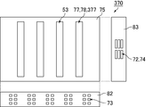
- the openings 377 are formed at substantially the same pitch as the pitch of the injection ports 61 in the X-axis direction, and each opening 377 faces the corresponding openings 77 and 78. That is, when viewed along the Z-axis direction, at least a part of each opening 377 overlaps at least a part of the corresponding opening 77 and also overlaps at least a part of the corresponding opening 78.
Landscapes
- Chemical & Material Sciences (AREA)
- Engineering & Computer Science (AREA)
- Chemical Kinetics & Catalysis (AREA)
- Materials Engineering (AREA)
- Mechanical Engineering (AREA)
- Metallurgy (AREA)
- Organic Chemistry (AREA)
- Manufacturing & Machinery (AREA)
- General Chemical & Material Sciences (AREA)
- Electroluminescent Light Sources (AREA)
- Physical Vapour Deposition (AREA)
Abstract
Description
前記蒸着装置は、蒸着源、制限部材及びマスクを含む蒸着ユニットと、
前記基板を前記マスクから離間させた状態で、前記基板の法線方向に直交する第一方向に沿って、前記基板及び前記蒸着ユニットの一方を他方に対して相対的に移動させる移動機構とを備えてもよく、
前記蒸着源、前記制限部材、前記マスク及び前記基板は、この順に配置されてもよく、
前記制限部材は、第一板部と、
前記第一板部との間に間隔を空けて設けられた第二板部と、
前記第一板部を前記第二板部に接続する接続部とを含んでもよく、
前記第一板部には、開口が設けられてもよく、
前記第二板部には、前記第一板部の前記開口に対向する開口が設けられてもよく、
前記第一板部の前記開口及び前記第二板部の前記開口の間には、第一空間が存在してもよく、
前記基板の前記法線方向及び前記第一方向に直交する第二方向において前記第一空間の隣には、前記第一板部及び前記第二板部の間に第二空間が存在してもよく、
前記第一空間は、前記第二空間とつながってもよく、
前記第一方向において前記第二空間の隣には、前記制限部材の外に第三空間が存在してもよく、
前記第二空間は、前記第三空間とつながってもよい。
以下、この蒸着装置を本発明に係る蒸着装置とも言う。
前記第一壁部は、前記第一空間及び前記第二空間の間に設けられてもよく、
前記第二壁部は、前記第二空間及び前記第三空間の間に設けられてもよく、
前記第一空間は、前記第一壁部の前記開口で前記第二空間とつながってもよく、
前記第二空間は、前記第二壁部の前記開口で前記第三空間とつながってもよい。
前記第二壁部の前記開口は、複数設けられてもよい。
前記第二板部の前記第二開口は、前記第一板部の前記開口以外の領域において前記第一板部に対向してもよい。
前記第一板部の前記第二開口は、前記第二板部の前記開口以外の領域において前記第二板部に対向してもよく、
本発明に係る蒸着装置は、前記第一板部及び前記マスクの間に、前記第一板部との間に間隔を空けて設けられた板材を更に備えてもよく、
前記板材は、前記第一板部の前記第二開口よりも大きくてもよく、また、前記基板の前記法線方向に沿って見たときに前記第二開口の全部に重なってもよい。
前記蒸着工程は、本発明に係る蒸着装置を用いて行われてもよい。
本実施形態では、TFT基板側から光を取り出すボトムエミッション型でRGBフルカラー表示の有機EL素子の製造方法と、その製造方法により作製された有機EL素子を備える有機EL表示装置とについて主に説明するが、本実施形態は、他のタイプの有機EL素子の製造方法にも適用可能である。
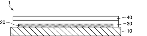
図1は、実施形態1の有機EL素子の製造方法により作製された有機EL素子を備える有機EL表示装置の断面模式図である。図2は、図1に示した有機EL表示装置の表示領域内の構成を示す平面模式図である。図3は、図1に示した有機EL表示装置のTFT基板の構成を示す断面模式図であり、図2中のA-B線における断面に相当する。
(1)第1電極/発光層/第2電極
(2)第1電極/正孔輸送層/発光層/電子輸送層/第2電極
(3)第1電極/正孔輸送層/発光層/正孔ブロッキング層/電子輸送層/第2電極
(4)第1電極/正孔輸送層/発光層/正孔ブロッキング層/電子輸送層/電子注入層/第2電極
(5)第1電極/正孔注入層/正孔輸送層/発光層/電子輸送層/電子注入層/第2電極
(6)第1電極/正孔注入層/正孔輸送層/発光層/正孔ブロッキング層/電子輸送層/第2電極
(7)第1電極/正孔注入層/正孔輸送層/発光層/正孔ブロッキング層/電子輸送層/電子注入層/第2電極
(8)第1電極/正孔注入層/正孔輸送層/電子ブロッキング層(キャリアブロッキング層)/発光層/正孔ブロッキング層/電子輸送層/電子注入層/第2電極
なお、上述のように、正孔注入層と正孔輸送層とは、一体化されていてもよい。また、電子輸送層と電子注入層とは、一体化されていてもよい。
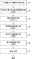
図4は、実施形態1の有機EL表示装置の製造工程を説明するためのフローチャートである。
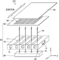
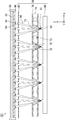
図5は、実施形態1の蒸着装置の斜視模式図である。図6は、実施形態1の蒸着装置の断面模式図であり、基板の走査方向に垂直な断面を示す。
以下、制限部材70について詳述する。
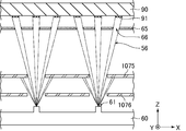
図12に示すように、本比較形態は、制限部材70の代わりに、二種類の制限板1075及び1076を別々に配置したことを除いて、実施形態1と実質的に同じである。本比較形態では、制限板1075及び1076に、設置及び交換時のアライメント精度がそれぞれ要求される。そのため、制限板1075及び1076を長期に渡って繰り返し使用する場合、図13に示すように、制限板1075及び/又は1076が所定の位置からずれて配置される可能性が高くなる。制限板1075及び/又は1076のアライメントのズレが発生すると、蒸着流56の向きが変化し、意図しない場所に蒸着粒子が飛来することとなり、均一な薄膜を形成することができなくなる。
本実施形態は、制限部材が異なることを除いて、実施形態1と実質的に同じである。したがって、本実施形態では、本実施形態に特有の特徴について主に説明し、実施形態1と重複する内容については説明を省略する。また、本実施形態と実施形態1とにおいて、同一又は同様の機能を有する部材には同一の符号を付し、本実施形態において、その部材の説明は省略する。
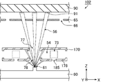
図14及び15に示すように、本実施形態に係る蒸着装置102は、制限部材70の代わりに制限部材170を備えている。制限部材170は、第二板部76の代わりに第二板部176を含んでいることを除いて、制限部材70と実質的に同じであり、第二板部176は、複数の開口78に加えて、第一板部75の下方において複数の第二開口185が形成されていることを除いて、第二板部76と実質的に同じである。
本実施形態は、制限部材が異なることと、制限部材の上方に板材を更に備えることとを除いて、実施形態1と実質的に同じである。したがって、本実施形態では、本実施形態に特有の特徴について主に説明し、実施形態1と重複する内容については説明を省略する。また、本実施形態と実施形態1とにおいて、同一又は同様の機能を有する部材には同一の符号を付し、本実施形態において、その部材の説明は省略する。
図16~18に示すように、本実施形態に係る蒸着装置103は、制限部材70の代わりに制限部材270を備えている。制限部材270は、第一板部75の代わりに第一板部275を含んでいることを除いて、制限部材70と実質的に同じであり、第一板部275は、複数の開口77に加えて、第二板部76の上方に複数の第二開口286が形成されていることを除いて、第一板部75と実質的に同じである。
本実施形態は、制限部材が異なることを除いて、実施形態1と実質的に同じである。したがって、本実施形態では、本実施形態に特有の特徴について主に説明し、実施形態1と重複する内容については説明を省略する。また、本実施形態と実施形態1とにおいて、同一又は同様の機能を有する部材には同一の符号を付し、本実施形態において、その部材の説明は省略する。
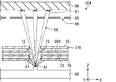
図19及び20に示すように、本実施形態に係る蒸着装置104は、制限部材70の代わりに制限部材370を備えている。
本実施形態は、制限部材が異なることを除いて、実施形態1と実質的に同じである。したがって、本実施形態では、本実施形態に特有の特徴について主に説明し、実施形態1と重複する内容については説明を省略する。また、本実施形態と実施形態1とにおいて、同一又は同様の機能を有する部材には同一の符号を付し、本実施形態において、その部材の説明は省略する。
図21及び22に示すように、本実施形態に係る蒸着装置は、制限部材70の代わりに制限部材470を備えている。制限部材470は、接続部として、第一、第二、第三及び第四壁部81、82、83及び84の代わりに、複数の第五壁部489を含んでいることを除いて、制限部材70と実質的に同じである。
本実施形態は、制限部材が異なることを除いて、実施形態1と実質的に同じである。したがって、本実施形態では、本実施形態に特有の特徴について主に説明し、実施形態1と重複する内容については説明を省略する。また、本実施形態と実施形態1とにおいて、同一又は同様の機能を有する部材には同一の符号を付し、本実施形態において、その部材の説明は省略する。
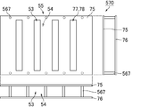
図23及び24に示すように、本実施形態に係る蒸着装置は、制限部材70の代わりに制限部材570を備えている。制限部材570は、接続部として、第一、第二、第三及び第四壁部81、82、83及び84の代わりに、複数の柱部567を含んでいることを除いて、制限部材70と実質的に同じである。
実施形態1~6で説明した平板状の部材は、平板以外の形状であってもよく、例えば、屈曲及び/又は湾曲していてもよく、波板状であってもよい。
本比較形態は、制限部材の代わりに制限板を備えることを除いて、実施形態1と実質的に同じである。したがって、本比較形態では、本実施形態に特有の特徴について主に説明し、実施形態1と重複する内容については説明を省略する。また、本比較形態と実施形態1とにおいて、同一又は同様の機能を有する部材には同一の符号を付し、本比較形態において、その部材の説明は省略する。
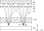
図25に示すように、本比較形態に係る蒸着装置は、制限部材70の代わりに制限板1170を備えている。制限板1170は、1枚の厚板から形成された部材であり、射出口61に対応して複数の開口1177が設けられている。
2:画素
2R、2G、2B:サブ画素
10:TFT基板
11:絶縁基板
12:TFT
13:層間膜
13a:コンタクトホール
14:配線
15:エッジカバー
15R、15G、15B:開口部
20:有機EL素子
21:第1電極
22:正孔注入層兼正孔輸送層(有機層)
23R、23G、23B:発光層(有機層)
24:電子輸送層(有機層)
25:電子注入層(有機層)
26:第2電極
30:接着層
40:封止基板
50:蒸着ユニット
51:保持機構(保持装置)
52:移動機構(移動装置)
53:第一空間
54:第二空間
55:第三空間
56:蒸着流
60:蒸着源
61:射出口
62:ノズル
65:マスク(蒸着マスク)
70、170、270、370、470、570:制限部材
71:貫通口
66、72、73、74、77、78、377:開口
75、275:第一板部
76、176:第二板部
80:接続部
81:第一壁部
82:第二壁部
83:第三壁部
84:第四壁部
90:基板(被成膜基板)
91:薄膜のパターン
101、102、103、104:蒸着装置
185、286:第二開口
268:接続部
287:板材
388:第三板部
489:第五壁部
567:柱部
Claims (8)
- 基板上に薄膜のパターンを形成する蒸着装置であって、
前記蒸着装置は、蒸着源、制限部材及びマスクを含む蒸着ユニットと、
前記基板を前記マスクから離間させた状態で、前記基板の法線方向に直交する第一方向に沿って、前記基板及び前記蒸着ユニットの一方を他方に対して相対的に移動させる移動機構とを備え、
前記蒸着源、前記制限部材、前記マスク及び前記基板は、この順に配置され、
前記制限部材は、第一板部と、
前記第一板部との間に間隔を空けて設けられた第二板部と、
前記第一板部を前記第二板部に接続する接続部とを含み、
前記第一板部には、開口が設けられ、
前記第二板部には、前記第一板部の前記開口に対向する開口が設けられ、
前記第一板部の前記開口及び前記第二板部の前記開口の間には、第一空間が存在し、
前記基板の前記法線方向及び前記第一方向に直交する第二方向において前記第一空間の隣には、前記第一板部及び前記第二板部の間に第二空間が存在し、
前記第一空間は、前記第二空間とつながり、
前記第一方向において前記第二空間の隣には、前記制限部材の外に第三空間が存在し、
前記第二空間は、前記第三空間とつながる蒸着装置。 - 前記制限部材は、前記接続部として、開口が各々設けられた第一壁部及び第二壁部を含み、
前記第一壁部は、前記第一空間及び前記第二空間の間に設けられ、
前記第二壁部は、前記第二空間及び前記第三空間の間に設けられ、
前記第一空間は、前記第一壁部の前記開口で前記第二空間とつながり、
前記第二空間は、前記第二壁部の前記開口で前記第三空間とつながる請求項1記載の蒸着装置。 - 前記第一壁部の前記開口は、複数設けられ、
前記第二壁部の前記開口は、複数設けられる請求項2記載の蒸着装置。 - 前記第二板部には、第二開口が設けられ、
前記第二板部の前記第二開口は、前記第一板部の前記開口以外の領域において前記第一板部に対向する請求項1~3のいずれかに記載の蒸着装置。 - 前記第一板部には、第二開口が設けられ、
前記第一板部の前記第二開口は、前記第二板部の前記開口以外の領域において前記第二板部に対向し、
前記蒸着装置は、前記第一板部及び前記マスクの間に、前記第一板部との間に間隔を空けて設けられた板材を更に備え、
前記板材は、前記第一板部の前記第二開口よりも大きく、かつ、前記基板の前記法線方向に沿って見たときに前記第二開口の全部に重なる請求項1~4のいずれかに記載の蒸着装置。 - 前記制限部材は、前記板材を前記第一板部に接続する接続部を更に含む請求項5記載の蒸着装置。
- 基板上に薄膜のパターンを形成する蒸着工程を含む蒸着方法であって、
前記蒸着工程は、請求項1~6のいずれかに記載の蒸着装置を用いて行われる蒸着方法。 - 請求項1~6のいずれかに記載の蒸着装置を用いて薄膜のパターンを形成する蒸着工程を含む有機エレクトロルミネッセンス素子の製造方法。
Priority Applications (4)
| Application Number | Priority Date | Filing Date | Title |
|---|---|---|---|
| JP2015526181A JP6042988B2 (ja) | 2013-07-08 | 2014-03-04 | 蒸着装置、蒸着方法、及び、有機エレクトロルミネッセンス素子の製造方法 |
| US14/903,603 US9614155B2 (en) | 2013-07-08 | 2014-03-04 | Vapor deposition apparatus, vapor deposition method, and method for producing organic electroluminescent element |
| CN201480039163.9A CN105378139B (zh) | 2013-07-08 | 2014-03-04 | 蒸镀装置、蒸镀方法和有机电致发光元件的制造方法 |
| KR1020167003136A KR101765018B1 (ko) | 2013-07-08 | 2014-03-04 | 증착 장치, 증착 방법 및 유기 일렉트로 루미네센스 소자의 제조 방법 |
Applications Claiming Priority (2)
| Application Number | Priority Date | Filing Date | Title |
|---|---|---|---|
| JP2013142888 | 2013-07-08 | ||
| JP2013-142888 | 2013-07-08 |
Publications (1)
| Publication Number | Publication Date |
|---|---|
| WO2015004945A1 true WO2015004945A1 (ja) | 2015-01-15 |
Family
ID=52279644
Family Applications (1)
| Application Number | Title | Priority Date | Filing Date |
|---|---|---|---|
| PCT/JP2014/055407 Ceased WO2015004945A1 (ja) | 2013-07-08 | 2014-03-04 | 蒸着装置、蒸着方法、及び、有機エレクトロルミネッセンス素子の製造方法 |
Country Status (6)
| Country | Link |
|---|---|
| US (1) | US9614155B2 (ja) |
| JP (1) | JP6042988B2 (ja) |
| KR (1) | KR101765018B1 (ja) |
| CN (1) | CN105378139B (ja) |
| TW (1) | TWI621727B (ja) |
| WO (1) | WO2015004945A1 (ja) |
Cited By (1)
| Publication number | Priority date | Publication date | Assignee | Title |
|---|---|---|---|---|
| WO2017069036A1 (ja) * | 2015-10-20 | 2017-04-27 | シャープ株式会社 | 制限ユニット、蒸着装置、蒸着膜製造方法、エレクトロルミネッセンス表示装置の生産方法およびエレクトロルミネッセンス表示装置 |
Families Citing this family (5)
| Publication number | Priority date | Publication date | Assignee | Title |
|---|---|---|---|---|
| KR102437101B1 (ko) * | 2015-12-24 | 2022-08-29 | 삼성디스플레이 주식회사 | 유기층 증착 어셈블리, 이를 포함하는 유기층 증착 장치 및 이를 이용한 유기 발광 표시 장치의 제조 방법 |
| TWI721170B (zh) | 2016-05-24 | 2021-03-11 | 美商伊麥傑公司 | 蔽蔭遮罩沉積系統及其方法 |
| CN109642313B (zh) * | 2016-05-24 | 2021-03-09 | 埃马金公司 | 高精准度蔽荫掩模沉积系统及其方法 |
| US12201037B2 (en) * | 2019-11-06 | 2025-01-14 | International Business Machines Corporation | Cluster tool for production-worthy fabrication of Dolan bridge quantum Josephson junction devices |
| EP4162094A4 (en) * | 2020-06-04 | 2024-10-02 | Applied Materials, Inc. | Vapor deposition apparatus and method for coating a substrate in a vacuum chamber |
Citations (4)
| Publication number | Priority date | Publication date | Assignee | Title |
|---|---|---|---|---|
| US20050183670A1 (en) * | 2002-09-24 | 2005-08-25 | Grantham Daniel H. | Patterned thin-film deposition using collimating heated masked assembly |
| WO2011148750A1 (ja) * | 2010-05-28 | 2011-12-01 | シャープ株式会社 | 蒸着マスク及びこれを用いた有機el素子の製造方法と製造装置 |
| WO2012029545A1 (ja) * | 2010-08-30 | 2012-03-08 | シャープ株式会社 | 蒸着方法、蒸着装置、及び有機el表示装置 |
| WO2012086453A1 (ja) * | 2010-12-21 | 2012-06-28 | シャープ株式会社 | 蒸着装置、蒸着方法、及び有機el表示装置 |
Family Cites Families (6)
| Publication number | Priority date | Publication date | Assignee | Title |
|---|---|---|---|---|
| TWI252706B (en) * | 2002-09-05 | 2006-04-01 | Sanyo Electric Co | Manufacturing method of organic electroluminescent display device |
| JP5620146B2 (ja) | 2009-05-22 | 2014-11-05 | 三星ディスプレイ株式會社Samsung Display Co.,Ltd. | 薄膜蒸着装置 |
| JP5502092B2 (ja) | 2009-09-15 | 2014-05-28 | シャープ株式会社 | 蒸着方法および蒸着装置 |
| KR101483354B1 (ko) | 2010-05-18 | 2015-01-15 | 샤프 가부시키가이샤 | 유기 el 소자의 제조 방법 및 제조 장치 |
| CN103282543B (zh) | 2011-03-10 | 2014-12-24 | 夏普株式会社 | 蒸镀装置和蒸镀方法 |
| JP6363333B2 (ja) * | 2013-08-07 | 2018-07-25 | シャープ株式会社 | 蒸着装置、及び、有機エレクトロルミネッセンス素子の製造方法 |
-
2014
- 2014-03-04 KR KR1020167003136A patent/KR101765018B1/ko not_active Expired - Fee Related
- 2014-03-04 CN CN201480039163.9A patent/CN105378139B/zh not_active Expired - Fee Related
- 2014-03-04 JP JP2015526181A patent/JP6042988B2/ja not_active Expired - Fee Related
- 2014-03-04 WO PCT/JP2014/055407 patent/WO2015004945A1/ja not_active Ceased
- 2014-03-04 US US14/903,603 patent/US9614155B2/en not_active Expired - Fee Related
- 2014-04-03 TW TW103112612A patent/TWI621727B/zh not_active IP Right Cessation
Patent Citations (4)
| Publication number | Priority date | Publication date | Assignee | Title |
|---|---|---|---|---|
| US20050183670A1 (en) * | 2002-09-24 | 2005-08-25 | Grantham Daniel H. | Patterned thin-film deposition using collimating heated masked assembly |
| WO2011148750A1 (ja) * | 2010-05-28 | 2011-12-01 | シャープ株式会社 | 蒸着マスク及びこれを用いた有機el素子の製造方法と製造装置 |
| WO2012029545A1 (ja) * | 2010-08-30 | 2012-03-08 | シャープ株式会社 | 蒸着方法、蒸着装置、及び有機el表示装置 |
| WO2012086453A1 (ja) * | 2010-12-21 | 2012-06-28 | シャープ株式会社 | 蒸着装置、蒸着方法、及び有機el表示装置 |
Cited By (1)
| Publication number | Priority date | Publication date | Assignee | Title |
|---|---|---|---|---|
| WO2017069036A1 (ja) * | 2015-10-20 | 2017-04-27 | シャープ株式会社 | 制限ユニット、蒸着装置、蒸着膜製造方法、エレクトロルミネッセンス表示装置の生産方法およびエレクトロルミネッセンス表示装置 |
Also Published As
| Publication number | Publication date |
|---|---|
| KR101765018B1 (ko) | 2017-08-03 |
| TWI621727B (zh) | 2018-04-21 |
| KR20160027197A (ko) | 2016-03-09 |
| CN105378139A (zh) | 2016-03-02 |
| US9614155B2 (en) | 2017-04-04 |
| TW201502301A (zh) | 2015-01-16 |
| US20160155944A1 (en) | 2016-06-02 |
| CN105378139B (zh) | 2017-06-13 |
| JP6042988B2 (ja) | 2016-12-14 |
| JPWO2015004945A1 (ja) | 2017-03-02 |
Similar Documents
| Publication | Publication Date | Title |
|---|---|---|
| JP5766239B2 (ja) | 蒸着装置及び蒸着方法 | |
| CN103124803B (zh) | 蒸镀方法、蒸镀装置和有机el显示装置 | |
| US9231210B2 (en) | Manufacturing device and manufacturing method for organic EL element | |
| JP5612106B2 (ja) | 蒸着方法、蒸着装置、及び有機el表示装置 | |
| JP5259886B2 (ja) | 蒸着方法及び蒸着装置 | |
| JP5350547B2 (ja) | 被成膜基板および有機el表示装置 | |
| JP6199967B2 (ja) | 有機エレクトロルミネッセンス素子の製造方法 | |
| JP6087267B2 (ja) | 蒸着装置、蒸着方法、及び、有機エレクトロルミネッセンス素子の製造方法 | |
| JP6429491B2 (ja) | 蒸着装置用マスク、蒸着装置、蒸着方法、及び、有機エレクトロルミネッセンス素子の製造方法 | |
| WO2012086453A1 (ja) | 蒸着装置、蒸着方法、及び有機el表示装置 | |
| JPWO2012099019A1 (ja) | 有機el表示装置および蒸着方法 | |
| JP6042988B2 (ja) | 蒸着装置、蒸着方法、及び、有機エレクトロルミネッセンス素子の製造方法 | |
| CN103340012B (zh) | 被成膜基板、有机el显示装置 |
Legal Events
| Date | Code | Title | Description |
|---|---|---|---|
| 121 | Ep: the epo has been informed by wipo that ep was designated in this application |
Ref document number: 14823576 Country of ref document: EP Kind code of ref document: A1 |
|
| ENP | Entry into the national phase |
Ref document number: 2015526181 Country of ref document: JP Kind code of ref document: A |
|
| NENP | Non-entry into the national phase |
Ref country code: DE |
|
| WWE | Wipo information: entry into national phase |
Ref document number: 14903603 Country of ref document: US |
|
| ENP | Entry into the national phase |
Ref document number: 20167003136 Country of ref document: KR Kind code of ref document: A |
|
| 122 | Ep: pct application non-entry in european phase |
Ref document number: 14823576 Country of ref document: EP Kind code of ref document: A1 |