WO2014203552A1 - 電力変換装置 - Google Patents
電力変換装置 Download PDFInfo
- Publication number
- WO2014203552A1 WO2014203552A1 PCT/JP2014/051886 JP2014051886W WO2014203552A1 WO 2014203552 A1 WO2014203552 A1 WO 2014203552A1 JP 2014051886 W JP2014051886 W JP 2014051886W WO 2014203552 A1 WO2014203552 A1 WO 2014203552A1
- Authority
- WO
- WIPO (PCT)
- Prior art keywords
- power
- case
- power semiconductor
- conversion device
- opening
- Prior art date
Links
Images


Classifications
-
- H—ELECTRICITY
- H02—GENERATION; CONVERSION OR DISTRIBUTION OF ELECTRIC POWER
- H02M—APPARATUS FOR CONVERSION BETWEEN AC AND AC, BETWEEN AC AND DC, OR BETWEEN DC AND DC, AND FOR USE WITH MAINS OR SIMILAR POWER SUPPLY SYSTEMS; CONVERSION OF DC OR AC INPUT POWER INTO SURGE OUTPUT POWER; CONTROL OR REGULATION THEREOF
- H02M7/00—Conversion of ac power input into dc power output; Conversion of dc power input into ac power output
- H02M7/003—Constructional details, e.g. physical layout, assembly, wiring or busbar connections
-
- H—ELECTRICITY
- H05—ELECTRIC TECHNIQUES NOT OTHERWISE PROVIDED FOR
- H05K—PRINTED CIRCUITS; CASINGS OR CONSTRUCTIONAL DETAILS OF ELECTRIC APPARATUS; MANUFACTURE OF ASSEMBLAGES OF ELECTRICAL COMPONENTS
- H05K7/00—Constructional details common to different types of electric apparatus
- H05K7/14—Mounting supporting structure in casing or on frame or rack
- H05K7/1422—Printed circuit boards receptacles, e.g. stacked structures, electronic circuit modules or box like frames
- H05K7/1427—Housings
- H05K7/1432—Housings specially adapted for power drive units or power converters
- H05K7/14322—Housings specially adapted for power drive units or power converters wherein the control and power circuits of a power converter are arranged within the same casing
-
- H—ELECTRICITY
- H05—ELECTRIC TECHNIQUES NOT OTHERWISE PROVIDED FOR
- H05K—PRINTED CIRCUITS; CASINGS OR CONSTRUCTIONAL DETAILS OF ELECTRIC APPARATUS; MANUFACTURE OF ASSEMBLAGES OF ELECTRICAL COMPONENTS
- H05K7/00—Constructional details common to different types of electric apparatus
- H05K7/20—Modifications to facilitate cooling, ventilating, or heating
- H05K7/2089—Modifications to facilitate cooling, ventilating, or heating for power electronics, e.g. for inverters for controlling motor
- H05K7/209—Heat transfer by conduction from internal heat source to heat radiating structure
-
- H—ELECTRICITY
- H02—GENERATION; CONVERSION OR DISTRIBUTION OF ELECTRIC POWER
- H02M—APPARATUS FOR CONVERSION BETWEEN AC AND AC, BETWEEN AC AND DC, OR BETWEEN DC AND DC, AND FOR USE WITH MAINS OR SIMILAR POWER SUPPLY SYSTEMS; CONVERSION OF DC OR AC INPUT POWER INTO SURGE OUTPUT POWER; CONTROL OR REGULATION THEREOF
- H02M1/00—Details of apparatus for conversion
- H02M1/32—Means for protecting converters other than automatic disconnection
- H02M1/327—Means for protecting converters other than automatic disconnection against abnormal temperatures
Definitions
- the present invention relates to a power conversion device.
- Inverters which are power conversion devices, are widely used as speed control devices for AC motors in industry and home appliances.
- IPM integer power modules
- Patent Document 1 “as a result of placing the lid portion 20c on the substrate 50, the plurality of lead frames 23 and the plurality of metal foils 12 on the substrate 50 come into contact with each other. The parts are soldered to electrically connect each lead frame 23 and each metal foil 12. Also, the lead frame 23 and each metal foil 12 are joined, so that the lid 20c. Is fixed on the substrate 50 ".
- FIG. 20 discloses an opening that penetrates the lead frame (lead terminal), an empty opening that does not penetrate the lead frame, and an opening for gel injection.
- Line 20 says, “Compared to the conventional M711 package with the same rated current, the compact flexible PIM has reduced the mounting area by 45% and the mass by 75% ⁇ ⁇ . This reduces the size and cost of customer equipment. It can make a big contribution. ”
- Patent Document 1 and Non-Patent Document 1 describe an opening that penetrates the lead frame (lead terminal) and an empty opening that does not penetrate the lead frame on the upper surface of the power semiconductor module.
- the degree of freedom in manufacturing the power semiconductor module can be increased.
- the lead frame can be provided at any location
- the surrounding air is supplied to the inside of the module through the empty opening through which the lead frame does not penetrate and the opening for gel injection, when the power semiconductor breaks down, it easily combines with the surrounding air and ignites. easy.
- the conventional power semiconductor module is composed of a hard resin and a lid, when the power semiconductor breaks down, it has a structure that is not easily combined with the surrounding air.
- a power semiconductor a cooling fin that cools the power semiconductor, a first case that is disposed between the power semiconductor and the cooling fin and includes an opening that matches the shape of the power semiconductor, and the power semiconductor. And a second case for covering the lead terminal opening.
- a flame due to abnormal heat generated inside is ejected from an empty opening or a gel injection opening that does not penetrate the lead frame, and the other inside the power converter. Secondary fire spread due to the spread of fire to parts and the like can be prevented.
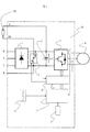
- Example 1 is an example of a configuration diagram of a power converter according to the present invention.
- FIG. 1 shows a case where an AC power source is used as an arbitrary input power source.
- Forward converter unit 1 converts AC power into DC power.
- the smoothing capacitor 2 is provided on the output side of the forward converter unit 1.
- the reverse converter unit 3 converts DC power into AC power having an arbitrary frequency.
- an IGBT is mounted in the inverse converter unit 3 as a typical switching element.
- the switching element is not limited to the IGBT, and any element having a form as a switching element may be used.
- the cooling fan 6 cools the power semiconductor modules in the forward converter unit 1, the regenerative braking unit 9, and the reverse converter unit 3.
- the digital operation panel 7 sets, changes, abnormal states, and monitor displays various control data of the power conversion device.
- the operation panel 7 is provided with a display unit capable of displaying an abnormality. When an abnormality is detected in the power conversion device, the display is displayed on the display unit.
- the type of the operation panel 7 of the present embodiment is not particularly limited. However, the operation panel 7 is configured as a digital operation panel so that the operation can be performed while viewing the display on the display unit in consideration of the operability of the apparatus user. .
- the display unit is not necessarily configured integrally with the operation panel 7, but it is desirable that the display unit be configured integrally so that an operator of the operation panel 7 can operate while viewing the display.
- Various control data of the power converter input from the operation panel 7 is stored in a storage unit (not shown).
- the control circuit 5 controls the switching elements in the reverse converter unit 3 and the regenerative braking unit 9 based on various control data input from the digital operation panel 7, and also has a function of controlling the power converter 10 as a whole. Therefore, a microcomputer (control arithmetic unit) is mounted and is configured to perform necessary control processing according to various control data input from the digital operation panel 7.
- a microcomputer control arithmetic unit that performs an operation based on information from storage data of a storage unit that stores various control data is mounted.
- the current detector CT detects the U-phase and W-phase line currents of the AC motor.
- FIG. 1 shows an example in which two CTs are used, but three CTs may be used to detect line currents of each U phase, V phase, and W phase.
- the drive circuit 8 drives the switching elements in the inverse converter unit 3 and the regenerative braking unit 9 based on a command from the control circuit 5.
- a switching regulator circuit (DC / DC converter) is mounted in the drive circuit 8, and each DC voltage necessary for the operation of the power converter is generated and supplied to each component.
- the regenerative braking resistor BR plays a role of consuming rotational energy during deceleration of the AC motor as heat energy to the resistor.
- the DC power supply + side is connected to the DC terminal P side, and the DC power supply -side is connected to the DC terminal N side.
- the AC terminals R, S, and T may be connected, the DC power supply + side may be connected to this connection point, and the DC power supply N side may be connected to the DC power supply negative side.
- the positive side of the DC power source may be connected to the P side, the AC terminals R, S, and T may be connected, and the negative side of the DC power source may be connected to this connection point.
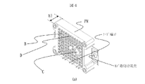
- FIG. 2 is an example of a bird's-eye view of the power conversion device according to the present invention.
- Example 2 of the power converter device by this invention is demonstrated using a figure below.
- the power semiconductor PM is a module including a forward converter unit 1, an inverse converter unit 3, and a regenerative braking unit 9. A state where a case 15 is attached to the power semiconductor is shown.
- the power semiconductor PM is fixed to the cooling fin by screws (not shown).
- a lead terminal of the power semiconductor is passed through a through hole provided in the substrate PCB on which the drive circuit 8 is mounted, and is electrically connected by solder (solder).
- the substrate on which the control circuit 5 is mounted and the substrate PCB on which the drive circuit 8 is mounted are connected by an electric wire.
- the cooling fin 11 conducts heat from the power semiconductor, which is a heating element, sends air to the cooling fin by a cooling fan (not shown), and performs heat exchange to dissipate heat by an air cooling method.
- the positioning case 16 is provided with an opening in advance according to the power semiconductor so that the mounting position of the power semiconductor can be easily determined when the power semiconductor PM is mounted on the cooling fin, and the mounting position of the power semiconductor is fixed.
- the module composed of the forward converter unit 1, the reverse converter unit 3, and the regenerative braking unit 9 is taken as an example.
- the power semiconductor and the reverse converter unit 3 composed of only the forward converter unit 1 are used. Even if two power semiconductors composed of the regenerative braking unit 9 are used, the forward converter unit 1, the reverse converter unit 3, and the regenerative braking unit 9 are used individually for the three power semiconductors.
- the intention of the invention remains the same.
- the casing of the power conversion device includes a cooling fin 11, a casing 12, a wire drawing plate 13, and a surface cover 14.
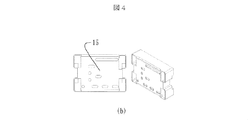
- FIG. 3 is a bird's-eye view (first form) of the positioning case 16 of the power conversion device according to the present invention.
- (A) is a bird's eye view in which protrusions (barriers) 17 are provided on the four sides of the opening A provided in the positioning case 16 according to the power semiconductor PM.
- (B) is a bird's-eye view in which protrusions (barriers) 17 are provided on two sides of the opening A provided in the positioning case 16.
- (C) is a bird's eye view in which no protrusion (barrier) is provided in the opening A provided in the positioning case 16.
- the height h1 of the protrusion 17 is designed to be lower than the height h2 (see FIG. 4A) of the power semiconductor PM.
- the projections 17 are provided on the four sides and two sides of the opening A, but not provided, but the number of sides on which the projections are provided is not limited.
- (D) is a front view and a bird's-eye view of a state in which the power semiconductor covered with the positioning case 16 and the case 15 described in (c) is mounted on a cooling fin.
- (E) is a front view and a bird's-eye view of a state in which the power semiconductor covered with the positioning case and the case 15 described in (a) is mounted on a cooling fin.
- the projections 17 on the four sides provided in the positioning case 16 hold the case 15 covered with the power semiconductor PM, and the power is prevented so that flames due to abnormal heat generation are not ejected due to an increase in internal pressure inside the module when the power semiconductor is broken. It can be seen that the gap with the semiconductor can be reduced.
- the gaps on the four sides can be made smaller than in the case (c) in which no protrusions are provided on the opening A. The effect of suppressing the force that comes out is great.
- FIG. 4 is a bird's-eye view (second embodiment) of the case 15 of the power conversion device according to the present invention.
- Example 2 of the power converter device by this invention is demonstrated using a figure below.
- (A) is an example of a bird's-eye view of the power semiconductor PM, and has 69 empty openings B and one opening C for gel injection through which lead terminals do not penetrate. Of course, there is also a gap on the contact surface D through which the 20 lead terminals pass.
- the reason for providing a plurality of openings is that when manufacturing custom power semiconductor modules dedicated to customers, if a plurality of openings are provided in advance, the lead frame can be provided at any place, and the custom power semiconductor This is because the module has a manufacturing advantage that a standard power semiconductor module case can be shared.
- (B) is a front view and a bird's-eye view of the case 15 in one embodiment.
- the cover is provided with oval and circular openings in accordance with all the lead terminal positions of the power semiconductor. Of course, it may be a rectangular opening.
- (C) is a front view and a bird's-eye view of the case 15 in another embodiment.
- the difference from the cover described in the embodiment of (b) is to secure an electrical insulation distance from the component mounted on the back surface of the substrate PCB, the lead of the component, and the screw for mounting the power semiconductor to the cooling fin.
- the protrusion part E provided in both ends. Details of this example will be described later.
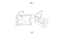
- (D) is a front view and a rear bird's-eye view of the case 15 provided with a protrusion (boss) 18 that closes the opening C for gel injection of the power semiconductor.
- the bird's-eye view shows a state in which the case 15 is viewed from the back so that the protrusion 18 can be identified.
- the protrusion is slightly tapered so that it can be easily inserted into the opening for gel injection, and the tip is thin. Of course, it may be a quadrangular protrusion (boss).
- the length of the protrusion may be designed according to the depth of the power semiconductor gel injection opening.
- (E) is a front view and a bird's-eye view of a case in which protrusions 19 are provided on four sides.
- the protrusions 19 provided on the four sides of the case have contact with the protrusions provided on the four sides on the back surface of the substrate PCB on which the drive circuit 8 is mounted, so that the back surface of the substrate PCB serves as a lid and can eliminate gaps. It is what I did.
- the protrusion 19 is not limited to four sides, and two sides are also effective.
- the method (e) can eliminate the gap more effectively. Details of this example will be described later.
- (F) is a front view and a bird's-eye view of a case in which 20 circular openings F are provided in accordance with the shape and number of lead terminals of the power semiconductor.
- the gap between the lead terminal and the opening of the case can be further reduced with respect to the case of the embodiment in (b) to (e).
- (G) is a bird's-eye view showing a state where the case is attached to the power semiconductor.
- the purpose is to cover the power semiconductor with the case by moving the case in the direction of the arrow and covering the power semiconductor so that the 20 lead terminals of the power semiconductor pass through the opening provided in the case 15.
- This is a feature of the present invention.
- the case thickness t is designed to be 0.71 mm or more.
- the case covers the power semiconductor, and a flame due to abnormal heat generated inside when the semiconductor module is broken is ejected from an empty opening B or an opening C for gel injection that does not penetrate the lead frame. Prevent secondary fire spreading due to fire spreading to other parts inside.
- the case is molded using an insulating resin such as silicon or plastic. Considering ease of handling, the case made of highly flexible silicon is more realistic in terms of workability.
- FIG. 5 is a bird's-eye view (third embodiment) showing the relationship between the substrate PCB and the case 15 of the power conversion device according to the present invention.
- (A) is a bird's-eye view showing a state in which a lead terminal of a power semiconductor is passed through a through hole (not shown) of a substrate PCB on which the drive circuit 8 is mounted and is electrically connected with solder.
- the bird's-eye view is a view seen from the back side of the substrate.
- ⁇ Lead feet of the mounted parts pass through through holes (not shown) on the board and come out from the back side of the board. 20 and 21 are shown as typical lead feet on the back surface.
- the power semiconductor with the case 15 covered on the cooling fin and the positioning case 16 are attached, and the lead terminal of the power semiconductor is inserted into the through hole of the board and soldered. For this reason, when the projections 19 provided on the four sides of the case 15 shown in FIG. 4 (e) are in contact with the back surface of the substrate, the back surface of the substrate PCB serves as a lid, and a gap can be eliminated.
- the component mounting design of the substrate may be made in advance by avoiding the protrusion so that the component is not mounted on the portion where the rear surface of the substrate contacts the protrusion.
- (B) is an enlarged view of a portion surrounded by a dotted line in (a).
- the power semiconductor is attached to a cooling fin (not shown) with a mounting screw.
- a mounting screw This is an example in which the distance d between the head of the screw and the lead foot 20 of the mounting component coming out from the back surface of the board is not equal to or more than a predetermined insulation distance. Electricity provided on the cover 15 covered with the power semiconductor Since the lead foot is surrounded by the protruding portion E for securing the effective insulation distance, the insulation distance can be reduced and the power converter can be downsized.
- FIG. 6 is a diagram (fourth embodiment) in a state where an insulating resin is applied to the opening of the power semiconductor of the power conversion device according to the present invention.
- Embodiments of a power converter according to Embodiment 4 of the present invention will be described below with reference to the drawings.
- Example 1 The difference from Example 1 is that silicon or an insulating resin is applied instead of the molded case 15 to close the opening B or the opening C for gel injection.
- a place where an insulating resin is collectively applied to a part of an opening of a power semiconductor and a place where potting is applied are described as examples. Either one of these methods (batch application or potting application) may be used to apply all the openings (B and C) with an insulating resin, or both (batch application and potting application) may be used together in consideration of workability. It is more realistic to apply all the openings (B and C). Of course, silicon or insulating resin may be applied around the opening D through which the lead frame passes.
- (B) shows an enlarged bird's-eye view of the power semiconductor describing the relationship between the opening and the lead terminal.
- the flame due to abnormal heat generated inside when the semiconductor module is broken is blown out from an empty opening or a gel injection opening that does not penetrate the lead frame. Secondary fire spreading of the power conversion device due to fire spreading to other components inside the power conversion device can be prevented.
Landscapes
- Engineering & Computer Science (AREA)
- Microelectronics & Electronic Packaging (AREA)
- Power Engineering (AREA)
- Physics & Mathematics (AREA)
- Thermal Sciences (AREA)
- Inverter Devices (AREA)
Abstract
半導体モジュールが破壊した際に内部に発生する異常発熱による炎が開口部などから噴き出し、電力変換装置内部の他の部品などへの延焼による電力変換装置の二次的延焼が発生するという可能性があるという問題がある。 パワー半導体と、パワー半導体を冷却する冷却フィンと、前記パワー半導体と前記冷却フィンとの間に配置され、前記パワー半導体の形状に合わせた開口部を備える第一のケースと、前記パワー半導体に設けられたリード端子用の開口部を覆う第二のケースと、を備える電力変換装置である。
Description
本発明は、電力変換装置に関する。
電力変換装置であるインバータは、産業界をはじめ家電製品にも交流電動機の速度制御装置として多く採用されている。
電力変換装置は、IGBTなどのパワー半導体素子(電力用半導体素子)をスイッチング駆動させることにより電圧と周波数の可変制御が行われるが、小型化のため保護回路などの周辺回路を同一のパッケージに組込んだ半導体モジュール、いわゆるIPM(インテリジェント・パワー・モジュール)が用いられている。
一方、高効率化・小型化・低価格化の要求は強く、加工技術の微細化による半導体チップのサイズ縮小(シュリンク)と高性能化により、同一定格の電流に対し従来パッケージより小型のパッケージで対応できるようになってきている。
しかし、半導体モジュール製造上の自由度を上げることが重視され、モジュールの構造上、必ずしもユーザ側の要求にマッチしたものではないことがある。
富士電機技報2012 vol.85 no.6P.426-429
特許文献1の段落[0051]には、「蓋部20cを基板50上に載置した結果、複数のリードフレーム23と、基板50上の複数の金属箔12とが接触する。そして、接触した部分の半田付けを行い、それぞれのリードフレーム23と、それぞれの金属箔12とを電気的に接続する。また、リードフレーム23と、それぞれの金属箔12とを接合させたことにより、蓋部20cが基板50上に固定される。」と記載されている。
また、非特許文献1の第426頁左欄第21行から第24行には、「新しい小容量IGBTモジュールとしてブレーキ付きインバータ・コンバータ用モジュール“小型フレキシブルPIM(Power Integrated Module)”を開発し、系列化した。」ことが、また、第426頁左欄第27行から右上欄第2行には、「構造面では、従来のIGBT モジュール製品とは異なり、銅ベースを使用しないことにより大幅な小型化・軽量化を実現した。」点が記載されている。
さらに、第427頁の左上には、図1に半導体モジュールとして小型フレキシブルPIMの外観写真が掲載されている。写真には、リードフレーム(リード端子)を貫通する開口部、リードフレームが貫通していない空きの開口部、ゲル注入用の開口部が開示されており、第426頁右欄第18行から第20行には、「従来品で同じ定格電流のM711パッケージと比較すると、小型フレキシブルPIMは,取付け面積で45%、質量で75% 削減した。これにより、顧客装置の小型化・低コスト化に大きく貢献できる。」点が記載されている。
特許文献1および非特許文献1には、パワー半導体モジュールの上面にリードフレーム(リード端子)を貫通する開口部とリードフレームが貫通していない空きの開口部が記載されている。複数の開口部を設けることにより、パワー半導体モジュール製造上の自由度を上げることができる。パワー半導体内部の半導体チップの実装位置や他に半導体チップを追加するなど顧客専用のカスタムパワー半導体モジュールを製造する場合において、予め複数の開口部を設けておけば、リードフレームを自由な箇所に設けることができ、カスタムパワー半導体モジュールに対しても、標準のパワー半導体モジュールケースを共用できるという製造上の利点がある。
しかし、リードフレームが貫通していない空きの開口部やゲル注入用の開口部を通して周りの空気がモジュール内部に供給されるため、パワー半導体が破壊した場合、周りの空気と容易に結合し発火し易い。
従来のパワー半導体モジュールは、ハードレジンや蓋で構成されているためパワー半導体が破壊した場合、周りの空気と容易に結合しにくい構造になっている。
すなわち、パワー半導体が破壊した際のモジュール内部の内圧上昇により、異常発熱に起因した炎が開口部などから噴き出し、空気と結合して電力変換装置内部の他の部品などへ延焼し電力変換装置の二次的延焼を誘発する可能性があるという問題がある。
上記目的と達成する手段は下記の通りである。
パワー半導体と、パワー半導体を冷却する冷却フィンと、前記パワー半導体と前記冷却フィンとの間に配置され、前記パワー半導体の形状に合わせた開口部を備える第一のケースと、前記パワー半導体に設けられたリード端子用の開口部を覆う第二のケースと、を備える電力変換装置である。
本発明によれば、パワー半導体が破壊した際に内部に発生する異常発熱による炎がリードフレームを貫通していない空きの開口部やゲル注入用開口部などから噴出し、電力変換装置内部の他の部品などへの延焼による二次的延焼を防止することができる。
以下図面を用いて本発明について説明する。なお、各図における共通の構成については同一の参照番号を付してある。また、本発明は図示例に限定されるものではない。
本発明による電力変換装置の実施例1における形態を以下に図を用いて説明する。
図1は、本発明に係る電力変換装置の構成図の一例である。
図1は、本発明に係る電力変換装置の構成図の一例である。
図1の電力変換装置10は、交流電動機4に電力を供給するための順変換器部1、平滑用コンデンサ2、逆変換器部3、制御回路5、冷却ファン6、デジタル操作パネル7、ドライブ回路8、回生制動部9を備えて構成される。図1では、任意の入力電源として交流電源を用いた場合を示す。
順変換器部1は、交流電力を直流電力に変換する。
平滑用コンデンサ2は、順変換器部1の出力側に備えられている。
逆変換器部3は、直流電力を任意の周波数の交流電力に変換する。逆変換器部3内には、代表的なスイッチング素子として例えばIGBTが搭載されている。ここで、スイッチング素子としてはIGBTに限定されるものではなく、スイッチング素子としての形態を有するものであれば良い。
冷却ファン6は、順変換器部1および回生制動部9および逆変換器部3内のパワー半導体モジュールを冷却する。
デジタル操作パネル7は、電力変換装置の各種制御データを設定、変更、異常状態およびモニタ表示を行う。操作パネル7には異常表示が可能な表示部が設けられており、電力変換装置における異常が検出されると当該表示部に表示される。本実施例の操作パネル7としては、特に種類が限られるものではないが、デジタル操作パネルとして装置使用者の操作性を考慮して表示部の表示を見ながら操作が行えるように構成している。
なお、表示部は必ずしも操作パネル7と一体に構成する必要はないが、操作パネル7の操作者が、表示を見ながら操作できるように一体構成とすることが望ましい。
操作パネル7から入力された電力変換装置の各種制御データは図示しない記憶部に格納される。
制御回路5は、デジタル操作パネル7によって入力される各種の制御データに基づいて逆変換器部3および回生制動部9内のスイッチング素子を制御すると共に、電力変換装置10全体の制御を司る働きをするもので、マイコン(制御演算装置)が搭載されており、デジタル操作パネル7から入力される各種の制御データに応じて必要な制御処理が行えるように構成されている。
内部構成は省略するが、各種の制御データが格納された記憶部の記憶データからの情報に基づいて演算を行うマイコン(制御演算装置)が搭載されている。
電流検出器CTは、交流電動機のU相、W相の線電流を検出する。V相の線電流は、交流条件(iu+iv+iw=0)から、iv=-(iu+iw)として求められる。
図1ではCTを2個用いる例を示したが、CTを3個使用し、各U相、V相、W相の線電流を検出してもよい。
ドライブ回路8は、制御回路5からの指令に基づいて逆変換器部3や回生制動部9内のスイッチング素子を駆動する。ドライブ回路8内にはスイッチングレギュレータ回路(DC/DCコンバータ)が搭載されており、電力変換装置の運転に必要な各直流電圧を生成し、これらを各構成に対して供給する。
回生制動抵抗器BRは、交流電動機の減速時における回転エネルギーを熱エネルギーとして抵抗器に消費する役割を果たすものである。
また、任意の入力電源として交流電源ではなく、直流電源を供給する場合には、直流端子P側に直流電源の+側を接続し、直流端子N側に直流電源の-側を接続すればよい。
さらには、交流端子RとSとTを接続し、この接続点に直流電源の+側を接続し、直流端子N側に直流電源の-側を接続してもよいし、逆に、直流端子P側に直流電源の+側を接続し、交流端子RとSとTを接続し、この接続点に直流電源の-側を接続してもよい。
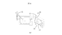
図2は、本発明に係る電力変換装置の鳥瞰図の一例である。
本発明による電力変換装置の実施例2における形態を以下に図を用いて説明する。
図1と共通の構成および同一の機能については、同一の参照番号を付してある。
パワー半導体PMは、順変換器部1、逆変換器部3、回生制動部9で構成されたモジュールである。パワー半導体にはケース15が取付けられた状態を示している。
パワー半導体PMは、図示していないネジにより冷却フィンに固定される。ドライブ回路8が搭載された基板PCBに設けられたスルーホールにパワー半導体のリード端子が貫通され半田(ソルダ)で電気的に接続される。
制御回路5が搭載された基板とドライブ回路8が搭載された基板PCBが電線により接続される。
本実施例では、パワー半導体のリード端子の先端形状がソルダピンの場合で説明したが、半田を使用しないプレスフィットピンの場合でも本発明の意図は変わらない。
冷却フィン11は、発熱体たるパワー半導体からの熱を伝導させ、図示していない冷却ファンによって冷却フィンに空気を送って熱交換させ、空冷方式によって放熱させている。
位置決めケース16は、パワー半導体PMを冷却フィンに取付ける際、パワー半導体の取付け位置を簡単に確定できるよう予めパワー半導体に合わせて開口部が設けられ、パワー半導体の搭載位置を固定するものである。
本実施例では、順変換器部1、逆変換器部3、回生制動部9で構成されたモジュールを例としたが、順変換器部1のみで構成されたパワー半導体と逆変換器部3と回生制動部9で構成されたパワー半導体2個を使用しても、順変換器部1と逆変換器部3と回生制動部9が各々個別に構成されたパワー半導体3個を使用しても発明の意図することは変わらない。
電力変換装置の筐体は、冷却フィン11、ケーシング12、電線引き出し板13、表面カバー14を備えて構成されている。
図3は、本発明に係る電力変換装置の位置決めケース16の鳥瞰図(第一の形態)である。
本発明による電力変換装置の実施例3における形態を以下に図を用いて説明する。
(a)は、パワー半導体PMに合わせて位置決めケース16に設けられた開口部Aの四辺に突起(バリア)17を設けた鳥瞰図である。
(b)は、位置決めケース16に設けられた開口部Aの二辺に突起(バリア)17を設けた鳥瞰図である。
(c)は、位置決めケース16に設けられた開口部Aに突起(バリア)を設けていない鳥瞰図である。
この突起17の高さh1は、パワー半導体PMの高さh2(図4(a)参照)より低くなるように設計されている。もちろん、突起17は、開口部Aの四辺と二辺に設けた場合、設けていない場合を示したが、突起を設ける辺の数に限定はない。
(d)は、(c)で説明した位置決めケース16とケース15を被せたパワー半導体を冷却フィンに搭載した状態の正面図と鳥瞰図である。
(e)は、(a)で説明した位置決めケースとケース15を被せたパワー半導体を冷却フィンに搭載した状態の正面図と鳥瞰図である。
位置決めケース16に設けられた四辺の突起17がパワー半導体PMに被せたケース15を押さえ、パワー半導体が破壊した際のモジュール内部の内圧上昇により、異常発熱に起因した炎が噴き出さないようにパワー半導体との隙間を小さくできることが分かる。
位置決めケースに設けられた開口部Aの四辺に突起を設けた(a)の方が、開口部Aに突起を設けていない(c)より、四辺の隙間をより小さくすることができ炎が噴き出る力を抑制する効果が大きい。
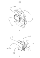
図4は、本発明に電力変換装置の係るケース15の鳥瞰図(第二の形態)である。
本発明による電力変換装置の実施例2における形態を以下に図を用いて説明する。
(a)は、パワー半導体PMの鳥瞰図の一例であり、リード端子が貫通していない69個の空きの開口部Bと1個のゲル注入用の開口部Cを有している。もちろん20本のリード端子が貫通している接触面Dにも隙間が存在する。
複数の開口部を設けている理由は、顧客専用のカスタムパワー半導体モジュールを製造する場合において、予め複数の開口部を設けておけば、リードフレームを自由な箇所に設けることができ、カスタムパワー半導体モジュールに対しても、標準のパワー半導体モジュールケースを共用できるという製造上の利点があるためである。
(b)は、一実施例におけるケース15の正面図と鳥瞰図である。パワー半導体の全てのリード端子位置に合わせてカバーに楕円形状と円形状の開口部を設けたものである。もちろん四角形状の開口部でもあっても構わない。
パワー半導体PMにケース15を被せても基板PCBと接続されるリード端子がカバーから突出するようにしており、当該ケース15を被せることにより開口部から噴出する炎を抑制することができるようにしたものである。
(c)は、他の実施例におけるケース15の正面図と鳥瞰図である。(b)の実施例に記載したカバーと異なるのは、基板PCBの裏面に搭載された部品、部品のリード足、パワー半導体を冷却フィンに取付けるためのネジとの電気的絶縁距離を確保するために両端に設けたはみ出し部分Eを有する点にある。本例については、詳細について後述する。
(d)は、パワー半導体のゲル注入用開口部Cを塞ぐ突起部(ボス)18を設けたケース15の正面図と裏面鳥瞰図である。鳥瞰図は、突起部18が識別できるようにケース15を裏面からみた状態を示している。突起部は、ゲル注入用開口部に挿入し易いように少しテーパーが設けられ、先端が細くなっている。もちろん四角形状の突起部(ボス)でもあっても構わない。
また、突起部の長さはパワー半導体のゲル注入用開口部の深さに従い設計すればよい。
(e)は、四辺に突起部19を設けたケースの正面図と鳥瞰図である。ケースの四辺に設けた突起部19は、ドライブ回路8が搭載された基板PCBの裏面に四辺に設けた突起部が接触することにより基板PCBの裏面が蓋の役割を果たし隙間をなくすことができるようにしたものである。もちろん突起部19は、四辺に限定されるものではなく、二辺でも効果がある。(b)から(d)における実施例のケースに対し、(e)の方法によればより効果的に隙間をなくすことができる。本例については、詳細について後述する。
(f)は、パワー半導体のリード端子の形状と本数に合わせ円形状の開口部Fを20個設けたケースの正面図と鳥瞰図である。開口部をリード端子の形状に合わせることにより、(b)から(e)における実施例のケースに対し、リード端子とケースの開口部との隙間をさらに小さくすることができる。
(g)は、パワー半導体にケースを取付ける状態を示した鳥瞰図である。ケースを矢印の方向に移動してパワー半導体に被せることにより、パワー半導体の20本のリード端子がケース15に設けられた開口部を貫通することにより、ケースでパワー半導体を覆うことが目的であり本発明の特徴である。また、ケースの厚みtは0.71mm以上に設計してある。
ケースは、パワー半導体を覆い、半導体モジュールが破壊した際に内部に発生する異常発熱による炎がリードフレームを貫通していない空きの開口部Bやゲル注入用の開口部Cから噴出し電力変換装置内部の他の部品などへの延焼による二次的延焼を誘発することを防止する。ケースは、例えばシリコンやプラスチィックなどの絶縁樹脂を用いて成型されたものである。扱い易さを考えれば、フレキシブル性の高いシリコンで成型したケースの方が作業性の面で現実的といえる。
図5は、本発明に係る電力変換装置の基板PCBとケース15の関係を示す鳥瞰図(第三の形態)である。
本発明による電力変換装置の実施例3における形態を以下に図を用いて説明する。
図2と共通の構成および同一の機能については、同一の参照番号を付してある。
(a)は、ドライブ回路8が搭載された基板PCBの図示していないスルーホールにパワー半導体のリード端子が貫通され半田で電気的に接続された状態を示す鳥瞰図である。
鳥瞰図は、基板の裏面から見た図である。
鳥瞰図は、基板の裏面から見た図である。
実装部品のリード足は、基板の図示していないスルーホールを貫通し基板の裏面から出た状態になる。裏面に出た代表的なリード足として20と21を示す。
冷却フィン上にケース15を被せたパワー半導体と位置決めケース16を取付け、基板のスルーホールにパワー半導体のリード端子を挿入して半田接続する。このため、図4(e)に示したケース15の四辺に設けた突起部19が基板の裏面に接触することにより、基板PCBの裏面が蓋の役割を果たし、隙間をなくすことができる。当然、基板の裏面と突起部が接触する部分には部品が実装されないように予め突起部を避けて基板の部品実装設計をしておけばよい。
(b)は、(a)において点線で囲んだ部分の拡大図である。
パワー半導体は図示していない冷却フィンに取付けネジで取付けられる。このネジの頭部と基板の裏面から出た実装部品のリード足20との距離dが予め規定された絶縁距離以上ない場合の実施例であり、パワー半導体に被せられたカバー15に設けた電気的絶縁距離確保用はみ出し部分Eによってリード足が囲まれるため、絶縁距離を縮退することができ電力変換装置の小型化も達成できる。
このようにすれば、開口部から噴出し電力変換装置内部の他の部品などへの延焼による二次的延焼を誘発することを防止できる。
図6は、本発明に係る電力変換装置のパワー半導体の開口部に絶縁樹脂を塗布した状態の図(第四の形態)である。
本発明による電力変換装置の実施例4における形態を以下に図を用いて説明する。
実施例1と異なるのは、成型されたケース15の代わりにシリコンあるいは絶縁樹脂を塗布して開口部Bあるいはゲル注入用の開口部Cを塞ぐ点にある。
(a)には、代表的塗布方法として、パワー半導体の開口部の一部に絶縁樹脂を一括塗布した箇所とポッティング塗布した箇所を例として記載している。これらの一方の方法(一括塗布かポッティング塗布)で開口部(BとC)を全て絶縁樹脂で塗布してもよいし、作業性を考慮して両方(一括塗布とポッティング塗布)を併用して全ての開口部(BとC)を塗布するのがより現実的である。もちろん、リードフレームが貫通している開口部Dの回りにシリコンあるいは絶縁樹脂を塗布してもよい。
(b)には、開口部やリード端子の関係を記載した当該パワー半導体の拡大鳥瞰図を示す。
以上の実施例で示したように、本発明により、半導体モジュールが破壊した際に内部に発生する異常発熱による炎がリードフレームを貫通していない空きの開口部やゲル注入用開口部などから噴き出し、電力変換装置内部の他の部品などへの延焼による電力変換装置の二次的延焼を防止することができる。
1…順変換器部、2…平滑用コンデンサ、3…逆変換器部、4…交流電動機、5…制御回路、6…冷却ファン、7…デジタル操作パネル、8…ドライブ回路、9…回生制動部、10…電力変換装置、11…冷却フィン、12…ケーシング、13…電線引き出し板、14…表面カバー、15…ケース、16…位置決めケース、17…突起、18…ケースに設けた突起部(ボス)、19…ケースに設けた突起部、20,21…部品のリード足、PM…パワー半導体、BR…回生制動抵抗、CT…電流検出器
Claims (14)
- パワー半導体と、
パワー半導体を冷却する冷却フィンと、
前記パワー半導体と前記冷却フィンとの間に配置され、前記パワー半導体の形状に合わせた開口部を備える第一のケースと、
前記パワー半導体に設けられたリード端子用の開口部を覆う第二のケースと、
を備える電力変換装置。 - 請求項1記載の電力変換装置であって、
前記第二のケースは、前記パワー半導体に設けられたゲル注入用の開口部を覆うことを特徴とする電力変換装置。 - 請求項1記載の電力変換装置であって、
前記第二のケースは、前記パワー半導体に設けられたゲル注入用の開口部を覆う突起を備えることを特徴とする電力変換装置。 - 請求項1記載の電力変換装置において、
前記第二のケースの少なくとも一辺に突起部が設けられていることを特徴とする電力変換装置。 - 請求項1記載の電力変換装置において、
前記第二のケースは、シリコンにより構成されることを特徴とする電力変換装置。 - 請求項1記載の電力変換装置において、
前記第二のケースは、プラスティック樹脂あるいは絶縁樹脂により構成されることを特徴とする電力変換装置。 - 請求項1記載の電力変換装置において、
前記第二のケースは、前記パワー半導体のリード端子が貫通する開口部があることを特徴とする電力変換装置。 - 請求項1記載の電力変換装置において、
前記第二のケースは、0.71mm以上の厚みであることを特徴とする電力変換装置。 - 請求項1記載の電力変換装置において、
前記第位置のケースは、前記パワー半導体の寸法に合わせた開口部を有することを特徴とする電力変換装置。 - 請求項9記載の電力変換装置において、
前記第二のケースの開口部は、少なくとも一辺に突起が設けられていることを特徴とする電力変換装置。 - 請求項10記載の電力変換装置において、
前記第二のケースの突起の高さは、前記パワー半導体の高さより低いことを特徴とする電力変換装置。 - 請求項1記載の電力変換装置において、
前記パワー半導体のリード端子用の開口部をシリコンまたは絶縁樹脂により塞ぐことを特徴とする電力変換装置。 - 請求項2記載の電力変換装置において、
前記パワー半導体のゲル注入用の開口部をシリコンまたは絶縁樹脂により塞ぐことを特徴とする電力変換装置。 - 請求項1記載の電力変換装置であって、
前記パワー半導体は複数のパワー半導体チップにより構成されることを特徴とする電力変換装置。
Priority Applications (2)
| Application Number | Priority Date | Filing Date | Title |
|---|---|---|---|
| CN201480034841.2A CN105308847B (zh) | 2013-06-19 | 2014-01-29 | 电力转换装置 |
| EP14813134.5A EP3012958B1 (en) | 2013-06-19 | 2014-01-29 | Power conversion device |
Applications Claiming Priority (2)
| Application Number | Priority Date | Filing Date | Title |
|---|---|---|---|
| JP2013128080A JP6082664B2 (ja) | 2013-06-19 | 2013-06-19 | 電力変換装置 |
| JP2013-128080 | 2013-06-19 |
Publications (1)
| Publication Number | Publication Date |
|---|---|
| WO2014203552A1 true WO2014203552A1 (ja) | 2014-12-24 |
Family
ID=52104301
Family Applications (1)
| Application Number | Title | Priority Date | Filing Date |
|---|---|---|---|
| PCT/JP2014/051886 WO2014203552A1 (ja) | 2013-06-19 | 2014-01-29 | 電力変換装置 |
Country Status (4)
| Country | Link |
|---|---|
| EP (1) | EP3012958B1 (ja) |
| JP (1) | JP6082664B2 (ja) |
| CN (1) | CN105308847B (ja) |
| WO (1) | WO2014203552A1 (ja) |
Cited By (1)
| Publication number | Priority date | Publication date | Assignee | Title |
|---|---|---|---|---|
| CN113396479A (zh) * | 2019-02-14 | 2021-09-14 | 株式会社日立产机系统 | 电力转换装置 |
Families Citing this family (2)
| Publication number | Priority date | Publication date | Assignee | Title |
|---|---|---|---|---|
| CN106505875B (zh) * | 2016-11-14 | 2019-05-28 | 广州瓦良格机器人科技有限公司 | 一种防腐防爆智能ipm变频模块 |
| JP7154907B2 (ja) | 2018-09-14 | 2022-10-18 | 株式会社東芝 | 半導体モジュール |
Citations (3)
| Publication number | Priority date | Publication date | Assignee | Title |
|---|---|---|---|---|
| JPH0636824A (ja) * | 1992-07-15 | 1994-02-10 | Matsushita Electric Ind Co Ltd | 防水・防塵コネクタ |
| JP2008288414A (ja) | 2007-05-18 | 2008-11-27 | Fuji Electric Device Technology Co Ltd | 半導体モジュール及び半導体モジュールの製造方法 |
| JP2012191849A (ja) * | 2007-04-20 | 2012-10-04 | Hitachi Industrial Equipment Systems Co Ltd | 電力変換装置及びパワーサイクル寿命予測方法 |
Family Cites Families (3)
| Publication number | Priority date | Publication date | Assignee | Title |
|---|---|---|---|---|
| FR2724283B1 (fr) * | 1994-09-02 | 1996-10-18 | Schneider Electric Sa | Variateur electronique de vitesse |
| US6147869A (en) * | 1997-11-24 | 2000-11-14 | International Rectifier Corp. | Adaptable planar module |
| JP4936149B2 (ja) * | 2007-01-18 | 2012-05-23 | 株式会社安川電機 | モータ制御装置 |
-
2013
- 2013-06-19 JP JP2013128080A patent/JP6082664B2/ja active Active
-
2014
- 2014-01-29 EP EP14813134.5A patent/EP3012958B1/en active Active
- 2014-01-29 CN CN201480034841.2A patent/CN105308847B/zh active Active
- 2014-01-29 WO PCT/JP2014/051886 patent/WO2014203552A1/ja active Application Filing
Patent Citations (3)
| Publication number | Priority date | Publication date | Assignee | Title |
|---|---|---|---|---|
| JPH0636824A (ja) * | 1992-07-15 | 1994-02-10 | Matsushita Electric Ind Co Ltd | 防水・防塵コネクタ |
| JP2012191849A (ja) * | 2007-04-20 | 2012-10-04 | Hitachi Industrial Equipment Systems Co Ltd | 電力変換装置及びパワーサイクル寿命予測方法 |
| JP2008288414A (ja) | 2007-05-18 | 2008-11-27 | Fuji Electric Device Technology Co Ltd | 半導体モジュール及び半導体モジュールの製造方法 |
Non-Patent Citations (2)
| Title |
|---|
| FUJI ELECTRIC REVIEW, vol. 85, no. 6, 2012, pages 426 - 429 |
| See also references of EP3012958A4 |
Cited By (2)
| Publication number | Priority date | Publication date | Assignee | Title |
|---|---|---|---|---|
| CN113396479A (zh) * | 2019-02-14 | 2021-09-14 | 株式会社日立产机系统 | 电力转换装置 |
| CN113396479B (zh) * | 2019-02-14 | 2023-09-22 | 株式会社日立产机系统 | 电力转换装置 |
Also Published As
| Publication number | Publication date |
|---|---|
| EP3012958A4 (en) | 2017-02-15 |
| JP6082664B2 (ja) | 2017-02-15 |
| EP3012958B1 (en) | 2020-04-01 |
| EP3012958A1 (en) | 2016-04-27 |
| CN105308847A (zh) | 2016-02-03 |
| JP2015006015A (ja) | 2015-01-08 |
| CN105308847B (zh) | 2018-04-13 |
Similar Documents
| Publication | Publication Date | Title |
|---|---|---|
| US7848104B2 (en) | Power module | |
| CN104742960B (zh) | 电子控制单元和具有电子控制单元的电动助力转向装置 | |
| JP5586866B2 (ja) | 電力変換装置 | |
| JP2017017975A (ja) | 電動コンプレッサ | |
| JP5974988B2 (ja) | 電子装置 | |
| JP6020379B2 (ja) | 半導体装置 | |
| JP2015099846A (ja) | 半導体装置および半導体装置の製造方法 | |
| JP6082664B2 (ja) | 電力変換装置 | |
| JP6647152B2 (ja) | Dcブラシレスモータおよび換気送風機 | |
| WO2014064822A1 (ja) | パワー半導体モジュールおよびこれを搭載した電力変換装置 | |
| JP4034766B2 (ja) | 回路基板及び電動送風機 | |
| JP3651406B2 (ja) | 電力変換装置 | |
| WO2016113858A1 (ja) | モータ及びモータの製造方法 | |
| JP6713246B2 (ja) | 電力変換装置 | |
| JP2002238260A (ja) | 半導体装置 | |
| JP2009232513A (ja) | 保護回路、半導体装置、電気機器 | |
| WO2017002693A1 (ja) | 電動コンプレッサ | |
| JP2006041407A (ja) | 半導体素子の温度検出方法及び電力変換装置 | |
| JP2013183544A (ja) | モータ配線構造 | |
| JP3566505B2 (ja) | インバータ装置 | |
| JP6439834B2 (ja) | 制御装置 | |
| JP5802798B2 (ja) | 電力変換装置 | |
| JP2019033197A (ja) | 回路基板装置における放熱構造 | |
| JP2014049610A (ja) | 回路基板 | |
| JP4930406B2 (ja) | パワー半導体装置及びこれを用いたインバータ装置 |
Legal Events
| Date | Code | Title | Description |
|---|---|---|---|
| WWE | Wipo information: entry into national phase |
Ref document number: 201480034841.2 Country of ref document: CN |
|
| 121 | Ep: the epo has been informed by wipo that ep was designated in this application |
Ref document number: 14813134 Country of ref document: EP Kind code of ref document: A1 |
|
| WWE | Wipo information: entry into national phase |
Ref document number: 2014813134 Country of ref document: EP |
|
| NENP | Non-entry into the national phase |
Ref country code: DE |