WO2014199573A1 - 光電変換素子および光電変換素子の作製方法 - Google Patents
光電変換素子および光電変換素子の作製方法 Download PDFInfo
- Publication number
- WO2014199573A1 WO2014199573A1 PCT/JP2014/002719 JP2014002719W WO2014199573A1 WO 2014199573 A1 WO2014199573 A1 WO 2014199573A1 JP 2014002719 W JP2014002719 W JP 2014002719W WO 2014199573 A1 WO2014199573 A1 WO 2014199573A1
- Authority
- WO
- WIPO (PCT)
- Prior art keywords
- layer
- photoelectric conversion
- light
- dielectric
- conversion element
- Prior art date
- Legal status (The legal status is an assumption and is not a legal conclusion. Google has not performed a legal analysis and makes no representation as to the accuracy of the status listed.)
- Ceased
Links
Images





Classifications
-
- H—ELECTRICITY
- H10—SEMICONDUCTOR DEVICES; ELECTRIC SOLID-STATE DEVICES NOT OTHERWISE PROVIDED FOR
- H10F—INORGANIC SEMICONDUCTOR DEVICES SENSITIVE TO INFRARED RADIATION, LIGHT, ELECTROMAGNETIC RADIATION OF SHORTER WAVELENGTH OR CORPUSCULAR RADIATION
- H10F77/00—Constructional details of devices covered by this subclass
- H10F77/40—Optical elements or arrangements
- H10F77/42—Optical elements or arrangements directly associated or integrated with photovoltaic cells, e.g. light-reflecting means or light-concentrating means
- H10F77/48—Back surface reflectors [BSR]
-
- H—ELECTRICITY
- H10—SEMICONDUCTOR DEVICES; ELECTRIC SOLID-STATE DEVICES NOT OTHERWISE PROVIDED FOR
- H10F—INORGANIC SEMICONDUCTOR DEVICES SENSITIVE TO INFRARED RADIATION, LIGHT, ELECTROMAGNETIC RADIATION OF SHORTER WAVELENGTH OR CORPUSCULAR RADIATION
- H10F10/00—Individual photovoltaic cells, e.g. solar cells
- H10F10/10—Individual photovoltaic cells, e.g. solar cells having potential barriers
- H10F10/17—Photovoltaic cells having only PIN junction potential barriers
-
- H—ELECTRICITY
- H10—SEMICONDUCTOR DEVICES; ELECTRIC SOLID-STATE DEVICES NOT OTHERWISE PROVIDED FOR
- H10F—INORGANIC SEMICONDUCTOR DEVICES SENSITIVE TO INFRARED RADIATION, LIGHT, ELECTROMAGNETIC RADIATION OF SHORTER WAVELENGTH OR CORPUSCULAR RADIATION
- H10F77/00—Constructional details of devices covered by this subclass
- H10F77/10—Semiconductor bodies
- H10F77/14—Shape of semiconductor bodies; Shapes, relative sizes or dispositions of semiconductor regions within semiconductor bodies
- H10F77/146—Superlattices; Multiple quantum well structures
-
- Y—GENERAL TAGGING OF NEW TECHNOLOGICAL DEVELOPMENTS; GENERAL TAGGING OF CROSS-SECTIONAL TECHNOLOGIES SPANNING OVER SEVERAL SECTIONS OF THE IPC; TECHNICAL SUBJECTS COVERED BY FORMER USPC CROSS-REFERENCE ART COLLECTIONS [XRACs] AND DIGESTS
- Y02—TECHNOLOGIES OR APPLICATIONS FOR MITIGATION OR ADAPTATION AGAINST CLIMATE CHANGE
- Y02E—REDUCTION OF GREENHOUSE GAS [GHG] EMISSIONS, RELATED TO ENERGY GENERATION, TRANSMISSION OR DISTRIBUTION
- Y02E10/00—Energy generation through renewable energy sources
- Y02E10/50—Photovoltaic [PV] energy
- Y02E10/52—PV systems with concentrators
-
- Y—GENERAL TAGGING OF NEW TECHNOLOGICAL DEVELOPMENTS; GENERAL TAGGING OF CROSS-SECTIONAL TECHNOLOGIES SPANNING OVER SEVERAL SECTIONS OF THE IPC; TECHNICAL SUBJECTS COVERED BY FORMER USPC CROSS-REFERENCE ART COLLECTIONS [XRACs] AND DIGESTS
- Y02—TECHNOLOGIES OR APPLICATIONS FOR MITIGATION OR ADAPTATION AGAINST CLIMATE CHANGE
- Y02E—REDUCTION OF GREENHOUSE GAS [GHG] EMISSIONS, RELATED TO ENERGY GENERATION, TRANSMISSION OR DISTRIBUTION
- Y02E10/00—Energy generation through renewable energy sources
- Y02E10/50—Photovoltaic [PV] energy
- Y02E10/548—Amorphous silicon PV cells
Definitions
- the present invention relates to a photoelectric conversion element that converts light energy into electric energy by photoelectric conversion.
- a texture structure is produced on the front surface and / or back surface of the photoelectric conversion layer, and incident light and reflected light are scattered on the front surface and back surface of the photoelectric conversion layer, respectively, so that the optical path length in the photoelectric conversion layer is increased.
- incident light and reflected light are scattered on the front surface and back surface of the photoelectric conversion layer, respectively, so that the optical path length in the photoelectric conversion layer is increased.
- a technique for processing a periodic fine structure in a photoelectric conversion element is known. In this case, the light to be transmitted through the photoelectric conversion layer is diffracted by the periodic fine pattern. Therefore, the light can be confined in the photoelectric conversion layer by setting a condition in which the reflected light is totally reflected in the photoelectric conversion layer, so that the photoelectric conversion efficiency can be improved.
- JP-A-61-288473 Japanese Patent Laid-Open No. 4-133360 JP 2000-294818 A Special table 2009-533875 gazette
- the texture structure is formed on the front surface and / or back surface of the photoelectric conversion layer
- a relatively large amount of light leaks outside the photoelectric conversion element without being reflected toward the photoelectric conversion layer.
- the recombination speed of carriers greatly increases in the surface layer of the solar cell, which causes a problem that the photoelectric conversion performance decreases.
- the present invention has been made in view of such problems, and an object thereof is to provide a technique capable of increasing the photoelectric conversion efficiency of the photoelectric conversion element.
- An embodiment of the present invention is a photoelectric conversion element.
- the photoelectric conversion element includes a photoelectric conversion layer, a metal film provided on a side opposite to a light receiving surface side of the photoelectric conversion layer, and a plurality of provided on a main surface of the metal film on the photoelectric conversion layer side.
- the plurality of dielectrics are arranged in a square lattice pattern.
- a substrate may be provided between the photoelectric conversion layer and the light reflection layer, and the metal film and the dielectric may be in contact with the back surface of the substrate.
- the photoelectric conversion layer includes a first semiconductor layer located on a light receiving surface side, a second semiconductor layer having a conductivity type opposite to the conductivity type of the first semiconductor layer, the first semiconductor layer, and the first semiconductor layer.
- One or more first semiconductor regions provided between the first semiconductor layer and the second semiconductor layer and having a band gap greater than or equal to a band gap of the first semiconductor layer and the second semiconductor layer, and the first semiconductor
- a quantum structure layer having one or more second semiconductor regions having a band gap less than or equal to that of the second semiconductor layer.
- the sum of the length of one side of the exposed portion of the dielectric and the interval between the adjacent dielectrics may be 600 nm to 1000 nm.
- the ratio of the total area of the exposed portion of the dielectric to the entire main surface of the light reflecting layer is 0.4 to 0.00. 8 may be sufficient.
- the shape of the dielectric material in a cross section orthogonal to the main surface of the light reflecting layer may be a trapezoidal shape having a long side on the photoelectric conversion layer side.
- the photoelectric conversion element manufacturing method includes a step of applying a dielectric material on the side opposite to the light receiving surface side of the photoelectric conversion layer, and pressing a mold having a pattern in which concave portions are arranged in a square lattice shape from above the dielectric material. And forming a plurality of dielectrics on the side opposite to the light receiving surface side of the photoelectric conversion layer, and forming a metal film from above the plurality of dielectrics, the inner wall surface of the recess
- the taper shape is such that the bottom surface of the recess is narrower than the opening of the recess.
- the photoelectric conversion efficiency of the photoelectric conversion element can be increased.
- FIG. 1 is a cross-sectional view illustrating a schematic configuration of a photoelectric conversion element 10 according to an embodiment.
- the photoelectric conversion element 10 includes a first electrode 20, a first contact layer 30, a window layer 40, a first semiconductor layer 50, a quantum structure layer 60, a second semiconductor layer 70, a second contact layer 80, a substrate 90, and a light reflecting layer. 100 and the second electrode 110.
- the photoelectric conversion element 10 is a group III-V compound semiconductor solar cell, and examples of the “photoelectric conversion layer” include “first semiconductor layer 50, quantum structure layer 60, and second semiconductor layer 70”.
- the present invention is not limited to this, and a crystalline Si solar cell, a microcrystalline Si solar cell, an amorphous Si solar cell, an amorphous SiGe solar cell, a CIGS solar cell, or the like may be used.
- the first electrode 20 is a surface electrode provided on the light receiving surface side of the window layer 40, and is formed on the first contact layer 30 described later.
- the first electrode 20 is a p-type electrode in the present embodiment.
- the first electrode 20 only needs to be in ohmic contact with the first contact layer 30.
- an AuZn alloy or an Ag / Au laminated thin film can be used.
- the first contact layer 30 is provided in the peripheral region of the light receiving surface of the window layer 40.
- the first contact layer 30 is a p-type contact layer, and is formed of a compound semiconductor material composed of a Group III element and a Group V element of the periodic table such as GaAs, AlGaAs, InGaP, for example.
- the doping amount of the p-type impurity in the first contact layer 30 is, for example, 1 ⁇ 10 19 cm ⁇ 3 .
- the window layer 40 is a semiconductor layer that prevents carriers generated in the first semiconductor layer from recombining and deactivating on the surface of the first semiconductor layer.
- the semiconductor layer in the window layer 40 is not particularly limited as long as it transmits light sufficiently and has a low surface recombination velocity.
- a group III element and a group V element in the periodic table such as AlGaAs and InGaP.
- the doping amount of the p-type impurity in the window layer 40 is, for example, 5 ⁇ 10 18 cm ⁇ 3 .
- An antireflection film may be further formed on the light receiving surface side surface of the window layer 40.
- the antireflection film is made of a dielectric having a refractive index higher than that of air and lower than that of the window layer 40.
- the dielectric in the antireflection film is not particularly limited as long as it sufficiently transmits light and the refractive index satisfies the above conditions.
- silicon oxide, zinc oxide, aluminum oxide, magnesium fluoride, titanium oxide, Zinc sulfide or the like can be preferably used.
- the first semiconductor layer 50 is a p-type compound semiconductor layer formed of the same compound semiconductor material as the first contact layer 30.
- the doping amount of the p-type impurity in the first semiconductor layer 50 is, for example, 2 ⁇ 10 18 cm ⁇ 3 .
- the quantum structure layer 60 includes a first semiconductor region having a band gap greater than or equal to that of the first semiconductor layer 50 and the second semiconductor layer 70 described later, and a band gap less than or equal to the band gap of the first semiconductor layer 50 and the second semiconductor layer 70. It has a quantum well structure in which second semiconductor regions having band gaps are alternately stacked.
- the first semiconductor region includes one or more types of semiconductor layers, and the energy gap of the first semiconductor region is from the portion where the first semiconductor region and the first semiconductor layer 50 are in contact toward the center of the first semiconductor region. It can be changed step by step, and can also be changed continuously.
- the second semiconductor region includes one or more types of semiconductor layers, and the energy gap of the second semiconductor region is stepped from the portion where the second semiconductor region and the first semiconductor region are in contact toward the center of the second semiconductor region. It can also be changed continuously.
- the first semiconductor region and the second semiconductor region are formed of intrinsic semiconductor layers, but may be doped with impurities having a first conductivity type (for example, p-type) or a second conductivity type (for example, n-type). Good.
- the compound semiconductor material forming the quantum structure layer 60 for example, a compound semiconductor material composed of a Group III element and a Group V element of the periodic table such as InGaAs, InAs, GNAAs, and GaAsP can be used.
- the second semiconductor layer 70 is an n-type compound semiconductor layer stacked on the main surface of the quantum structure layer 60 on the side opposite to the light receiving surface side.
- the second semiconductor layer 70 is formed of a compound semiconductor material composed of a Group III element and a Group V element of the periodic table such as GaAs, AlGaAs, InGaP, for example.
- the doping amount of the n-type impurity in the second semiconductor layer 70 is, for example, 2 ⁇ 10 18 cm ⁇ 3 .
- the second contact layer 80 is stacked on the main surface of the second semiconductor layer 70 on the side opposite to the light receiving surface side.
- the second contact layer 80 is an n-type contact layer and is formed of the same compound semiconductor material as that of the second semiconductor layer 70.
- the doping amount of the n-type impurity in the second contact layer 80 is, for example, 2 ⁇ 10 18 cm ⁇ 3 .
- the second contact layer 80 is provided with a step so that the substrate 90 side is wide, and has an exposed surface exposed to the light receiving surface side.
- the substrate 90 is used as a substrate for semiconductor layer growth, for example, a semiconductor substrate such as GaAs or Ge is used.
- the substrate 90 is a semi-insulating GaAs substrate.
- the substrate 90 may be removed by dissolution or peeling after the growth of the semiconductor layer.
- the light reflection layer 100 described later is directly laminated on the second contact layer 80.
- the light reflecting layer 100 is provided on the side opposite to the light receiving surface of the photoelectric conversion element 10. In the present embodiment, the light reflecting layer 100 is provided in contact with the substrate 90. Details of the light reflecting layer 100 will be described later.
- the second electrode 110 is an n-type counter electrode provided on the exposed surface of the second contact layer 80.
- As the second electrode 110 for example, Au, Ag, Al, Cu, or an alloy containing these metals can be used.
- the second electrode 110 only needs to be electrically joined to the second semiconductor layer 70, and may be formed on the back surface of the substrate 90.
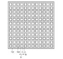
- FIG. 2 is a plan view of the light reflecting layer 100 when viewed from the light receiving surface side of the photoelectric conversion element 10. Details of the light reflecting layer 100 will be described with reference to FIGS. 1 and 2.
- the light reflecting layer 100 includes a metal film 102 and a dielectric 104.
- the metal film 102 is provided in contact with the substrate 90.
- the metal constituting the metal film 102 is not particularly limited as long as it is a metal material having a scattering property in the wavelength region of light in which the quantum structure layer 60 is insufficiently absorbed.
- Ag, Al, Au, Cu or an alloy of these metals can be used.
- the thickness of the metal film 102 is, for example, 50 nm to 2000 nm.
- the metal film 102 can also serve as the second electrode.
- a plurality of recesses 112 are formed on the main surface of the metal film 102 on the substrate 90 side.
- the shape of the recess 112 is a quadrangular prism.
- the depth of the recess 112 is preferably 150 nm to 400 nm, and more preferably 200 nm to 300 nm.
- the plurality of recesses 112 are arranged in a square lattice pattern.
- Each recess 112 is filled with a dielectric 104, and a plurality of dielectrics 104 are also arranged in a square lattice.
- the shape of the dielectric 104 is defined by the recess 112, and is a quadrangular prism like the recess 112. As shown in FIG.
- the upper surface of the dielectric 104 is exposed on the main surface of the light reflecting layer 100 on the substrate 90 side, and the shape thereof is a square shape.
- the material for forming the dielectric 104 may be a transparent material having a refractive index lower than that of the layer in contact with the light reflecting layer 100 (in this embodiment, the substrate 90).
- Epoxy resin, acrylic resin, polystyrene, cycloolefin Examples thereof include polymers, fluororesins, alumina, ZnO, and SiO 2 .
- the square lattice shape is not limited to the case where the lattice unit is a square, and the ratio L2 / L1 is greater than 1 and less than or equal to 1.1 when the short side of the unit lattice is L1 and the long side is L2. Cases are also included in the “square lattice”.
- the quantum structure layer 60 In the light reflection layer 100, light is reflected in an angled state with respect to the normal of the main surface of the quantum structure layer 60. Thereby, the optical path length of the reflected light in the quantum structure layer 60 can be increased, and as a result, the quantum structure layer 60 can absorb light efficiently.
- the refractive index at a wavelength of 1000 nm is about 3.5, and is 16.6 degrees with respect to the normal of the boundary between GaAs and the atmosphere (16 with respect to the normal)
- the incident light diffusely reflected on the back surface of the substrate 90 at a larger angle is not radiated into the atmosphere but on the surface of the window layer 40.
- a conical region formed by a region smaller than .6 degrees is called an escape cone. It is totally reflected again and can be confined in the photoelectric conversion element 10.
- the sum L (square lattice period L) of the length D of one side of the exposed portion of the dielectric 104 and the interval W between the adjacent dielectrics 104 is preferably 600 nm to 1000 nm. As shown in FIG. 2, when the main surface of the light reflecting layer 100 is viewed in plan, the ratio of the total area S of the exposed portion of each dielectric 104 to the entire main surface of the light reflecting layer is 0.4. It is preferable that the value be 0.8. By making the period L and the total area S of the square lattice within the above ranges, the light reflection in the light reflection layer 100 can be made more effective.
- the photoelectric conversion efficiency can be further increased by increasing the optical path length of the reflected light by the light reflecting layer 100.
- a single crystal silicon wafer 200 is prepared.
- a silicon dioxide layer 202 is formed on one main surface of the single crystal silicon wafer 200 by thermal oxidation.
- the thickness of the silicon dioxide layer 202 is, for example, 100 nm.
- an electron beam drawing resist 204 is applied on the silicon dioxide layer 202.
- An example of the resist 204 is ZEP-520A manufactured by Nippon Zeon.
- the thickness of the resist 204 is 400 nm, for example.
- the resist 204 is developed into a pattern arranged in a square lattice by electron beam drawing.
- dry etching of the silicon dioxide layer 202 is performed by using the resist 204 as a mask and using Ar and CHF 3 as etching gases, and the silicon dioxide layer 202 having the same pattern as the resist 204 is formed.
- the pattern is formed.
- the resist 204 by interposing a silicon dioxide layer 202 between the single crystal silicon wafer 200 and the resist 204, in the dry etching of the single crystal silicon wafer 200 described later, the resist The silicon dioxide layer 202 having an etching rate lower than 204 remains as a mask. Thereby, the groove
- the resist 204 is removed by O 2 ashing.
- a molding material 310 is applied on the original mold 300.
- the molding material 310 for example, polydimethylsiloxane (PDMS) is used.
- the thickness of the mold material 310 after application is, for example, 0.5 mm.
- the mold material 310 is thermally cured, and then peeled off from the original mold 300 to produce a soft mold 320.
- a UV curable resin 330 is applied as a dielectric material to the back surface of the substrate 90 provided on the back surface side of the quantum structure layer.
- the thickness of the UV curable resin 330 is, for example, 600 nm.
- the soft mold 320 is pressed from above the UV curable resin 330.
- the pressure when pressing the soft mold 320 is, for example, 3 kPa.
- the soft mold 320 is peeled off from the UV curable resin 330.
- the residual film adhering to the back surface of the substrate 90 is removed by O 2 ashing, and a dielectric 104 having a quadrangular shape is formed.
- silver is evaporated from above the dielectric 104 to form a metal film 102.
- the light reflecting layer 100 having the metal film 102 and the dielectric 104 can be formed.
- the photoelectric conversion element according to the modified example is the same as the photoelectric conversion element of the embodiment, except that the manufacturing method and shape of the dielectric 104 are different.
- the silicon dioxide layer 202 is used as a mask, and Ar is used as an etching agent in addition to Cl 2 .
- the silicon dioxide layer 202 is intentionally cut by a physical action, and the inner wall surface of the recess formed in the original mold 300 becomes tapered so that the bottom surface of the recess is narrower than the opening of the recess.
- a soft mold 320 as shown in FIG. 8B is obtained by using the master mold 300 thus obtained through the same steps as in the embodiment.
- the shape in the cross section orthogonal to the main surface of the light reflecting layer 100 is long on the substrate 90 side.
- a trapezoidal dielectric 104 is formed.
- the deformation of the UV curable resin 303 when the soft mold 320 is pressed for transfer is reduced, so that the dielectric 104 is prevented from being out of shape,
- the transfer accuracy of the dielectric 104 can be increased.
- a photoelectric conversion element (quantum well type solar cell) was manufactured using a metal organic chemical vapor deposition (MOVPE) method. Specifically, an insulative GaAs substrate (carrier concentration: 1 ⁇ 10 7 cm ⁇ 3 ) having a mirror surface on both sides and having a thickness of 350 ⁇ m is put into a MOVPE apparatus, and at a temperature of 600 ° C. and a pressure of 10 kPa, trimethylgallium, trimethylindium, Crystal growth was performed using tertiary butylarsine and tertiary butylphosphine as raw materials and hydrogen as a carrier gas.
- MOVPE metal organic chemical vapor deposition
- n-type GaAs carrier concentration: 2 ⁇ 10 18 cm ⁇ 3
- base layer n-type GaAs
- an i-phase GaAs film is first formed to a thickness of 0.1 ⁇ m, and then, as a quantum structure, a well layer In 0.17 Ga 0.83 As (8.54 nm), a barrier layer GaAs 0.78 P 20 layers of 0.22 (18.1 nm) were stacked.
- p-type GaAs carrier concentration: 2 ⁇ 10 18 cm ⁇ 3
- p-type In 0.49 Ga 0.51 P carrier is used as the window layer
- Concentration: 5 ⁇ 10 18 cm ⁇ 3 was 0.04 ⁇ m
- p-type GaAs carrier concentration: 1 ⁇ 10 19 cm ⁇ 3
- the grown epitaxial layer was etched away to the second semiconductor layer using the quantum well layer portion as a mask, AuGe / Ni was vapor-deposited as the second electrode, and heat treatment was performed at 380 ° C. in nitrogen. Further, a resist with an electrode pattern opened is formed on the first contact layer, and after depositing Ag / Au, the first electrode (surface electrode) is formed by the lift-off method, and the electrode is formed using the first electrode as a mask. The portion of the first contact layer that was not removed was removed by etching.
- Examples 2 to 4 Comparative Examples 1 to 9
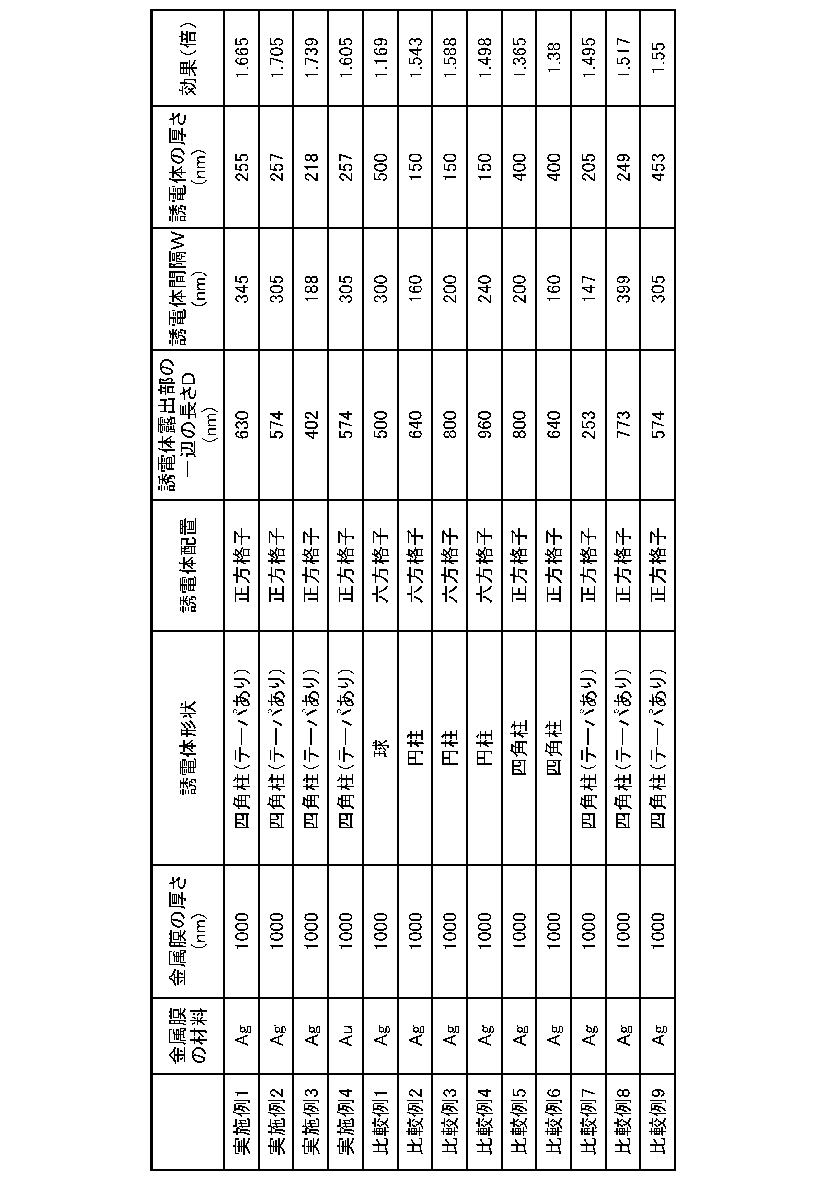
- the photoelectric conversion elements of Examples 2 to 4 and Comparative Examples 1 to 9 were prepared in the same manner as the photoelectric conversion element of Example 1 described above, except for the conditions shown in Table 1.
- the spectral sensitivity measurement device is a two-lamp type of xenon lamp and halogen lamp. It irradiates the solar cell with monochromatic light of 300 to 1100 nm spectrally separated by a monochromator and performs in AC mode. From the number of photons and the photocurrent value of each wavelength The quantum yield was calculated. In addition, the quantum yield was calculated in the same manner for a reference photoelectric conversion element in which a light reflection layer was not provided on the back surface of the insulating GaAs substrate. How many times the quantum yield in the wavelength range (900 to 1100 nm) due to the quantum structure layer of each photoelectric conversion element of Examples 1 to 4 and Comparative Examples 1 to 9 is larger than the reference photoelectric conversion element Calculated and listed in Table 1 as effects.
- FIG. 9 shows the relationship between the ratio of the total area of the exposed portion of the dielectric to the entire main surface of the light reflecting layer and the effect of improving the quantum yield.
- FIG. 9 confirms that the effect of improving the quantum yield is remarkably large when the ratio of the total area of the exposed portion of the dielectric to the entire main surface of the light reflecting layer is 0.4 to 0.8. It was done.
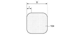
- the term “rectangular shape” of the shape of the exposed portion of the dielectric 104 is not limited to the shape having a 90 ° corner, and when the light reflecting layer is viewed in plan as shown in FIG. The case where the corner of the body 104 is rounded is also included. However, the ratio of the length D of one side of the dielectric 104 to the width r in the length direction of the one side of the rounded portion, D: r is in the range of 1: 0 to 1: 0.2. .
- the present invention can be used for a photoelectric conversion element and a method for manufacturing the photoelectric conversion element.
Landscapes
- Photovoltaic Devices (AREA)
Abstract
本発明のある態様の光電変換素子10では、受光側とは反対側の基板90の主表面に光反射層100が設けられている。光反射層100は、金属膜102および誘電体104を含む。金属膜102は、基板90に接して設けられている。金属膜102を構成する金属としは、例えば、Ag、Al、Au、Cuまたはこれらの金属の合金が挙げられる。金属膜102の量子構造層60の側の主表面には、四角柱状の複数の凹部112が形成されている。複数の凹部112は、光反射層100の主表面を平面視したときに正方格子状になるように配列されており、各凹部112に誘電体104が充填されている。
Description
本発明は、光電変換により光エネルギーを電気エネルギーに変換する光電変換素子に関する。
太陽電池などの光電変換素子は、省資源化や低コスト化を図るために光電変換層のさらなる薄膜化が望まれている。しかしながら、単純に光電変換層を薄膜化しただけでは光電変換層における光吸収量が減少し、光電変換効率が低下してしまう。そのため、光電変換層における吸収量を増加させる技術の開発が不可欠である。
このような技術として、光電変換層の表面および/または裏面にテクスチャ構造を作製し、光電変換層の表面、裏面において、それぞれ入射光、反射光を散乱させて、光電変換層での光路長を増大させる方法がある。また、光電変換素子に周期的な微細構造を加工する技術が知られている。この場合には、光電変換層を透過しようとする光が周期的な微細パターンによって回折する。そこで、反射した光が光電変換層において全反射する条件を微細パターンに設定することで光を光電変換層内に閉じ込めることができ、これにより光電変換効率の向上が図られる。
しかしながら、従来のように光電変換層の表面および/または裏面にテクスチャ構造を作製する構成では、比較的多くの光が光電変換層に向けて反射されずに光電変換素子の外部に漏れていた。また、太陽電池表面にテクスチャ構造や周期的な微細構造を設けると、太陽電池表層においてキャリアの再結合速度が大きく増加するため、光電変換性能が低下する、といった課題が生じる。
本発明はこうした課題に鑑みてなされたものであり、その目的は、光電変換素子の光電変換効率を高めることができる技術の提供にある。
本発明のある態様は、光電変換素子である。当該光電変換素子は、光電変換層と、前記光電変換層の受光面側とは反対側に設けられている金属膜と、前記金属膜の前記光電変換層の側の主表面に設けられた複数の凹部にそれぞれ充填された誘電体と、を有する光反射層と、を備え、前記光電変換層と対向する前記光反射層の主表面を平面視したときに前記誘電体の露出部が四角形状であり、前記光電変換層と対向する前記光反射層の主表面を平面視したときに複数の前記誘電体が正方格子状に配列されていることを特徴とする。
上記態様の光電変換素子において、前記光電変換層と前記光反射層との間に基板が設けられ、前記基板の裏面に前記金属膜および前記誘電体が接していてもよい。前記光電変換層が、受光面側に位置する第1の半導体層と、前記第1の半導体層の導電型と反対の導電型の第2の半導体層と、前記第1の半導体層と前記第2の半導体層との間に設けられており、前記第1の半導体層および前記第2の半導体層のバンドギャップ以上のバンドギャップを有する1以上の第1の半導体領域と、前記第1の半導体層及び前記第2の半導体層のバンドギャップ以下のバンドギャップを有する1以上の第2の半導体領域と、を有する量子構造層とから構成されていてもよい。誘電体の露出部の1辺の長さと、隣接する誘電体の間隔の和が600nm~1000nmであってもよい。前記光電変換層と対向する前記光反射層の主表面を平面視したときに、光反射層の主表面全体に対して前記誘電体の露出部の総面積が占める割合が0.4~0.8であってもよい。また、前記光反射層の主表面と直交する断面における前記誘電体の形状が、前記光電変換層側を長辺とする台形状であってもよい。
本発明の他の態様は、光電変換素子の作製方法である。当該光電変換素子の作製方法は、光電変換層の受光面側とは反対側に誘電材料を塗布する工程と、前記誘電材料の上から正方格子状に凹部が配列されたパターンを有するモールドを押圧して、前記光電変換層の受光面側とは反対側に複数の誘電体を形成する工程と、前記複数の誘電体の上から金属膜を形成する工程と、を備え、前記凹部の内壁面が、前記凹部の開口に比べて凹部の底面が狭くなるようなテーパ状であることを特徴とする。
なお、上述した各要素を適宜組み合わせたものも、本件特許出願によって特許による保護を求める発明の範囲に含まれうる。
本発明によれば、光電変換素子の光電変換効率を高めることができる。
以下、本発明の実施の形態を図面を参照して説明する。なお、すべての図面において、同様な構成要素には同様の符号を付し、適宜説明を省略する。
(実施の形態)
図1は、実施の形態に係る光電変換素子10の概略構成を示す断面図である。光電変換素子10は、第1電極20、第1コンタクト層30、窓層40、第1半導体層50、量子構造層60、第2半導体層70、第2コンタクト層80、基板90、光反射層100および第2電極110を有する。本実施の形態では、光電変換素子10はIII-V族化合物半導体太陽電池であり、「光電変換層」の一例として、「第1半導体層50、量子構造層60、および第2半導体層70」を有するが、これに限らず、結晶Si太陽電池、微結晶Si太陽電池、アモルファスSi太陽電池、アモルファスSiGe太陽電池、CIGS太陽電池などでもよい。
図1は、実施の形態に係る光電変換素子10の概略構成を示す断面図である。光電変換素子10は、第1電極20、第1コンタクト層30、窓層40、第1半導体層50、量子構造層60、第2半導体層70、第2コンタクト層80、基板90、光反射層100および第2電極110を有する。本実施の形態では、光電変換素子10はIII-V族化合物半導体太陽電池であり、「光電変換層」の一例として、「第1半導体層50、量子構造層60、および第2半導体層70」を有するが、これに限らず、結晶Si太陽電池、微結晶Si太陽電池、アモルファスSi太陽電池、アモルファスSiGe太陽電池、CIGS太陽電池などでもよい。
第1電極20は、窓層40の受光面側に設けられている表面電極であり、後述する第1コンタクト層30の上に形成されている。第1電極20は、本実施の形態では、p型電極である。第1電極20は、第1コンタクト層30とオーミックなコンタクトが取れればよく、たとえば、AuZn合金や、Ag/Auの積層薄膜などを用いることができる。
第1コンタクト層30は、窓層40の受光面の周縁領域に設けられている。第1コンタクト層30は、p型のコンタクト層であり、例えば、GaAs、AlGaAs、InGaPなどの周期表の第III族元素および第V族元素からなる化合物半導体材料により形成される。第1コンタクト層30におけるp型不純物のドープ量は、例えば、1×1019cm-3である。
窓層40は、第1半導体層で生成したキャリアが第1半導体層表面で再結合し失活するのを防ぐ半導体層である。窓層40における半導体層としては、光を十分に透過し、表面再結合速度が小さいものであれば特に限定されないが、例えば、AlGaAs、InGaPなどの周期表の第III族元素および第V族元素からなる化合物半導体材料により形成される。窓層40におけるp型不純物のドープ量は、例えば、5×1018cm-3である。窓層40の受光面側の表面にさらに反射防止膜を形成してもよい。反射防止膜は、屈折率が空気よりも高く、かつ窓層40より低い誘電体からなる。反射防止膜における誘電体としては、光を十分に透過し、屈折率が上記条件を満たすものであれば特に限定されないが、例えば、酸化ケイ素、酸化亜鉛、酸化アルミニウム、フッ化マグネシウム、酸化チタン、硫化亜鉛等を好適に用いることができる。
第1半導体層50は、第1コンタクト層30と同様な化合物半導体材料により形成されるp型化合物半導体層である。第1半導体層50におけるp型不純物のドープ量は、例えば、2×1018cm-3である。
量子構造層60は、第1半導体層50および後述する第2半導体層70のバンドギャップ以上のバンドギャップを有する第1半導体領域と、第1半導体層50および第2半導体層70のバンドギャップ以下のバンドギャップを有する第2の半導体領域とが交互に積層された量子井戸構造を有する。
第1半導体領域には1種類以上の半導体層が含まれ、第1半導体領域のエネルギーギャップは、第1半導体領域と前記第1半導体層50が接する部分から第1半導体領域の中心方向へ向かって段階的に変化させることができ、さらに連続的に変化させることもできる。
第2半導体領域には1種類以上の半導体層が含まれ、第2半導体領域のエネルギーギャップは、第2半導体領域と第1半導体領域が接する部分から第2半導体領域の中心方向へ向かって段階的に変化させることができ、さらに連続的に変化させることもできる。
本実施の形態では、第1半導体領域および第2半導体領域は真性半導体層からなるが、第1導電型(例えばp型)や第2導電型(例えばn型)を有する不純物をドープしてもよい。
本実施の形態では、第1半導体領域および第2半導体領域は真性半導体層からなるが、第1導電型(例えばp型)や第2導電型(例えばn型)を有する不純物をドープしてもよい。
量子構造層60を形成する化合物半導体材料として、例えばInGaAs、InAs、GaNAs、GaAsPなどの周期表の第III族元素および第V族元素からなる化合物半導体材料を用いることができる。
第2半導体層70は、受光面側とは反対側の量子構造層60の主表面に積層されたn型化合物半導体層である。第2半導体層70は、例えば、GaAs、AlGaAs、InGaPなどの周期表の第III族元素および第V族元素からなる化合物半導体材料により形成される。第2半導体層70におけるn型不純物のドープ量は、例えば、2×1018cm-3である。
第2コンタクト層80は、受光面側とは反対側の第2半導体層70の主表面に積層されている。第2コンタクト層80は、n型のコンタクト層であり、第2半導体層70と同様な化合物半導体材料により形成される。第2コンタクト層80におけるn型不純物のドープ量は、例えば、2×1018cm-3である。第2コンタクト層80には、基板90側が幅広になるような段差が設けられており、受光面側に露出する露出面を有する。
基板90は、半導体層成長用の基板として利用される場合には、例えば、GaAsやGe等の半導体基板が用いられる。本実施の形態では、基板90は半絶縁性のGaAs基板である。なお、基板90は、半導体層成長後に、溶解ないしは剥離により取り除いてもよい。この場合、後述する光反射層100は、第2コンタクト層80に直に積層される。
光反射層100は、光電変換素子10の受光面とは反対側に設けられている。本実施の形態では、光反射層100は、基板90に接して設けられている。光反射層100の詳細については後述する。
第2電極110は、第2コンタクト層80の露出面に設けられているn型対向電極である。第2電極110として、例えば、Au、Ag、Al、Cuまたはこれらの金属を含む合金を用いることができる。第2電極110は、第2半導体層70と電気的に接合していればよく、基板90の裏面に形成されていてもよい。
(光反射層)
図2は、光反射層100を光電変換素子10の受光面側から平面視したときの平面図である。図1および図2を参照しながら、光反射層100の詳細について説明する。
図2は、光反射層100を光電変換素子10の受光面側から平面視したときの平面図である。図1および図2を参照しながら、光反射層100の詳細について説明する。
光反射層100は、金属膜102および誘電体104を含む。金属膜102は、基板90に接して設けられている。金属膜102を構成する金属は、量子構造層60の吸収が不十分である光の波長領域において、散乱性を有する金属材料であればよく、特に限定されないが、例えば、Ag、Al、Au、Cuまたはこれらの金属の合金が挙げられる。金属膜102の厚さは、例えば、50nm~2000nmである。なお、第2電極110を別途設ける代わりに、金属膜102に第2電極を兼ねさせることもできる。
金属膜102の基板90の側の主表面には、複数の凹部112が形成されている。凹部112の形状は、四角柱状である。凹部112の深さは、150nm~400nmが好ましく、200nm~300nmの範囲がより好ましい。図2に示すように、複数の凹部112は、正方格子状に配列されている。各凹部112に誘電体104が充填されており、複数の誘電体104も正方格子状に配列されている。誘電体104の形状は凹部112で規定され、凹部112と同様に四角柱である。図2に示すように、光反射層100の基板90の側の主表面において、誘電体104の上面が露出しており、その形は四角形状である。誘電体104を形成する材料としては、光反射層100と接する層(本実施の形態では、基板90)より屈折率が低い透明な材料であればよく、エポキシ樹脂、アクリル樹脂、ポリスチレン、シクロオレフィンポリマー、フッ素樹脂、アルミナ、ZnO、SiO2などが挙げられる。なお、正方格子状とは、格子単位が正方形である場合に限られず、単位格子の短辺をL1と長辺をL2としたとき比L2/L1が1より大きく1.1以下の範囲に当てはまる場合も「正方格子状」に含まれる。
光反射層100において、量子構造層60の主表面の法線に対して角度がついた状態で光が反射される。これにより、量子構造層60内での反射光の光路長を増大させることができ、ひいては、量子構造層60において光を効率的に吸収させることができる。基板90がGaAs基板である場合を例にとると、波長1000nmでの屈折率が約3.5であり、GaAsと大気の境界の法線に対して16.6度(法線に対して16.6度よりも小さい領域で形成された円錐領域はエスケイプコーンと称される)より大きい角度で基板90裏面で拡散反射された入射光は、大気中に放射されずに窓層40の表面で再度全反射され、光電変換素子10の中に閉じ込めることが可能である。
なお、誘電体104の露出部の一辺の長さDと隣接する誘電体104の間隔Wの和L(正方格子の周期L)は、600nm~1000nmが好ましい。また、図2に示すごとく、光反射層100の主表面を平面視した場合に、光反射層の主表面全体に対して各誘電体104の露出部の総面積Sが占める割合が0.4~0.8であることが好ましい。正方格子の周期L、総面積Sを上記範囲にすることにより、光反射層100における光反射をより効果的にすることができる。
以上説明したように、本実施の形態の光電変換素子10によれば、光反射層100による反射光の光路長を増大させることにより、光電変換効率を一層高めることができる。
(光反射層の作製方法)
図3乃至7を参照して、光反射層120の作製方法について説明する。
図3乃至7を参照して、光反射層120の作製方法について説明する。
<元型の作製>
まず、図3(A)に示すように、単結晶シリコンウエハー200を用意する。
まず、図3(A)に示すように、単結晶シリコンウエハー200を用意する。
次に、図3(B)に示すように、単結晶シリコンウエハー200の一方の主表面上に熱酸化により二酸化ケイ素層202を形成する。二酸化ケイ素層202の厚さは、例えば100nmである。
次に、図3(C)に示すように、二酸化ケイ素層202の上に電子線描画用のレジスト204を塗布する。レジスト204としては、例えば、日本ゼオン社製ZEP-520Aが挙げられる。レジスト204の厚さは、例えば400nmである。
次に、図3(D)に示すように、電子線描画によりレジスト204を正方格子状に配列されたパターン状に現像する。
次に、図4(A)に示すように、レジスト204をマスクとし、エッチングガスとしてArおよびCHF3を用いて、二酸化ケイ素層202のドライエッチングを行い、レジスト204のパターンと同じ二酸化ケイ素層202のパターンを形成する。単結晶シリコンウエハー200に直にレジスト204を形成した場合には、後述する単結晶シリコンウエハー200のドライエッチングの際に必要な深さの溝を形成する前にマスクとなるレジスト204が消失する場合がある。これに対して、図4(A)に示すように、単結晶シリコンウエハー200とレジスト204との間に二酸化ケイ素層202を介在させることにより、後述する単結晶シリコンウエハー200のドライエッチングにおいて、レジスト204よりエッチングレートが低い二酸化ケイ素層202がマスクとして残存する。これにより、単結晶シリコンウエハー200に必要な深さの溝をより確実に形成することができる。
次に、図4(B)に示すように、O2アッシングによりレジスト204を除去する。
次に、図4(C)に示すように、二酸化ケイ素層202をマスクとし、エッチングガスとしてCl2を用いて、単結晶シリコンウエハー200のドライエッチングを行い、単結晶シリコンウエハー200をパターニングする。以上の工程により、結晶シリコン製の元型300が作製される。
<ソフトモールドの作製>
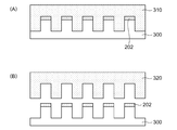
続いて、図5(A)に示すように、元型300の上にモールド材310を塗布する。モールド材310として、たとえば、ポリジメチルシロキサン(PDMS)が用いられる。塗布後のモールド材310の厚さは、例えば、0.5mmである。
続いて、図5(A)に示すように、元型300の上にモールド材310を塗布する。モールド材310として、たとえば、ポリジメチルシロキサン(PDMS)が用いられる。塗布後のモールド材310の厚さは、例えば、0.5mmである。
次に、図5(B)に示すように、モールド材310を熱硬化後、元型300から剥離して、ソフトモールド320を作製する。
<誘電体の形成>
一方、図6(A)に示すように、量子構造層の裏面側に設けられた基板90の裏面に誘電材料としてUV硬化樹脂330を塗布する。UV硬化樹脂330の厚さは、例えば、600nmである。
一方、図6(A)に示すように、量子構造層の裏面側に設けられた基板90の裏面に誘電材料としてUV硬化樹脂330を塗布する。UV硬化樹脂330の厚さは、例えば、600nmである。
次に、図6(B)に示すように、UV硬化樹脂330の上からソフトモールド320を押し付ける。ソフトモールド320押圧時の圧力は、例えば、3kPaである。
次に、図6(C)に示すように、UV照射をした後、ソフトモールド320をUV硬化樹脂330から剥離する。
次に、図7(A)に示すように、O2アッシングにより基板90の裏面に付着した残膜を除去し、正方格子状に配列され、形状が四角形状の誘電体104を形成する。
次に、図7(B)に示すように、誘電体104の上から銀を蒸着し、金属膜102を形成する。
以上の工程により、金属膜102および誘電体104を有する光反射層100を形成することができる。
(変形例)
変形例に係る光電変換素子は、誘電体104の作製方法および形状が異なる以外は、実施の形態の光電変換素子と同様である。本変形例では、図4(C)に示すドライエッチング工程に代えて、図8(A)に示すように、二酸化ケイ素層202をマスクとし、エッチング剤としてCl2の他にArを用いる。これにより、物理作用により二酸化ケイ素層202が意図的に削り込まれ、元型300に形成される凹部の内壁面が、凹部の開口に比べて凹部の底面が狭くなるようなテーパ状となる。こうして得られた元型300を用いて、実施の形態と同様な工程を経ることで、図8(B)に示すような、ソフトモールド320が得られる。このソフトモールド320を用いて、実施の形態と同様な工程を経ることで、図8(C)に示すように、光反射層100の主表面に直交する断面における形状が基板90側を長辺とする台形状の誘電体104が形成される。
変形例に係る光電変換素子は、誘電体104の作製方法および形状が異なる以外は、実施の形態の光電変換素子と同様である。本変形例では、図4(C)に示すドライエッチング工程に代えて、図8(A)に示すように、二酸化ケイ素層202をマスクとし、エッチング剤としてCl2の他にArを用いる。これにより、物理作用により二酸化ケイ素層202が意図的に削り込まれ、元型300に形成される凹部の内壁面が、凹部の開口に比べて凹部の底面が狭くなるようなテーパ状となる。こうして得られた元型300を用いて、実施の形態と同様な工程を経ることで、図8(B)に示すような、ソフトモールド320が得られる。このソフトモールド320を用いて、実施の形態と同様な工程を経ることで、図8(C)に示すように、光反射層100の主表面に直交する断面における形状が基板90側を長辺とする台形状の誘電体104が形成される。
本変形例の誘電体104の作製方法によれば、ソフトモールド320を転写のために押圧した際のUV硬化樹脂303の変形が小さくなるため、誘電体104に型抜けが生じることを抑制し、誘電体104の転写精度を高めることができる。
以下、本発明の実施例を説明するが、これら実施例は、本発明を好適に説明するための例示に過ぎず、なんら本発明を限定するものではない。
(実施例1)
<セルの作製>
有機金属気相成長(MOVPE)法を用いて、光電変換素子(量子井戸型太陽電池)を作製した。具体的には、両面が鏡面の350μm厚さの絶縁性GaAs基板(キャリア濃度:1×107cm-3)をMOVPE装置に投入し、温度600℃、圧力10kPaで、トリメチルガリウム、トリメチルインジウム、ターシャリーブチルアルシン、ターシャリーブチルフォスフィンを原料、水素をキャリアガスに用いて結晶成長を行った。まず、第2コンタクト層としてn型のGaAs(キャリア濃度:2×1018cm-3)を1μm形成した。続いて、第2半導体層(ベース層)としてn型のGaAs(キャリア濃度:2×1018cm-3)を2.5μm成膜した。次に量子構造層として、まずi相のGaAsを0.1μm成膜し、その後、量子構造として、井戸層In0.17Ga0.83As(8.54nm)、障壁層GaAs0.78P0.22(18.1nm)からなる層を20層積層した。さらに、i相のGaAsを0.1μm成膜した。この後、第1半導体層(エミッタ層)としてp型のGaAs(キャリア濃度:2×1018cm-3)を0.8μm、窓層としてp型のIn0.49Ga0.51P(キャリア濃度:5×1018cm-3)を0.04μm、第1コンタクト層(表面コンタクト層)としてp型のGaAs(キャリア濃度:1×1019cm-3)を0.04μm、順次成長させた。次に成長させたエピタキシャル層を、量子井戸層部分をマスクして第2半導体層までエッチング除去し、第2電極としてAuGe/Niを蒸着し、窒素中380℃で熱処理を施した。さらに第1コンタクト層に電極パターンの窓明けをしたレジストを形成し、Ag/Auを蒸着後、リフトオフ法にて第1電極(表面電極)を形成し、第1電極をマスクとして電極が形成されていない部分の第1コンタクト層をエッチングにより除去した。
<セルの作製>
有機金属気相成長(MOVPE)法を用いて、光電変換素子(量子井戸型太陽電池)を作製した。具体的には、両面が鏡面の350μm厚さの絶縁性GaAs基板(キャリア濃度:1×107cm-3)をMOVPE装置に投入し、温度600℃、圧力10kPaで、トリメチルガリウム、トリメチルインジウム、ターシャリーブチルアルシン、ターシャリーブチルフォスフィンを原料、水素をキャリアガスに用いて結晶成長を行った。まず、第2コンタクト層としてn型のGaAs(キャリア濃度:2×1018cm-3)を1μm形成した。続いて、第2半導体層(ベース層)としてn型のGaAs(キャリア濃度:2×1018cm-3)を2.5μm成膜した。次に量子構造層として、まずi相のGaAsを0.1μm成膜し、その後、量子構造として、井戸層In0.17Ga0.83As(8.54nm)、障壁層GaAs0.78P0.22(18.1nm)からなる層を20層積層した。さらに、i相のGaAsを0.1μm成膜した。この後、第1半導体層(エミッタ層)としてp型のGaAs(キャリア濃度:2×1018cm-3)を0.8μm、窓層としてp型のIn0.49Ga0.51P(キャリア濃度:5×1018cm-3)を0.04μm、第1コンタクト層(表面コンタクト層)としてp型のGaAs(キャリア濃度:1×1019cm-3)を0.04μm、順次成長させた。次に成長させたエピタキシャル層を、量子井戸層部分をマスクして第2半導体層までエッチング除去し、第2電極としてAuGe/Niを蒸着し、窒素中380℃で熱処理を施した。さらに第1コンタクト層に電極パターンの窓明けをしたレジストを形成し、Ag/Auを蒸着後、リフトオフ法にて第1電極(表面電極)を形成し、第1電極をマスクとして電極が形成されていない部分の第1コンタクト層をエッチングにより除去した。
<光反射層の作製>
絶縁性GaAs基板の受光面とは反対側に、上述した光反射層の作製方法に従い、表1に示す材料および厚さの金属膜と、表1に示す配置および寸法の誘電体を有する光反射層を形成した。
絶縁性GaAs基板の受光面とは反対側に、上述した光反射層の作製方法に従い、表1に示す材料および厚さの金属膜と、表1に示す配置および寸法の誘電体を有する光反射層を形成した。
(実施例2~4、比較例1~9)
実施例2~4、比較例1~9の各光電変換素子は、表1に示す諸条件を除き、上述した実施例1の光電変換素子と同様に作製した。
実施例2~4、比較例1~9の各光電変換素子は、表1に示す諸条件を除き、上述した実施例1の光電変換素子と同様に作製した。
(太陽電池性能の測定)
実施例1~4、比較例1~9の各光電変換素子について分光感度測定を行った。分光感度測定装置はキセノンランプとハロゲンランプの二灯式で、モノクロメーターで分光した300~1100nmの単色光を太陽電池に照射しACモードで行い、それぞれの波長の照射光子数と光電流値から量子収率を算出した。また、絶縁性GaAs基板の裏面に光反射層を設けない、基準となる光電変換素子についても同様に量子収率を算出した。実施例1~4、比較例1~9の各光電変換素子の量子構造層に起因する波長範囲(900~1100nm)の量子収率が基準となる光電変換素子に対して何倍になるかを算出し、効果として表1に記載した。
実施例1~4、比較例1~9の各光電変換素子について分光感度測定を行った。分光感度測定装置はキセノンランプとハロゲンランプの二灯式で、モノクロメーターで分光した300~1100nmの単色光を太陽電池に照射しACモードで行い、それぞれの波長の照射光子数と光電流値から量子収率を算出した。また、絶縁性GaAs基板の裏面に光反射層を設けない、基準となる光電変換素子についても同様に量子収率を算出した。実施例1~4、比較例1~9の各光電変換素子の量子構造層に起因する波長範囲(900~1100nm)の量子収率が基準となる光電変換素子に対して何倍になるかを算出し、効果として表1に記載した。
表1の結果が示すように、実施例1~4の各光電変換素子は、比較例1~9の各光電変換素子に比べて量子収率の向上効果が大きいことが明らかとなった。
(誘電体占有面積依存性)
誘電体の露出部の一辺の長さDを実施例1と共通の630nmとし、隣接する誘電体の間隔Wを変化させた光電変換素子に対して、それぞれ、基準となる光電変換素子に対して量子構造層に起因する波長範囲の量子収率が何倍になるか算出した。図9に、光反射層の主表面全体に対して誘電体の露出部の総面積が占める割合と、量子収率の向上効果との関係を示す。図9より、光反射層の主表面全体に対して前記誘電体の露出部の総面積が占める割合が0.4~0.8のときに量子収率の向上効果が顕著に大きいことが確認された。
誘電体の露出部の一辺の長さDを実施例1と共通の630nmとし、隣接する誘電体の間隔Wを変化させた光電変換素子に対して、それぞれ、基準となる光電変換素子に対して量子構造層に起因する波長範囲の量子収率が何倍になるか算出した。図9に、光反射層の主表面全体に対して誘電体の露出部の総面積が占める割合と、量子収率の向上効果との関係を示す。図9より、光反射層の主表面全体に対して前記誘電体の露出部の総面積が占める割合が0.4~0.8のときに量子収率の向上効果が顕著に大きいことが確認された。
本発明は、上述の各実施の形態に限定されるものではなく、当業者の知識に基づいて各種の設計変更等の変形を加えることも可能であり、そのような変形が加えられた実施の形態も本発明の範囲に含まれうるものである。
誘電体104の露出部の形状が「四角形状」という用語については、角部が90°の形状であることに限定されず、図10のように、光反射層を平面視したときに、誘電体104の角部が丸みを帯びた形状となる場合も含まれる。ただし、誘電体104の一辺の長さDと、丸みを帯びた部分の当該一辺の長さ方向の幅rとの比、D:rは、1:0~1:0.2の範囲とする。
10 光電変換素子、20 第1電極、30 第1コンタクト層、40 窓層、50 第1半導体層、60 量子構造層、70 第2半導体層、80 第2コンタクト層、90 基板、100 光反射層、102 金属膜、104 誘電体、110 第2電極
本発明は、光電変換素子および光電変換素子の作製方法に利用することができる。
Claims (7)
- 光電変換層と、
前記光電変換層の受光面側とは反対側に設けられている金属膜と、前記金属膜の前記光電変換層の側の主表面に設けられた複数の凹部にそれぞれ充填された誘電体と、を有する光反射層と、
を備え、
前記光電変換層と対向する前記光反射層の主表面を平面視したときに前記誘電体の露出部が四角形状であり、
前記光電変換層と対向する前記光反射層の主表面を平面視したときに複数の前記誘電体が正方格子状に配列されていることを特徴とする光電変換素子。 - 前記光電変換層と前記光反射層との間に基板が設けられ、
前記基板の裏面に前記金属膜および前記誘電体が接している請求項1に記載の光電変換素子。 - 前記光電変換層が、受光面側に位置する第1の半導体層と、
前記第1の半導体層の導電型と反対の導電型の第2の半導体層と、
前記第1の半導体層と前記第2の半導体層との間に設けられており、前記第1の半導体層および前記第2の半導体層のバンドギャップ以上のバンドギャップを有する1以上の第1の半導体領域と、前記第1の半導体層及び前記第2の半導体層のバンドギャップ以下のバンドギャップを有する1以上の第2の半導体領域と、を有する量子構造層と、
から構成されている請求項1または2に記載の光電変換素子。 - 前記誘電体の露出部の1辺の長さと、隣接する誘電体の間隔の和が600nm~1000nmである請求項1乃至3のいずれか1項に記載の光電変換素子。
- 前記光電変換層と対向する前記光反射層の主表面を平面視したときに、前記光反射層の主表面全体に対して前記誘電体の露出部の総面積が占める割合が0.4~0.8である請求項1乃至4のいずれか1項に記載の光電変換素子。
- 前記光反射層の主表面と直交する断面における前記誘電体の形状が、前記光電変換層側を長辺とする台形状である請求項1乃至5のいずれか1項に記載の光電変換素子。
- 光電変換層の受光面側とは反対側に誘電材料を塗布する工程と、
前記誘電材料の上から正方格子状に凹部が配列されたパターンを有するモールドを押圧して、前記光電変換層の受光面側とは反対側に複数の誘電体を形成する工程と、
前記複数の誘電体の上から金属を蒸着する工程と、
を備え、
前記凹部の内壁面が、前記凹部の開口に比べて凹部の底面が狭くなるようなテーパ状であることを特徴とする光電変換素子の作製方法。
Applications Claiming Priority (2)
| Application Number | Priority Date | Filing Date | Title |
|---|---|---|---|
| JP2013-124780 | 2013-06-13 | ||
| JP2013124780A JP2015002203A (ja) | 2013-06-13 | 2013-06-13 | 光電変換素子および光電変換素子の作製方法 |
Publications (1)
| Publication Number | Publication Date |
|---|---|
| WO2014199573A1 true WO2014199573A1 (ja) | 2014-12-18 |
Family
ID=52021894
Family Applications (1)
| Application Number | Title | Priority Date | Filing Date |
|---|---|---|---|
| PCT/JP2014/002719 Ceased WO2014199573A1 (ja) | 2013-06-13 | 2014-05-23 | 光電変換素子および光電変換素子の作製方法 |
Country Status (2)
| Country | Link |
|---|---|
| JP (1) | JP2015002203A (ja) |
| WO (1) | WO2014199573A1 (ja) |
Citations (4)
| Publication number | Priority date | Publication date | Assignee | Title |
|---|---|---|---|---|
| JPH05505911A (ja) * | 1991-02-04 | 1993-08-26 | パウル・シエーレル・インステイトウト | 太陽電池 |
| JPH11220150A (ja) * | 1998-02-02 | 1999-08-10 | Hitachi Ltd | 太陽電池 |
| WO2012169123A1 (ja) * | 2011-06-10 | 2012-12-13 | Jx日鉱日石エネルギー株式会社 | 光電変換素子 |
| JP2013219073A (ja) * | 2012-04-04 | 2013-10-24 | Jx Nippon Oil & Energy Corp | 光電変換素子 |
-
2013
- 2013-06-13 JP JP2013124780A patent/JP2015002203A/ja active Pending
-
2014
- 2014-05-23 WO PCT/JP2014/002719 patent/WO2014199573A1/ja not_active Ceased
Patent Citations (4)
| Publication number | Priority date | Publication date | Assignee | Title |
|---|---|---|---|---|
| JPH05505911A (ja) * | 1991-02-04 | 1993-08-26 | パウル・シエーレル・インステイトウト | 太陽電池 |
| JPH11220150A (ja) * | 1998-02-02 | 1999-08-10 | Hitachi Ltd | 太陽電池 |
| WO2012169123A1 (ja) * | 2011-06-10 | 2012-12-13 | Jx日鉱日石エネルギー株式会社 | 光電変換素子 |
| JP2013219073A (ja) * | 2012-04-04 | 2013-10-24 | Jx Nippon Oil & Energy Corp | 光電変換素子 |
Also Published As
| Publication number | Publication date |
|---|---|
| JP2015002203A (ja) | 2015-01-05 |
Similar Documents
| Publication | Publication Date | Title |
|---|---|---|
| CN106159008B (zh) | 太阳能电池及其制造方法 | |
| US8410353B2 (en) | Asymmetric surface texturing for use in a photovoltaic cell and method of making | |
| Liu et al. | Optoelectronic devices based on the integration of halide perovskites with silicon-based materials | |
| US20100012969A1 (en) | Light emitting device and fabrication method thereof | |
| US9117967B2 (en) | Method of manufacturing glass substrate with concave-convex film using dry etching, glass substrate with concave-convex film, solar cell, and method of manufacturing solar cell | |
| JP2009246025A (ja) | 太陽電池およびその製造方法 | |
| TW200423421A (en) | Improved LED efficiency using photonic crystal structure | |
| CN111725338B (zh) | 一种微米线阵列异质结紫外光探测器及其制备方法 | |
| US10957808B2 (en) | Flexible double-junction solar cell | |
| TWI518925B (zh) | A photovoltaic element device having a surface periodic grating structure and a method of manufacturing the same | |
| CN105070779A (zh) | 具有亚波长光栅结构的面入射硅基锗光电探测器及其制备方法 | |
| US20230253439A1 (en) | Semiconductor device and method of fabricating the same | |
| JPH09260710A (ja) | 半導体装置 | |
| US20140090705A1 (en) | Photoelectric conversion element | |
| WO2020156239A1 (zh) | 光电二极管及其制备方法、电子设备 | |
| TWI483410B (zh) | 太陽能電池、其製造方法及其模組 | |
| WO2012160764A1 (ja) | 光電変換素子 | |
| US20160005892A1 (en) | Vertical pillar structure photovoltaic devices and method for making the same | |
| JP5900400B2 (ja) | Iii族窒化物半導体発光素子の製造方法 | |
| KR101266337B1 (ko) | 실리콘 태양전지의 제조방법 | |
| JP2005277181A (ja) | 半導体装置の製造方法 | |
| CN116469944A (zh) | 一种ii类超晶格光电探测器及其制作方法 | |
| JP2015002203A (ja) | 光電変換素子および光電変換素子の作製方法 | |
| JP2013219073A (ja) | 光電変換素子 | |
| JP2012009554A (ja) | 光電変換素子 |
Legal Events
| Date | Code | Title | Description |
|---|---|---|---|
| 121 | Ep: the epo has been informed by wipo that ep was designated in this application |
Ref document number: 14810826 Country of ref document: EP Kind code of ref document: A1 |
|
| NENP | Non-entry into the national phase |
Ref country code: DE |
|
| 122 | Ep: pct application non-entry in european phase |
Ref document number: 14810826 Country of ref document: EP Kind code of ref document: A1 |