WO2014196262A1 - イオン源およびイオンミリング装置 - Google Patents
イオン源およびイオンミリング装置 Download PDFInfo
- Publication number
- WO2014196262A1 WO2014196262A1 PCT/JP2014/060102 JP2014060102W WO2014196262A1 WO 2014196262 A1 WO2014196262 A1 WO 2014196262A1 JP 2014060102 W JP2014060102 W JP 2014060102W WO 2014196262 A1 WO2014196262 A1 WO 2014196262A1
- Authority
- WO
- WIPO (PCT)
- Prior art keywords
- cathode
- chamber
- ion
- ion source
- region
- Prior art date
- Legal status (The legal status is an assumption and is not a legal conclusion. Google has not performed a legal analysis and makes no representation as to the accuracy of the status listed.)
- Ceased
Links
Images










Classifications
-
- H—ELECTRICITY
- H01—ELECTRIC ELEMENTS
- H01J—ELECTRIC DISCHARGE TUBES OR DISCHARGE LAMPS
- H01J27/00—Ion beam tubes
- H01J27/02—Ion sources; Ion guns
- H01J27/08—Ion sources; Ion guns using arc discharge
- H01J27/14—Other arc discharge ion sources using an applied magnetic field
- H01J27/146—End-Hall type ion sources, wherein the magnetic field confines the electrons in a central cylinder
-
- H—ELECTRICITY
- H01—ELECTRIC ELEMENTS
- H01J—ELECTRIC DISCHARGE TUBES OR DISCHARGE LAMPS
- H01J37/00—Discharge tubes with provision for introducing objects or material to be exposed to the discharge, e.g. for the purpose of examination or processing thereof
- H01J37/02—Details
- H01J37/04—Arrangements of electrodes and associated parts for generating or controlling the discharge, e.g. electron-optical arrangement or ion-optical arrangement
- H01J37/08—Ion sources; Ion guns
-
- H—ELECTRICITY
- H01—ELECTRIC ELEMENTS
- H01J—ELECTRIC DISCHARGE TUBES OR DISCHARGE LAMPS
- H01J2237/00—Discharge tubes exposing object to beam, e.g. for analysis treatment, etching, imaging
- H01J2237/02—Details
- H01J2237/022—Avoiding or removing foreign or contaminating particles, debris or deposits on sample or tube
-
- H—ELECTRICITY
- H01—ELECTRIC ELEMENTS
- H01J—ELECTRIC DISCHARGE TUBES OR DISCHARGE LAMPS
- H01J2237/00—Discharge tubes exposing object to beam, e.g. for analysis treatment, etching, imaging
- H01J2237/06—Sources
- H01J2237/08—Ion sources
- H01J2237/0815—Methods of ionisation
- H01J2237/082—Electron beam
Definitions
- the present invention relates to an ion source and an ion milling apparatus.
- the ion milling method is a processing method in which a sample is scraped using a sputtering phenomenon in which accelerated ions collide with a sample and the ions repel atoms and molecules.
- the sample is irradiated with an ion beam with a mask serving as an ion beam shielding plate placed on the upper surface of the sample, and the portion of the sample protruding from the end of the mask is sputtered by ions.
- a smooth cross section can be processed.
- a sample made of metal, glass, ceramics, an electronic component, a composite material, or the like can be processed.
- morphological images, sample composition images, or channeling images with a scanning electron microscope for the purpose of evaluating the internal structure, cross-sectional shape or film thickness, or analyzing the crystal state, failure, or cross-section of foreign matter
- X-ray analysis or crystal orientation analysis an ion milling method is used.
- a Penning ion gun is used as an ion source.
- the Penning ion gun includes a gas supply mechanism, an anode, a cathode, and a permanent magnet.
- a Penning type ion gun in order to easily start discharge and to maintain the discharge stably, many electrons must be emitted from the cathode.
- Patent Document 1 discloses the structure of such a Penning ion gun.
- Patent Document 2 describes an ion gun structure in which the surface of the cathode constituting the ion gun is formed of a nonmagnetic material having conductivity, that is, a nonmagnetic material. .
- the non-magnetic particles sputtered by the collision of cations generated inside the ion gun are deposited on the inner surface of the anode, but are deposited on the anode like a conventional needle. It is disclosed that abnormal discharge can be prevented.
- Patent Document 3 discloses that in an arc discharge apparatus, a lattice-shaped groove is formed on the surface of a liner base provided inside a chamber to regulate the size of unnecessary deposits. Thus, a method for preventing poor insulation between the liner base and the electrode is described.
- argon ions which are cations generated in the ionization chamber, are accelerated toward the cathode inside the ion gun, and collide with a region of the cathode surface facing the inside of the ionization chamber. Due to the collision of ions, the surface of the cathode is sputtered, and the particles sputtered from the cathode surface, that is, most of the sputtered particles are deposited on the surface of the anode.
- the cathode is made of a magnetic conductor such as pure iron
- the sputtered particles are also made of a magnetic conductor. Therefore, the deposited film in which the sputtered particles are deposited on the surface of the anode follows the direction of the magnetic field generated by the permanent magnet. It grows like a needle.
- a discharge voltage is applied between the cathode and the anode by a discharge power source. Therefore, abnormal discharge occurs between the cathode and the anode via a deposited film in which sputtered particles are deposited on the anode.
- a power supply circuit that applies a voltage between the cathode and the anode is short-circuited due to abnormal discharge, and a predetermined voltage is not applied between the cathode and the anode.
- the amount of electrons emitted from the cathode decreases or becomes zero as the accumulated time of ion milling increases, resulting in the phenomenon that the ion beam is not emitted from the ion gun. To do. That is, as the milling integration time increases, abnormal discharge tends to occur inside the ion gun, and the ion gun cannot be operated normally for a long time.
- the cathode has a main body portion and a non-conductive electrode disposed on the surface of the main body portion. It may include a magnetic material, that is, a nonmagnetic portion made of a nonmagnetic conductor.
- the non-magnetic part is made of, for example, titanium as a non-magnetic conductor, the particles emitted from the surface of the non-magnetic part are sputtered by colliding with some of the cations generated in the ionization chamber. TiOx as a main component.
- TiOx is made of an electrically insulating material, that is, an insulator, the surface of the anode is covered with an insulating film formed by depositing TiOx, so that the function as the anode electrode is lowered and the ion gun is lengthened. It cannot operate normally over time.
- the present invention provides an ion source and an ion milling device that can be operated normally for a long time without causing abnormal discharge inside an ion gun as an ion source.
- An ion source includes a first chamber and an ion generator that ionizes gas in the first chamber to generate ions.
- the ion generation unit includes an anode provided in the first chamber, a first cathode that is provided facing the first chamber and emits electrons, a gas supply unit that supplies gas to the first chamber, and a first chamber And a magnetic field generator for generating a magnetic field.
- the ion generation unit generates ions in the first chamber by causing electrons emitted from the first cathode to rotate by the magnetic field generated by the magnetic field generation unit and collide with the gas supplied by the gas supply unit. It is. And the unevenness
- an ion milling apparatus includes a first chamber provided in an airtight manner, a vacuum exhaust unit that evacuates the first chamber, a sample holding unit that holds a sample in the first chamber, and a sample An ion source for injecting ions toward the sample held by the holding unit to process the sample.
- the ion source includes a second chamber, a hole formed in the second chamber, an ion generation unit that ionizes gas in the second chamber to generate ions, and ions generated in the second chamber. Through the second chamber, and the second chamber communicates with the first chamber through the hole.
- the ion generation unit includes an anode provided in the second chamber, a first cathode that is provided facing the second chamber and emits electrons, a gas supply unit that supplies gas to the second chamber, and a second chamber And a magnetic field generator for generating a magnetic field.
- the ion generator generates ions in the second chamber by causing electrons emitted from the first cathode to rotate by the magnetic field generated by the magnetic field generator and collide with the gas supplied by the gas supply unit. It is. Unevenness is formed in the first region facing the second chamber on the surface of the first cathode.
- an ion source and an ion milling apparatus can be operated normally for a long time without causing abnormal discharge inside an ion gun as an ion source.
- FIG. 1 is an overall configuration diagram of an ion milling apparatus according to Embodiment 1.
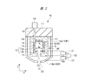
- FIG. 1 is a cross-sectional view showing a configuration of an ion gun according to Embodiment 1.
- FIG. 3 is a plan view showing a cathode in Embodiment 1.
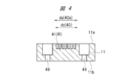
- FIG. 3 is a cross-sectional view showing the cathode in the first embodiment.
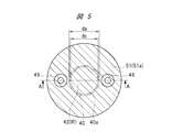
- 6 is a plan view showing a cathode in a first modification of the first embodiment.
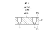
- FIG. FIG. 7 is a cross-sectional view showing a cathode in a first modification of the first embodiment. 6 is a plan view showing a cathode in a second modification of the first embodiment.
- FIG. 1 is an overall configuration diagram of an ion milling apparatus according to Embodiment 1.
- FIG. 1 is a cross-sectional view showing a configuration of an ion gun according to Embodiment 1.
- FIG. 3 is a plan view showing a cathode in Em
- FIG. 6 is a cross-sectional view showing a cathode in a second modification of the first embodiment.
- FIG. It is sectional drawing which shows the structure of the ion gun of the comparative example 1. It is sectional drawing which shows the structure of the ion gun of the comparative example 2. It is a graph which shows an example of the relationship between the milling integration time in the ion gun of the comparative example 1 and the comparative example 2, and the variation
- FIG. 4 is a plan view showing a cathode in a second embodiment.
- 6 is a cross-sectional view showing a main body portion of a cathode according to Embodiment 2.
- FIG. FIG. 4 is a plan view showing a cathode in a second embodiment.
- 6 is a cross-sectional view showing a main body portion of a cathode according to Embodiment 2.
- FIG. 5 is a cross-sectional view showing a cathode mounting portion in a second embodiment.
- 6 is a plan view showing a cathode in a first modification of the second embodiment.
- FIG. 6 is a cross-sectional view showing a main body portion of a cathode in a first modification of the second embodiment.
- FIG. 10 is a cross-sectional view showing a cathode mounting portion in a first modification of the second embodiment.
- FIG. 10 is a plan view showing a cathode in a third embodiment.
- FIG. 4 is a cross-sectional view showing a cathode in a third embodiment.
- the constituent elements are not necessarily indispensable unless otherwise specified and apparently essential in principle. Needless to say.
- the shapes, positional relationships, etc. of the components, etc. when referring to the shapes, positional relationships, etc. of the components, etc., the shapes are substantially the same unless otherwise specified, or otherwise apparent in principle. And the like are included. The same applies to the above numerical values and ranges.
- hatching may be omitted even in a cross-sectional view for easy viewing of the drawings. Further, even a plan view may be hatched to make the drawing easy to see.
- the ion source is described as an example when applied to an ion source of an ion milling apparatus as an ion beam processing apparatus.
- the ion source of each embodiment is not limited to an ion milling apparatus, but is also a SIM (Scanning Ion Microscope) or ion beam that irradiates a sample with an ion beam and detects secondary electrons and reflected electrons generated secondaryly.
- SIM Single Imaging Ion Microscope
- the present invention can be applied to other various ion beam irradiation apparatuses such as an ion microscope.
- the embodiments described below can be combined as appropriate without departing from the scope of the present invention.
- FIG. 1 is an overall configuration diagram of the ion milling apparatus according to the first embodiment.
- the ion milling apparatus has a vacuum chamber VC, a vacuum exhaust system VP, a sample holding part SP, and an ion gun IG.
- the vacuum chamber VC is provided in an airtight manner and is a processing chamber in which a sample is milled, that is, processed.
- the evacuation system VP is a evacuation unit that evacuates the inside of the vacuum chamber VC.
- the pressure inside the vacuum chamber VC is controlled to atmospheric pressure or vacuum by the evacuation system VP.
- the sample holder SP holds the sample 6 inside the vacuum chamber VC.
- the sample holder SP includes a sample stage 7, a sample stage 8, and a sample stage drive unit 9.
- the sample 6 is held on a sample stage 7, and the sample stage 7 is held on a sample stage 8.
- the sample stage 8 is configured so that it can be pulled out of the vacuum chamber VC when the vacuum chamber VC is opened to the atmosphere, and the sample 6 is inclined at an arbitrary angle with respect to the optical axis of the ion beam IB. It is comprised so that it can be made to.
- the sample stage drive unit 9 can swing the sample stage 8 left and right, and can control the speed thereof.
- the ion gun IG generates ions inside the ion gun IG, injects the generated ions toward the sample 6 held in the sample holding unit SP, and irradiates the sample 6 with an ion beam IB composed of the emitted ions. And an ion source for processing the sample 6.
- the irradiation of the ion beam IB and its current density are controlled by the ion gun controller GC.
- FIG. 2 is a cross-sectional view showing the configuration of the ion gun of the first embodiment.
- the ion gun IG has an ionization chamber IC, an ion generation part GP, and an ion ejection part IP.
- the ion generator GP generates ions by ionizing a gas in the ionization chamber IC.
- the ion ejection unit IP ejects ions generated in the ionization chamber IC from the ionization chamber IC through a hole formed in the ionization chamber IC.
- the ion gun IG includes a gas supply mechanism 10, a cathode 11, a cathode 12, an anode 13, a permanent magnet 14, an acceleration electrode 15, an insulator 16, and a base 17.
- the ion gun IG includes a discharge power source 21 and an acceleration power source 22.
- the gas supply mechanism 10, the cathode 11, the cathode 12, the anode 13, and the permanent magnet 14 constitute an ion generation part GP.
- the acceleration electrode 15 constitutes the ion ejection part IP.
- the gas supply mechanism 10 is a gas supply unit that supplies gas to the ionization chamber IC.
- the cathode 11 is provided facing the inside of the ionization chamber IC, and a negative voltage is applied to the anode 13 to emit electrons.
- the cathode 12 is provided facing the inside of the ionization chamber IC, and a negative voltage is applied to the anode 13 to emit electrons.
- the anode 13 is provided inside the ionization chamber IC, and a positive voltage is applied to the cathode 11 and the cathode 12.
- the permanent magnet 14 is a magnetic field generator that generates a magnetic field inside the ionization chamber IC.
- the cathode 11, the cathode 12, the anode 13, the permanent magnet 14, the acceleration electrode 15, and the insulator 16 are fixed to the base 17.
- the cathode 11 is made of a conductive magnetic material such as pure iron and is formed in a disk shape. That is, the cathode 11 is made of a magnetic conductor and is formed in a disk shape.
- the cathode 11 is fixed to the base 17 by, for example, screwing.
- a hole 18 that penetrates the cathode 11 is formed in the cathode 11.
- the hole 18 is for introducing a gas such as argon gas into the ionization chamber IC.
- the shape of the cathode 11 is not limited to a disk shape. Therefore, the cathode 11 may be formed in a plate shape.
- the unevenness IR is formed in the region 40 facing the inside of the ionization chamber IC on the surface of the cathode 11.
- the specific structure of the cathode 11 will be described later.
- the cathode 12 is made of a conductive magnetic material such as pure iron and is formed in a disk shape. That is, the cathode 12 is made of a magnetic conductor and is formed in a disk shape. An ion beam passage hole 31 for allowing the ion beam to pass therethrough is formed at the center of the cathode 12. Further, the shape of the cathode 12 is not limited to a disk shape. Therefore, the cathode 12 may be formed in a plate shape.
- the permanent magnet 14 is made of a ferromagnetic material having conductivity including a ferromagnetic metal such as a neodymium magnet, and is formed in a cylindrical shape extending in the Z-axis direction in FIG.
- the cathode 11 is attracted to one end in the Z-axis direction of the permanent magnet 14, that is, one end portion by a magnetic force, and one end of the permanent magnet 14 is connected to the cathode 11.
- the cathode 12 is attracted to the other end of the permanent magnet 14 in the Z-axis direction, that is, the other end by a magnetic force, and the cathode 12 is connected to the other end of the permanent magnet 14. Since the cathode 11, the cathode 12 and the permanent magnet 14 are electrically connected to each other, the cathode 11, the cathode 12 and the permanent magnet 14 are kept at the same potential.
- the ionization chamber IC is partitioned by the permanent magnet 14, the cathode 11 and the cathode 12, and the ion beam passage hole 31 is a hole formed in the ionization chamber IC.
- the permanent magnet 14 generates a magnetic field inside the ionization chamber IC.
- the cathode 11 and the cathode 12 form a magnetic path, the magnetic field generated in the ionization chamber IC can be strengthened by the cathode 11 and the cathode 12.
- the shape of the permanent magnet 14 is not limited to a cylindrical shape. Therefore, the permanent magnet 14 may be formed in a cylindrical shape.
- the insulator 16 is formed in a cylindrical shape extending in the Z-axis direction in FIG.
- the insulator 16 is disposed inside the permanent magnet 14, and the outer peripheral surface of the insulator 16 is in contact with the inner peripheral surface of the permanent magnet 14.
- the insulator 16 is made of a nonmagnetic material having electrical insulating properties such as ceramics.
- the anode 13 includes a cylindrical portion 13a and a bottom portion 13b, and is made of a nonmagnetic material having conductivity, such as aluminum. That is, the anode 13 is made of a nonmagnetic conductor.
- the cylindrical portion 13 a is formed in a cylindrical shape that extends in the Z-axis direction of FIG. 2 and is fitted inside the insulator 16.
- the outer peripheral surface of the cylindrical part 13a is in contact with the inner peripheral surface of the insulator 16, and the inner peripheral surface of the cylindrical part 13a faces the inside of the ionization chamber IC.
- the bottom portion 13b is formed on the side opposite to the base 17 of the cylindrical portion 13a, and an ion beam passage hole 32 is provided in the central portion of the bottom portion 13b.
- the anode 13 is electrically insulated from the cathode 11, the cathode 12 and the permanent magnet 14 by an insulator 16. Further, the shape of the anode 13 is not limited to a cylindrical shape. Therefore, the anode 13 may be formed in a cylindrical shape.
- the acceleration electrode 15 is provided on the opposite side to the inside of the ionization chamber IC with the ion beam passage hole 31 in between.
- the acceleration electrode 15 includes a cylindrical portion 15a and a bottom portion 15b, and is made of a nonmagnetic material having conductivity, such as stainless steel.
- the cylindrical portion 15 a extends in the Z-axis direction of FIG. 2 and is formed in a cylindrical shape surrounding the ionization chamber IC, and one end portion in the Z-axis direction is fixed to the base 17.
- the bottom portion 15b is formed on the side opposite to the base 17 of the cylindrical portion 15a, and an ion beam passage hole 33 is provided in the central portion of the bottom portion 15b.
- the acceleration electrode 15 is fixed to the periphery of the base 17 so as to surround the cathode 11, the cathode 12, and the permanent magnet 14, and is maintained at the ground potential. Further, the shape of the acceleration electrode 15 is not limited to a cylindrical shape. Therefore, the acceleration electrode 15 may be formed in a cylindrical shape.
- the ionization chamber IC is connected to a vacuum chamber VC (see FIG. 1) as a processing chamber via an ion beam passage hole 31 formed in the cathode 12 and an ion beam passage hole 33 formed in the acceleration electrode 15. Communicate.
- the base 17 is formed with a hole 19 that penetrates the base 17 and communicates with a hole 18 that penetrates the cathode 11.
- the gas supply mechanism 10 is connected to the base 17 so that gas can be introduced into the ionization chamber IC through the holes 19 and 18.
- the gas supply mechanism 10 adjusts the flow rate of the gas supplied to the ionization chamber IC.
- One terminal of the discharge power source 21 is electrically connected to the cathode 11 and the cathode 12, and the other terminal of the discharge power source 21 is electrically connected to the anode 13, and the cathode 11 and the cathode 12, A discharge voltage is applied between the anode 13 and the discharge power source 21.
- One terminal of the acceleration power source 22 is electrically connected to the cathode 11 and the cathode 12, and the other terminal of the acceleration power source 22 is electrically connected to the acceleration electrode 15. An acceleration voltage is applied between the acceleration electrode 15 and the acceleration electrode 15 by the acceleration power source 22.
- the discharge power source 21 and the acceleration power source 22 are connected to the ion gun control unit GC, and the ion gun control unit GC controls the discharge voltage of the discharge power source 21 and the acceleration voltage of the acceleration power source 22.
- the gas to be ionized is argon gas
- the gas ionized by the ion source of the first embodiment is not limited to argon gas.
- the holes 17 and 18 are formed in the base 17 and the cathode 11, and the argon gas from the gas supply mechanism 10 is supplied to the ionization chamber IC through the holes 19 and 18.
- a negative voltage is applied to the cathode 11 and the cathode 12 with respect to the anode 13.
- a discharge voltage of about 0 to 4 kV is applied between the cathode 12 and the anode 13 by the discharge power source 21.
- the electrons emitted from the cathode 11 are rotated by the magnetic field generated by the permanent magnet 14, that is, swung to collide with the gas supplied by the gas supply mechanism 10.
- Glow discharge is performed in the ionization chamber IC to generate argon ions that are positive ions.
- the cathode 11, the cathode 12, and the acceleration electrode are applied so that a negative voltage is applied to the acceleration electrode 15 with respect to the cathode 11 and the cathode 12 in a state where argon ions that are positive ions are generated in the ionization chamber IC.
- an acceleration voltage of about 0 to 10 kV is applied by the acceleration power source 22.
- argon ions which are positive ions generated in the ionization chamber IC, are ejected from the inside of the ionization chamber IC to the outside of the ionization chamber IC, that is, the inside of the vacuum chamber VC (see FIG. 1).
- the sample 6 is irradiated with the ion beam IB which consists of a cation, and the sample 6 is processed.
- argon ions which are positive ions generated in the ionization chamber IC
- a part of argon ions is accelerated toward the cathode 11 facing the inside of the ionization chamber IC, and a region of the surface of the cathode 11 facing the inside of the ionization chamber IC.
- the unevenness IR is formed in the region 40 facing the inside of the ionization chamber IC on the surface of the cathode 11.
- the irradiation angle at which the cations are irradiated on the bottom of the irregularities IR is limited to a narrow range centering on the direction perpendicular to the surface of the cathode 11, thereby reducing the sputtering yield.
- the sputtered particles emitted from the bottom of the unevenness IR are reattached inside the unevenness IR. Furthermore, the sputtered particles emitted from the unevenness IR are scattered.
- the amount of sputtered particles deposited on the inner peripheral surface of the anode 13 can be reduced. Therefore, the ion gun and the ion milling apparatus can be operated normally for a long time without causing abnormal discharge in the ion gun.
- FIG. 3 is a plan view showing the cathode in the first embodiment
- FIG. 4 is a cross-sectional view showing the cathode in the first embodiment. 4 is a cross-sectional view taken along line AA in FIG.
- the cathode 11 has a front surface 11a and a back surface 11b, and is formed in a disc shape.
- the cathode 11 has a screw fixing hole 49 for fixing the cathode 11 to the base 17 with a screw.
- the cathode 11 is made of a conductive magnetic material, that is, a magnetic conductor.
- the unevenness IR formed in the region 40 facing the inside of the ionization chamber IC in the surface 11a of the cathode 11 is in the region 40 facing the inside of the ionization chamber IC in the surface 11a of the cathode 11. It consists of holes 41 as a plurality of formed holes.
- the depth of each of the plurality of holes 41 is preferably 1 mm or more.
- the depth of the hole 41 is less than 1 mm, for example, when the cathode 11 is used for an accumulated time of about 1000 hours in a normal operation, the surface 11a of the cathode 11 may be sputtered and scraped and the hole 41 may disappear. There is.
- the depth of the hole 41 can be less than the thickness of the cathode 11.
- the unevenness IR is 0.4 mm.
- Thirty-one holes 41 having a diameter and a depth of 1 mm can be formed. The ratio of the area occupied by the holes 41 to the area of the region 40 is about 20%.
- a circular hole is formed as the hole 41 in plan view, but the hole 41 may be a circular hole as long as it forms irregularities on the surface 11 a of the cathode 11. It is not limited, and a polygonal hole may be formed in plan view. However, from the viewpoint that it can be easily manufactured, it is preferable to form a circular hole as the hole 41 in plan view as shown in FIG.
- plan view means that the hole 41 is viewed from a direction perpendicular to the surface 11a of the cathode 11 in which the hole 41 is formed, and the direction parallel to the surface 11a of the cathode 11 is the X axis in FIG.
- the direction perpendicular to the surface 11a of the cathode 11 means the Z-axis direction in FIG.
- the region 40 is a circular region enclosed in a circular region 40a surrounded by the inner peripheral surface of the cylindrical anode 13 when viewed from the Z-axis direction (see FIG. 2). .
- the amount of collision of argon ions with the surface 11a of the cathode 11 in the region 40a, which is the region immediately above the cylindrical anode 13, is larger than the amount of collision of argon ions with the surface 11a of the cathode 11 in regions other than the region 40a. .
- the unevenness IR including the holes 41 is formed on the surface 11 a of the cathode 11, so that the sputtered particles are formed on the anode 13.
- the effect of reducing the amount deposited on the inner peripheral surface can be further increased.
- the region 40 is preferably extended by the cylindrical anode 13. When viewed from the direction, it is included in a region 40 a surrounded by the inner peripheral surface of the cylindrical anode 13.
- the diameter of the anode 13 that is, the diameter of the circular region 40a is set.
- the diameter da and the diameter dc are expressed by the following formula (1). dc ⁇ 0.7da Formula (1) Meet the conditions. Specifically, for example, when the diameter da of the region 40a is 100 mm, the diameter dc of the region 40 can be set to 70 mm or more and less than 100 mm.
- the circular region 40 that satisfies the expression (1) is the center of the circular region 40a.
- the amount of collision of argon ions with the surface 11a of the cathode 11 in the circular region 40, which is the center of the circular region 40a, is larger than the amount of collision of argon ions with the surface 11a of the cathode 11 in regions other than the region 40a. , Very many. Therefore, in the region 40 included in the region 40 a surrounded by the inner peripheral surface of the cylindrical anode 13, the unevenness IR including the holes 41 is formed on the surface 11 a of the cathode 11, so that the sputtered particles are formed on the anode 13. The effect of reducing the amount deposited on the inner peripheral surface can be further increased.
- the circular region 40 is not a region centered on the same position as the center of the circular region 40a, but is a region centered on a position near the center of the circular region 40a. By satisfying the formula (1), the same effect can be obtained.
- FIG. 5 is a plan view showing the cathode in the first modification of the first embodiment
- FIG. 6 is a cross-sectional view showing the cathode in the first modification of the first embodiment. 6 is a cross-sectional view taken along line AA in FIG.
- the cathode 51 has a front surface 51a and a back surface 51b, and is formed in a disk shape from pure iron as a conductive magnetic material.
- the cathode 51 is provided with a screw fixing hole 49 for fixing the cathode 51 to the base 17.
- the unevenness 42 in which the surface 51a of the cathode 51 is roughened is formed in the region 40 facing the inside of the ionization chamber IC in the surface 51a of the cathode 51.
- the average roughness of the irregularities 42 in which the surface 51a of the cathode 51 is roughened is 50 ⁇ m or more.
- the average roughness means the arithmetic average roughness Ra.
- the average roughness of the unevenness 42 When the average roughness of the unevenness 42 is less than 50 ⁇ m, the roughness of the unevenness 42 becomes too small, the effect of reducing the sputter yield, the effect of reattaching the sputtered particles inside the unevenness IR, and the scattering of the sputtered particles There is a risk that the effect will be reduced. Therefore, by setting the average roughness of the unevenness 42 to 50 ⁇ m or more, the effect of reducing the sputtering yield, the effect of reattaching the sputtered particles inside the unevenness IR, or the effect of scattering the sputtered particles increases. The amount of sputtered particles deposited on the inner peripheral surface of the anode 13 can be reduced.
- the region 40 is preferably surrounded by the inner peripheral surface of the cylindrical anode 13 when viewed from the Z-axis direction (see FIG. 2). This is a circular region included in the circular region 40a.
- the diameter da of the region 40a and the diameter dc of the region 40 satisfy the above formula (1).
- the diameter dc of the region 40 can be set to 70 mm or more and less than 100 mm.
- the surface 51a of the cathode 51 is roughened and is easier to manufacture than the case of forming a plurality of holes 41 (see FIGS. 3 and 4). Compared with Embodiment 1, the manufacturing cost can be reduced. The entire surface 51a of the cathode 51 may be roughened.
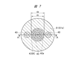
- FIG. 7 is a plan view showing the cathode in the second modification of the first embodiment
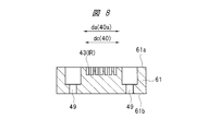
- FIG. 8 is a cross-sectional view showing the cathode in the second modification of the first embodiment.
- FIG. 8 is a sectional view taken along line AA in FIG.
- the cathode 61 has a front surface 61a and a back surface 61b, and is formed in a disc shape from pure iron as a conductive magnetic material.
- the cathode 61 is provided with a screw fixing hole 49 for fixing the cathode 61 to the base 17.
- the unevenness IR formed in the region 40 facing the inside of the ionization chamber IC in the surface 61a of the cathode 61 is in the region 40 facing the inside of the ionization chamber IC in the surface 61a of the cathode 61.
- It consists of the grooves 43 as a plurality of formed grooves.
- the plurality of grooves 43 are formed in a circular shape when viewed from the direction perpendicular to the surface 61a, that is, the Z-axis direction (see FIG. 2).
- the plurality of grooves 43 are formed concentrically when viewed from the Z-axis direction (see FIG. 2).
- the depth of the groove 43 is preferably 1 mm or more.
- the depth of the groove 43 is less than 1 mm, for example, when the cathode 61 is used for an accumulated time of about 1000 hours in normal operation, the surface 61a of the cathode 61 may be sputtered and scraped, and the groove 43 may disappear. There is. On the other hand, since the groove 43 does not have to penetrate the cathode 61, the depth of the groove 43 can be less than the thickness of the cathode 61.
- the unevenness IR is 0.4 mm.
- a circumferential groove 43 having a width and a depth of 1 mm can be formed.
- the region 40 is preferably surrounded by the inner peripheral surface of the cylindrical anode 13 when viewed from the Z-axis direction (see FIG. 2). This is a circular region included in the circular region 40a.
- the diameter da of the region 40a and the diameter dc of the region 40 satisfy the above formula (1).
- the diameter dc of the region 40 can be set to 70 mm or more and less than 100 mm.
- a circumferential groove 43 is formed, which is easier to manufacture than the case of forming a plurality of holes 41 (see FIGS. 3 and 4). Compared to 1, the manufacturing cost can be reduced.
- FIG. 9 is a cross-sectional view showing the configuration of the ion gun of Comparative Example 1.
- the ion gun IG 100 in the comparative example 1 also includes the gas supply mechanism 10, the cathode 111, the cathode 12, the anode 13, the permanent magnet 14, the acceleration electrode 15, and the insulator 16. , And base 17.
- the ion gun IG100 includes a discharge power supply 21 and an acceleration power supply 22.
- the gas supply mechanism 10, the cathode 111, the cathode 12, the anode 13, and the permanent magnet 14 constitute an ion generation part GP.
- the acceleration electrode 15 constitutes the ion ejection part IP.
- the cathode 111, the cathode 12, and the permanent magnet 14 define the ionization chamber IC.
- the ion gun IG100 of Comparative Example 1 is the same as the ion gun IG of Embodiment 1 except that the unevenness IR (see FIG. 2) is not formed on the surface of the cathode 111.
- the electrons emitted from the cathode 111 are rotated by the magnetic field generated by the permanent magnet 14, that is, swung to collide with the gas supplied by the gas supply mechanism 10.
- glow discharge is performed in the ionization chamber IC to generate argon ions as cations.
- a part of the argon ions generated in the ionization chamber IC passes through the ion beam passage hole 31 of the cathode 12, is accelerated by the acceleration electrode 15, and is emitted from the ion beam passage hole 33 as an ion beam IB (see FIG. 1). Is done.
- argon ions which are cations generated in the ionization chamber IC
- a part of the argon ions are accelerated toward the cathode 111 inside the ion gun IG100, and collide with a region facing the inside of the ionization chamber IC in the surface of the cathode 111.
- the surface of the cathode 111 is sputtered, and most of the sputtered particles emitted from the surface of the cathode 111 are deposited on the surface of the anode 13.
- the cathode 111 is made of a magnetic conductor such as pure iron, the sputtered particles are also made of a magnetic conductor. Therefore, the deposited film in which the sputtered particles are deposited on the surface of the anode 13 is the direction of the magnetic field generated by the permanent magnet 14. It grows in a needle shape along. A discharge voltage is applied between the cathode 111 and the anode 13 by the discharge power source 21. Therefore, abnormal discharge occurs between the cathode 111 and the anode 13 via a deposited film in which sputtered particles are deposited on the anode 13.
- a power supply circuit that applies a voltage between the cathode 111 and the anode 13 is short-circuited due to abnormal discharge, and a predetermined voltage is no longer applied between the cathode 111 and the anode 13.
- a predetermined voltage is no longer applied between the cathode 111 and the anode 13.
- FIG. 10 is a cross-sectional view showing the configuration of the ion gun of Comparative Example 2.
- the ion gun IG 200 in the comparative example 2 also includes the gas supply mechanism 10, the cathode 211, the cathode 12, the anode 13, the permanent magnet 14, the acceleration electrode 15, and the insulator 16. , And base 17.
- the ion gun IG 200 includes a discharge power source 21 and an acceleration power source 22.
- the gas supply mechanism 10, the cathode 211, the cathode 12, the anode 13, and the permanent magnet 14 constitute an ion generation part GP.
- the acceleration electrode 15 constitutes the ion ejection part IP.
- the cathode 211, the cathode 12, and the permanent magnet 14 define the ionization chamber IC.
- the cathode 211 is disposed on the surface of the main body 211a and the main body 211a in order to avoid the phenomenon that the ion beam is not emitted from the ion gun as the integration time of ion milling increases.
- a nonmagnetic material having conductivity that is, a nonmagnetic portion 211b made of a nonmagnetic conductor. Accordingly, the ion gun IG200 of Comparative Example 2 is the same as the ion gun IG100 of Comparative Example 1 except that the surface of the cathode 211 is made of a nonmagnetic conductor.
- the ion gun IG200 of Comparative Example 2 has the same structure as the ion gun described in Patent Document 2.
- sputtered particles emitted from the surface of the cathode 211 are deposited on the surface of the anode 13, but the sputtered particles are made of a nonmagnetic conductor. It is not laminated in the shape of a needle on the surface of 13.
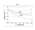
- FIG. 11 is a graph showing an example of the relationship between the milling integration time and the amount of change in the discharge current in the ion guns of Comparative Example 1 and Comparative Example 2.
- FIG. 12 is a graph showing an example of the relationship between the milling integration time and the amount of change in the ion beam current in the ion guns of Comparative Examples 1 and 2.
- the discharge current indicates the stability of the ion gun, and the ion beam current indicates the ion beam intensity, both of which are parameters that reflect the state of the ion gun.
- a measured value of the discharge current for example, a measured value obtained by measuring a current flowing between the discharge power source 21 and the anode 13 can be used.
- As a measured value of the ion beam current for example, when a shutter is disposed between the ion gun and the sample stage 8, a measured value of the current flowing through the shutter can be used.
- the cathode 111, the body 211a of the cathode 211, and the cathode 12 are made of pure iron as a magnetic conductor, and the anode 13 is made of aluminum as a nonmagnetic conductor. did.
- the insulator 16 is made of alumina as a nonmagnetic insulator, the acceleration electrode 15 is made of stainless steel as a nonmagnetic conductor, and the permanent magnet 14 is made of a neodymium magnet as a magnetic conductor. It was.
- the nonmagnetic portion 211b of the cathode 211 is made of titanium as a nonmagnetic conductor.
- Comparative Example 1 abnormal discharge tends to occur inside the ion gun as the milling integration time elapses, and the ion gun cannot be operated normally for a long time. Further, in Comparative Example 2, as the milling integration time elapses, the surface of the anode is covered with the insulating film, and the function as the anode electrode is lowered, so that the ion gun cannot be operated normally for a long time.
- FIG. 13 is a graph showing an example of the relationship between the milling integration time and the change amount of the discharge current in the ion guns of Example 1 and Comparative Example 1.
- FIG. 14 is a graph showing an example of the relationship between the milling integration time and the amount of change in the ion beam current in the ion guns of Example 1 and Comparative Example 1.
- Example 1 shown in FIGS. 13 and 14 is an example of the first embodiment (the same applies to FIG. 15 described later).
- the cathode 11 and the cathode 12 were made of pure iron as a magnetic conductor
- the anode 13 was made of aluminum as a nonmagnetic conductor.
- the insulator 16 is made of alumina as a nonmagnetic insulator
- the acceleration electrode 15 is made of stainless steel as a nonmagnetic conductor
- the permanent magnet 14 is made of a neodymium magnet as a magnetic conductor. It was.
- the amount of change that is, the amount of decrease since the start of milling of the discharge current and ion beam current in Example 1 is the discharge current in Comparative Example 1.
- the ion beam current is reduced to about 50% of the amount of decrease from the start of milling.
- the sputtering yield is reduced because the irradiation angle at which the cations are irradiated to the bottom of the unevenness IR is limited to a narrow range centering on the direction perpendicular to the surface 11a of the cathode 11, so that the sputtered particles are reduced. It is considered that the amount deposited on the inner peripheral surface of the anode 13 could be reduced. In addition, it is considered that the amount of sputtered particles deposited on the inner peripheral surface of the anode 13 could be reduced because the sputtered particles emitted from the bottom of the concave / convex IR reattached to the inside of the concave / convex IR.
- the ion gun can be operated normally for a long time without causing abnormal discharge inside the ion gun.
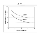
- FIG. 15 shows that the unevenness IR is formed in the region 40 facing the inside of the ionization chamber IC in the surface 11a of the cathode 11 to reduce the amount of sputtered particles deposited on the inner peripheral surface of the anode 13.
- FIG. 15 is a graph showing an example of the relationship between the distance from the end face in the ion gun of Example 1 and Comparative Example 1 and the growth rate of the deposited film.
- the distance from the end surface on the horizontal axis means the distance in the Z-axis direction (see FIG. 2) from the end surface on the cathode 11 side of the anode 13, and the growth rate of the deposited film on the vertical axis is the anode 13 means the growth rate of the deposited film deposited on the inner peripheral surface.
- the growth rate of the deposited film in Example 1 is about 80% of the growth rate of the deposited film in Comparative Example 1 at a position where the distance from the end face is about 1 mm, that is, the position on the cathode 11 side. Reduced. Further, the growth rate of the deposited film in Example 1 is reduced to about 50% of the growth rate of the deposited film in Comparative Example 1 at a position where the distance from the end face is about 6 mm, that is, the position on the cathode 12 side.
- the unevenness IR is formed in the region 40 facing the inside of the ionization chamber IC in the surface 11a of the cathode 11, the amount of sputtered particles emitted from the surface 11a of the cathode 11 can be reduced, and the sputtered particles It is considered that the amount deposited on the inner peripheral surface of the anode 13 could be reduced.
- the unevenness IR is formed in the region 40 facing the inside of the ionization chamber IC on the surface of the cathode 11.
- the irradiation angle at which the cations are irradiated on the bottom of the irregularities IR is limited to a narrow range centering on the direction perpendicular to the surface of the cathode 11, thereby reducing the sputtering yield.
- the sputtered particles emitted from the bottom of the unevenness IR are reattached inside the unevenness IR. Furthermore, the sputtered particles emitted from the unevenness IR are scattered.
- the amount of sputtered particles deposited on the inner peripheral surface of the anode 13 can be reduced. Therefore, in the ion gun and the ion milling apparatus, the ion gun can be operated normally for a long time without causing abnormal discharge inside the ion gun.
- the cathode 11 is integrally formed, and the unevenness IR is formed on the surface 11a of the integrally formed cathode 11 (see FIGS. 3 and 4).
- the attachment portion 71f is detachably attached to the main body portion 71c of the cathode 71, and the unevenness IR is formed on the surface 71d of the attachment portion 71f (FIGS. 16 to 18 described later). reference).
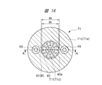
- FIG. 16 is a plan view showing the cathode according to the second embodiment
- FIG. 17 is a cross-sectional view showing the main body of the cathode according to the second embodiment
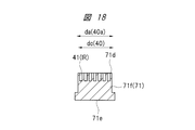
- FIG. 18 is a mounting portion of the cathode according to the second embodiment.
- FIG. 17 and 18 are cross-sectional views along the line AA in FIG.
- the cathode 71 includes a main body portion 71c having a front surface 71a and a back surface 71b, and a mounting portion 71f having a front surface 71d and a back surface 71e.
- the main body 71c is formed in a disk shape, and a screw fixing hole 49 for fixing the main body 71c to the base 17 with a screw is formed in the main body 71c.
- the main body 71c is made of a conductive magnetic material, that is, a magnetic conductor.
- a hole 75 as an opening is formed in the center of the main body 71c.
- the hole 75 has a step in the middle of the main body portion 71c in the thickness direction so that, for example, the opening area on the front surface 71a side of the main body portion 71c is smaller than the opening area on the back surface 71b side.
- the attachment portion 71f is detachably attached to the hole 75, and has a step in the thickness direction of the attachment portion 71f so that the area of the front surface 71d is smaller than the area of the back surface 71e. It has a shape corresponding to The attachment portion 71f is made of a conductive magnetic material, that is, a magnetic conductor.
- Such an attachment portion 71f is fitted into the hole 75 by being fitted into the hole 75 from the back surface 71b side of the main body portion 71c, and the main body portion 71c having the attachment portion 71f attached to the hole 75 is screwed to the base 17, for example, It is fixed by being stopped.
- the main body 71c faces the inside of the ionization chamber IC
- the hole 75 is formed in the region 40 facing the inside of the ionization chamber IC in the surface 71a of the main body 71c.
- the attachment portion 71f attached to 75 faces the inside of the ionization chamber IC.
- a plurality of holes 41 are formed on the surface 71d of the attachment portion 71f attached to the hole 75. That is, in the second embodiment, the unevenness IR formed on the surface 71d of the attachment portion 71f is composed of a plurality of holes 41.
- a hole 75 is formed in a region 40 having a diameter of 5.6 mm ⁇ at the center of the cathode 71, and the surface 71 d of the attachment portion 71 f attached to the hole 75 has an irregularity IR of 0.4 mm.
- Thirty-one holes 41 having a diameter of 1 mm and a depth of 1 mm can be formed.
- the cathode 71 can function as the cathode similar to the cathode 11 of the first embodiment.
- 16 to 18 show a case where the shape of the region 40 and the shape of the inner periphery on the surface 71a side of the hole 75 and the outer periphery of the surface 71d of the attachment portion 71f are the same. However, the shape of the region 40 and the shape of the inner periphery on the surface 71a side of the hole 75 and the outer periphery of the surface 71d of the attachment portion 71f may not coincide with each other.
- the unevenness IR is formed on the surface 71d of the attachment portion 71f that is detachably attached to the main body portion 71c.
- the surface 71d of the mounting portion 71f and the surface 42d of the mounting portion 71f are roughened (see FIG. 5 and FIG. 6) may be formed.
- a plurality of circumferential grooves 43 are formed on the surface 71d of the attachment portion 71f as the unevenness IR. May be formed.
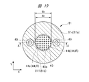
- FIG. 19 is a plan view showing the cathode in the first modification of the second embodiment
- FIG. 20 is a cross-sectional view showing the main body of the cathode in the first modification of the second embodiment
- FIG. 10 is a cross-sectional view showing a cathode mounting portion in a first modification of the second embodiment.
- 20 and 21 are sectional views taken along the line AA in FIG.
- the cathode 81 includes a main body portion 81c having a front surface 81a and a back surface 81b, and a mounting portion 81f having a front surface 81d and a back surface 81e.
- the main body portion 81c is formed in a disc shape, and a screw fixing hole 49 for fixing the main body portion 81c to the base 17 with a screw is formed in the main body portion 81c.
- the main body 81c is made of a conductive magnetic material, that is, a magnetic conductor.
- a hole 85 as an opening is formed at the center of the main body 81c.
- the hole 85 has a step in the middle of the body portion 81c in the thickness direction so that, for example, the opening area on the front surface 81a side of the body portion 81c is smaller than the opening area on the back surface 81b side.
- the attachment portion 81f is detachably attached to the hole 85, and has a step in the thickness direction of the attachment portion 81f so that the area of the front surface 81d is smaller than the area of the back surface 81e. It has a shape corresponding to The attachment portion 81f is made of a conductive magnetic material, that is, a magnetic conductor.
- Such a mounting portion 81f is fitted into the hole 85 by being fitted into the hole 85 from the back surface 81b side of the main body portion 81c. It is fixed by being stopped.
- the main body portion 81c faces the inside of the ionization chamber IC, and a hole 85 is formed in a region 40 facing the inside of the ionization chamber IC in the surface 81a of the main body portion 81c.
- the attachment part 81f attached to 85 faces the inside of the ionization chamber IC.
- grooves 44 as lattice-like grooves are formed on the surface 81d of the attachment portion 81f attached to the hole 85. That is, in the first modification, the unevenness IR formed on the surface 81d of the attachment portion 81f is composed of the lattice-shaped grooves 44.
- the cathode 81 can function as the cathode similar to the cathode 11 of the first embodiment, and the amount of sputtered particles emitted from the surface of the cathode 81 deposited on the inner peripheral surface of the anode 13 is reduced. Can do.
- the groove 44a and the groove 44b extending in two directions intersecting each other, for example, the Y-axis direction and the X-axis direction in FIG.
- the grooves 44 are formed in a lattice shape by being arranged in a direction intersecting with the extending direction.
- the groove 44 only the groove 44a extending in one direction, for example, the Y-axis direction in FIG. 19, intersects the extending direction in the surface 81d of the mounting portion 81f. You may form so that it may arrange in the direction to do.
- the unevenness IR is formed on the surface 81d of the attachment portion 81f that is detachably attached to the main body portion 81c.
- the groove 44 in the first modification example is provided on the surface 11a of the cathode 11 in the region 40 facing the inside of the ionization chamber IC, instead of the hole 41 (see FIGS. 3 and 4). It may be formed.
- the unevenness IR is formed in the region 40 facing the inside of the ionization chamber IC on the surface of the cathode 71.
- the irradiation angle at which the cations are irradiated to the bottom of the unevenness IR is limited to a narrow range centering on the direction perpendicular to the surface of the cathode 71, thereby reducing the sputtering yield.
- the sputtered particles emitted from the bottom of the unevenness IR are reattached inside the unevenness IR. Furthermore, the sputtered particles emitted from the unevenness IR are scattered.
- the second embodiment can also reduce the amount of sputtered particles deposited on the inner peripheral surface of the anode 13 as in the first embodiment. Therefore, in the ion gun and the ion milling apparatus, the ion gun can be operated normally for a long time without causing abnormal discharge inside the ion gun.
- the unevenness IR is formed on the surface of the attachment portion 71f that is detachably attached to the main body portion 71c.
- the cathode 11 is integrally formed, and the unevenness IR is formed on the surface 11a of the integrally formed cathode 11 (see FIGS. 3 and 4).
- a plate 91f as an attachment portion is detachably attached to the surface 91a of the main body portion 91c of the cathode 91, and unevenness IR is formed on the surface 91d of the plate 91f (described later). (See FIG. 22 and FIG. 23).
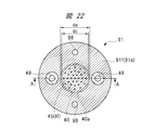
- FIG. 22 is a plan view showing the cathode in the third embodiment
- FIG. 23 is a cross-sectional view showing the cathode in the third embodiment.
- FIG. 23 is a cross-sectional view taken along line AA in FIG.
- the cathode 91 includes a main body portion 91c having a front surface 91a and a back surface 91b, and a plate 91f having a front surface 91d and a back surface 91e.
- the main body portion 91c is formed in a disc shape, and a screw fixing hole 49 for fixing the main body portion 91c to the base 17 with a screw is formed in the main body portion 91c.
- the main body 91c is made of a conductive magnetic material, that is, a magnetic conductor.
- the plate 91f is detachably attached to the surface 91a of the main body 91c.
- the plate 91f is made of a conductive magnetic material, that is, a magnetic conductor.
- the plate 91f is formed with a screw fixing hole 98 for fixing the plate 91f to the main body portion 91c with a screw.
- the plate 91f is attached to the front surface 91a of the main body 91c by, for example, screwing the main body 91c with the back surface 91e of the plate 91f facing the front surface 91a of the main body 91c. And the main-body part 91c by which the plate 91f was attached to the surface 91a is being fixed by screwing to the base 17, for example.
- the plate 91f attached to the surface 91a of the main body 91c faces the inside of the ionization chamber IC.
- a plurality of holes as through holes penetrating the plate 91f are formed in the region 40 facing the inside of the ionization chamber IC in the surface 91d of the plate 91f attached to the surface 91a of the main body 91c. 45 is formed. That is, in the third embodiment, the unevenness IR formed on the surface 91d of the plate 91f is composed of a plurality of holes 45.
- the cathode 91 can function as a cathode similar to the cathode 11 of the first embodiment.
- the hole 45 is formed in a truncated cone shape or a truncated pyramid shape, and the opening area of the hole 45 on the main body portion 91c side is larger than the opening area of the hole 45 on the opposite side to the main body portion 91c side. That is, preferably, the opening area of the hole 45 in the front surface 91d is smaller than the opening area of the hole 45 in the back surface 91e, and the hole 45 has an inversely tapered shape.
- the sputtered particles sputtered from the bottom of the hole 45 are more likely to be reattached to the inside of the hole 45, so that the sputtered particles are less than the case where the hole 45 as the unevenness IR does not have a reverse tapered shape.
- the amount deposited on the inner peripheral surface of the anode 13 can be further reduced. Therefore, in the ion gun and the ion milling apparatus, the ion gun can be operated normally for a longer time without causing abnormal discharge inside the ion gun.
- the surface 91d of the plate 91f is formed in the region 40 facing the inside of the ionization chamber IC in the surface 91d of the plate 91f as the unevenness IR.
- a rough surface 42 (see FIGS. 5 and 6) having a roughened surface may be formed.
- a plurality of circumferential shapes are formed in the region 40 facing the inside of the ionization chamber IC in the surface 91d of the plate 91f as the unevenness IR.
- the groove 43 (see FIGS. 7 and 8) may be formed.
- a lattice-like groove 44 is formed in the region 40 facing the inside of the ionization chamber IC on the surface 91d of the plate 91f as the unevenness IR. (See FIGS. 19 to 21) may be formed, and grooves extending only in one direction may be arranged in a direction intersecting with the extending direction.
- the unevenness IR is formed in the region 40 facing the inside of the ionization chamber IC on the surface of the cathode 91.
- the sputtering angle is reduced by limiting the irradiation angle at which the cations are irradiated to the bottom of the unevenness IR to a narrow range centering on the direction perpendicular to the surface of the cathode 91.
- the sputtered particles emitted from the bottom of the unevenness IR are reattached inside the unevenness IR. Furthermore, the sputtered particles emitted from the unevenness IR are scattered.
- the third embodiment can also reduce the amount of sputtered particles deposited on the inner peripheral surface of the anode 13 as in the first embodiment. Therefore, in the ion gun and the ion milling apparatus, the ion gun can be operated normally for a long time without causing abnormal discharge inside the ion gun.
- the unevenness IR is formed on the surface of the plate 91f detachably attached to the main body 91c.
- the cathode 91 when the cathode 91 is made of a member formed integrally, it is not easy to form the hole 45 having a reverse taper shape on the surface of the cathode 91, and the manufacturing cost of the cathode 91 may increase.
- the hole 91 having a tapered shape is easily formed from the back surface 91e of the plate 91f, and the plate 91f in which the hole 45 is formed is attached to the surface 91a of the main body 91c, whereby the cathode 91 A hole 45 having an inversely tapered shape on the surface can be easily formed. Therefore, the manufacturing cost of the cathode can be easily reduced.
- the present invention is effective when applied to an ion source and an ion milling apparatus.
- Sample stage 8 Sample stage 9
- Sample stage drive unit 10 Gas supply mechanism 11, 12, 51, 61, 71, 81, 91 Cathode 11a, 51a, 61a, 71a, 71d, 81a, 81d, 91a, 91d Surface 11b , 51b, 61b, 71b, 71e, 81b, 81e, 91b, 91e Back surface 13 Anode 13a, 15a Tubular portion 13b, 15b Bottom portion 14 Permanent magnet 15 Accelerating electrode 16 Insulator 17 Base 18, 19, 45, 75, 85 Hole 21 Discharge power source 22 Acceleration power source 31 to 33 Ion beam passage hole 40, 40a Region 41 Hole 42 Concavities and convexities 43, 44, 44a, 44b Groove 49, 98 Screw fixing holes 71c, 81c, 91c Body portion 71f, 81f Mounting portion 91f Plate da , Dc diameter GC ion gun controller GP ion generator IB Io Ion
Landscapes
- Chemical & Material Sciences (AREA)
- Analytical Chemistry (AREA)
- Engineering & Computer Science (AREA)
- Combustion & Propulsion (AREA)
- Electron Sources, Ion Sources (AREA)
Abstract
イオンガン(IG)は、イオン化室(IC)と、イオン化室(IC)でイオンを生成するイオン生成部(GP)とを有する。イオン生成部(GP)は、アノード(13)、カソード(11)、ガス供給機構(10)および永久磁石(14)を含む。イオン生成部(GP)は、カソード(11)により放出された電子を、永久磁石(14)が発生した磁場により旋回させて、ガス供給機構(10)により供給されたガスに衝突させることで、イオン化室(IC)でイオンを生成する。そして、カソード(11)の表面のうちイオン化室(IC)に面した領域(40)に、凹凸(IR)が形成されている。
Description
本発明はイオン源およびイオンミリング装置に関する。
イオンミリング法は、加速したイオンを試料に衝突させて、イオンが原子や分子をはじき飛ばすスパッタ現象を利用して、試料を削る加工法である。イオンミリング法では、試料の上面にイオンビームの遮蔽板となるマスクを載せた状態で、試料にイオンビームを照射し、試料のうちマスクの端部から突出した部分がイオンによりスパッタされることで、平滑な断面を加工することができる。この方法によれば、金属、ガラス、セラミックス、電子部品または複合材料などからなる試料を加工することができる。例えば電子部品からなる試料について、内部構造、断面形状もしくは膜厚の評価、または、結晶状態、故障または異物の断面の解析などを目的とし、走査型電子顕微鏡による形態像、試料組成像もしくはチャネリング像の取得、X線分析または結晶方位解析などを行うために、イオンミリング法が利用されている。
このようなイオンミリング法を行うためのイオンミリング装置においては、イオン源としてペニング型イオンガンが用いられている。ペニング型イオンガンは、ガス供給機構と、アノードと、カソードと、永久磁石とを備えている。このようなペニング型イオンガンにおいて、容易に放電を開始するため、および、放電を安定に維持するためには、カソードからの多くの電子放出が必要である。特開昭53-114661号公報(特許文献1)には、このようなペニング型イオンガンの構造が開示されている。
特開2006-351374号公報(特許文献2)には、イオンガンを構成するカソードの表面を、導電性を有する非磁性材料、すなわち非磁性体で形成するようにしたイオンガンの構造が記載されている。このようなイオンガンの構造において、イオンガンの内部で発生した陽イオンの衝突によりスパッタされた非磁性体の粒子は、アノードの内面上に堆積するが、従来のようにアノード上に針状に堆積されることはなく、異常放電を防止できることが開示されている。
特開2007-305485号公報(特許文献3)には、アーク放電装置において、チャンバーの内部に設けられたライナベースの表面に格子状の溝部を形成して不要な堆積物の大きさを規制することで、ライナベースと電極との絶縁不良を防止する方法が記載されている。
このようなペニング型イオンガンでは、カソードにより放出された電子を、永久磁石が発生した磁場により回転、すなわち旋回させて、ガス供給機構により供給されたガスに衝突させることで、イオン化室で陽イオンであるアルゴンイオンを生成する。また、イオン化室で生成されたアルゴンイオンの一部は、カソードのイオンビーム通過孔を通り、加速電極により加速されてイオンビーム通過孔からイオンビームとして射出される。
このとき、イオン化室で発生した陽イオンであるアルゴンイオンの一部は、イオンガンの内部のカソードに向けて加速され、カソードの表面のうちイオン化室の内部に面した領域に衝突する。このイオンの衝突により、カソードの表面はスパッタされ、カソードの表面がスパッタされて放出された粒子、すなわちスパッタ粒子のほとんどは、アノードの表面に堆積する。
このとき、カソードが純鉄などの磁性導電体からなる場合、スパッタ粒子も磁性導電体からなるので、アノードの表面にスパッタ粒子が堆積した堆積膜は、永久磁石により発生した磁場の方向に沿って針状に成長する。また、カソードとアノードとの間には、放電電源により放電電圧が印加されている。そのため、カソードと、アノードとの間に、アノード上にスパッタ粒子が堆積した堆積膜を介して、異常放電が発生する。さらには異常放電によりカソードとアノードとの間に電圧を印加している電源回路が短絡し、カソードとアノードとの間に、所定の電圧が印加されなくなる。
その結果、イオンミリングを行う時間を積算した積算時間の増加に伴って、カソードから電子が放出される放出量が減少するか、または、0になり、イオンガンからイオンビームが射出されなくなる現象が発生する。つまり、ミリング積算時間の増加に伴って、イオンガンの内部で異常放電が発生しやすくなり、イオンガンを長時間にわたって正常に動作させることができない。
一方、上記したような、ミリング積算時間の増加に伴って、イオンビームが射出されなくなるという現象を回避するために、カソードが、本体部と、本体部の表面に配置された導電性を有する非磁性材料、すなわち非磁性導電体からなる非磁性部とを含むものとすることがある。しかし、非磁性部を例えば非磁性導電体としてのチタンからなるものとした場合、イオン化室で発生した陽イオンの一部が衝突することにより非磁性部の表面がスパッタされて放出された粒子は、主成分としてTiOxを含む。TiOxは電気絶縁性を有する材料、すなわち絶縁体からなるため、TiOxが堆積して形成された絶縁膜によりアノードの表面が被覆されることで、アノードの電極としての機能が低下し、イオンガンを長時間にわたって正常に動作させることができない。
そこで、本発明は、イオン源としてのイオンガンの内部で異常放電が発生することなく、長時間にわたって正常に動作させることができるイオン源およびイオンミリング装置を提供する。
代表的な実施の形態によるイオン源は、第1室と、第1室でガスをイオン化してイオンを生成するイオン生成部とを有する。イオン生成部は、第1室に設けられたアノードと、第1室に面して設けられ、電子を放出する第1カソードと、第1室にガスを供給するガス供給部と、第1室に磁場を発生させる磁場発生部とを含む。イオン生成部は、第1カソードにより放出された電子を、磁場発生部が発生した磁場により旋回させて、ガス供給部により供給されたガスに衝突させることで、第1室でイオンを生成するものである。そして、第1カソードの表面のうち第1室に面した第1領域に、凹凸が形成されている。
また、代表的な実施の形態によるイオンミリング装置は、気密に設けられた第1室と、第1室を真空排気する真空排気部と、第1室で試料を保持する試料保持部と、試料保持部に保持された試料に向けてイオンを射出して試料を加工するイオン源とを有する。イオン源は、第2室と、第2室に形成された孔部と、第2室でガスをイオン化してイオンを生成するイオン生成部と、第2室で生成されたイオンを、孔部を通して第2室から射出するイオン射出部とを有し、第2室は、孔部を介して第1室と連通している。イオン生成部は、第2室に設けられたアノードと、第2室に面して設けられ、電子を放出する第1カソードと、第2室にガスを供給するガス供給部と、第2室に磁場を発生させる磁場発生部とを含む。イオン生成部は、第1カソードにより放出された電子を、磁場発生部が発生した磁場により旋回させて、ガス供給部により供給されたガスに衝突させることで、第2室でイオンを生成するものである。そして、第1カソードの表面のうち第2室に面した第1領域に、凹凸が形成されている。
代表的な実施の形態によれば、イオン源およびイオンミリング装置において、イオン源としてのイオンガンの内部で異常放電が発生することなく、長時間にわたって正常に動作させることができる。
以下の実施の形態においては便宜上その必要があるときは、複数のセクションまたは実施の形態に分割して説明するが、特に明示した場合を除き、それらはお互いに無関係なものではなく、一方は他方の一部または全部の変形例、詳細、補足説明等の関係にある。
また、以下の実施の形態において、要素の数等(個数、数値、量、範囲等を含む)に言及する場合、特に明示した場合および原理的に明らかに特定の数に限定される場合等を除き、その特定の数に限定されるものではなく、特定の数以上でも以下でもよい。
さらに、以下の実施の形態において、その構成要素(要素ステップ等も含む)は、特に明示した場合および原理的に明らかに必須であると考えられる場合等を除き、必ずしも必須のものではないことはいうまでもない。同様に、以下の実施の形態において、構成要素等の形状、位置関係等に言及するときは、特に明示した場合および原理的に明らかにそうでないと考えられる場合等を除き、実質的にその形状等に近似または類似するもの等を含むものとする。このことは、上記数値および範囲についても同様である。
以下、本発明の実施の形態を図面に基づいて詳細に説明する。なお、実施の形態を説明するための全図において、同一の機能を有する部材には同一の符号を付し、その繰り返しの説明は省略する。また、以下の実施の形態では、特に必要なとき以外は同一または同様な部分の説明を原則として繰り返さない。
さらに、実施の形態で用いる図面においては、断面図であっても図面を見やすくするためにハッチングを省略する場合もある。また、平面図であっても図面を見やすくするためにハッチングを付す場合もある。
また、以下の実施の形態において、A~Bとして範囲を示す場合には、特に明示した場合を除き、A以上B以下を示すものとする。
なお、以下に説明する各実施の形態では、イオン源を、イオンビーム加工装置としてのイオンミリング装置のイオン源に適用した場合を例に挙げて説明を行う。しかし、各実施の形態のイオン源は、イオンミリング装置のみならず、イオンビームを試料に照射し、二次的に発生した二次電子や反射電子を検出するSIM(Scanning Ion Microscope)またはイオンビームを使用したイオン顕微鏡など、他の各種のイオンビーム照射装置に適用可能である。また、以下に説明する各実施の形態は、本発明の要旨を逸脱しない範囲で適宜組み合わせることが可能である。
(実施の形態1)
<イオンミリング装置の構成>
図1は、実施の形態1のイオンミリング装置の全体構成図である。
<イオンミリング装置の構成>
図1は、実施の形態1のイオンミリング装置の全体構成図である。
図1に示すように、イオンミリング装置は、真空チャンバーVCと、真空排気系VPと、試料保持部SPと、イオンガンIGとを有する。
真空チャンバーVCは、気密に設けられており、内部で試料をミリング、すなわち加工する加工室である。真空排気系VPは、真空チャンバーVCの内部を真空排気する真空排気部である。真空チャンバーVCの内部の圧力は、真空排気系VPによって大気圧または真空に制御される。
試料保持部SPは、真空チャンバーVCの内部で試料6を保持する。試料保持部SPは、試料台7、試料ステージ8および試料ステージ駆動部9を含む。試料6は、試料台7の上に保持され、試料台7は、試料ステージ8に保持されている。試料ステージ8は、真空チャンバーVCが大気開放されたときに真空チャンバーVCの外へ引き出すことができるように構成されており、また試料6をイオンビームIBの光軸に対して任意の角度に傾斜させることができるように構成されている。試料ステージ駆動部9は、試料ステージ8を左右へスイングすることができ、その速度を制御することができる。
イオンガンIGは、イオンガンIGの内部でイオンを生成し、生成されたイオンを、試料保持部SPに保持された試料6に向けて射出し、射出されたイオンからなるイオンビームIBを試料6に照射し、試料6を加工するイオン源である。このイオンビームIBの照射とその電流密度は、イオンガン制御部GCによって制御される。
<イオンガンの構成>
図2は、実施の形態1のイオンガンの構成を示す断面図である。
図2は、実施の形態1のイオンガンの構成を示す断面図である。
図2に示すように、イオンガンIGは、イオン化室ICと、イオン生成部GPと、イオン射出部IPとを有する。イオン生成部GPは、イオン化室ICでガスをイオン化してイオンを生成する。イオン射出部IPは、イオン化室ICで生成されたイオンを、イオン化室ICに形成された孔部を通してイオン化室ICから射出する。
イオンガンIGは、ガス供給機構10と、カソード11と、カソード12と、アノード13と、永久磁石14と、加速電極15と、インシュレータ16と、ベース17とを含む。また、イオンガンIGは、放電電源21と、加速電源22とを含む。このうち、ガス供給機構10、カソード11、カソード12、アノード13および永久磁石14は、イオン生成部GPを構成する。一方、加速電極15は、イオン射出部IPを構成する。
ガス供給機構10は、イオン化室ICにガスを供給するガス供給部である。カソード11は、イオン化室ICの内部に面して設けられており、アノード13に対して負の電圧が印加され、電子を放出する。カソード12は、イオン化室ICの内部に面して設けられており、アノード13に対して負の電圧が印加され、電子を放出する。アノード13は、イオン化室ICの内部に設けられており、カソード11およびカソード12に対して正の電圧が印加される。永久磁石14は、イオン化室ICの内部に磁場を発生させる磁場発生部である。カソード11、カソード12、アノード13、永久磁石14、加速電極15およびインシュレータ16は、ベース17に固定されている。
カソード11は、例えば純鉄など導電性のある磁性材料からなり、かつ、円盤状に形成されている。すなわち、カソード11は、磁性導電体からなり、かつ、円板状に形成されている。カソード11は、ベース17に例えばネジ止めされることで、固定されている。カソード11には、カソード11を貫通する孔18が形成されている。孔18は、イオン化室ICに例えばアルゴンガスなどのガスを導入するためのものである。また、カソード11の形状は、円板状に限定されない。したがって、カソード11は、板状に形成されていてもよい。
本実施の形態1では、カソード11の表面のうちイオン化室ICの内部に面した領域40に凹凸IRが形成されている。なお、カソード11の具体的な構造については、後述する。
カソード12は、例えば純鉄など導電性のある磁性材料からなり、かつ、円盤状に形成されている。すなわち、カソード12は、磁性導電体からなり、かつ、円板状に形成されている。カソード12の中央部には、イオンビームを通過させるためのイオンビーム通過孔31が形成されている。また、カソード12の形状は、円板状に限定されない。したがって、カソード12は、板状に形成されていてもよい。
永久磁石14は、例えばネオジム磁石など、強磁性金属を含めた導電性を有する強磁性材料からなり、かつ、図2のZ軸方向に延びる円筒状に形成されている。カソード11は、永久磁石14のZ軸方向の一端、すなわち一方の端部に磁力により吸着されており、永久磁石14の一端は、カソード11に繋がっている。また、カソード12は、永久磁石14のZ軸方向の他端、すなわち他方の端部に磁力により吸着されており、カソード12は、永久磁石14の他端に繋がっている。そして、カソード11、カソード12および永久磁石14は、互いに電気的に接続されるので、カソード11、カソード12および永久磁石14は、互いに等電位に保たれる。
永久磁石14、カソード11およびカソード12により、イオン化室ICが区画されており、イオンビーム通過孔31は、イオン化室ICに形成された孔部である。このとき、永久磁石14は、イオン化室ICの内部に磁場を発生させる。また、カソード11およびカソード12は、磁路を形成しているので、カソード11およびカソード12により、イオン化室ICの内部に発生する磁場を強めることができる。
なお、永久磁石14に代え、電磁石などを用いることもできる。また、永久磁石14の形状は、円筒状に限定されない。したがって、永久磁石14は、筒状に形成されていてもよい。
インシュレータ16は、図2のZ軸方向に延びる円筒状に形成されている。インシュレータ16は、永久磁石14の内側に配置されており、インシュレータ16の外周面は、永久磁石14の内周面に接触している。インシュレータ16は、例えばセラミックスなどの電気絶縁性を有する非磁性材料で形成されている。
アノード13は、筒状部13aおよび底部13bを含み、例えばアルミニウムなど導電性を有する非磁性材料からなる。すなわち、アノード13は、非磁性導電体からなる。筒状部13aは、図2のZ軸方向に延びる円筒状に形成されており、インシュレータ16の内側に嵌め込まれている。筒状部13aの外周面は、インシュレータ16の内周面に接触しており、筒状部13aの内周面は、イオン化室ICの内部に面している。底部13bは、筒状部13aのベース17と反対側に形成されており、底部13bの中央部には、イオンビーム通過孔32が設けられている。アノード13は、インシュレータ16により、カソード11、カソード12および永久磁石14に対して電気的に絶縁されている。また、アノード13の形状は、円筒状に限定されない。したがって、アノード13は、筒状に形成されていてもよい。
加速電極15は、イオンビーム通過孔31を挟んでイオン化室ICの内部と反対側に設けられている。加速電極15は、筒状部15aおよび底部15bを含み、例えばステンレスなどの導電性を有する非磁性材料からなる。筒状部15aは、図2のZ軸方向に延び、イオン化室ICを囲む円筒状に形成されており、Z軸方向の一方の端部が、ベース17に固定されている。底部15bは、筒状部15aのベース17と反対側に形成されており、底部15bの中央部には、イオンビーム通過孔33が設けられている。加速電極15は、カソード11とカソード12と永久磁石14とを囲むように、ベース17の周辺部に固定されており、接地電位に保たれている。また、加速電極15の形状は、円筒状に限定されない。したがって、加速電極15は、筒状に形成されていてもよい。
なお、イオン化室ICは、カソード12に形成されたイオンビーム通過孔31、および、加速電極15に形成されたイオンビーム通過孔33を介して、加工室としての真空チャンバーVC(図1参照)と連通している。
ベース17には、当該ベース17を貫通し、カソード11を貫通する孔18と連通する孔19が形成されている。ガス供給機構10は、孔19および孔18を通してイオン化室ICにガスを導入できるように、ベース17に接続されている。ガス供給機構10は、イオン化室ICに供給するガスの流量を調整する。
放電電源21の一方の端子は、カソード11およびカソード12と電気的に接続されており、放電電源21の他方の端子は、アノード13と電気的に接続されており、カソード11およびカソード12と、アノード13との間には、放電電源21により放電電圧が印加される。加速電源22の一方の端子は、カソード11およびカソード12と電気的に接続されており、加速電源22の他方の端子は、加速電極15と電気的に接続されており、カソード11およびカソード12と、加速電極15との間には、加速電源22により加速電圧が印加される。また、放電電源21および加速電源22は、イオンガン制御部GCに接続されており、イオンガン制御部GCは、放電電源21の放電電圧、および、加速電源22の加速電圧を制御している。
次に、イオン生成部GPによりイオン化室ICの内部でガスをイオン化してイオンを生成する方法について説明する。なお、以下では、イオン化されるガスがアルゴンガスである場合について説明するが、本実施の形態1のイオン源によりイオン化されるガスはアルゴンガスに限定されない。
前述したように、ベース17およびカソード11には、孔19および孔18が形成されており、ガス供給機構10からのアルゴンガスは、孔19および孔18を通ってイオン化室ICに供給される。
イオン化室ICに供給されたアルゴンガスの分圧が適切な分圧を維持するように制御した状態で、アノード13に対してカソード11およびカソード12に負の電圧が印加されるように、カソード11およびカソード12と、アノード13との間に、放電電源21により0~4kV程度の放電電圧を印加する。また、前述したように、カソード11、カソード12および永久磁石14は、互いに電気的に接続されるので、カソード11、カソード12および永久磁石14は、互いに等電位に保たれる。これにより、カソード11により放出された電子を、ガス供給機構10により供給されたガスに衝突させることで、イオン化室ICでグロー放電させてアルゴンイオンを生成する。
本実施の形態1では、好適には、カソード11により放出された電子を、永久磁石14が発生した磁場により回転、すなわち旋回させて、ガス供給機構10により供給されたガスに衝突させることで、イオン化室ICでグロー放電させて陽イオンであるアルゴンイオンを生成する。このように、電子を磁場により回転させることで、電子が移動するパス、すなわち移動距離が長くなり、ガスに衝突しやすくなるので、放電効率を増加させることができる。
さらに、イオン化室ICに陽イオンであるアルゴンイオンが生成されている状態で、カソード11およびカソード12に対して加速電極15に負の電圧が印加されるように、カソード11およびカソード12と加速電極15との間に、加速電源22により0~10kV程度の加速電圧を印加する。これにより、イオン化室ICで生成されたアルゴンイオンの一部は、カソード12のイオンビーム通過孔31を通り、加速電極15により加速されてイオンビーム通過孔33からイオンビームIB(図1参照)として射出される。すなわち、イオン化室ICで生成された陽イオンであるアルゴンイオンを、イオン化室ICの内部からイオンビーム通過孔31を通してイオン化室ICの外部、つまり真空チャンバーVC(図1参照)の内部に射出する。これにより、図1に示すように、陽イオンからなるイオンビームIBが試料6に照射され、試料6が加工される。
一方、イオン化室ICで発生した陽イオンであるアルゴンイオンの一部は、イオン化室ICの内部に面したカソード11に向けて加速され、カソード11の表面のうちイオン化室ICの内部に面した領域に衝突する。このイオンの衝突により、カソード11の表面はスパッタされ、カソード11の表面から放出されたスパッタ粒子のほとんどは、アノード13の表面に堆積する。
本実施の形態1では、カソード11の表面のうちイオン化室ICの内部に面した領域40に、凹凸IRが形成されている。これにより、凹凸IRの底部に陽イオンが照射される照射角度が、カソード11の表面に対して垂直な方向を中心とする狭い範囲に制限されることでスパッタ収率が低減する。また、凹凸IRの底部から放出されたスパッタ粒子が凹凸IRの内部に再付着する。さらに、凹凸IRから放出されたスパッタ粒子が散乱される。これらの理由により、本実施の形態1では、スパッタ粒子がアノード13の内周面へ堆積する量を低減することができる。したがって、イオンガンおよびイオンミリング装置において、イオンガンで異常放電が発生することなく、長時間にわたって正常に動作させることができる。
<カソードの構成>
次に、カソードの具体的な構成について説明する。図3は、実施の形態1におけるカソードを示す平面図であり、図4は、実施の形態1におけるカソードを示す断面図である。図4は、図3のA-A線に沿った断面図である。
次に、カソードの具体的な構成について説明する。図3は、実施の形態1におけるカソードを示す平面図であり、図4は、実施の形態1におけるカソードを示す断面図である。図4は、図3のA-A線に沿った断面図である。
図3および図4に示すように、カソード11は、表面11aおよび裏面11bを有し、円盤状に形成されている。また、カソード11には、カソード11をベース17にネジで固定するためのネジ固定用孔49が形成されている。カソード11は、導電性のある磁性材料、すなわち磁性導電体からなる。
なお、表面11aおよび裏面11bについては、カソード11がイオン化室ICに面する側を表面11aとし、表面11aと反対側を裏面11bとする。
本実施の形態1では、カソード11の表面11aのうちイオン化室ICの内部に面した領域40に形成された凹凸IRは、カソード11の表面11aのうちイオン化室ICの内部に面した領域40に形成された複数の穴部としての穴41からなる。複数の穴41の各々の深さとして、好適には、1mm以上とすることができる。穴41の深さが1mm未満の場合、例えばカソード11を通常の運用において1000時間程度の積算時間の間使用したときに、カソード11の表面11aがスパッタされて削られて穴41が消失するおそれがある。一方、穴41がカソード11を貫通しなければよいので、穴41の深さとしては、カソード11の厚さ未満とすることができる。
具体的には、カソード11の表面11aのうちイオン化室ICの内部に面した領域40として、例えばカソード11の中心部における5.6mmφの直径を有する領域40に、凹凸IRとして、0.4mmの直径および1mmの深さを有する穴41を、31個形成することができる。領域40の面積に対して穴41が占める面積の比率は、約20%である。
本実施の形態1では、穴41として、平面視において、円形状の穴を形成しているが、穴41としては、カソード11の表面11aに凹凸を形成するものであれば円形状の穴に限定されるものではなく、平面視において、多角形状の穴を形成してもよい。ただし、容易に製造することができるという観点から、穴41として、図3に示すように、平面視において、円形状の穴を形成することが好ましい。
なお、平面視においてとは、穴41が形成されているカソード11の表面11aに垂直な方向から穴41を視た場合を意味し、カソード11の表面11aに平行な方向を図2におけるX軸方向とするとき、カソード11の表面11aに垂直な方向とは、図2におけるZ軸方向を意味する。
好適には、領域40は、Z軸方向(図2参照)から視たときに、円筒状のアノード13の内周面に囲まれた円状の領域40aに内包された円状の領域である。円筒状のアノード13の直上の領域である領域40aにおいてカソード11の表面11aにアルゴンイオンが衝突する量は、領域40a以外の領域においてカソード11の表面11aにアルゴンイオンが衝突する量に比べ、多い。したがって、円筒状のアノード13の内周面に囲まれた領域40aに内包された領域40において、カソード11の表面11aに、穴41からなる凹凸IRを形成することにより、スパッタ粒子がアノード13の内周面へ堆積する量を低減する効果をより大きくすることができる。
なお、アノード13が筒状ではあるが円筒状ではなく、筒状のアノード13が延びる方向がカソード11の表面に垂直でない場合には、領域40は、好適には、筒状のアノード13が延びる方向から視たときに、筒状のアノード13の内周面に囲まれた領域40aに内包されている。
さらに好適には、円状の領域40が、円状の領域40aの中心の位置と同一の位置を中心とする領域である場合には、アノード13の内径、すなわち円状の領域40aの直径を直径daとし、円状の領域40の直径を直径dcとしたとき、直径daおよび直径dcは、下記式(1)
dc≧0.7da 式(1)
の条件を満たしている。具体的には、例えば領域40aの直径daが100mmである場合、領域40の直径dcを70mm以上100mm未満とすることができる。
dc≧0.7da 式(1)
の条件を満たしている。具体的には、例えば領域40aの直径daが100mmである場合、領域40の直径dcを70mm以上100mm未満とすることができる。
Z軸方向(図2参照)から視たときに、式(1)の条件を満たす円状の領域40は、円状の領域40aの中心部である。円状の領域40aの中心部である円状の領域40においてカソード11の表面11aにアルゴンイオンが衝突する量は、領域40a以外の領域においてカソード11の表面11aにアルゴンイオンが衝突する量に比べ、極めて多い。したがって、円筒状のアノード13の内周面に囲まれた領域40aに内包された領域40において、カソード11の表面11aに、穴41からなる凹凸IRを形成することにより、スパッタ粒子がアノード13の内周面へ堆積する量を低減する効果をさらに大きくすることができる。
式(1)の条件を満たさない場合、すなわち直径dcが直径daの0.7倍未満の場合、領域40aの内部であって領域40の外部の領域においてカソード11の表面にアルゴンイオンが衝突する量が多くなる。したがって、スパッタ収率が低減する効果、スパッタ粒子が凹凸IRの内部に再付着する効果、および、スパッタ粒子が散乱される効果が小さくなるおそれがある。一方、式(1)の条件を満たす場合、スパッタ収率が低減する効果、スパッタ粒子が凹凸IRの内部に再付着する効果、または、スパッタ粒子が散乱される効果が大きくなるので、スパッタ粒子がアノード13の内周面へ堆積する量を低減することができる。
なお、円状の領域40が、円状の領域40aの中心と同一の位置を中心とする領域でなくても、円状の領域40aの中心付近の位置を中心とする領域である場合には、式(1)を満たすことにより、同様の効果を得ることができる。
<カソードの第1変形例>
図5は、実施の形態1の第1変形例におけるカソードを示す平面図であり、図6は、実施の形態1の第1変形例におけるカソードを示す断面図である。図6は、図5のA-A線に沿った断面図である。
図5は、実施の形態1の第1変形例におけるカソードを示す平面図であり、図6は、実施の形態1の第1変形例におけるカソードを示す断面図である。図6は、図5のA-A線に沿った断面図である。
図5および図6に示すように、カソード51は、表面51aおよび裏面51bを有し、導電性のある磁性材料として純鉄により円盤状に形成されている。また、カソード51には、カソード51をベース17に固定するためのネジ固定用孔49が設けられている。
本第1変形例では、凹凸IRとして、カソード51の表面51aのうちイオン化室ICの内部に面した領域40に、カソード51の表面51aが粗面化された凹凸42が形成されている。カソード51の表面51aが粗面化された凹凸42の平均粗さは、50μm以上である。ここで、平均粗さは、算術平均粗さRaを意味する。凹凸42の平均粗さが50μm未満の場合、凹凸42の粗さが小さくなりすぎて、スパッタ収率が低減する効果、スパッタ粒子が凹凸IRの内部に再付着する効果、および、スパッタ粒子が散乱される効果が小さくなるおそれがある。したがって、凹凸42の平均粗さを50μm以上とすることで、スパッタ収率が低減する効果、スパッタ粒子が凹凸IRの内部に再付着する効果、または、スパッタ粒子が散乱される効果が大きくなるので、スパッタ粒子がアノード13の内周面へ堆積する量を低減することができる。
本第1変形例でも、実施の形態1と同様に、好適には、領域40は、Z軸方向(図2参照)から視たときに、円筒状のアノード13の内周面に囲まれた円状の領域40aに内包された円状の領域である。これにより、実施の形態1と同様に、スパッタ粒子がアノード13の内周面へ堆積する量を低減する効果をより大きくすることができる。
また、本第1変形例でも、実施の形態1と同様に、さらに好適には、領域40aの直径daと、領域40の直径dcとが上記式(1)を満たしている。具体的には、例えば領域40aの直径daが100mmである場合、領域40の直径dcを70mm以上100mm未満とすることができる。これにより、実施の形態1と同様に、スパッタ粒子がアノード13の内周面へ堆積する量を低減する効果をさらに大きくすることができる。
一方、本第1変形例では、カソード51の表面51aを粗面化するものであり、複数の穴41(図3および図4参照)を形成する場合よりも製造が容易であるため、実施の形態1に比べ、製造コストを低減することができる。なお、カソード51の表面51aの全面が粗面化されていてもよい。
<カソードの第2変形例>
図7は、実施の形態1の第2変形例におけるカソードを示す平面図であり、図8は、実施の形態1の第2変形例におけるカソードを示す断面図である。図8は、図7のA-A線に沿った断面図である。
図7は、実施の形態1の第2変形例におけるカソードを示す平面図であり、図8は、実施の形態1の第2変形例におけるカソードを示す断面図である。図8は、図7のA-A線に沿った断面図である。
図7および図8に示すように、カソード61は、表面61aおよび裏面61bを有し、導電性のある磁性材料として純鉄により円盤状に形成されている。また、カソード61には、カソード61をベース17に固定するためのネジ固定用孔49が設けられている。
本第2変形例では、カソード61の表面61aのうちイオン化室ICの内部に面した領域40に形成された凹凸IRは、カソード61の表面61aのうちイオン化室ICの内部に面した領域40に形成された複数の溝部としての溝43からなる。複数の溝43は、表面61aに垂直な方向、すなわちZ軸方向(図2参照)から視たときに、円周状に形成されている。また、好適には、複数の溝43は、Z軸方向(図2参照)から視たときに、同心円状に形成されている。溝43の深さとして、好適には、1mm以上とすることができる。溝43の深さが1mm未満の場合、例えばカソード61を通常の運用において1000時間程度の積算時間の間使用したときに、カソード61の表面61aがスパッタされて削られて溝43が消失するおそれがある。一方、溝43がカソード61を貫通しなければよいので、溝43の深さとしては、カソード61の厚さ未満とすることができる。
具体的には、カソード61の表面61aのうちイオン化室ICの内部に面した領域40として、例えばカソード61の中心部における5.6mmφの直径を有する領域40に、凹凸IRとして、0.4mmの幅および1mmの深さを有する円周状の溝43を、形成することができる。
本第2変形例でも、実施の形態1と同様に、好適には、領域40は、Z軸方向(図2参照)から視たときに、円筒状のアノード13の内周面に囲まれた円状の領域40aに内包された円状の領域である。これにより、実施の形態1と同様に、スパッタ粒子がアノード13の内周面へ堆積する量を低減する効果をより大きくすることができる。
また、本第2変形例でも、実施の形態1と同様に、さらに好適には、領域40aの直径daと、領域40の直径dcとが上記式(1)を満たしている。具体的には、例えば領域40aの直径daが100mmである場合、領域40の直径dcを70mm以上100mm未満とすることができる。これにより、実施の形態1と同様に、スパッタ粒子がアノード13の内周面へ堆積する量を低減する効果をさらに大きくすることができる。
一方、本第2変形例では、円周状の溝43を形成するものであり、複数の穴41(図3および図4参照)を形成する場合よりも製造が容易であるため、実施の形態1に比べ、製造コストを低減することができる。
<放電電流およびイオンビーム電極の経時変化について>
図9は、比較例1のイオンガンの構成を示す断面図である。比較例1におけるイオンガンIG100も、実施の形態1におけるイオンガンIGと同様に、ガス供給機構10と、カソード111と、カソード12と、アノード13と、永久磁石14と、加速電極15と、インシュレータ16と、ベース17とを含む。また、イオンガンIG100は、放電電源21と、加速電源22とを含む。このうち、ガス供給機構10、カソード111、カソード12、アノード13および永久磁石14は、イオン生成部GPを構成する。一方、加速電極15は、イオン射出部IPを構成する。また、カソード111、カソード12および永久磁石14は、イオン化室ICを区画する。
図9は、比較例1のイオンガンの構成を示す断面図である。比較例1におけるイオンガンIG100も、実施の形態1におけるイオンガンIGと同様に、ガス供給機構10と、カソード111と、カソード12と、アノード13と、永久磁石14と、加速電極15と、インシュレータ16と、ベース17とを含む。また、イオンガンIG100は、放電電源21と、加速電源22とを含む。このうち、ガス供給機構10、カソード111、カソード12、アノード13および永久磁石14は、イオン生成部GPを構成する。一方、加速電極15は、イオン射出部IPを構成する。また、カソード111、カソード12および永久磁石14は、イオン化室ICを区画する。
比較例1のイオンガンIG100は、カソード111の表面に凹凸IR(図2参照)が形成されていない点を除き、実施の形態1のイオンガンIGと同様である。
比較例1では、実施の形態1と同様に、カソード111により放出された電子を、永久磁石14が発生した磁場により回転、すなわち旋回させて、ガス供給機構10により供給されたガスに衝突させることで、イオン化室ICでグロー放電させて陽イオンであるアルゴンイオンを生成する。また、イオン化室ICで生成されたアルゴンイオンの一部は、カソード12のイオンビーム通過孔31を通り、加速電極15により加速されてイオンビーム通過孔33からイオンビームIB(図1参照)として射出される。
このとき、イオン化室ICで発生した陽イオンであるアルゴンイオンの一部は、イオンガンIG100の内部のカソード111に向けて加速され、カソード111の表面のうちイオン化室ICの内部に面した領域に衝突する。このイオンの衝突により、カソード111の表面はスパッタされ、カソード111の表面から放出されたスパッタ粒子のほとんどは、アノード13の表面に堆積する。
このとき、カソード111が純鉄などの磁性導電体からなる場合、スパッタ粒子も磁性導電体からなるので、アノード13の表面にスパッタ粒子が堆積した堆積膜は、永久磁石14により発生した磁場の方向に沿って針状に成長する。また、カソード111とアノード13との間には、放電電源21により放電電圧が印加されている。そのため、カソード111と、アノード13との間に、アノード13上にスパッタ粒子が堆積した堆積膜を介して、異常放電が発生する。さらには異常放電によりカソード111とアノード13との間に電圧を印加している電源回路が短絡し、カソード111とアノード13との間に、所定の電圧が印加されなくなる。その結果、イオンミリングを行う時間を積算した積算時間の増加に伴って、カソード111から電子が放出される放出量が減少するか、または、0になり、イオンガンIG100からイオンビームが射出されなくなる現象が発生する。
図10は、比較例2のイオンガンの構成を示す断面図である。比較例2におけるイオンガンIG200も、実施の形態1におけるイオンガンIGと同様に、ガス供給機構10と、カソード211と、カソード12と、アノード13と、永久磁石14と、加速電極15と、インシュレータ16と、ベース17とを含む。また、イオンガンIG200は、放電電源21と、加速電源22とを含む。このうち、ガス供給機構10、カソード211、カソード12、アノード13および永久磁石14は、イオン生成部GPを構成する。一方、加速電極15は、イオン射出部IPを構成する。また、カソード211、カソード12および永久磁石14は、イオン化室ICを区画する。
比較例2のイオンガンIG200では、イオンミリングの積算時間の増加に伴って、イオンガンからイオンビームが射出されなくなる現象を回避するために、カソード211が、本体部211aと、本体部211aの表面に配置された導電性を有する非磁性材料、すなわち非磁性導電体からなる非磁性部211bとを含む。したがって、比較例2のイオンガンIG200は、カソード211の表面が非磁性導電体からなる点を除き、比較例1のイオンガンIG100と同様である。
比較例2のイオンガンIG200は、上記特許文献2に記載されたイオンガンとも同様の構造を有する。そして、このようなイオンガンの構造において、カソード211の表面から放出されたスパッタ粒子は、アノード13の表面に堆積はするものの、スパッタ粒子が非磁性導電体からなるため、磁場の方向に沿ってアノード13の表面に針状に積層されることはない。
図11は、比較例1および比較例2のイオンガンにおけるミリング積算時間と放電電流の変化量との関係の一例を示すグラフである。また、図12は、比較例1および比較例2のイオンガンにおけるミリング積算時間とイオンビーム電流の変化量との関係の一例を示すグラフである。放電電流は、イオンガンの安定度を示し、イオンビーム電流は、イオンビーム強度を示し、ともにイオンガンの状態を反映するパラメータである。放電電流の測定値として、例えば放電電源21とアノード13との間を流れる電流を測定した測定値とすることができる。イオンビーム電流の測定値として、例えばイオンガンと試料ステージ8との間にシャッタを配置したとき、シャッタに流れる電流を測定した測定値とすることができる。
比較例1および比較例2では、カソード111、カソード211の本体部211aおよびカソード12を、磁性導電体としての純鉄からなるものとし、アノード13を、非磁性導電体としてのアルミニウムからなるものとした。また、インシュレータ16を、非磁性絶縁体としてのアルミナからなるものとし、加速電極15を、非磁性導電体としてのステンレスからなるものとし、永久磁石14を、磁性導電体としてのネオジム磁石からなるものとした。また比較例2では、カソード211の非磁性部211bとして、非磁性導電体としてのチタンからなるものとした。
図11および図12に示すように、比較例1および比較例2では、イオン化室ICで発生した陽イオンの一部が衝突してカソード111および非磁性部211bの表面がスパッタされて放出された粒子がアノード13の表面に堆積することにより、放電電流値およびイオンビーム電流値はミリング積算時間の経過に伴って低下する。また、ミリング積算時間が等しい場合、比較例2における放電電流およびイオンビーム電流のミリング開始時からの変化量、すなわち低下量は、それぞれ比較例1における放電電流およびイオンビーム電流の低下量よりも大きい。
これは、比較例2では、イオン化室ICで発生した陽イオンの一部がカソード211の本体部211aの表面に配置された非磁性部211bに衝突し、このイオンの衝突により非磁性部211bの表面がスパッタされて放出された粒子が、主成分としてTiOxを含むことが影響している。TiOxは電気絶縁性を有する材料、すなわち絶縁体からなるため、TiOxが堆積して形成された絶縁膜によりアノード13の表面が被覆されることとなり、アノード13の電極としての機能が低下する。
したがって、比較例1では、ミリング積算時間の経過に伴って、イオンガンの内部で異常放電が発生しやすくなり、イオンガンを長時間にわたって正常に動作させることができない。また、比較例2では、ミリング積算時間の経過に伴って、アノードの表面が絶縁膜に被覆され、アノードの電極としての機能が低下するので、イオンガンを長時間にわたって正常に動作させることができない。
<本実施の形態の主要な特徴と効果>
図13は、実施例1および比較例1のイオンガンにおけるミリング積算時間と放電電流の変化量との関係の一例を示すグラフである。図14は、実施例1および比較例1のイオンガンにおけるミリング積算時間とイオンビーム電流の変化量との関係の一例を示すグラフである。
図13は、実施例1および比較例1のイオンガンにおけるミリング積算時間と放電電流の変化量との関係の一例を示すグラフである。図14は、実施例1および比較例1のイオンガンにおけるミリング積算時間とイオンビーム電流の変化量との関係の一例を示すグラフである。
図13および図14に示す実施例1は、本実施の形態1の実施例である(後述する図15においても同様)。実施例1では、カソード11およびカソード12を、磁性導電体としての純鉄からなるものとし、アノード13を、非磁性導電体としてのアルミニウムからなるものとした。また、インシュレータ16を、非磁性絶縁体としてのアルミナからなるものとし、加速電極15を、非磁性導電体としてのステンレスからなるものとし、永久磁石14を、磁性導電体としてのネオジム磁石からなるものとした。
図13および図14に示すように、ミリング積算時間が300時間である場合、実施例1における放電電流およびイオンビーム電流のミリング開始時からの変化量、すなわち低下量は、比較例1における放電電流およびイオンビーム電流のミリング開始時からの低下量に対し、50%程度に低減される。
これは、凹凸IRの底部に陽イオンが照射される照射角度が、カソード11の表面11aに対して垂直な方向を中心とする狭い範囲に制限されることでスパッタ収率が低減したため、スパッタ粒子がアノード13の内周面へ堆積する量を低減できたものと考えられる。また、凹凸IRの底部から放出されたスパッタ粒子が凹凸IRの内部に再付着したため、スパッタ粒子がアノード13の内周面へ堆積する量を低減できたものと考えられる。さらに、凹凸IRから放出されたスパッタ粒子が散乱されたため、スパッタ粒子がアノード13の内周面へ堆積する量を低減することができたものと考えられる。したがって、本実施の形態1では、イオンガンの内部で異常放電が発生することなく、イオンガンを長時間にわたって正常に動作させることができる。
カソード11の表面11aのうちイオン化室ICの内部に面した領域40に、凹凸IRが形成されたことで、スパッタ粒子のアノード13の内周面へ堆積する量を低減できることについては、図15を用いて説明することができる。図15は、実施例1および比較例1のイオンガンにおける端面からの距離と、堆積膜の成長速度との関係の一例を示すグラフである。図15において、横軸の端面からの距離とは、アノード13のカソード11側の端面からのZ軸方向(図2参照)の距離を意味し、縦軸の堆積膜の成長速度とは、アノード13の内周面に堆積される堆積膜の成長速度を意味する。
図15に示すように、実施例1における堆積膜の成長速度は、端面からの距離が1mm程度の位置、すなわちカソード11側の位置で、比較例1における堆積膜の成長速度の80%程度に低減される。また、実施例1における堆積膜の成長速度は、端面からの距離が6mm程度の位置、すなわちカソード12側の位置で、比較例1における堆積膜の成長速度の50%程度に低減される。すなわち、カソード11の表面11aのうちイオン化室ICの内部に面した領域40に、凹凸IRが形成されたことで、カソード11の表面11aから放出されるスパッタ粒子の放出量が低減でき、スパッタ粒子がアノード13の内周面へ堆積する量を低減することができたものと考えられる。
以上述べたように、本実施の形態1では、カソード11の表面のうちイオン化室ICの内部に面した領域40に、凹凸IRが形成されている。これにより、凹凸IRの底部に陽イオンが照射される照射角度が、カソード11の表面に対して垂直な方向を中心とする狭い範囲に制限されることでスパッタ収率が低減する。また、凹凸IRの底部から放出されたスパッタ粒子が凹凸IRの内部に再付着する。さらに、凹凸IRから放出されたスパッタ粒子が散乱される。これらの理由により、本実施の形態1では、スパッタ粒子がアノード13の内周面へ堆積する量を低減することができる。したがって、イオンガンおよびイオンミリング装置において、イオンガンの内部で異常放電が発生することなく、イオンガンを長時間にわたって正常に動作させることができる。
(実施の形態2)
実施の形態1では、カソード11は、一体に形成されており、一体に形成されたカソード11の表面11aに凹凸IRが形成されていた(図3および図4参照)。一方、実施の形態2では、カソード71の本体部71cに、取付部71fが着脱可能に取り付けられており、取付部71fの表面71dに凹凸IRが形成されている(後述する図16~図18参照)。
実施の形態1では、カソード11は、一体に形成されており、一体に形成されたカソード11の表面11aに凹凸IRが形成されていた(図3および図4参照)。一方、実施の形態2では、カソード71の本体部71cに、取付部71fが着脱可能に取り付けられており、取付部71fの表面71dに凹凸IRが形成されている(後述する図16~図18参照)。
実施の形態2のイオンミリング装置およびイオンガンのうちカソード71以外の部分については、実施の形態1と同様にすることができるため、その説明を省略する。
<カソードの構成>
図16は、実施の形態2におけるカソードを示す平面図であり、図17は、実施の形態2におけるカソードの本体部を示す断面図であり、図18は、実施の形態2におけるカソードの取付部を示す断面図である。図17および図18は、図16のA-A線に沿った断面図である。
図16は、実施の形態2におけるカソードを示す平面図であり、図17は、実施の形態2におけるカソードの本体部を示す断面図であり、図18は、実施の形態2におけるカソードの取付部を示す断面図である。図17および図18は、図16のA-A線に沿った断面図である。
図16~図18に示すように、カソード71は、表面71aおよび裏面71bを有する本体部71cと、表面71dおよび裏面71eを有する取付部71fとを含む。本体部71cは、円盤状に形成されており、本体部71cには、本体部71cをベース17にネジで固定するためのネジ固定用孔49が形成されている。本体部71cは、導電性のある磁性材料、すなわち磁性導電体からなる。
本体部71cの中央部には、開口部としての孔75が形成されている。孔75は、例えば本体部71cの表面71a側の開口面積が、裏面71b側の開口面積よりも小さくなるように、本体部71cの厚さ方向の途中に段差を有する。
取付部71fは、孔75に着脱可能に取り付けられており、表面71dの面積が、裏面71eの面積よりも小さくなるように、取付部71fの厚さ方向の途中に段差を有し、孔75に対応した形状を有する。取付部71fは、導電性のある磁性材料、すなわち磁性導電体からなる。
このような取付部71fは、本体部71cの裏面71b側から孔75に嵌め込まれることで、孔75に取り付けられ、孔75に取付部71fが取り付けられた本体部71cが、ベース17に例えばネジ止めされることで、固定されている。
本実施の形態2では、本体部71cはイオン化室ICの内部に面しており、本体部71cの表面71aのうちイオン化室ICの内部に面した領域40に孔75が形成されており、孔75に取り付けられた取付部71fは、イオン化室ICの内部に面している。また、本実施の形態2では、孔75に取り付けられた取付部71fの表面71dに、複数の穴41が形成されている。すなわち、本実施の形態2では、取付部71fの表面71dに形成される凹凸IRは、複数の穴41からなる。具体的には、例えばカソード71の中心部における5.6mmφの直径を有する領域40に、孔75を形成し、孔75に取り付けられた取付部71fの表面71dに、凹凸IRとして、0.4mmの直径および1mmの深さを有する穴41を、31個形成することができる。これにより、カソード71を、実施の形態1のカソード11と同様のカソードとして機能させることができる。
なお、図16~図18では、領域40の形状と、孔75の表面71a側の内周および取付部71fの表面71dの外周の形状とが、一致している場合を示す。しかし、領域40の形状と、孔75の表面71a側の内周および取付部71fの表面71dの外周の形状とは、一致していなくてもよい。
さらに、本実施の形態2では、本体部71cに着脱可能に取り付けられた取付部71fの表面71dに凹凸IRが形成されている。これにより、イオンガンで発生した陽イオンの一部がカソード71に衝突してカソード71の表面が削られることでイオンガンの性能が劣化した場合において、表面71dに凹凸IRが形成された取付部71fを着脱交換することで、容易に性能を復帰させることができる。そのため、メンテナンス性に優れたカソードを実現することができ、交換部品のコストを低減することができる。
なお、本実施の形態2でも、実施の形態1の第1変形例と同様に、凹凸IRとして、取付部71fの表面71dに、取付部71fの表面71dが粗面化された凹凸42(図5および図6参照)が形成されていてもよい。また、本実施の形態2でも、実施の形態1の第2変形例と同様に、凹凸IRとして、取付部71fの表面71dに、複数の円周状の溝43(図7および図8参照)が形成されていてもよい。
<カソードの第1変形例>
図19は、実施の形態2の第1変形例におけるカソードを示す平面図であり、図20は、実施の形態2の第1変形例におけるカソードの本体部を示す断面図であり、図21は、実施の形態2の第1変形例におけるカソードの取付部を示す断面図である。図20および図21は、図19のA-A線に沿った断面図である。
図19は、実施の形態2の第1変形例におけるカソードを示す平面図であり、図20は、実施の形態2の第1変形例におけるカソードの本体部を示す断面図であり、図21は、実施の形態2の第1変形例におけるカソードの取付部を示す断面図である。図20および図21は、図19のA-A線に沿った断面図である。
図19~図21に示すように、カソード81は、表面81aおよび裏面81bを有する本体部81cと、表面81dおよび裏面81eを有する取付部81fとを含む。本体部81cは、円盤状に形成されており、本体部81cには、本体部81cをベース17にネジで固定するためのネジ固定用孔49が形成されている。本体部81cは、導電性のある磁性材料、すなわち磁性導電体からなる。
本体部81cの中央部には、開口部としての孔85が形成されている。孔85は、例えば本体部81cの表面81a側の開口面積が、裏面81b側の開口面積よりも小さくなるように、本体部81cの厚さ方向の途中に段差を有する。
取付部81fは、孔85に着脱可能に取り付けられており、表面81dの面積が、裏面81eの面積よりも小さくなるように、取付部81fの厚さ方向の途中に段差を有し、孔85に対応した形状を有する。取付部81fは、導電性のある磁性材料、すなわち磁性導電体からなる。
このような取付部81fは、本体部81cの裏面81b側から孔85に嵌め込まれることで、孔85に取り付けられ、孔85に取付部81fが取り付けられた本体部81cが、ベース17に例えばネジ止めされることで、固定されている。
本第1変形例では、本体部81cはイオン化室ICの内部に面しており、本体部81cの表面81aのうちイオン化室ICの内部に面した領域40に孔85が形成されており、孔85に取り付けられた取付部81fは、イオン化室ICの内部に面している。また、本第1変形例では、孔85に取り付けられた取付部81fの表面81dに、格子状の溝部としての溝44が形成されている。すなわち、本第1変形例では、取付部81fの表面81dに形成される凹凸IRは、格子状の溝44からなる。これにより、カソード81を、実施の形態1のカソード11と同様のカソードとして機能させることができ、カソード81の表面から放出されたスパッタ粒子がアノード13の内周面へ堆積する量を低減することができる。
なお、図19に示す例では、取付部81fの表面81d内で、互いに交差する2つの方向、例えば図19のY軸方向およびX軸方向にそれぞれ延在する溝44aおよび溝44bが、それぞれの延在する方向と交差する方向に配列することで、溝44が格子状に形成されている。しかし、溝44として、取付部81fの表面81d内で、互いに交差する2つの方向のうち一方の方向、例えば図19のY軸方向に延在する溝44aのみが、その延在する方向と交差する方向に配列するように形成してもよい。
本第1変形例でも、実施の形態2と同様に、本体部81cに着脱可能に取り付けられた取付部81fの表面81dに凹凸IRが形成されている。これにより、イオンガンで発生した陽イオンの一部がカソード81に衝突してカソード81の表面が削られることでイオンガンの性能が劣化した場合において、表面81dに凹凸IRが形成された取付部81fを着脱交換することで、容易に性能を復帰させることができる。そのため、メンテナンス性に優れたカソードを実現することができ、交換部品のコストを低減することができる。
なお、前述した実施の形態1において、イオン化室ICの内部に面した領域40におけるカソード11の表面11aに、穴41(図3および図4参照)に代え、本第1変形例における溝44が形成されていてもよい。
<本実施の形態の主要な特徴と効果>
本実施の形態2でも、実施の形態1と同様に、カソード71の表面のうちイオン化室ICの内部に面した領域40に、凹凸IRが形成されている。これにより、凹凸IRの底部に陽イオンが照射される照射角度が、カソード71の表面に対して垂直な方向を中心とする狭い範囲に制限されることでスパッタ収率が低減する。また、凹凸IRの底部から放出されたスパッタ粒子が凹凸IRの内部に再付着する。さらに、凹凸IRから放出されたスパッタ粒子が散乱される。これらの理由により、本実施の形態2でも、実施の形態1と同様に、スパッタ粒子がアノード13の内周面へ堆積する量を低減することができる。したがって、イオンガンおよびイオンミリング装置において、イオンガンの内部で異常放電が発生することなく、イオンガンを長時間にわたって正常に動作させることができる。
本実施の形態2でも、実施の形態1と同様に、カソード71の表面のうちイオン化室ICの内部に面した領域40に、凹凸IRが形成されている。これにより、凹凸IRの底部に陽イオンが照射される照射角度が、カソード71の表面に対して垂直な方向を中心とする狭い範囲に制限されることでスパッタ収率が低減する。また、凹凸IRの底部から放出されたスパッタ粒子が凹凸IRの内部に再付着する。さらに、凹凸IRから放出されたスパッタ粒子が散乱される。これらの理由により、本実施の形態2でも、実施の形態1と同様に、スパッタ粒子がアノード13の内周面へ堆積する量を低減することができる。したがって、イオンガンおよびイオンミリング装置において、イオンガンの内部で異常放電が発生することなく、イオンガンを長時間にわたって正常に動作させることができる。
また、本実施の形態2では、本体部71cに着脱可能に取り付けられた取付部71fの表面に凹凸IRが形成されている。これにより、前述したように、メンテナンス性に優れたカソードを実現することができ、交換部品のコストを低減することができる。
(実施の形態3)
実施の形態1では、カソード11は、一体に形成されており、一体に形成されたカソード11の表面11aに凹凸IRが形成されていた(図3および図4参照)。一方、実施の形態3では、カソード91の本体部91cの表面91aに、取付部としてのプレート91fが着脱可能に取り付けられており、プレート91fの表面91dに凹凸IRが形成されている(後述する図22および図23参照)。
実施の形態1では、カソード11は、一体に形成されており、一体に形成されたカソード11の表面11aに凹凸IRが形成されていた(図3および図4参照)。一方、実施の形態3では、カソード91の本体部91cの表面91aに、取付部としてのプレート91fが着脱可能に取り付けられており、プレート91fの表面91dに凹凸IRが形成されている(後述する図22および図23参照)。
実施の形態3のイオンミリング装置およびイオンガンのうちカソード91以外の部分については、実施の形態1と同様にすることができるため、その説明を省略する。
<カソードの構成>
図22は、実施の形態3におけるカソードを示す平面図であり、図23は、実施の形態3におけるカソードを示す断面図である。図23は、図22のA-A線に沿った断面図である。
図22は、実施の形態3におけるカソードを示す平面図であり、図23は、実施の形態3におけるカソードを示す断面図である。図23は、図22のA-A線に沿った断面図である。
図22および図23に示すように、カソード91は、表面91aおよび裏面91bを有する本体部91cと、表面91dおよび裏面91eを有するプレート91fとを含む。本体部91cは、円盤状に形成されており、本体部91cには、本体部91cをベース17にネジで固定するためのネジ固定用孔49が形成されている。本体部91cは、導電性のある磁性材料、すなわち磁性導電体からなる。
プレート91fは、本体部91cの表面91aに着脱可能に取り付けられている。プレート91fは、導電性のある磁性材料、すなわち磁性導電体からなる。プレート91fには、プレート91fを本体部91cにネジで固定するためのネジ固定用孔98が形成されている。
このようなプレート91fは、プレート91fの裏面91eが本体部91cの表面91aと対向した状態で、本体部91cに例えばネジ止めされることで、本体部91cの表面91aに取り付けられている。そして、表面91aにプレート91fが取り付けられた本体部91cが、ベース17に例えばネジ止めされることで、固定されている。
本実施の形態3では、本体部91cの表面91aに取り付けられたプレート91fは、イオン化室ICの内部に面している。また、本実施の形態3では、本体部91cの表面91aに取り付けられたプレート91fの表面91dのうちイオン化室ICの内部に面した領域40に、プレート91fを貫通する貫通孔としての複数の孔45が形成されている。すなわち、本実施の形態3では、プレート91fの表面91dに形成される凹凸IRは、複数の孔45からなる。具体的には、カソード91のイオン化室ICの内部に面した領域40として、例えばプレート91fの中心部における5.6mmφの直径を有する領域40に、凹凸IRとして、孔45を31個形成することができる。これにより、カソード91を、実施の形態1のカソード11と同様のカソードとして機能させることができる。
好適には、孔45は、円錐台状または角錐台状に形成されており、孔45の本体部91c側の開口面積が、孔45の本体部91c側と反対側の開口面積よりも大きい。すなわち、好適には、表面91dにおける孔45の開口面積が、裏面91eにおける孔45の開口面積よりも小さく、孔45は、逆テーパ形状を有している。これにより、孔45の底部がスパッタされて放出されたスパッタ粒子が孔45の内部にさらに再付着しやすくなるため、凹凸IRとしての孔45が逆テーパ形状を有しない場合に比べ、スパッタ粒子がアノード13の内周面へ堆積する量をさらに低減することができる。したがって、イオンガンおよびイオンミリング装置において、イオンガンの内部で異常放電が発生することなく、イオンガンをさらに長時間にわたって正常に動作させることができる。
なお、本実施の形態3でも、実施の形態1の第1変形例と同様に、凹凸IRとして、プレート91fの表面91dのうちイオン化室ICの内部に面した領域40に、プレート91fの表面91dが粗面化された凹凸42(図5および図6参照)が形成されていてもよい。また、本実施の形態3でも、実施の形態1の第2変形例と同様に、凹凸IRとして、プレート91fの表面91dのうちイオン化室ICの内部に面した領域40に、複数の円周状の溝43(図7および図8参照)が形成されていてもよい。さらに、本実施の形態3でも、実施の形態2の第1変形例と同様に、凹凸IRとして、プレート91fの表面91dのうちイオン化室ICの内部に面した領域40に、格子状の溝44(図19~図21参照)が形成されていてもよく、また、一方向のみに延在する溝が、その延在する方向と交差する方向に配列されていてもよい。
<本実施の形態の主要な特徴と効果>
本実施の形態3でも、実施の形態1と同様に、カソード91の表面のうちイオン化室ICの内部に面した領域40に、凹凸IRが形成されている。これにより、凹凸IRの底部に陽イオンが照射される照射角度が、カソード91の表面に対して垂直な方向を中心とする狭い範囲に制限されることでスパッタ収率が低減する。また、凹凸IRの底部から放出されたスパッタ粒子が凹凸IRの内部に再付着する。さらに、凹凸IRから放出されたスパッタ粒子が散乱される。これらの理由により、本実施の形態3でも、実施の形態1と同様に、スパッタ粒子がアノード13の内周面へ堆積する量を低減することができる。したがって、イオンガンおよびイオンミリング装置において、イオンガンの内部で異常放電が発生することなく、イオンガンを長時間にわたって正常に動作させることができる。
本実施の形態3でも、実施の形態1と同様に、カソード91の表面のうちイオン化室ICの内部に面した領域40に、凹凸IRが形成されている。これにより、凹凸IRの底部に陽イオンが照射される照射角度が、カソード91の表面に対して垂直な方向を中心とする狭い範囲に制限されることでスパッタ収率が低減する。また、凹凸IRの底部から放出されたスパッタ粒子が凹凸IRの内部に再付着する。さらに、凹凸IRから放出されたスパッタ粒子が散乱される。これらの理由により、本実施の形態3でも、実施の形態1と同様に、スパッタ粒子がアノード13の内周面へ堆積する量を低減することができる。したがって、イオンガンおよびイオンミリング装置において、イオンガンの内部で異常放電が発生することなく、イオンガンを長時間にわたって正常に動作させることができる。
また、本実施の形態3では、本体部91cに着脱可能に取り付けられたプレート91fの表面に凹凸IRが形成されている。これにより、実施の形態2と同様に、メンテナンス性に優れたカソードを実現することができ、交換部品のコストを低減することができる。
さらに、カソード91が一体として形成された部材からなるときは、カソード91の表面に逆テーパ形状を有する孔45を形成することは容易ではなく、カソード91の製造コストが増加するおそれがある。しかし、本実施の形態3では、プレート91fの裏面91eからテーパ形状を有する孔45を容易に形成し、孔45が形成されたプレート91fを本体部91cの表面91aに取り付けることで、カソード91の表面に逆テーパ形状を有する孔45を容易に形成することができる。そのため、カソードの製造コストを容易に低減することができる。
以上、本発明者によってなされた発明をその実施の形態に基づき具体的に説明したが、本発明は前記実施の形態に限定されるものではなく、その要旨を逸脱しない範囲で種々変更可能であることはいうまでもない。
本発明は、イオン源およびイオンミリング装置に適用して有効である。
6 試料
7 試料台
8 試料ステージ
9 試料ステージ駆動部
10 ガス供給機構
11、12、51、61、71、81、91 カソード
11a、51a、61a、71a、71d、81a、81d、91a、91d 表面
11b、51b、61b、71b、71e、81b、81e、91b、91e 裏面
13 アノード
13a、15a 筒状部
13b、15b 底部
14 永久磁石
15 加速電極
16 インシュレータ
17 ベース
18、19、45、75、85 孔
21 放電電源
22 加速電源
31~33 イオンビーム通過孔
40、40a 領域
41 穴
42 凹凸
43、44、44a、44b 溝
49、98 ネジ固定用孔
71c、81c、91c 本体部
71f、81f 取付部
91f プレート
da、dc 直径
GC イオンガン制御部
GP イオン生成部
IB イオンビーム
IC イオン化室
IG イオンガン
IP イオン射出部
IR 凹凸
SP 試料保持部
VC 真空チャンバー
VP 真空排気系
7 試料台
8 試料ステージ
9 試料ステージ駆動部
10 ガス供給機構
11、12、51、61、71、81、91 カソード
11a、51a、61a、71a、71d、81a、81d、91a、91d 表面
11b、51b、61b、71b、71e、81b、81e、91b、91e 裏面
13 アノード
13a、15a 筒状部
13b、15b 底部
14 永久磁石
15 加速電極
16 インシュレータ
17 ベース
18、19、45、75、85 孔
21 放電電源
22 加速電源
31~33 イオンビーム通過孔
40、40a 領域
41 穴
42 凹凸
43、44、44a、44b 溝
49、98 ネジ固定用孔
71c、81c、91c 本体部
71f、81f 取付部
91f プレート
da、dc 直径
GC イオンガン制御部
GP イオン生成部
IB イオンビーム
IC イオン化室
IG イオンガン
IP イオン射出部
IR 凹凸
SP 試料保持部
VC 真空チャンバー
VP 真空排気系
Claims (15)
- 第1室と、
前記第1室でガスをイオン化してイオンを生成するイオン生成部と、
を有し、
前記イオン生成部は、
前記第1室に設けられたアノードと、
前記第1室に面して設けられ、電子を放出する第1カソードと、
前記第1室にガスを供給するガス供給部と、
前記第1室に磁場を発生させる磁場発生部と、
を含み、
前記第1カソードにより放出された電子を、前記磁場発生部が発生した磁場により旋回させて、前記ガス供給部により供給されたガスに衝突させることで、前記第1室でイオンを生成するものであり、
前記第1カソードの表面のうち前記第1室に面した第1領域に、凹凸が形成されている、イオン源。 - 請求項1記載のイオン源において、
前記アノードは、前記第1領域における前記第1カソードの表面に交差する第1方向に延びる筒状に形成されており、
前記第1カソードの表面のうち前記第1領域は、前記第1方向から視たときに、筒状の前記アノードの内周面に囲まれた第2領域に内包されている、イオン源。 - 請求項2記載のイオン源において、
前記アノードは、前記第1領域における前記第1カソードの表面に垂直な前記第1方向に延びる円筒状に形成されており、
前記第1カソードの表面のうち前記第1領域は、前記第1方向から視たときに、円筒状の前記アノードの内周面に囲まれた円状の前記第2領域に内包された円状の領域であり、
前記アノードの内径をdaとし、前記円状の前記第1領域の直径をdcとしたとき、dc≧0.7daの条件を満たしている、イオン源。 - 請求項1記載のイオン源において、
前記凹凸は、前記第1領域における前記第1カソードの表面が粗面化されたものであり、
粗面化された前記凹凸の平均粗さは、50μm以上である、イオン源。 - 請求項1記載のイオン源において、
前記凹凸は、前記第1領域における前記第1カソードの表面に形成された複数の穴部からなる、イオン源。 - 請求項5記載のイオン源において、
前記複数の穴部の各々の深さが1mm以上である、イオン源。 - 請求項1記載のイオン源において、
前記凹凸は、前記第1領域における前記第1カソードの表面に形成された複数の溝部からなる、イオン源。 - 請求項7記載のイオン源において、
前記複数の溝部の各々は、前記第1領域における前記第1カソードの表面に垂直な第2方向から視たときに、円周状である、イオン源。 - 請求項1記載のイオン源において、
前記凹凸は、前記第1領域における前記第1カソードの表面に形成された格子状の溝部からなる、イオン源。 - 請求項1記載のイオン源において、
前記第1カソードは、
第1本体部と、
前記第1本体部に形成された開口部と、
前記開口部に着脱可能に取り付けられた第1取付部と、
を含み、
前記第1本体部は、前記第1室に面しており、
前記開口部は、前記第1本体部の表面のうち前記第1室に面した前記第1領域に形成されており、
前記凹凸は、前記開口部に取り付けられた前記第1取付部の表面に形成されている、イオン源。 - 請求項1記載のイオン源において、
前記第1カソードは、
第2本体部と、
前記第2本体部の表面に着脱可能に取り付けられた第2取付部と、
を含み、
前記第2本体部の表面に取り付けられた前記第2取付部は、前記第1室に面しており、
前記凹凸は、前記第2本体部の表面に取り付けられた前記第2取付部の表面のうち前記第1室に面した前記第1領域に形成されている、イオン源。 - 請求項11記載のイオン源において、
前記凹凸は、前記第2取付部を貫通する複数の貫通孔からなり、
前記複数の貫通孔の各々は、円錐台状または角錐台状に形成されており、
前記貫通孔の前記第2本体部側の開口面積が、前記貫通孔の前記第2本体部側と反対側の開口面積よりも大きい、イオン源。 - 請求項1記載のイオン源において、
前記第1室に形成された孔部と、
前記第1室で生成されたイオンを、前記孔部を通して前記第1室から射出するイオン射出部と、
を有する、イオン源。 - 請求項2記載のイオン源において、
前記イオン生成部は、前記第1室に面して設けられた第2カソードを含み、
前記磁場発生部は、前記第1方向に延びる筒状の永久磁石であり、
前記第1カソードは、磁性導電体からなり、かつ、板状に形成されており、
前記第2カソードは、磁性導電体からなり、かつ、板状に形成されており、
前記第1カソードは、筒状の前記永久磁石の前記第1方向の一方の端部に吸着されており、
前記第2カソードは、筒状の前記永久磁石の前記第1方向の他方の端部に吸着されており、
前記第1室は、前記永久磁石、前記第1カソードおよび前記第2カソードにより区画されている、イオン源。 - 気密に設けられた第1室と、
前記第1室を真空排気する真空排気部と、
前記第1室で試料を保持する試料保持部と、
前記試料保持部に保持された試料に向けてイオンを射出して前記試料を加工するイオン源と、
を有し、
前記イオン源は、
第2室と、
前記第2室に形成された孔部と、
前記第2室でガスをイオン化してイオンを生成するイオン生成部と、
前記第2室で生成されたイオンを、前記孔部を通して前記第2室から射出するイオン射出部と、
を有し、
前記第2室は、前記孔部を介して前記第1室と連通しており、
前記イオン生成部は、
前記第2室に設けられたアノードと、
前記第2室に面して設けられ、電子を放出する第1カソードと、
前記第2室にガスを供給するガス供給部と、
前記第2室に磁場を発生させる磁場発生部と、
を含み、
前記第1カソードにより放出された電子を、前記磁場発生部が発生した磁場により旋回させて、前記ガス供給部により供給されたガスに衝突させることで、前記第2室でイオンを生成するものであり、
前記第1カソードの表面のうち前記第2室に面した第1領域に、凹凸が形成されている、イオンミリング装置。
Applications Claiming Priority (2)
| Application Number | Priority Date | Filing Date | Title |
|---|---|---|---|
| JP2013118326A JP6100619B2 (ja) | 2013-06-04 | 2013-06-04 | イオン源およびイオンミリング装置 |
| JP2013-118326 | 2013-06-04 |
Publications (1)
| Publication Number | Publication Date |
|---|---|
| WO2014196262A1 true WO2014196262A1 (ja) | 2014-12-11 |
Family
ID=52007916
Family Applications (1)
| Application Number | Title | Priority Date | Filing Date |
|---|---|---|---|
| PCT/JP2014/060102 Ceased WO2014196262A1 (ja) | 2013-06-04 | 2014-04-07 | イオン源およびイオンミリング装置 |
Country Status (3)
| Country | Link |
|---|---|
| JP (1) | JP6100619B2 (ja) |
| TW (1) | TW201511062A (ja) |
| WO (1) | WO2014196262A1 (ja) |
Cited By (2)
| Publication number | Priority date | Publication date | Assignee | Title |
|---|---|---|---|---|
| DE112015006787B4 (de) | 2015-09-25 | 2021-11-25 | Hitachi High-Tech Corporation | Ionenätzsystem |
| US20220285123A1 (en) * | 2019-08-28 | 2022-09-08 | Hitachi High-Tech Corporation | Ion gun and ion milling machine |
Families Citing this family (7)
| Publication number | Priority date | Publication date | Assignee | Title |
|---|---|---|---|---|
| WO2016189614A1 (ja) * | 2015-05-25 | 2016-12-01 | 株式会社日立ハイテクノロジーズ | イオンミリング装置、及びイオンミリング方法 |
| JP6741858B2 (ja) * | 2017-03-24 | 2020-08-19 | 株式会社日立ハイテク | 荷電粒子線装置 |
| US11508552B2 (en) * | 2018-08-31 | 2022-11-22 | Hitachi High-Tech Corporation | Ion milling device |
| JP7366152B2 (ja) * | 2019-12-24 | 2023-10-20 | 株式会社日立ハイテク | イオンミリング装置 |
| US11244800B2 (en) * | 2020-06-18 | 2022-02-08 | Axcelis Technologies, Inc. | Stepped indirectly heated cathode with improved shielding |
| KR102820384B1 (ko) | 2021-05-27 | 2025-06-16 | 주식회사 히타치하이테크 | 이온 밀링 장치 |
| KR20250032358A (ko) * | 2023-08-31 | 2025-03-07 | 삼성전자주식회사 | 라이너 구조물 및 이를 포함하는 기판 처리 장치 |
Citations (6)
| Publication number | Priority date | Publication date | Assignee | Title |
|---|---|---|---|---|
| US20020117637A1 (en) * | 2001-02-28 | 2002-08-29 | International Business Machines Corporation | Ion generation chamber |
| JP2004362937A (ja) * | 2003-06-04 | 2004-12-24 | Kobe Steel Ltd | イオン源 |
| JP2006351374A (ja) * | 2005-06-16 | 2006-12-28 | Jeol Ltd | イオン源 |
| JP2007305485A (ja) * | 2006-05-12 | 2007-11-22 | Matsushita Electric Ind Co Ltd | アーク放電装置及びそれを用いたイオン注入装置 |
| JP2010532082A (ja) * | 2007-06-26 | 2010-09-30 | ヴァリアン セミコンダクター イクイップメント アソシエイツ インコーポレイテッド | 電子生成及び集束用溝を有する陰極、イオン源及び関連方法 |
| WO2011127394A1 (en) * | 2010-04-09 | 2011-10-13 | E.A. Fischione Instruments, Inc. | Improved ion source |
-
2013
- 2013-06-04 JP JP2013118326A patent/JP6100619B2/ja active Active
-
2014
- 2014-04-07 WO PCT/JP2014/060102 patent/WO2014196262A1/ja not_active Ceased
- 2014-04-16 TW TW103113851A patent/TW201511062A/zh unknown
Patent Citations (6)
| Publication number | Priority date | Publication date | Assignee | Title |
|---|---|---|---|---|
| US20020117637A1 (en) * | 2001-02-28 | 2002-08-29 | International Business Machines Corporation | Ion generation chamber |
| JP2004362937A (ja) * | 2003-06-04 | 2004-12-24 | Kobe Steel Ltd | イオン源 |
| JP2006351374A (ja) * | 2005-06-16 | 2006-12-28 | Jeol Ltd | イオン源 |
| JP2007305485A (ja) * | 2006-05-12 | 2007-11-22 | Matsushita Electric Ind Co Ltd | アーク放電装置及びそれを用いたイオン注入装置 |
| JP2010532082A (ja) * | 2007-06-26 | 2010-09-30 | ヴァリアン セミコンダクター イクイップメント アソシエイツ インコーポレイテッド | 電子生成及び集束用溝を有する陰極、イオン源及び関連方法 |
| WO2011127394A1 (en) * | 2010-04-09 | 2011-10-13 | E.A. Fischione Instruments, Inc. | Improved ion source |
Cited By (3)
| Publication number | Priority date | Publication date | Assignee | Title |
|---|---|---|---|---|
| DE112015006787B4 (de) | 2015-09-25 | 2021-11-25 | Hitachi High-Tech Corporation | Ionenätzsystem |
| US20220285123A1 (en) * | 2019-08-28 | 2022-09-08 | Hitachi High-Tech Corporation | Ion gun and ion milling machine |
| US12051560B2 (en) * | 2019-08-28 | 2024-07-30 | Hitachi High-Tech Corporation | Ion gun and ion milling machine |
Also Published As
| Publication number | Publication date |
|---|---|
| TW201511062A (zh) | 2015-03-16 |
| JP6100619B2 (ja) | 2017-03-22 |
| JP2014235948A (ja) | 2014-12-15 |
Similar Documents
| Publication | Publication Date | Title |
|---|---|---|
| JP6100619B2 (ja) | イオン源およびイオンミリング装置 | |
| US11158481B2 (en) | Ion milling device, ion source, and ion milling method | |
| KR20080067966A (ko) | 박막 형성 장치 | |
| JP5903864B2 (ja) | イオンミリング装置 | |
| JP6637055B2 (ja) | イオンミリング装置 | |
| KR102520928B1 (ko) | 플라즈마 이온원 및 하전 입자 빔 장치 | |
| TWI743879B (zh) | 離子槍及離子銑削裝置 | |
| JP2006351374A (ja) | イオン源 | |
| JP2017174730A (ja) | 荷電粒子ビーム装置及びプラズマ点火方法 | |
| US20070256927A1 (en) | Coating Apparatus for the Coating of a Substrate and also Method for Coating | |
| WO2013099044A1 (ja) | イオンビーム処理装置および中和器 | |
| JP5325623B2 (ja) | 電子源 | |
| JP4810497B2 (ja) | 原子線源および表面改質装置 | |
| KR102417574B1 (ko) | 전리 진공계 및 카트리지 | |
| JP2018022701A (ja) | イオンガン及びイオンミリング装置、イオンミリング方法 | |
| JP5350911B2 (ja) | プラズマ発生装置及び成膜装置並びに成膜方法及び表示素子の製造方法 | |
| RU2504860C2 (ru) | Способ производства заготовок с травленной ионами поверхностью | |
| JP2013008471A (ja) | ガスイオン源 | |
| JP2008077857A (ja) | イオン銃、イオン銃を備える真空加工装置を利用する方法 | |
| JP2005290442A (ja) | Ecrスパッタリング装置 | |
| JP4647476B2 (ja) | 成膜装置 | |
| JP2018170295A (ja) | イオンガン及びイオンミリング装置、イオンミリング方法 |
Legal Events
| Date | Code | Title | Description |
|---|---|---|---|
| 121 | Ep: the epo has been informed by wipo that ep was designated in this application |
Ref document number: 14806958 Country of ref document: EP Kind code of ref document: A1 |
|
| NENP | Non-entry into the national phase |
Ref country code: DE |
|
| 122 | Ep: pct application non-entry in european phase |
Ref document number: 14806958 Country of ref document: EP Kind code of ref document: A1 |