WO2014196185A1 - マイクロチップおよびマイクロチップにおける金属薄膜の成膜方法 - Google Patents
マイクロチップおよびマイクロチップにおける金属薄膜の成膜方法 Download PDFInfo
- Publication number
- WO2014196185A1 WO2014196185A1 PCT/JP2014/002911 JP2014002911W WO2014196185A1 WO 2014196185 A1 WO2014196185 A1 WO 2014196185A1 JP 2014002911 W JP2014002911 W JP 2014002911W WO 2014196185 A1 WO2014196185 A1 WO 2014196185A1
- Authority
- WO
- WIPO (PCT)
- Prior art keywords
- substrate
- metal thin
- thin film
- microchip
- titanium oxide
- Prior art date
- Legal status (The legal status is an assumption and is not a legal conclusion. Google has not performed a legal analysis and makes no representation as to the accuracy of the status listed.)
- Ceased
Links
Images







Classifications
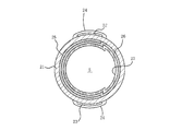
-
- G—PHYSICS
- G01—MEASURING; TESTING
- G01N—INVESTIGATING OR ANALYSING MATERIALS BY DETERMINING THEIR CHEMICAL OR PHYSICAL PROPERTIES
- G01N21/00—Investigating or analysing materials by the use of optical means, i.e. using sub-millimetre waves, infrared, visible or ultraviolet light
- G01N21/01—Arrangements or apparatus for facilitating the optical investigation
- G01N21/03—Cuvette constructions
- G01N21/05—Flow-through cuvettes
-
- B—PERFORMING OPERATIONS; TRANSPORTING
- B01—PHYSICAL OR CHEMICAL PROCESSES OR APPARATUS IN GENERAL
- B01L—CHEMICAL OR PHYSICAL LABORATORY APPARATUS FOR GENERAL USE
- B01L3/00—Containers or dishes for laboratory use, e.g. laboratory glassware; Droppers
- B01L3/50—Containers for the purpose of retaining a material to be analysed, e.g. test tubes
- B01L3/502—Containers for the purpose of retaining a material to be analysed, e.g. test tubes with fluid transport, e.g. in multi-compartment structures
- B01L3/5027—Containers for the purpose of retaining a material to be analysed, e.g. test tubes with fluid transport, e.g. in multi-compartment structures by integrated microfluidic structures, i.e. dimensions of channels and chambers are such that surface tension forces are important, e.g. lab-on-a-chip
- B01L3/502707—Containers for the purpose of retaining a material to be analysed, e.g. test tubes with fluid transport, e.g. in multi-compartment structures by integrated microfluidic structures, i.e. dimensions of channels and chambers are such that surface tension forces are important, e.g. lab-on-a-chip characterised by the manufacture of the container or its components
-
- C—CHEMISTRY; METALLURGY
- C01—INORGANIC CHEMISTRY
- C01G—COMPOUNDS CONTAINING METALS NOT COVERED BY SUBCLASSES C01D OR C01F
- C01G23/00—Compounds of titanium
- C01G23/04—Oxides; Hydroxides
- C01G23/047—Titanium dioxide
- C01G23/053—Producing by wet processes, e.g. hydrolysing titanium salts
-
- C—CHEMISTRY; METALLURGY
- C01—INORGANIC CHEMISTRY
- C01G—COMPOUNDS CONTAINING METALS NOT COVERED BY SUBCLASSES C01D OR C01F
- C01G23/00—Compounds of titanium
- C01G23/04—Oxides; Hydroxides
- C01G23/047—Titanium dioxide
- C01G23/053—Producing by wet processes, e.g. hydrolysing titanium salts
- C01G23/0536—Producing by wet processes, e.g. hydrolysing titanium salts by hydrolysing chloride-containing salts
-
- C—CHEMISTRY; METALLURGY
- C03—GLASS; MINERAL OR SLAG WOOL
- C03C—CHEMICAL COMPOSITION OF GLASSES, GLAZES OR VITREOUS ENAMELS; SURFACE TREATMENT OF GLASS; SURFACE TREATMENT OF FIBRES OR FILAMENTS MADE FROM GLASS, MINERALS OR SLAGS; JOINING GLASS TO GLASS OR OTHER MATERIALS
- C03C17/00—Surface treatment of glass, not in the form of fibres or filaments, by coating
- C03C17/34—Surface treatment of glass, not in the form of fibres or filaments, by coating with at least two coatings having different compositions
- C03C17/36—Surface treatment of glass, not in the form of fibres or filaments, by coating with at least two coatings having different compositions at least one coating being a metal
-
- C—CHEMISTRY; METALLURGY
- C03—GLASS; MINERAL OR SLAG WOOL
- C03C—CHEMICAL COMPOSITION OF GLASSES, GLAZES OR VITREOUS ENAMELS; SURFACE TREATMENT OF GLASS; SURFACE TREATMENT OF FIBRES OR FILAMENTS MADE FROM GLASS, MINERALS OR SLAGS; JOINING GLASS TO GLASS OR OTHER MATERIALS
- C03C17/00—Surface treatment of glass, not in the form of fibres or filaments, by coating
- C03C17/34—Surface treatment of glass, not in the form of fibres or filaments, by coating with at least two coatings having different compositions
- C03C17/36—Surface treatment of glass, not in the form of fibres or filaments, by coating with at least two coatings having different compositions at least one coating being a metal
- C03C17/3602—Surface treatment of glass, not in the form of fibres or filaments, by coating with at least two coatings having different compositions at least one coating being a metal the metal being present as a layer
- C03C17/3607—Coatings of the type glass/inorganic compound/metal
-
- C—CHEMISTRY; METALLURGY
- C03—GLASS; MINERAL OR SLAG WOOL
- C03C—CHEMICAL COMPOSITION OF GLASSES, GLAZES OR VITREOUS ENAMELS; SURFACE TREATMENT OF GLASS; SURFACE TREATMENT OF FIBRES OR FILAMENTS MADE FROM GLASS, MINERALS OR SLAGS; JOINING GLASS TO GLASS OR OTHER MATERIALS
- C03C17/00—Surface treatment of glass, not in the form of fibres or filaments, by coating
- C03C17/34—Surface treatment of glass, not in the form of fibres or filaments, by coating with at least two coatings having different compositions
- C03C17/36—Surface treatment of glass, not in the form of fibres or filaments, by coating with at least two coatings having different compositions at least one coating being a metal
- C03C17/3602—Surface treatment of glass, not in the form of fibres or filaments, by coating with at least two coatings having different compositions at least one coating being a metal the metal being present as a layer
- C03C17/3642—Surface treatment of glass, not in the form of fibres or filaments, by coating with at least two coatings having different compositions at least one coating being a metal the metal being present as a layer the multilayer coating containing a metal layer
-
- C—CHEMISTRY; METALLURGY
- C03—GLASS; MINERAL OR SLAG WOOL
- C03C—CHEMICAL COMPOSITION OF GLASSES, GLAZES OR VITREOUS ENAMELS; SURFACE TREATMENT OF GLASS; SURFACE TREATMENT OF FIBRES OR FILAMENTS MADE FROM GLASS, MINERALS OR SLAGS; JOINING GLASS TO GLASS OR OTHER MATERIALS
- C03C17/00—Surface treatment of glass, not in the form of fibres or filaments, by coating
- C03C17/34—Surface treatment of glass, not in the form of fibres or filaments, by coating with at least two coatings having different compositions
- C03C17/36—Surface treatment of glass, not in the form of fibres or filaments, by coating with at least two coatings having different compositions at least one coating being a metal
- C03C17/3602—Surface treatment of glass, not in the form of fibres or filaments, by coating with at least two coatings having different compositions at least one coating being a metal the metal being present as a layer
- C03C17/3649—Surface treatment of glass, not in the form of fibres or filaments, by coating with at least two coatings having different compositions at least one coating being a metal the metal being present as a layer made of metals other than silver
-
- C—CHEMISTRY; METALLURGY
- C03—GLASS; MINERAL OR SLAG WOOL
- C03C—CHEMICAL COMPOSITION OF GLASSES, GLAZES OR VITREOUS ENAMELS; SURFACE TREATMENT OF GLASS; SURFACE TREATMENT OF FIBRES OR FILAMENTS MADE FROM GLASS, MINERALS OR SLAGS; JOINING GLASS TO GLASS OR OTHER MATERIALS
- C03C17/00—Surface treatment of glass, not in the form of fibres or filaments, by coating
- C03C17/34—Surface treatment of glass, not in the form of fibres or filaments, by coating with at least two coatings having different compositions
- C03C17/36—Surface treatment of glass, not in the form of fibres or filaments, by coating with at least two coatings having different compositions at least one coating being a metal
- C03C17/3602—Surface treatment of glass, not in the form of fibres or filaments, by coating with at least two coatings having different compositions at least one coating being a metal the metal being present as a layer
- C03C17/3657—Surface treatment of glass, not in the form of fibres or filaments, by coating with at least two coatings having different compositions at least one coating being a metal the metal being present as a layer the multilayer coating having optical properties
-
- C—CHEMISTRY; METALLURGY
- C03—GLASS; MINERAL OR SLAG WOOL
- C03C—CHEMICAL COMPOSITION OF GLASSES, GLAZES OR VITREOUS ENAMELS; SURFACE TREATMENT OF GLASS; SURFACE TREATMENT OF FIBRES OR FILAMENTS MADE FROM GLASS, MINERALS OR SLAGS; JOINING GLASS TO GLASS OR OTHER MATERIALS
- C03C2217/00—Coatings on glass
- C03C2217/70—Properties of coatings
-
- C—CHEMISTRY; METALLURGY
- C03—GLASS; MINERAL OR SLAG WOOL
- C03C—CHEMICAL COMPOSITION OF GLASSES, GLAZES OR VITREOUS ENAMELS; SURFACE TREATMENT OF GLASS; SURFACE TREATMENT OF FIBRES OR FILAMENTS MADE FROM GLASS, MINERALS OR SLAGS; JOINING GLASS TO GLASS OR OTHER MATERIALS
- C03C2217/00—Coatings on glass
- C03C2217/70—Properties of coatings
- C03C2217/75—Hydrophilic and oleophilic coatings
-
- C—CHEMISTRY; METALLURGY
- C03—GLASS; MINERAL OR SLAG WOOL
- C03C—CHEMICAL COMPOSITION OF GLASSES, GLAZES OR VITREOUS ENAMELS; SURFACE TREATMENT OF GLASS; SURFACE TREATMENT OF FIBRES OR FILAMENTS MADE FROM GLASS, MINERALS OR SLAGS; JOINING GLASS TO GLASS OR OTHER MATERIALS
- C03C2218/00—Methods for coating glass
- C03C2218/10—Deposition methods
- C03C2218/11—Deposition methods from solutions or suspensions
- C03C2218/111—Deposition methods from solutions or suspensions by dipping, immersion
-
- C—CHEMISTRY; METALLURGY
- C03—GLASS; MINERAL OR SLAG WOOL
- C03C—CHEMICAL COMPOSITION OF GLASSES, GLAZES OR VITREOUS ENAMELS; SURFACE TREATMENT OF GLASS; SURFACE TREATMENT OF FIBRES OR FILAMENTS MADE FROM GLASS, MINERALS OR SLAGS; JOINING GLASS TO GLASS OR OTHER MATERIALS
- C03C2218/00—Methods for coating glass
- C03C2218/30—Aspects of methods for coating glass not covered above
- C03C2218/31—Pre-treatment
-
- G—PHYSICS
- G01—MEASURING; TESTING
- G01N—INVESTIGATING OR ANALYSING MATERIALS BY DETERMINING THEIR CHEMICAL OR PHYSICAL PROPERTIES
- G01N21/00—Investigating or analysing materials by the use of optical means, i.e. using sub-millimetre waves, infrared, visible or ultraviolet light
- G01N21/01—Arrangements or apparatus for facilitating the optical investigation
- G01N21/03—Cuvette constructions
- G01N21/05—Flow-through cuvettes
- G01N2021/056—Laminated construction
Definitions
- the present invention relates to a microchip having a metal thin film used for separation, synthesis, extraction, analysis, etc. of a trace amount of reagent and a method for forming a metal thin film on the microchip.
- microreactor consisting of microchips, in which microscale analysis channels are formed on a small substrate made of, for example, silicon, silicone, glass, etc. Analyzes are being conducted.
- a microchip a chip suitable for various applications can be configured by providing regions having various functions such as a reaction region in which a reagent is arranged in a flow path also called a microchannel.
- Typical applications of microchips include chemical analysis such as genetic analysis, clinical diagnosis, and drug screening, biochemistry, pharmacy, medicine, veterinary analysis, compound synthesis, and environmental measurement.
- the SPR phenomenon is a reflection at a certain angle (resonance angle) due to resonance between a plasma wave called surface plasmon existing on the metal thin film and an evanescent wave generated on the metal surface when light irradiated from the back surface of the metal thin film is totally reflected. This is a phenomenon in which the light intensity is attenuated. This resonance angle depends on the refractive index of the metal surface.
- the SPR sensor senses the state of the metal thin film surface based on the information on the resonance angle.
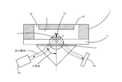
- FIG. 23 is a diagram for explaining the configuration of the SPR sensor proposed by Kretschmann.
- the SPR sensor main body has a structure in which a metal thin film 4 is provided on a prism 8 made of glass having a refractive index higher than that in the atmosphere. Then, monochromatic light such as laser light is incident on the boundary surface between the prism 8 and the metal thin film 4. The incident angle of light is set to an angle greater than the critical angle at which total reflection occurs at the boundary surface. The monochromatic light is totally reflected at the boundary surface and travels out of the prism 8. At this time, the evanescent wave oozes out to the surface of the metal thin film 4.
- SPR sensors are used for various measurements. For example, as described in Patent Document 1 (Japanese Patent Application Laid-Open No. 6-167443), the SPR sensor is used as a microscope for measuring information near the surface of a dielectric material and the film thickness distribution of the dielectric thin film with high sensitivity. Is done.
- the SPR sensor measures the refractive index of a solution (for example, a sample of blood, urine, etc.) in contact with a metal thin film and its variation. Detects and observes changes in the amount of substances in the solution, and detects and quantifies proteins, nucleic acids, other biologically related substances, etc. that bind specifically to the antibody immobilized on the metal thin film (monitors antibody antigen reaction) ) Is also used. That is, the SPR sensor is used as a biosensor used in fields such as biochemistry, molecular biology, and medical examination.
- FIG. 24 shows a configuration example of a microchip and an SPR sensor using the microchip.
- a microchip used as an object to be inspected of an SPR sensor typically has a structure in which a pair of substrates (a first microchip substrate 1 and a second microchip substrate 2) are bonded to each other.
- a fine flow path 3 (microchannel: for example, a width of about 10 to several hundred ⁇ m and a depth of about 10 to several hundred ⁇ m) is formed on the surface of at least one of the substrates.
- a metal thin film 4 is applied to the second microchip substrate 2, and an antibody Ig (antigen receptor) is immobilized on the metal thin film 4.
- the flow path 3 is formed in the first microchip substrate 1.
- the metal thin film 4 and the antibody Ig fixed to the metal thin film 4 are in the flow path 3.
- the specimen containing the antigen is introduced from the inlet 3a of the flow path 3 and discharged from the outlet 3b.
- the metal thin film 4 is provided on the prism 8 made of glass having a refractive index higher than that in the atmosphere. Therefore, originally, the second microchip substrate 2 in FIG. 24 needs to be a prism 8 as shown in FIG. However, in this case, it is necessary to prepare the prism 8 for each microchip, which increases the cost.
- the second microchip substrate 2 is a glass substrate made of the same material as the prism 8, and the matching oil which is a medium having a refractive index substantially the same as that of the glass between the second microchip substrate 2 and the prism 8. 7 is interposed.
- the microchip and the prism 8 are optically bonded. According to this configuration, it is not necessary to prepare the prism 8 for each microchip, and when performing a plurality of measurements, it is only necessary to replace the microchip.
- the light source 6a for irradiating the metal thin film 4 with light is, for example, a semiconductor laser device, and a laser beam with a wavelength of 670 nm, for example, is emitted.
- Light irradiation from the light source 6a is controlled by a control unit (not shown).
- the laser beam emitted from the light source 6a passes through a polarizing element (not shown) and then becomes a P-polarized laser beam and is applied to the metal thin film 4.
- the reflected light from the metal thin film 4 is received by the CCD 6b (solid-state imaging device).
- the image information from the CCD 6b is sent to a control unit (not shown), and the control unit that receives the image information from the CCD 6b analyzes the image information and monitors the antibody-antigen reaction.
- the metal thin film 4 is an enlarged cross-sectional view of a portion A in FIG.
- Silver, gold, copper, aluminum, or the like is used as the metal thin film 4 that exhibits surface plasmon resonance (SPR).
- SPR surface plasmon resonance
- Au gold
- the thickness of the gold film 4a is, for example, 20 to 50 nm.
- a buffer layer 4c as described in JP 2002-257720 A) is provided.
- a titanium (Ti) film is provided as the buffer layer 4c.
- the thickness of the titanium film 4c is, for example, 3 to 5 nm.
- an ultrathin titanium oxide (TiO2) film 4b in which the surface of the titanium film is oxidized by oxygen in the atmosphere exists between the titanium film 4c and the gold film 4a.
- the metal thin film 4 shown in FIG. 25 is constructed by the following processes, for example. First, a titanium film is provided on the second microchip substrate 2 which is a glass substrate by vapor deposition or sputtering. Next, a gold film 4a having a thickness of 20 to 50 nm is formed on the titanium film by vapor deposition or sputtering. In addition, after forming the titanium film 4c on the second microchip substrate 2 and forming the gold film 4a on the titanium film 4c, the second microchip substrate 2 on which the titanium film 4c is formed is exposed to air. Often exposed. Therefore, before forming the gold film 4a on the titanium film 4c, the titanium oxide film 4b which is a natural oxide film is formed on the surface of the titanium film 4c.
- the titanium oxide film 4b is interposed between the titanium film 4c and the gold film 4a. Since the titanium oxide film 4b exhibits high hydrophilicity, it is considered that the metal thin film 4 such as gold can be closely adhered to the surface of the titanium oxide film 4b.
- the titanium (Ti) film 4c serving as a buffer layer is useful as an adhesive layer for improving the adhesion between the second microchip substrate 2 serving as a glass substrate and the gold (Au) film 4a, but has a light extinction coefficient. large.
- the extinction coefficient of the titanium film 4c with respect to incident light having a wavelength of 670 nm is as large as 3.65. Therefore, for example, even if the thickness of the titanium film 4c varies by 1 nm, the reflected light (that is, the SPR signal) of the light irradiated on the back surface of the metal thin film 4 changes greatly.
- the thickness of the titanium film 4c it is necessary to control the thickness of the titanium film 4c to be uniform among the individuals.
- the vapor deposition method and the sputtering method for forming the titanium film 4c it has been difficult to control the film thickness deviation to be smaller than 1 nm.
- the buffer layer has a small extinction coefficient while improving the adhesion between the glass substrate (second microchip substrate 2) and the SPR metal thin film such as an Au film. Is required.
- TiO 2 titanium oxide
- Au gold
- a titanium oxide film generally has a high transmittance in the visible region and a small extinction coefficient in the visible region. Moreover, it is chemically stable and the surface is hydrophilic. Therefore, the titanium oxide film has good adhesion to the gold film and is useful as an adhesive layer that improves the adhesion between the second microchip substrate, which is a glass substrate, and the gold film.
- the titanium oxide film since the titanium oxide film has a smaller extinction coefficient in the visible region than the titanium film, the influence of the deviation of the thickness of the titanium oxide film on the SPR signal is small. Therefore, the uniformity of the thickness of the titanium oxide film may not be as high as the deviation of about 1 nm as in the case of the titanium film.
- a titanium oxide film as a metal thin film buffer layer is formed on a glass substrate using a conventional titanium oxide film forming method, there are the following problems.
- a titanium oxide film is formed on a substrate surface by using a titanium oxide sol obtained by dispersing titanium oxide powder or fine titanium oxide particles of about 10 nm in water or a solvent, or a titania sol in which a titanium compound such as titanium alkoxide is dissolved. For example, and sintering at a temperature of about 600 ° C. or less.
- Application of titanium oxide sol or titania sol to the surface of the substrate is performed, for example, by spraying them onto the surface of the substrate with a spray or the like.
- Patent Document 4 Japanese Patent Laid-Open No. 2001-262008.
- the titanium oxide film is fixed by physical adsorption. Therefore, the physical strength of the titanium oxide film on the surface of the glass substrate varies depending on the thickness of the titanium oxide film. That is, when the titanium oxide film is formed relatively thick on the glass substrate, the titanium oxide film is easily peeled off.
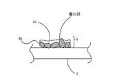
- the titanium oxide film fixed on the surface of the glass substrate as described above generally has an amorphous structure, is close to an anatase structure, and has a particulate shape as shown in FIG. Therefore, even when the gold film 4a is formed on the titanium oxide film 4b by vapor deposition or sputtering, the bonding state between the titanium oxide film 4b and the gold film 4a is weak. Further, the titanium oxide film 4b having the anatase structure may be exposed from the gold film 4a in some places. In such a case, even if an organic substance such as a protein is immobilized on the gold film 4a, at least a part of the immobilized protein is decomposed by the photocatalytic reaction of titanium oxide.
- the subject is a microchip by which metal thin films, such as gold
- a titanium oxide film can be easily formed on the surface of the glass substrate, and the thickness of the titanium oxide film can be controlled. It is an object of the present invention to provide a method for forming a metal thin film on a glass substrate of a microchip that is possible.
- the microchip of the present invention has a pair of substrates (first microchip substrate 1 and second microchip substrate as shown in FIG. 1A). 2) have a structure in which they are bonded to each other, and a fine channel 3 (microchannel: for example, a width of about 10 to several hundred ⁇ m and a depth of about 10 to several hundred ⁇ m) is formed on the surface of at least one of the substrates. ing.
- a metal thin film 4 is applied to the second microchip substrate 2, and an antibody (antigen receptor) is immobilized on the metal thin film 4.
- the flow path 3 is formed in, for example, the first microchip substrate 1.
- the first microchip substrate 1 is made of, for example, a silicone resin such as polydimethylsiloxane (PDMS).
- PDMS polydimethylsiloxane
- the specimen containing the antigen is introduced from the inlet 3a of the flow path 3 and discharged from the outlet 3b.
- chemically stable gold Au
- the thickness of the Au film 4a is, for example, 20 to 50 nm.
- titanium oxide TiO2
- a film 4b is provided.
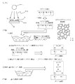
- a titanium oxide film can be formed on a glass substrate by performing the following steps 0 to 3 shown in FIG. 2 on the substrate which is a molded body made of glass.
- Step 0 Ultraviolet light is irradiated from the light source L onto the surface of the base material W (second microchip substrate 2), which is a molded body made of glass that fixes titanium oxide in an air atmosphere containing oxygen and moisture.
- the metal thin film 4 is formed on a part of the base material W (second microchip substrate 2) made of glass, the titanium oxide film is also actually formed on a part of the base material W. For this reason, as shown in FIG. 2, the shielding member 5 which has the opening 5a corresponding to the formation area of the titanium oxide film is provided on the surface of the base material W.
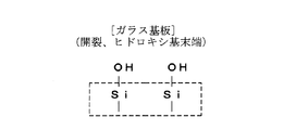
- the siloxane bond portion on the glass surface is cleaved as shown in Step 0 of FIG.
- Oxygen (O) combined with is exposed on the glass surface.
- This exposed oxygen is combined with water hydrogen (H) contained in the atmosphere to form a hydroxy group. That is, the end of the glass surface is ultimately considered to be a hydroxy group.
- the glass has an amorphous structure as shown in FIG. 2, and silicon and oxygen are irregularly arranged.
- the surface structure of the glass is linearly arranged with silicon and oxygen. Shown as a siloxane structure.
- skeleton was taken as an example as glass, it is not restricted to this.
- oxide glass such as borate glass may be used, and even in such glass, it is considered that the end of the glass surface becomes a hydroxy group as a result of step 0.
- vacuum ultraviolet light including light having a wavelength of 200 nm or less (preferably light having a wavelength of 180 nm or less) that is absorbed by the glass and exceeds the activation energy of the glass is the above-mentioned Irradiate the surface.
- the surface may be irradiated with monochromatic light having a center wavelength at a wavelength of 172 nm emitted from a vacuum ultraviolet excimer lamp.
- Process 1 (Process 1) The said base material is immersed in the liquid mixture of titanium chloride aqueous solution and nitrite ion containing aqueous solution (for example, sodium nitrite aqueous solution) (process 1 (a) of FIG. 2). As a result of the immersion, as shown in step 1 (b) of FIG. 2, hydrogen is released from the hydroxyl group terminal of the base material made of glass, and oxygen and titanium ions in the mixed solution are bonded.
- aqueous solution for example, sodium nitrite aqueous solution
- the oxidation of titanium ions by nitrite ions, the bond between oxidized titanium ions and oxygen, and the bond between bonded oxygen and titanium ions are repeated, and from the glass A titanium oxide film grows on the ultraviolet light irradiation surface of the substrate to be formed (step 1 (c) in FIG. 2).
- Step 2 After a predetermined time has elapsed, as shown in step 2 of FIG. That is, the reaction is stopped by washing with pure water. As the immersion time elapses, the thickness of the titanium oxide film on the base material increases, but the formation reaction of the titanium oxide film stops by lifting the base material from the mixed solution and washing it. It is considered that the film thickness of the titanium oxide film can be controlled by controlling the immersion time.
- Step 3 The substrate after washing is dried at room temperature.
- Step 4 Through steps 0 to 3, the titanium oxide film 4b is formed on a part of the base material W (the second microchip substrate 2 that is a glass substrate) (the portion of the opening 5a of the shielding member 5). . Subsequently, the base material W that has undergone the process 3 is placed in a film forming apparatus that realizes film formation by vapor deposition, sputtering, or the like, and gold (Au) is disposed on the shielding member side of the base material W as shown in FIG. A film 4a is formed. (Step 5) After forming the gold (Au) film in step 4, the shielding member 5 is peeled from the second microchip substrate 2 (base material W) as shown in FIG.
- the Au film 4a is removed from the second microchip substrate 2 together with the shielding member 5 except for the film formed on the titanium oxide film 4b.
- Step 6 As shown in FIG. 3, the first microchip substrate 1 is laminated on the second microchip substrate 2 and bonded.
- a microchip with the metal thin film 4 applied in the flow path 3 is formed. That is, in an aspect of the present invention, the above-described problem is solved as follows. (1) In a microchip including a substrate made of glass on which a metal thin film is formed, and a flow path is formed in a space including the metal thin film, one surface is between the substrate and the metal thin film. A titanium oxide film in contact with the metal thin film is provided on the other surface.
- a metal thin film having a titanium oxide film provided between the substrate and the substrate is formed as follows.
- a shielding member having an opening corresponding to the size of the metal thin film to be deposited is installed on the surface of the substrate made of glass, and the surface of the substrate on the shielding member side in an air atmosphere containing oxygen and moisture.
- Irradiate light including vacuum ultraviolet light having a wavelength of 200 nm or less, immerse the substrate in a mixed solution of a titanium chloride aqueous solution and a nitrite ion-containing aqueous solution, immerse the substrate in the mixed solution, and after a predetermined time has elapsed, The substrate is lifted from the mixed solution, washed with water to stop the film formation process, and the substrate after washing with water is dried at room temperature.
- a metal thin film is deposited on the shielding member side surface of the substrate.
- the shielding member is removed from the substrate.
- the metal thin film is any one of gold (Au), platinum (Pt), rhodium (Rh), palladium (Pd), and palladium-platinum alloy (Pd—Pt alloy). You may comprise.
- the microchip of the present invention employs a titanium oxide film having a small extinction coefficient as a buffer film for a metal thin film applied on a substrate made of glass. Accordingly, the influence of the deviation of the buffer film thickness on the SPR signal is small. Therefore, the uniformity of the thickness of the titanium oxide film may not be as high as the deviation of about 1 nm as in the case of the titanium film.
- the titanium oxide film has a hydrophilic surface, has good adhesion to a metal thin film such as gold, and is useful as an adhesive layer that improves the adhesion between the glass substrate and the metal thin film.
- the substrate surface made of glass is irradiated with light containing ultraviolet light having a wavelength of 200 nm or less through a shielding member having an opening, and then the base material contains an aqueous titanium chloride solution and nitrite ions. Since the titanium oxide film is formed on the substrate surface made of glass by immersing the base material in the mixed solution of the aqueous solution, the baking step of heating to several hundred degrees for crystallizing the titanium oxide on the base material do not need. Therefore, titanium oxide particles are not generated by the heating process. For this reason, the bonding state between the titanium oxide film and the gold film is good, and the titanium oxide film is not exposed from the gold film in some places. (4) Since the titanium oxide film thickness on the substrate increases with the lapse of the immersion time, the titanium oxide film thickness can be easily controlled by controlling the immersion time.
- the titanium oxide film formation according to the present invention is formed by chemical bonding on the glass substrate, the physical strength of the titanium oxide film on the surface of the glass substrate is equal to the film thickness of the titanium oxide film. Is not dependent. That is, it is possible to form a titanium oxide film that is firmly bonded to the glass substrate.
- the titanium oxide is not formed using the hydrolysis reaction, it is not necessary to set the solution temperature to a temperature higher than the normal temperature.
- the titanium oxide film formed according to the present invention has the property of rutile-type high transparency as well as the photocatalytic function of the anatase-type titanium oxide film, and the titanium oxide film formed on the glass substrate according to the present invention The extinction coefficient is small. Therefore, the influence of the thickness deviation of the titanium oxide film on the SPR signal is small.
- the titanium oxide film formed according to the present invention has a hydrophilic surface, when a gold film is formed on such titanium oxide by vapor deposition or sputtering, the titanium oxide film and the gold film are bonded. The state is strong.
- FIG. 1A is a diagram illustrating a configuration example of a microchip according to an embodiment of the present invention.
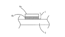
- FIG. 1B is a diagram illustrating a configuration example of the metal thin film 4 of FIG. 1A.
- FIG. 2 is a schematic diagram for explaining the outline of the process of forming a titanium oxide film on a substrate made of glass, for example, in the embodiment of the present invention.
- FIG. 3 illustrates a process of forming a metal thin film having a titanium oxide film as shown in FIG. 2 and joining the first and second microchip substrates to form the microchip according to the embodiment of the present invention. It is a schematic diagram.
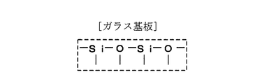
- FIG. 4A is a diagram illustrating an initial state of the glass substrate in step 0 of FIG. FIG.
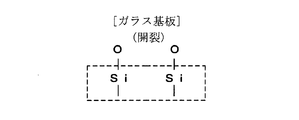
- FIG. 4B is a diagram illustrating the cleavage of the olefin ring of the glass substrate in step 0 of FIG.
- FIG. 4C is a diagram illustrating oxygen introduction into the olefin ring of the glass substrate in step 0 of FIG.
- FIG. 5 is a diagram (1) illustrating the formation of a titanium oxide film in step 1 of FIG.
- FIG. 6 is a diagram (2) illustrating the formation of a titanium oxide film in step 1 of FIG.
- FIG. 7 is a diagram (3) for explaining the formation of the titanium oxide film in step 1 of FIG.
- FIG. 8 is a diagram (4) illustrating the formation of a titanium oxide film in step 1 of FIG.
- FIG. 9 is a diagram (5) for explaining the formation of the titanium oxide film in step 1 of FIG. FIG.
- FIG. 10 is a diagram (6) illustrating the formation of the titanium oxide film in step 1 of FIG.
- FIG. 11 is a diagram (7) illustrating the formation of a titanium oxide film in step 1 of FIG.
- FIG. 12 is a view (8) illustrating the formation of the titanium oxide film in step 1 of FIG.
- FIG. 13A is a diagram for explaining light irradiation to the bonding surface of the first microchip substrate in the step of bonding the first and second microchip substrates.
- FIG. 13B is a diagram for explaining the step of bonding the first microchip substrate of FIG.
- FIG. 13C is a diagram illustrating a configuration of a microchip obtained by the bonding process of FIGS. 13A and 13B.
- FIG. 14 is a diagram illustrating a configuration example of an excimer lamp.
- FIG. 14 is a diagram illustrating a configuration example of an excimer lamp.
- FIG. 15 is a diagram showing the distribution of the emission wavelength of the excimer lamp.
- FIG. 16 is a schematic diagram of an experimental system in which the substrate is irradiated with vacuum ultraviolet light from an excimer lamp.
- FIG. 17 is a view showing that wettability is improved by irradiating glass with ultraviolet rays.
- FIG. 18 is a diagram showing XPS measurement results relating to titanium oxide of a sample that has been subjected to the processes of Step 0 to Step 3 of FIG. 2 using three kinds of mixed liquids.
- FIG. 19A is a side view showing another configuration example of the rare gas fluorescent lamp.
- FIG. 19B is an enlarged sectional view taken along line 19A-19A in FIG. 19A.
- FIG. 19A is a side view showing another configuration example of the rare gas fluorescent lamp.
- FIG. 20 is a diagram illustrating an example of the extinction coefficient of the titanium film and the titanium oxide film with respect to the incident light wavelength.
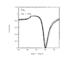
- FIG. 21 is a diagram showing an example of the change of the SPR signal with respect to the thickness of the titanium oxide film.
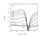
- FIG. 22 is a diagram showing an example of the change of the SPR signal with respect to the thickness of the titanium film.
- FIG. 23 is a schematic diagram illustrating an SPR sensor.
- FIG. 24 is a diagram illustrating a configuration example of a microchip and an SPR sensor using the microchip.
- FIG. 25 is a diagram showing a configuration example of a metal thin film having a titanium film.
- FIG. 26 is a schematic diagram for explaining a case where the titanium oxide film fixed on the surface of the glass substrate has a particulate shape.
- Step 0 Processing in each step in the embodiment of the present invention will be described.
- the following steps 0 to 3 are performed on the second microchip substrate 2 made of glass, and a titanium oxide film is formed on a part of the second microchip substrate 2 made of glass.
- a shielding member 5 On one surface of the second microchip substrate 2, a shielding member 5 having an opening 5a corresponding to a region where a titanium oxide film is to be formed is provided as shown in FIG.
- the surface of the second microchip substrate 2 made of glass for fixing titanium oxide under an atmosphere is irradiated with ultraviolet light.
- Step 1 The second microchip substrate 2 is immersed in a mixed solution of a titanium chloride aqueous solution and a nitrite ion-containing aqueous solution (for example, a sodium nitrite aqueous solution).
- Step 2 After a predetermined time has elapsed, the second microchip substrate 2 is pulled up from the mixed solution and washed with pure water (this stops the reaction).
- Step 3 The substrate after cleaning is dried at room temperature.
- the second microchip substrate 2 is irradiated with ultraviolet light in an air atmosphere containing oxygen through a shielding member having an opening corresponding to the region where the titanium oxide film is formed.
- the above-described shielding member is a stencil having an opening made of, for example, silicone or stainless steel. This shielding member is arranged and fixed on one surface of the second microchip substrate 2 with a holder or the like not shown.
- the process 0 adopted in the present embodiment exerts the following action on the second microchip substrate 2 made of glass (hereinafter also referred to as a glass molded body).
- a glass molded body By irradiating the surface of the second microchip substrate 2 (glass molded body) made of ultraviolet glass, the surface of the molded body is activated. Specifically, cleavage of the bonded portion between metal atoms and oxygen on the surface of the molded body occurs. For example, in the case of a general silicate glass, cleavage of the siloxane bond portion occurs.
- the activated surface of the molded body is bonded to hydrogen in the atmosphere, and the glass surface becomes a hydroxyl group terminal. That is, oxygen (O) is exposed on the glass surface by the above cleavage. This exposed oxygen is combined with water hydrogen (H) contained in the atmosphere to form a hydroxy group. That is, the end of the glass surface is ultimately considered to be a hydroxy group. And it was confirmed that the titanium oxide film
- a heating procedure is not required but it implements at normal temperature.
- the incidental effect that dirt such as organic substances adhering to the glass surface is decomposed is also remarkably obtained when the vacuum ultraviolet light having a wavelength of 180 nm or less is irradiated. Since dirt such as organic matter may become a reaction inhibitor for the formation reaction of the titanium oxide film in step 1 to be described later, in step 0, it is particularly preferable to irradiate vacuum ultraviolet light having a wavelength of 180 nm or less.
- the mechanism by which titanium oxide is fixed to the second microchip substrate 2 (glass molded body) made of glass by the method for forming a titanium oxide film on the substrate of the present embodiment is considered as follows.
- 4A, FIG. 4B, and FIG. 4C illustrate the cleavage of the bonded portion of the metal atom and the like and oxygen in Step 0 and the termination of the hydroxy group.
- silicate glass having a silicon dioxide skeleton was taken as an example of glass, but the glass is not limited thereto.
- step 0 the glass molded body is irradiated with light containing ultraviolet light having a wavelength of 200 nm or less (specifically, vacuum ultraviolet light having a wavelength of 180 nm or less (also referred to as vacuum ultra violet: VUV)) (FIG. 4A ⁇ FIG. 4B).
- VUV vacuum ultra violet
- FIG. 4B cleavage of the bonded portion of the metal atom or the like (silicon: Si in the examples of FIGS. 4A, 4B, and 4C) and oxygen (O) occurs.
- FIG. 4C hydrogen is introduced from the moisture in the atmosphere into the cleaved portion, and it is considered that the terminal of the glass surface eventually becomes a hydroxy group.
- step 1 of FIG. 2 the glass molded body irradiated with VUV is divided into a titanium (III) chloride aqueous solution (TiCl 3 aqueous solution) and a sodium nitrite aqueous solution (NaNO 2 aqueous solution). Immerse in the mixture.
- the mixed liquid contains titanium ions (Ti 3+ ) and nitrite ions (NO 2 ⁇ ).
- step (b) of FIG. 5 hydrogen is released from the hydroxyl group terminal of the glass molded body, and oxygen and titanium ions in the mixed solution are bonded.
- the silicon dioxide forming the glass is considered to have a crystal structure such as quartz.
- (M-0) and (m-1) in FIG. 5 are schematic views in which oxygen and titanium ions are bonded in the crystal structure.
- the hatched circle in the figure is a titanium atom (ion).
- a transparent (rutile-type) titanium oxide film was formed on the glass surface by performing the processes of Step 0 to Step 3. From this experimental result, as shown in the schematic diagram of (m-1) in FIG. 5, it is considered that the titanium molecules bonded to oxygen are distributed so as to be arranged in a quadrangular shape. In other words, the distribution of the hydroxyl group terminals exposed on the glass surface due to cleavage of silicon (Si) and oxygen (O) bonds by VUV irradiation corresponds to the distribution of oxygen atoms exposed on the glass surface in the mixed solution. . Since titanium ions are bonded to the exposed oxygen atoms, the arrangement of the titanium ions depends on the distribution of oxygen atoms described above.
- the distribution of titanium ions bonded to oxygen is a distribution corresponding to the bonding distance of titanium oxide, and the arrangement of titanium is a distribution that forms a rutile tetragonal system. That is, the molecular structure of the titanium oxide film formed by the method for forming a titanium oxide film of this embodiment is predominantly rutile.
- a cubic first stage is formed by four titanium atoms. Two oxygen atoms are distributed in a quadrangle composed of four titanium atoms.
- step (c) of FIG. 6 [(titanium oxidation) ⁇ (bonding of titanium and oxygen)] is repeated.
- step (c-1) of FIG. 6 titanium ions bonded to oxygen of the glass molded body and nitrite ions coexisting with titanium ions in the mixed solution are oxidized to become Ti3 + ⁇ Ti4 +. (Refer to the schematic diagram (m-2) in FIG. 6).
- the oxidized titanium ions are combined with oxygen donated from the water in the mixed solution as shown in step (c-2) in FIG.
- the first stage of a quadrilateral crystal composed of four titanium atoms (titanium ions) and two oxygen atoms distributed in the quadrilateral shown in the schematic diagram (m-3) of FIG. I will call it eyes.
- the bond between titanium ions and oxygen atoms in step (c-2) in FIG. 7 is one in which one oxygen atom is bonded to two titanium ions in the first layer. Since there are four titanium ions in the first layer, the number of oxygen atoms to be bonded is two. A region where two oxygen atoms are located is referred to as a second layer for convenience as shown in FIG. 7 (m-3).
- step (c-3) in FIG. 8 the oxygen atoms and titanium ions in the mixed solution are bonded.
- step (m-4) of FIG. 8 two oxygen atoms located in the first layer are bonded to one titanium ion.
- step (c-1) in FIG. 9 and the schematic diagram (m-5) in FIG. 9 one titanium ion introduced as described above is oxidized by nitrite ions, and Ti3 + ⁇ Ti4 +.
- the oxidized titanium ions are combined with oxygen donated from moisture in the mixed solution as shown in step (c-2) in FIG.
- two oxygen atoms are bonded to one titanium ion in the second layer.
- the region where the two oxygen atoms are located will be referred to as the third layer.
- the oxygen atoms and titanium ions in the mixed solution are bonded.
- two oxygen atoms in the third layer are bonded to four titanium ions.
- four titanium ions are oxidized by the nitrite ions.
- Step 1 (c-1) oxidation of titanium ions by nitrite ions and (c-2) oxidized titanium ions and oxygen at the olefin ring cleavage ends of the cyclic olefin-based molded body. (C-3) Bonding of bonded oxygen and titanium ions is repeated, and it is considered that a titanium oxide film grows on the VUV irradiated surface of the glass molded body.
- titanium oxide is expressed by the following reaction formula. It is thought that is formed. 3Ti +3 + 6H 2 O ⁇ 3TiO 2 + 12H + + 3e ⁇
- the formation of the titanium oxide film in step 1 described with reference to FIGS. 5 to 12 is based on the assumption that the silicon dioxide forming the glass (silicate glass) has a crystal structure such as quartz as described above. It is. Actually, as shown in FIGS. 1A and 1B, glass has an amorphous structure, and silicon and oxygen are irregularly arranged.
- the crystal structure of titanium oxide formed on the glass molded body is considered to be determined by the position of oxygen present on the surface of the glass molded body. Therefore, when the silicon dioxide forming the glass (silicate glass) has a crystal structure like a crystal, the distribution of titanium ions bonded to oxygen atoms exposed on the surface indicates that the crystal structure of the growing titanium oxide film is a rutile type.
- the arrangement of oxygen atoms exposed to the glass surface in step 0 that is, the distribution of titanium ions bonded to oxygen
- the distribution of the crystal structure of the titanium film is not a rutile tetragonal system.
- Anatase-type titanium oxide is formed in a region where the arrangement of oxygen atoms exposed on the surface is substantially the same as the lattice constant of anatase-type titanium oxide when the arrangement (distance) of titanium ions bonded to the oxygen atom is the same. It is considered a thing. That is, it is considered that the rutile type titanium oxide and the anatase type titanium oxide are mixed in the titanium oxide film formed on the surface of the amorphous glass molded body.
- step 2 After immersing the glass molded body in the mixed solution for a predetermined time as described above, in step 2, the glass molded body is pulled up from the mixed solution and washed with pure water or the like to stop the reaction.
- the thickness of the titanium oxide film on the substrate increases with the elapse of the immersion time in the above mixed solution, but the formation reaction of the titanium oxide film stops by lifting the substrate from the mixed solution and washing, and this immersion time is reduced. It is considered that the thickness of the titanium oxide film can be controlled by controlling.
- step 3 the washed substrate is dried at room temperature.
- Step 4 to Step 5 the following steps 4 and 5 are performed on the second microchip substrate 2 that has undergone the above-described steps 0 to 3, as shown in FIG.
- a metal foil film such as gold (Au) is formed on the titanium oxide film formed on a part of the microchip substrate 2.
- the second microchip substrate (glass molded body) made of glass that has undergone the process 3 is placed in a film forming apparatus that realizes film formation by vapor deposition or sputtering, and the glass molded body side of the shielding member Then, a metal thin film such as gold (Au) is formed.
- the shielding member is peeled from the second microchip substrate. As a result of the peeling, the Au film is removed from the second microchip substrate together with the shielding member except for the film formed on the titanium oxide film.
- the metal thin film 4 is formed on the shielding member side of the glass molded body that has undergone step 3.
- gold, silver, copper, aluminum, or the like is used as a metal material for forming a metal thin film, but it corresponds to visible light or near infrared light, and is a chemically stable metal material.
- gold (Au) is used.
- metal materials other than gold having the same effect as gold include platinum (Pt) and rhodium (Rh).
- step 5 by removing the shielding member from the second microchip substrate, the metal thin film such as Au is removed from the second microchip substrate together with the shielding member except for the one formed on the titanium oxide film. The The removal of the shielding member is performed, for example, by removing the holder (not shown) and removing it from the second microchip substrate 2.
- Step 6 the following step 6 is performed on the second microchip substrate that has undergone the above-described steps 0 to 5, and a microchip that includes the second microchip substrate and the first microchip substrate.
- the first microchip substrate is stacked on the second microchip substrate and bonded.
- the bonding of the microchip substrate is performed by applying a vacuum to the surface of the first microchip substrate 1 as shown in, for example, Patent Document 5 (Japanese Patent Laid-Open No. 2006-187730) and Patent Document 6 (Japanese Patent No. 3714338). After the surface is activated by irradiating with ultraviolet light, the second microchip substrate 2 is bonded together.
- the first microchip substrate 1 is irradiated with light from an excimer lamp having an emission line at a wavelength of 172 nm to perform a modification process (oxidation process) on the surface.
- the modified side of the first microchip substrate 1 and the surface of the second microchip substrate 2 on which the metal thin film 4 is applied are opposed to each other. Are stacked and adhered to form a microchip as shown in FIG. 13C.
- the microchip of this embodiment employs a titanium oxide film having a small extinction coefficient as a buffer film for a metal thin film applied on the second microchip substrate 2. Accordingly, the influence of the deviation of the buffer film thickness on the SPR signal is small. Therefore, the uniformity of the thickness of the titanium oxide film may not be as high as the deviation of about 1 nm as in the case of the titanium film.
- the titanium oxide film has a hydrophilic surface, has good adhesion to a metal thin film such as gold, and improves the adhesion between the second microchip substrate 2 which is a glass substrate and the metal thin film 4. It is useful as an adhesive layer.
- the titanium oxide film formed of the titanium oxide film of the present invention has a hydrophilic surface, when the gold film 4a is formed on such titanium oxide by vapor deposition or sputtering, the titanium oxide film and the gold The bonding state with the film 4a is strong.
- the film thickness of the gold film 4a is also relatively uniform.
- the formation of the titanium oxide film on the second microchip substrate 2 in this embodiment is performed by oxidizing titanium (c-1), oxidized titanium and oxygen. (C-2), and the bond between oxygen and titanium (c-3) is repeatedly performed. That is, as the immersion time elapses, the thickness of the titanium oxide film on the substrate increases, so that the titanium oxide film thickness can be easily controlled by controlling the immersion time. That is, the film thickness of the titanium oxide film is controlled by washing the surface with water as in step 2 to stop the titanium oxide film formation reaction.
- the titanium oxide is not formed using the hydrolysis reaction, it is not necessary to set the solution temperature to a temperature higher than the room temperature.
- the titanium oxide film formed according to this embodiment grows by a covalent bond between oxygen and titanium ions on the glass surface, the titanium oxide is fixed to the glass surface by physical adsorption using a conventional wet process. In contrast, even if the titanium oxide film is formed relatively thick, it is firmly fixed to the glass surface.
- the baking process heated to several hundred degrees for crystallizing a titanium oxide on a base material is not required. Therefore, titanium oxide particles are not generated by the heating process. Therefore, there is no problem that the titanium oxide film is exposed from the metal thin film 4 such as the gold film 4a.
- Steps 1, 2, and 3 for sequentially immersing the substrate in the mixed solution, elevating the substrate from the mixed solution after a predetermined time, washing, and drying the washed substrate at room temperature will be sequentially described.
- Step 0 is a step of providing the shielding member 5 having the opening 5a on the surface of the glass molded body (base material W) as shown in FIG. 2 and irradiating the surface of the glass molded body on the shielding member side with ultraviolet light.
- the above-described shielding member 5 is a stencil having an opening 5a made of, for example, silicone or stainless steel.
- the shielding member 5 is arranged and fixed on one surface of the second microchip substrate 2 with a holder or the like not shown.
- FIG. 14 is a diagram illustrating a configuration example of an excimer lamp.
- the excimer lamp has a tubular structure, and FIG. 14 shows a cross-sectional view taken along a plane including the tube axis.
- the excimer lamp 10 has a container (light emitting tube) 11 having a substantially double tube structure in which an inner tube 111 and an outer tube 112 are arranged substantially coaxially, and both end portions 11A and 11B of the container 11 are sealed.
- a cylindrical discharge space S is formed inside.
- the discharge space S is filled with a rare gas such as xenon, argon, or krypton.
- the container 11 is made of quartz glass.
- An inner electrode 12 is provided on the inner peripheral surface of the inner tube 111, and a net-like outer electrode 13 is provided on the outer peripheral surface of the outer tube 112. These electrodes 12 and 13 are disposed with the container 11 and the discharge space S interposed therebetween.
- the electrodes 12 and 13 are connected to the power supply device 16 via lead wires W11 and W12.
- a discharge sin-called dielectric barrier discharge
- dielectrics 111, 112
- a center wavelength of 172 nm is formed. Vacuum ultraviolet light is generated, and the vacuum ultraviolet light is emitted to the outside.
- FIG. 15 shows an example of a radiation wavelength distribution when the excimer lamp 10 shown in FIG. 14 is lit at a frequency of 20 KHz and a tube wall load of 0.1 W / cm 2.
- the horizontal axis represents the emission wavelength
- the vertical axis represents the relative value with respect to the intensity of light having a wavelength of 170 nm.
- FIG. 16 shows a schematic diagram of the experimental system. As shown in FIG. 16, the substrate W on the work stage WS was irradiated with vacuum ultraviolet light from the excimer lamp 10. As the excimer lamp 10, an excimer lamp that emits vacuum ultraviolet light having a center wavelength of 172 nm as described above was used, and the irradiance on the sample surface was 20 mW / cm 2.
- FIG. 17 is a diagram showing an example of how wettability is improved when ultraviolet rays are irradiated on glass.
- the horizontal axis in FIG. 17 is the ultraviolet irradiation time (sec)
- the vertical axis is the contact angle of water with respect to glass (°)
- FIG. 17 is a graph showing a standard output excimer lamp (10 mW / cm 2) with an irradiation distance of 2 mm. Data when irradiated with ultraviolet rays of 172 nm is shown. As shown in FIG.
- the contact angle (°) of water with respect to the glass is reduced by irradiating the glass with ultraviolet rays, and the wettability is improved. It is considered that the wettability is improved by irradiating the glass with ultraviolet rays, whereby the glass surface is activated and the terminal of the activated surface is a hydroxy group (OH group).
- the surface treatment of the glass molded body by the step 0 of irradiating the surface of the glass molded body with ultraviolet light activates the surface and the end of the activated surface becomes a hydroxy group.
- the activation of the surface is performed by cleaving the bonded portion between the metal atom and the oxygen on the surface and the moisture in the atmosphere at the cleaved portion. From this, hydrogen is introduced, and it is thought that the terminal of the glass surface eventually becomes a hydroxy group.
- Step 1 is a step of immersing a base material, which is a glass molded body having a surface irradiated with ultraviolet light (vacuum ultraviolet light) in Step 0, in a mixed solution of a titanium chloride aqueous solution and a nitrite ion-containing aqueous solution. Is to wash the substrate from the mixed solution after a predetermined time has elapsed, and in step 3, the washed substrate is dried at room temperature.
- a base material which is a glass molded body having a surface irradiated with ultraviolet light (vacuum ultraviolet light) in Step 0
- a mixed solution of a titanium chloride aqueous solution and a nitrite ion-containing aqueous solution Is to wash the substrate from the mixed solution after a predetermined time has elapsed, and in step 3, the washed substrate is dried at room temperature.
- the used base material is a molded body formed using silicate glass, and the shape thereof is a square substrate having a thickness of 2 mm, a length of 8 mm, and a width of 8 mm.
- This substrate was irradiated with vacuum ultraviolet light from an excimer lamp that emits vacuum ultraviolet light having a center wavelength of 172 nm for 1 to 2 minutes.
- the irradiance on the substrate irradiated surface was 4 to 5 mW / cm 2 or less.
- Step 1 Step 2 and Step 3
- a titanium (III) chloride aqueous solution having a titanium chloride (III) concentration of 20% to 10 mM and a sodium nitrite aqueous solution having a sodium nitrite concentration of 0.1 M The substrate was immersed in the liquid.
- XPS measurement of the surface was performed using an XPS-7000 type X-ray electron spectrometer (XPS) apparatus manufactured by Rigaku Corporation.
- FIG. 18 shows the result of XPS measurement.
- XPS-7000 type X-ray electron spectrometer (XPS) apparatus manufactured by Rigaku Corporation.
- FIG. 18 shows the result of XPS measurement.
- a peak around 453 eV attributed to titanium (Ti) was not confirmed, but a peak around 458 eV attributed to titanium oxide (TiO 2) was confirmed. It was done. This confirmed that it was titanium oxide that was fixed to the surface of each substrate. That is, the titanium oxide film was formed on the surface of the molded body made of silicate glass subjected to the process of Step 0 by performing the processes of Step 1, Step 2, and Step 3.
- ⁇ Crystal structure ⁇ Glass (silicate glass) has an amorphous structure, and silicon and oxygen are irregularly arranged.
- the crystal structure of titanium oxide formed on the glass molded body is determined by the position of oxygen present on the surface of the glass molded body.
- the arrangement of oxygen atoms exposed to the glass surface in Step 0 (that is, the distribution of titanium ions bonded to oxygen) may be distributed so that the crystal structure of the growing titanium oxide film is a rutile type.
- the rutile type titanium oxide and the anatase type titanium oxide are mixed in the titanium oxide film formed on the surface of the amorphous glass molded body.
- titanium oxide exhibits high transparency in the visible light region when the particle size is nano-sized. Therefore, it is guessed that the film thickness of the titanium oxide film formed on the surface of the glass molded body this time is on the order of nm.
- the immersion time is preferably within 30 minutes in order to maintain transparency in the wavelength region of 300 to 700 nm.
- the titanium oxide film formed on the glass molded body (second microchip substrate 2) according to the present embodiment is a crystallized mixture of a rutile type and an anatase type, the glass molded body and the titanium oxide film are mixed. Adhesion with is stable.
- a rutile type titanium oxide film is more transparent to light having a wavelength of 300 nm or less than an anatase type titanium oxide film.
- the rutile type and the anatase type are mixed in the titanium oxide film according to the present invention, it has a property of high transparency of the rutile type in addition to the photocatalytic function of the anatase type titanium oxide film, and the extinction coefficient is small.
- an excimer lamp is used as a light source that emits vacuum ultraviolet light.
- the present invention is not limited to this.
- a rare gas fluorescent lamp can also be used.
- 19A and 19B show other configuration examples of the rare gas fluorescent lamp.
- 19A shows a cross-sectional view taken along a plane including the tube axis
- FIG. 19B shows a cross-sectional view taken along the line 19B-19B in FIG. 19A.
- the lamp 20 has a pair of electrodes 22, 23.
- the electrodes 22, 23 are disposed on the outer peripheral surface of the container (arc tube) 21, and a protective film 24 is disposed outside the electrodes 22, 23. Is provided.
- An ultraviolet reflecting film 25 is provided on the inner surface of the container 21 opposite to the light emitting direction side (see FIG. 19B), and a low softening point glass layer 26 is provided on the inner periphery thereof.
- a phosphor layer 27 is provided on the inner peripheral surface of the glass layer 26.
- Other configurations are the same as those shown in FIG. 14, and the same applies to the gas sealed in the discharge space S in the vessel 21 and the phosphor used for the phosphor layer 25.
- an atmosphere containing oxygen and moisture is introduced in order to introduce a hydroxyl group (OH group) to the glass surface and remove dirt such as organic substances that become a reaction inhibitor of titanium oxide film formation.
- the glass surface was irradiated with light containing vacuum ultraviolet light having a wavelength of 200 nm or less, but the same effect can be obtained in addition to this method.
- the glass is immersed in an acidic solution such as hydrofluoric acid (HF), hydrogen peroxide solution, mixed acid (for example, a liquid in which sulfuric acid and nitric acid are mixed at a volume ratio of 3: 1), or an alkaline solution such as an aqueous sodium hydroxide solution. In this case, the same effect can be obtained.
- HF hydrofluoric acid
- mixed acid for example, a liquid in which sulfuric acid and nitric acid are mixed at a volume ratio of 3: 1
- an alkaline solution such as an aqueous sodium hydroxide solution.
- the same effect can be obtained by subjecting the glass surface to plasma discharge treatment (for example, atmospheric pressure plasma treatment) in an atmospheric pressure atmosphere.
- plasma discharge treatment for example, atmospheric pressure plasma treatment
- an immersion process in an acidic solution or an alkaline solution or an atmospheric pressure plasma treatment process is adopted, an OH group introduction action to the glass surface and a reaction inhibiting substance removal action, as well as a destruction action on the glass surface occur. Damage is applied to the surface, and the surface condition becomes rough. Therefore, it is preferable to employ a step of irradiating the glass surface with light containing vacuum ultraviolet light having a wavelength of 200 nm or less in an air atmosphere containing oxygen and moisture as the step employed in step 0.
- the second microchip substrate 2 (glass molded body) provided with a titanium oxide film at the opening of the shielding member 5 in steps 0 to 3 is placed in the film forming apparatus, and the glass molded body is Step 4 of forming a metal thin film 4 such as gold (Au) on the shielding member side, (d) peeling the shielding member 5 from the second microchip substrate 2, and placing the metal thin film 4 such as gold on the titanium oxide film
- Step 5 of removing from the second microchip substrate 2 together with the shielding member 5 except for those formed in the above will be sequentially described.
- the gold film 4a was configured on the second microchip substrate 2 (glass molded body).
- a sputtering apparatus was used as the film forming apparatus, and a gold film 4 a having a thickness of 50 nm was formed on the second microchip substrate 2.
- the shielding member 5 made of stencil was removed from the second microchip substrate 2 by removing a holder (not shown), for example.
- Step 6 of laminating and bonding the first microchip substrate 1 on the second microchip substrate 2 will be described.
- An example of a joining procedure when the material of the first microchip substrate 1 is polydimethylsiloxane (PDMS) and the second microchip substrate 2 is a glass molded body will be described.
- PDMS polydimethylsiloxane
- the distance between the irradiation surface of the first microchip substrate 1 and the lower surface of the lamp was 3 mm, the irradiance on the surface of the first microchip substrate 1 was 10 mW / cm2, and the irradiation time was 120 seconds.
- the light-irradiated side of the first microchip substrate 1 is opposed to the surface of the second microchip substrate 2 on which the metal thin film 4 is applied, Both substrates were laminated and adhered.
- the laminated first and second microchip substrates 1 and 2 were pressurized at a pressure of 1 kg / cm 2. The pressurization time was 10 seconds, and then the pressurization state was released.
- FIG. 20 shows a graph showing the extinction coefficient with respect to the incident light wavelength of the titanium oxide film.
- the horizontal axis in FIG. 20 is the wavelength (nm), and the vertical axis is the extinction coefficient.
- the extinction coefficient of titanium oxide is 0 at a wavelength of 670 nm. Therefore, when the titanium oxide film is a buffer film, it is expected that the thickness of the titanium oxide film has little influence on the SPR signal.
- the SPR signal sensitivity when the metal thin film buffer film is a conventional titanium film and the titanium oxide film of the present invention was obtained by simulation and compared.
- the simulation conditions were such that the incident light wavelength was 670 nm, the metal thin film 4 was a gold thin film with a thickness of 40 to 50 nm, and the SPR resonance angle was 71 ° (an angle-fixed condition). Then, it was determined how the SPR signal changes when the thickness of the titanium film and the titanium oxide film is in the range of 0 to 50 nm.
- FIG. 21 shows the case of a titanium oxide film
- FIG. 22 shows the case of a titanium film. 21 and FIG. 22, the horizontal axis represents the angle of incident light, and the vertical axis represents the SPR signal intensity.
- the intensity of reflected light (SPR signal) of the light irradiated on the back surface of the metal thin film 4 varies greatly depending on the film thickness in the range of 0 to 50 nm.
- the intensity of the reflected light (SPR signal) of the light irradiated on the back surface of the metal thin film according to the film thickness is in the range of 0 to 50 nm. There is almost no difference. Therefore, it was found that it is preferable to use a titanium oxide film as the buffer film of the metal thin film 4 in the fixed angle type SPR sensor.
Landscapes
- Chemical & Material Sciences (AREA)
- Organic Chemistry (AREA)
- Life Sciences & Earth Sciences (AREA)
- Chemical Kinetics & Catalysis (AREA)
- Geochemistry & Mineralogy (AREA)
- Materials Engineering (AREA)
- General Chemical & Material Sciences (AREA)
- Engineering & Computer Science (AREA)
- Inorganic Chemistry (AREA)
- Health & Medical Sciences (AREA)
- General Health & Medical Sciences (AREA)
- Analytical Chemistry (AREA)
- Environmental & Geological Engineering (AREA)
- Geology (AREA)
- General Life Sciences & Earth Sciences (AREA)
- General Physics & Mathematics (AREA)
- Biochemistry (AREA)
- Pathology (AREA)
- Immunology (AREA)
- Physics & Mathematics (AREA)
- Hematology (AREA)
- Clinical Laboratory Science (AREA)
- Dispersion Chemistry (AREA)
- Catalysts (AREA)
- Inorganic Compounds Of Heavy Metals (AREA)
- Optical Measuring Cells (AREA)
- Investigating Or Analysing Materials By Optical Means (AREA)
- Laminated Bodies (AREA)
Abstract
ガラス基板と金属薄膜との間に酸化チタン膜を設けたマイクロチップ及びマイクロチップのガラス基板への金属薄膜と酸化チタン膜の形成方法が開示される。このマイクロチップは流路(3)内に金属薄膜(4)を有する第2のマイクロチップ基板(2)を有し、該基板(2)と金属薄膜(4)を構成する例えば金膜(4a)の間には緩衝層として消衰係数の小さい酸化チタン膜(4b)が設けられる。この金属薄膜(4)は、次のように形成される。上記ガラスからなる基板表面に、金属薄膜の大きさに対応した開口を有する遮蔽部材を設置し、大気雰囲気下で波長200nm以下の真空紫外光を含む光を照射する。次いで当該基板を塩化チタン水溶液と亜硝酸イオン含有水溶液の混合液中に浸漬し、所定時間経過後、上記混合液から上記基板を引き上げ、水で洗浄して常温で乾燥させる。次いで、上記基板の遮蔽部材側表面に対して金属薄膜を堆積し、遮蔽部材を除去する。
Description
本発明は、微量の試薬の分離、合成、抽出、分析などに使用される金属薄膜を有するマイクロチップおよびこのマイクロチップにおける金属薄膜の成膜方法に関する。
近年、例えばシリコン、シリコーン、ガラスなどよりなる小さな基板上に、半導体微細加工の技術によってマイクロスケールの分析用チャネルなどを形成したマイクロチップよりなるマイクロリアクタを用いて微量の試薬の分離、合成、抽出、分析などが行われている。
マイクロチップでは、マイクロチャンネルとも呼ばれる流路に、試薬が配置された反応領域など、各種機能を有する領域を設けることにより、様々な用途に適したチップを構成できる。マイクロチップの用途としては、遺伝子解析、臨床診断、薬物スクリーニングなどの化学、生化学、薬学、医学、獣医学の分野における分析、あるいは、化合物の合成、環境計測などが代表的である。
マイクロチップでは、マイクロチャンネルとも呼ばれる流路に、試薬が配置された反応領域など、各種機能を有する領域を設けることにより、様々な用途に適したチップを構成できる。マイクロチップの用途としては、遺伝子解析、臨床診断、薬物スクリーニングなどの化学、生化学、薬学、医学、獣医学の分野における分析、あるいは、化合物の合成、環境計測などが代表的である。
医学分野において、臨床検査等で免疫反応などの分子間相互作用を利用した測定(表面プラズモン共鳴(Surface Plasmon Resonance:以下、SPRともいう)測定技術、水晶発振子マイクロバランス(QCM)測定技術、金のコロイド粒子から超微粒子までの機能化表面を使用した測定技術など)に使用されるマイクロチップにおいては、例えば、流路内に予め抗体が固定される。そして流路内に抗原を含む試薬を流通させることにより発生する抗体抗原反応に関する測定が、当該マイクロチップを用いて行われる。
以下、SPR現象を利用した様々な表面プラズモン共鳴センサ(以下、SPRセンサともいう)およびそれに用いられるマイクロチップについて説明する。
SPR現象は、金属薄膜上に存在する表面プラズモンと呼ばれるプラズマ波と金属薄膜裏面から照射した光が全反射した際に当該金属表面に生じるエバネッセント波との共鳴により、ある角度(共鳴角度)における反射光強度が減衰する現象である。この共鳴角度は金属表面の屈折率に依存する。SPRセンサは、この共鳴角度の情報により、金属薄膜表面の状態をセンシングするものである。
SPR現象は、金属薄膜上に存在する表面プラズモンと呼ばれるプラズマ波と金属薄膜裏面から照射した光が全反射した際に当該金属表面に生じるエバネッセント波との共鳴により、ある角度(共鳴角度)における反射光強度が減衰する現象である。この共鳴角度は金属表面の屈折率に依存する。SPRセンサは、この共鳴角度の情報により、金属薄膜表面の状態をセンシングするものである。
図23に、Kretschmannにより提案されたSPRセンサの構成を説明するための図を示す。
SPRセンサ本体は、大気中より屈折率の高いガラスからなるプリズム8上に金属薄膜4が設けられた構造を有する。そしてプリズム8と金属薄膜4との境界面に対して、レーザ光等の単色光が入射される。光の入射角は、境界面にて全反射が発生する臨界角以上の角度に設定される。単色光は境界面にて全反射されてプリズム8外へと進行するが、このときエバネッセント波が金属薄膜4の表面に滲み出す。上記エバネッセント波の波数が、金属表面で発生し得る表面プラズモンの波数と一致した場合、両者の共鳴(以下、表面プラズモン共鳴ともいう)が発生し、入射光のエネルギーの一部が表面プラズモン波のエネルギーに変化する。結果として上記境界面からの反射光が減衰する。
なお、表面プラズモンは金属表面において、光の進行方向と平行な方向に電子の疎密波として伝播するので、表面プラズモン共鳴を発生させるためには、この方向に電場の振動成分を有するP偏光の光を入射する必要があり、P偏光と電場の振動が互いに垂直であるS偏光の光では入射しても表面プラズモン共鳴が発生する事は無い。
SPRセンサ本体は、大気中より屈折率の高いガラスからなるプリズム8上に金属薄膜4が設けられた構造を有する。そしてプリズム8と金属薄膜4との境界面に対して、レーザ光等の単色光が入射される。光の入射角は、境界面にて全反射が発生する臨界角以上の角度に設定される。単色光は境界面にて全反射されてプリズム8外へと進行するが、このときエバネッセント波が金属薄膜4の表面に滲み出す。上記エバネッセント波の波数が、金属表面で発生し得る表面プラズモンの波数と一致した場合、両者の共鳴(以下、表面プラズモン共鳴ともいう)が発生し、入射光のエネルギーの一部が表面プラズモン波のエネルギーに変化する。結果として上記境界面からの反射光が減衰する。
なお、表面プラズモンは金属表面において、光の進行方向と平行な方向に電子の疎密波として伝播するので、表面プラズモン共鳴を発生させるためには、この方向に電場の振動成分を有するP偏光の光を入射する必要があり、P偏光と電場の振動が互いに垂直であるS偏光の光では入射しても表面プラズモン共鳴が発生する事は無い。
表面プラズモン共鳴は、入射する光の波長、入射角、金属薄膜表面の屈折率分布等に依存する。よって、金属薄膜4の表面に試料が設置された場合、金属薄膜表面の屈折率が変化するので、表面プラズモン共鳴が発生する際の上記入射する光の入射角も変化する。
すなわち、反射光強度をモニタして、反射光強度が減衰するときの入射角(以下、共鳴角ともいう)を測定し解析することにより、金属薄膜表面の状態を特定することが可能となる。
SPRセンサは様々な測定に利用されている。例えば特許文献1(特開平6-167443号公報)に記載されているように、SPRセンサは、誘電体物質の表面近傍の情報や誘電体薄膜の膜厚分布を高感度で測定する顕微鏡として使用される。
すなわち、反射光強度をモニタして、反射光強度が減衰するときの入射角(以下、共鳴角ともいう)を測定し解析することにより、金属薄膜表面の状態を特定することが可能となる。
SPRセンサは様々な測定に利用されている。例えば特許文献1(特開平6-167443号公報)に記載されているように、SPRセンサは、誘電体物質の表面近傍の情報や誘電体薄膜の膜厚分布を高感度で測定する顕微鏡として使用される。
また、特許文献2(特開2000-55805号公報)に記載されているように、SPRセンサは、金属薄膜に接触した溶液(例えば、血液、尿等の試料)などの屈折率やその変動を検出し溶液中の物質量の変動を観測したり、金属薄膜上に固定された抗体が特異的に結合するタンパク質、核酸、その他の生体関連物質などを検出・定量する(抗体抗原反応をモニタリングする)のにも使用される。すなわち、SPRセンサは、生化学や分子生物学や医療検査等の分野で使用されるバイオセンサとして使用される。
図24に、マイクロチップおよびそれを用いたSPRセンサの構成例を示す。
SPRセンサの被検査体として使用されるマイクロチップは、典型的には一対の基板(第1のマイクロチップ基板1、第2のマイクロチップ基板2)が対向して接合された構造を有し、少なくとも1つの上記基板の表面に微細な流路3(マイクロチャンネル:例えば、幅10~数100μm、深さ10~数100μm程度)が形成されている。
第2のマイクロチップ基板2に金属薄膜4が施され、当該金属薄膜4上に抗体Ig(抗原受容体)が固定される。流路3は、例えば、第1のマイクロチップ基板1に形成されている。第1のマイクロチップ基板1とガラス製の第2のマイクロチップ基板2とを接合して構成されるマイクロチップにおいて、金属薄膜4および金属薄膜4に固定された抗体Igは、上記流路3内に存在する。
SPRセンサの被検査体として使用されるマイクロチップは、典型的には一対の基板(第1のマイクロチップ基板1、第2のマイクロチップ基板2)が対向して接合された構造を有し、少なくとも1つの上記基板の表面に微細な流路3(マイクロチャンネル:例えば、幅10~数100μm、深さ10~数100μm程度)が形成されている。
第2のマイクロチップ基板2に金属薄膜4が施され、当該金属薄膜4上に抗体Ig(抗原受容体)が固定される。流路3は、例えば、第1のマイクロチップ基板1に形成されている。第1のマイクロチップ基板1とガラス製の第2のマイクロチップ基板2とを接合して構成されるマイクロチップにおいて、金属薄膜4および金属薄膜4に固定された抗体Igは、上記流路3内に存在する。
抗原を含む検体は、流路3の流入口3aから導入され、流出口3bより排出される。
上記したように、表面プラズモン共鳴(SPR)を用いた測定では、大気中より屈折率の高いガラスからなるプリズム8上に金属薄膜4が設けられる。よって、本来は図24における第2のマイクロチップ基板2は図23に示すようなプリズム8である必要がある。
しかしこの場合、各マイクロチップ毎にプリズム8を用意する必要があり、コストが増大する。
上記したように、表面プラズモン共鳴(SPR)を用いた測定では、大気中より屈折率の高いガラスからなるプリズム8上に金属薄膜4が設けられる。よって、本来は図24における第2のマイクロチップ基板2は図23に示すようなプリズム8である必要がある。
しかしこの場合、各マイクロチップ毎にプリズム8を用意する必要があり、コストが増大する。
よって、第2のマイクロチップ基板2はプリズム8と同じ材質のガラス基板とし、第2のマイクロチップ基板2とプリズム8との間に、ガラスとほぼ同一の屈折率をもった媒質であるマッチングオイル7を介在させる。このようにして、マイクロチップとプリズム8とは光学的に接合される。本構成によれば、各マイクロチップ毎にプリズム8を用意する必要がなく、複数の測定を行う場合、マイクロチップを交換するだけでよい。
金属薄膜4に対して光を照射する光源6aは例えば半導体レーザ装置であり、例えば波長670nmのレーザビームが放出される。光源6aからの光照射は図示を省略した制御部により制御される。光源6aから放出されるレーザビームは、図示を省略した偏光素子を通過後P偏光のレーザビームとなり金属薄膜4に照射される。金属薄膜4からの反射光はCCD6b(固体撮像素子)により受光される。CCD6bからの画像情報は不図示の制御部に送出され、CCD6bからの画像情報を受信した制御部は、当該画像情報を解析して抗体抗原反応をモニタリングする。
図25は、金属薄膜4の構成例であり、図24の部分Aの拡大断面図である。
表面プラズモン共鳴(SPR)を発現させる金属薄膜4としては、銀、金、銅、およびアルミニウムなどが使用される。一般的には安価な半導体レーザ装置から放出されるレーザビームの波長は可視もしくは近赤外であるので、このような波長に対応し、かつ、化学的に安定した金(Au)が採用されることが多い。金膜4aの厚みとしては、例えば、20~50nmである。
表面プラズモン共鳴(SPR)を発現させる金属薄膜4としては、銀、金、銅、およびアルミニウムなどが使用される。一般的には安価な半導体レーザ装置から放出されるレーザビームの波長は可視もしくは近赤外であるので、このような波長に対応し、かつ、化学的に安定した金(Au)が採用されることが多い。金膜4aの厚みとしては、例えば、20~50nmである。
また、金膜4aとガラス基板である第2のマイクロチップ基板2との密着性を向上させるために、金膜4aと第2のマイクロチップ基板2との間には、特許文献3(特開2002-257720号公報)に記載されているような緩衝層4cが設けられる。緩衝層4cとしては、例えばチタン(Ti)膜が設けられる。チタン膜4cの膜厚は、例えば、3~5nmである。なお、実際には、チタン膜4cと金膜4aとの間には、チタン膜表面が大気中の酸素により酸化された極薄の酸化チタン(TiO2)膜4bが存在する。
図25に示す金属薄膜4は例えば以下のような工程で構築される。
まず、ガラス基板である第2のマイクロチップ基板2上に、蒸着法やスパッタ法等でチタン膜が設けられる。次に、当該チタン膜上に蒸着法やスパッタ法等で、膜厚20~50nmの金膜4aが形成される。
なお、第2のマイクロチップ基板2上にチタン膜4cを形成後、当該チタン膜4c上に金膜4aを形成する間に、チタン膜4cが形成された第2のマイクロチップ基板2は空気に曝露されることが多い。よって、チタン膜4c上に金膜4aを形成する前に、チタン膜4c表面には自然酸化膜である酸化チタン膜4bが形成される。すなわち、チタン膜4cと金膜4aとの間に酸化チタン膜4bが介在することになる。酸化チタン膜4bは高い親水性を示すので、金等の金属薄膜4は酸化チタン膜4b表面に密に接着できていると考えられる。
まず、ガラス基板である第2のマイクロチップ基板2上に、蒸着法やスパッタ法等でチタン膜が設けられる。次に、当該チタン膜上に蒸着法やスパッタ法等で、膜厚20~50nmの金膜4aが形成される。
なお、第2のマイクロチップ基板2上にチタン膜4cを形成後、当該チタン膜4c上に金膜4aを形成する間に、チタン膜4cが形成された第2のマイクロチップ基板2は空気に曝露されることが多い。よって、チタン膜4c上に金膜4aを形成する前に、チタン膜4c表面には自然酸化膜である酸化チタン膜4bが形成される。すなわち、チタン膜4cと金膜4aとの間に酸化チタン膜4bが介在することになる。酸化チタン膜4bは高い親水性を示すので、金等の金属薄膜4は酸化チタン膜4b表面に密に接着できていると考えられる。
緩衝層であるチタン(Ti)膜4cは、ガラス基板である第2のマイクロチップ基板2と金(Au)膜4aとの密着性を向上する接着層として有用な反面、光の消衰係数が大きい。例えば、波長670nmの入射光に対するチタン膜4cの消衰係数は3.65と大きい。
そのため、例えばチタン膜4cの膜厚が1nm変動したとしても、金属薄膜4の裏面に照射された光の反射光(すなわち、SPR信号)は大きく変わる。
そのため、例えばチタン膜4cの膜厚が1nm変動したとしても、金属薄膜4の裏面に照射された光の反射光(すなわち、SPR信号)は大きく変わる。
よって、マイクロチップの個体差を小さくするためには、チタン膜4cの膜厚が各個体間で均一になるように制御する必要がある。しかしながら、チタン膜4cを形成するための蒸着法、スパッタ法において、膜厚の偏差が1nmより小さくなるように制御することは困難であった。そもそも、チタン膜4cの膜厚は、上記したように3~5nm程度であるため、成膜時の膜厚制御は難しい。
以上の事情を鑑み、緩衝層としてはガラス基板(第2のマイクロチップ基板2)とAu膜等のSPR用金属薄膜との密着性を向上させつつ、かつ、それ自身の消衰係数が小さいものが求められる。
以上の事情を鑑み、緩衝層としてはガラス基板(第2のマイクロチップ基板2)とAu膜等のSPR用金属薄膜との密着性を向上させつつ、かつ、それ自身の消衰係数が小さいものが求められる。
ここで発明者らは、従来のマイクロチップにおいて、緩衝層であるチタン膜と金属薄膜である金(Au)膜との間に介在する酸化チタン(TiO2)膜に注目した。
酸化チタン膜は、一般に可視域の透過性が高く、可視域における消衰係数が小さい。また、化学的に安定であり、表面は親水性を示す。よって、酸化チタン膜は金膜との密着性も良好であり、ガラス基板である第2のマイクロチップ基板と金膜との密着性を向上する接着層として有用である。また、酸化チタン膜はチタン膜と比較して可視域における消衰係数が小さいので、酸化チタン膜の膜厚の偏差が上記したSPR信号へ及ぼす影響も小さい。よって、酸化チタン膜の膜厚の均一性は、チタン膜のときのような偏差が1nm程度の高い均一性を実現しなくてもよい。
酸化チタン膜は、一般に可視域の透過性が高く、可視域における消衰係数が小さい。また、化学的に安定であり、表面は親水性を示す。よって、酸化チタン膜は金膜との密着性も良好であり、ガラス基板である第2のマイクロチップ基板と金膜との密着性を向上する接着層として有用である。また、酸化チタン膜はチタン膜と比較して可視域における消衰係数が小さいので、酸化チタン膜の膜厚の偏差が上記したSPR信号へ及ぼす影響も小さい。よって、酸化チタン膜の膜厚の均一性は、チタン膜のときのような偏差が1nm程度の高い均一性を実現しなくてもよい。
しかしながら、従来の酸化チタン膜形成法を用いて、ガラス基板上に金属薄膜の緩衝層としての酸化チタン膜を形成する場合、以下のような不具合があることが分かった。
一般に、基板表面への酸化チタン膜形成は、酸化チタン粉末や10nm程度の微細な酸化チタン粒子を水や溶媒に分散させてなる酸化チタンゾルや、チタンアルコキシド等のチタン化合物が溶解したチタニアゾルを基板表面に塗布し、例えば600°C以下程度の温度で焼結することにより行われる。酸化チタンゾルやチタニアゾルの基板表面への塗布は、例えば、これらをスプレー等で基板表面に吹き付けることで行われる。同様の例は特許文献4(特開2001-262008号公報)に記載されている。
このようにして、ガラス基板表面に酸化チタン膜を固定する場合、酸化チタン膜は物理的な吸着により固定される。そのため、酸化チタン膜の膜厚に応じて、ガラス基材表面での酸化チタン膜の物理的強度が異なる。すなわち、酸化チタン膜がガラス基材に比較的厚く形成されると、当該酸化チタン膜は剥がれやすくなる。
一般に、基板表面への酸化チタン膜形成は、酸化チタン粉末や10nm程度の微細な酸化チタン粒子を水や溶媒に分散させてなる酸化チタンゾルや、チタンアルコキシド等のチタン化合物が溶解したチタニアゾルを基板表面に塗布し、例えば600°C以下程度の温度で焼結することにより行われる。酸化チタンゾルやチタニアゾルの基板表面への塗布は、例えば、これらをスプレー等で基板表面に吹き付けることで行われる。同様の例は特許文献4(特開2001-262008号公報)に記載されている。
このようにして、ガラス基板表面に酸化チタン膜を固定する場合、酸化チタン膜は物理的な吸着により固定される。そのため、酸化チタン膜の膜厚に応じて、ガラス基材表面での酸化チタン膜の物理的強度が異なる。すなわち、酸化チタン膜がガラス基材に比較的厚く形成されると、当該酸化チタン膜は剥がれやすくなる。
また、上記のようにしてガラス基材表面に固定された酸化チタン膜は、一般にアモルファス構造であり、アナタース構造に近く、図26に示すように粒子状の形状となる。よって、このような酸化チタン膜4b上に金膜4aを蒸着法やスパッタ法で形成しても、酸化チタン膜4bと金膜4aとの結合状態が弱い。
更には、アナタース構造の性質を有する酸化チタン膜4bが所々金膜4aから露出してしまう場合もある。このような場合、金膜4a上にたんぱく質等の有機物を固定しても、酸化チタンの光触媒反応により、固定したたんぱく質の少なくとも一部が分解してしまう。
更には、アナタース構造の性質を有する酸化チタン膜4bが所々金膜4aから露出してしまう場合もある。このような場合、金膜4a上にたんぱく質等の有機物を固定しても、酸化チタンの光触媒反応により、固定したたんぱく質の少なくとも一部が分解してしまう。
本発明は上記事情に鑑みなされたものであり、その課題は、マイクロチップを形成するガラス基板上に金(Au)等の金属薄膜が施されたマイクロチップであって、ガラス基板と金属薄膜との間に設ける緩衝層として消衰係数が小さい酸化チタン膜を用いたマイクロチップを提供するとともに、簡便にガラス基板表面に酸化チタン膜を形成可能であって、当該酸化チタン膜の膜厚の制御が可能であるようなマイクロチップのガラス基板への金属薄膜の形成方法を提供することである。
図1Aおよび図1Bに本発明のある態様に係るマイクロチップの構成例を示す。
先に述べたSPRセンサの被検査体として使用されるマイクロチップと同様、本発明のマイクロチップも図1Aに示すように、一対の基板(第1のマイクロチップ基板1、第2のマイクロチップ基板2)が対向して接合された構造を有し、少なくとも1つの上記基板の表面に微細な流路3(マイクロチャンネル:例えば、幅10~数100μm、深さ10~数100μm程度)が形成されている。
先に述べたSPRセンサの被検査体として使用されるマイクロチップと同様、本発明のマイクロチップも図1Aに示すように、一対の基板(第1のマイクロチップ基板1、第2のマイクロチップ基板2)が対向して接合された構造を有し、少なくとも1つの上記基板の表面に微細な流路3(マイクロチャンネル:例えば、幅10~数100μm、深さ10~数100μm程度)が形成されている。
第2のマイクロチップ基板2に金属薄膜4が施され、当該金属薄膜4上に抗体(抗原受容体)が固定される。流路3は、例えば第1のマイクロチップ基板1に形成されている。
第1のマイクロチップ基板1は、例えば、ポリジメチルシロキサン(Polydimethylsiloxane:PDMS)などのシリコーン樹脂からなる。このような第1のマイクロチップ基板1とガラス製の第2のマイクロチップ基板2とを接合して構成されるマイクロチップにおいて、金属薄膜4および金属薄膜4に固定された抗体は、上記流路3内に存在する。
第1のマイクロチップ基板1は、例えば、ポリジメチルシロキサン(Polydimethylsiloxane:PDMS)などのシリコーン樹脂からなる。このような第1のマイクロチップ基板1とガラス製の第2のマイクロチップ基板2とを接合して構成されるマイクロチップにおいて、金属薄膜4および金属薄膜4に固定された抗体は、上記流路3内に存在する。
抗原を含む検体は、流路3の流入口3aから導入され、流出口3bより排出される。
図1Bに示すように、金属薄膜4としては、例えば、化学的に安定した金(Au)が採用され、Au膜4aの厚みとしては、例えば、20~50nmである。
また、Au膜4aとガラス基板である第2のマイクロチップ基板2との密着性を向上させるために、Auと第2のマイクロチップ基板2との間に設けた緩衝層として、酸化チタン(TiO2)膜4bが設けられる。
図1Bに示すように、金属薄膜4としては、例えば、化学的に安定した金(Au)が採用され、Au膜4aの厚みとしては、例えば、20~50nmである。
また、Au膜4aとガラス基板である第2のマイクロチップ基板2との密着性を向上させるために、Auと第2のマイクロチップ基板2との間に設けた緩衝層として、酸化チタン(TiO2)膜4bが設けられる。
ガラスからなる成形体である基材に対して、図2に示す以下の工程0~工程3を施すことにより、ガラスからなる基材に酸化チタン膜を形成することが可能である。
(工程0)酸素および水分を含む大気雰囲気下で酸化チタンを固定するガラスからなる成形体である基材W(第2のマイクロチップ基板2)の表面に、光源Lから紫外光を照射する。
ここで、金属薄膜4はガラスからなる基材W(第2のマイクロチップ基板2)の一部分に形成するので、実際は、酸化チタン膜も基材Wの一部分に形成される。このため、図2に示すように、基材Wの表面に、酸化チタン膜の形成領域に対応した開口5aを有する遮蔽部材5が設けられる。
上記のように開口5aを介してガラスからなる基材Wに紫外光を照射することにより、図2の工程0に示すように、ガラス表面でのシロキサン結合部分が開裂して、シリコン(Si)と結合した酸素(O)がガラス表面に露出する。この露出した酸素は、雰囲気中に含まれる水分の水素(H)と結合しヒドロキシ基を形成する。すなわち、最終的にはガラス表面の末端はヒドロキシ基になるものと考えられる。
(工程0)酸素および水分を含む大気雰囲気下で酸化チタンを固定するガラスからなる成形体である基材W(第2のマイクロチップ基板2)の表面に、光源Lから紫外光を照射する。
ここで、金属薄膜4はガラスからなる基材W(第2のマイクロチップ基板2)の一部分に形成するので、実際は、酸化チタン膜も基材Wの一部分に形成される。このため、図2に示すように、基材Wの表面に、酸化チタン膜の形成領域に対応した開口5aを有する遮蔽部材5が設けられる。
上記のように開口5aを介してガラスからなる基材Wに紫外光を照射することにより、図2の工程0に示すように、ガラス表面でのシロキサン結合部分が開裂して、シリコン(Si)と結合した酸素(O)がガラス表面に露出する。この露出した酸素は、雰囲気中に含まれる水分の水素(H)と結合しヒドロキシ基を形成する。すなわち、最終的にはガラス表面の末端はヒドロキシ基になるものと考えられる。
なお、実際は、ガラスは図2に示すようにアモルファス構造でありシリコンと酸素は不規則に配列するが、ここでは理解を容易にするため、ガラスの表面構造をシリコンと酸素が直鎖状に並ぶシロキサン構造として示される。なお、ガラスとしては二酸化ケイ素を骨格とするケイ酸塩ガラスを例にとったが、これに限るものではない。例えば、ホウ酸塩ガラスのような酸化物ガラスを用いてもよく、このようなガラスにおいても工程0の結果、ガラス表面の末端はヒドロキシ基になるものと考えられる。
上記工程0において照射される光としてはガラスに吸収され、かつガラスの活性化エネルギーを越える波長の光である波長200nm以下の光(好ましくは波長180nm以下の光)を含む真空紫外光が、上記表面に照射される。具体的には、後述する実施の形態で示すように、例えば真空紫外エキシマランプから放出される波長172nmに中心波長を有する単色光の光が上記表面に照射されてよい。
(工程1)塩化チタン水溶液と亜硝酸イオン含有水溶液(例えば、亜硝酸ナトリウム水溶液)の混合液中に上記基材を浸漬する(図2の工程1(a))。
浸漬の結果、図2の工程1(b)に示すように、ガラスからなる基材のヒドロキシ基末端から水素が外れ、酸素と混合液中のチタンイオンとが結合する。
そして、環状オレフィン系基材のオレフィン環の開裂した末端において、亜硝酸イオンによりチタンイオンの酸化、酸化したチタンイオンと酸素との結合、結合した酸素とチタンイオンとの結合が繰り返され、ガラスからなる基材の紫外光照射面に酸化チタン膜が成長する(図2の工程1(c))。
浸漬の結果、図2の工程1(b)に示すように、ガラスからなる基材のヒドロキシ基末端から水素が外れ、酸素と混合液中のチタンイオンとが結合する。
そして、環状オレフィン系基材のオレフィン環の開裂した末端において、亜硝酸イオンによりチタンイオンの酸化、酸化したチタンイオンと酸素との結合、結合した酸素とチタンイオンとの結合が繰り返され、ガラスからなる基材の紫外光照射面に酸化チタン膜が成長する(図2の工程1(c))。
(工程2)所定時間経過後、図2の工程2に示すように、上記混合液から基材を引き上げて洗浄する。すなわち、純水洗浄により反応をとめる。
浸漬時間の経過とともに、基材上での酸化チタン膜厚は厚くなるが、混合液から基材を引き上げて洗浄することにより、酸化チタン膜の形成反応は止まる。この浸漬時間を制御することで酸化チタン膜の膜厚を制御することができるものと考えられる。
(工程3)洗浄後の基材を常温で乾燥させる。
浸漬時間の経過とともに、基材上での酸化チタン膜厚は厚くなるが、混合液から基材を引き上げて洗浄することにより、酸化チタン膜の形成反応は止まる。この浸漬時間を制御することで酸化チタン膜の膜厚を制御することができるものと考えられる。
(工程3)洗浄後の基材を常温で乾燥させる。
(工程4) 上記工程0~工程3を経て、基材W(ガラス基板である第2のマイクロチップ基板2)の一部分(遮蔽部材5の開口5aの部分)に酸化チタン膜4bが形成される。
続いて、工程3を経た基材Wを蒸着法やスパッタ法等による成膜を実現する成膜装置内に設置し、図3に示すように、基材Wの遮蔽部材側に金(Au)膜4aを形成する。
(工程5)工程4において金(Au)膜を形成後、図3に示すように第2のマイクロチップ基板2(基材W)から、遮蔽部材5を剥離する。剥離の結果、Au膜4aは、酸化チタン膜4b上に形成されたものを除き、遮蔽部材5と共に第2のマイクロチップ基板2から除去される。
(工程6)図3に示すように第2のマイクロチップ基板2上に第1のマイクロチップ基板1を積層して、接合する。
続いて、工程3を経た基材Wを蒸着法やスパッタ法等による成膜を実現する成膜装置内に設置し、図3に示すように、基材Wの遮蔽部材側に金(Au)膜4aを形成する。
(工程5)工程4において金(Au)膜を形成後、図3に示すように第2のマイクロチップ基板2(基材W)から、遮蔽部材5を剥離する。剥離の結果、Au膜4aは、酸化チタン膜4b上に形成されたものを除き、遮蔽部材5と共に第2のマイクロチップ基板2から除去される。
(工程6)図3に示すように第2のマイクロチップ基板2上に第1のマイクロチップ基板1を積層して、接合する。
以上の工程により、流路3内に金属薄膜4が施されたマイクロチップが形成される。
すなわち、本発明のある態様においては、以下のようにして前記課題を解決する。
(1)金属薄膜が成膜されているガラスからなる基板を含み、該金属薄膜を含む空間に流路が形成されるマイクロチップにおいて、基板と金属薄膜の間に、一方の面が上記基板に接し、他方の面は上記金属薄膜に接している酸化チタン膜を設ける。
すなわち、本発明のある態様においては、以下のようにして前記課題を解決する。
(1)金属薄膜が成膜されているガラスからなる基板を含み、該金属薄膜を含む空間に流路が形成されるマイクロチップにおいて、基板と金属薄膜の間に、一方の面が上記基板に接し、他方の面は上記金属薄膜に接している酸化チタン膜を設ける。
(2)また、本発明の他の態様によれば、上記基板との間に酸化チタン膜を設けた金属薄膜を以下のようにして成膜する。
(a)上記ガラスからなる基板表面に、堆積する金属薄膜の大きさに対応した開口を有する遮蔽部材を設置し、酸素および水分を含む大気雰囲気下で、上記基板の遮蔽部材側表面に対して波長が200nm以下の真空紫外光を含む光を照射し、当該基板を塩化チタン水溶液と亜硝酸イオン含有水溶液の混合液中に浸漬し、上記混合液に上記基板を浸漬後、所定時間経過後、上記混合液から上記基板を引き上げ、水で洗浄して成膜プロセスを停止させ、水洗浄後の基材を常温で乾燥させる。
(b)上記基板の遮蔽部材側表面に対して金属薄膜を堆積する。
(c)上記基板から上記遮蔽部材を除去する。
(3)本発明の他の態様によれば、金属薄膜を、金(Au)、プラチナ(Pt)、ロジウム(Rh)、パラジウム(Pd)、パラジウム-プラチナ合金(Pd-Pt合金)のいずれかから構成してよい。
(a)上記ガラスからなる基板表面に、堆積する金属薄膜の大きさに対応した開口を有する遮蔽部材を設置し、酸素および水分を含む大気雰囲気下で、上記基板の遮蔽部材側表面に対して波長が200nm以下の真空紫外光を含む光を照射し、当該基板を塩化チタン水溶液と亜硝酸イオン含有水溶液の混合液中に浸漬し、上記混合液に上記基板を浸漬後、所定時間経過後、上記混合液から上記基板を引き上げ、水で洗浄して成膜プロセスを停止させ、水洗浄後の基材を常温で乾燥させる。
(b)上記基板の遮蔽部材側表面に対して金属薄膜を堆積する。
(c)上記基板から上記遮蔽部材を除去する。
(3)本発明の他の態様によれば、金属薄膜を、金(Au)、プラチナ(Pt)、ロジウム(Rh)、パラジウム(Pd)、パラジウム-プラチナ合金(Pd-Pt合金)のいずれかから構成してよい。
本発明によれば、下記の効果を得ることができる。
(1)本発明のマイクロチップは、ガラスからなる基板上に施す金属薄膜の緩衝膜として、消衰係数の小さい酸化チタン膜を採用している。よって緩衝膜の膜厚の偏差がSPR信号へ及ぼす影響も小さい。よって酸化チタン膜の膜厚の均一性は、チタン膜のときのような偏差が1nm程度の高い均一性を実現しなくてもよい。
(2)酸化チタン膜は親水性表面を有し、金等の金属薄膜との密着性も良好であり、ガラス基板と金属薄膜との密着性を向上する接着層として有用である。
(1)本発明のマイクロチップは、ガラスからなる基板上に施す金属薄膜の緩衝膜として、消衰係数の小さい酸化チタン膜を採用している。よって緩衝膜の膜厚の偏差がSPR信号へ及ぼす影響も小さい。よって酸化チタン膜の膜厚の均一性は、チタン膜のときのような偏差が1nm程度の高い均一性を実現しなくてもよい。
(2)酸化チタン膜は親水性表面を有し、金等の金属薄膜との密着性も良好であり、ガラス基板と金属薄膜との密着性を向上する接着層として有用である。
(3)本発明においては、ガラスからなる基板表面に開口を有する遮蔽部材を介して波長が200nm以下の紫外光を含む光を照射し、次いで、当該基材を塩化チタン水溶液と亜硝酸イオン含有水溶液の混合液中に基材を浸漬することによりガラスからなる基板表面への酸化チタン膜を形成しているので、基材上で酸化チタンを結晶化させるための数百度に加熱する焼成工程を必要としない。よって加熱工程による酸化チタンの粒子化は発生しない。このため、酸化チタン膜と金膜との結合状態は良好であり、酸化チタン膜が所々金膜から露出してしまうこともない。
(4)浸漬時間の経過とともに、基材上での酸化チタン膜厚は厚くなるので、浸漬時間を制御することで酸化チタン膜厚を容易に制御することが可能となる。
(4)浸漬時間の経過とともに、基材上での酸化チタン膜厚は厚くなるので、浸漬時間を制御することで酸化チタン膜厚を容易に制御することが可能となる。
(5)また、本発明による酸化チタン膜形成は、ガラス基板上に化学的結合にて形成されるので、ガラス基材表面での酸化チタン膜の物理的強度は、酸化チタン膜の膜厚には依存しない。すなわち、ガラス基材と強固に結合した酸化チタン膜を形成することが可能となる。
(6)更に、加水分解反応を用いて酸化チタンを形成しているわけではないので、溶液温度を常温より高い温度に設定する必要がない。
(7)本発明により形成された酸化チタン膜は、アナタース型酸化チタン膜の光触媒機能とともに、ルチル型の高透明度という性質も具備しており、本発明によりガラス基板に形成された酸化チタン膜の消衰係数は小さい。よって、酸化チタン膜の膜厚の偏差が上記したSPR信号へ及ぼす影響も小さい。
(6)更に、加水分解反応を用いて酸化チタンを形成しているわけではないので、溶液温度を常温より高い温度に設定する必要がない。
(7)本発明により形成された酸化チタン膜は、アナタース型酸化チタン膜の光触媒機能とともに、ルチル型の高透明度という性質も具備しており、本発明によりガラス基板に形成された酸化チタン膜の消衰係数は小さい。よって、酸化チタン膜の膜厚の偏差が上記したSPR信号へ及ぼす影響も小さい。
(8)本発明により形成された酸化チタン膜は、親水性表面を有するので、このような酸化チタン上に金膜を蒸着法やスパッタ法で形成した場合、酸化チタン膜と金膜との結合状態は強い。
上記した本発明の目的、態様及び効果並びに上記されなかった本発明の目的、態様及び効果は、当業者であれば添付図面及び請求の範囲の記載を参照することにより下記の発明を実施するための形態(発明の詳細な説明)から理解できるであろう。
上記した本発明の目的、態様及び効果並びに上記されなかった本発明の目的、態様及び効果は、当業者であれば添付図面及び請求の範囲の記載を参照することにより下記の発明を実施するための形態(発明の詳細な説明)から理解できるであろう。
1.工程0~工程3とのその作用
まず、本発明の実施形態における各工程における処理について説明する。
本実施形態においては、前記したようにガラスからなる第2のマイクロチップ基板2に対して以下の工程0~工程3を施し、ガラスからなる第2のマイクロチップ基板2の一部に酸化チタン膜を形成する。
(工程0)第2のマイクロチップ基板2の一方の面に、図2に示したように酸化チタン膜を形成する領域に対応した開口5aを有する遮蔽部材5を設け、酸素および水分を含む大気雰囲気下で酸化チタンを固定するガラスからなる第2のマイクロチップ基板2の表面に紫外光を照射する。
まず、本発明の実施形態における各工程における処理について説明する。
本実施形態においては、前記したようにガラスからなる第2のマイクロチップ基板2に対して以下の工程0~工程3を施し、ガラスからなる第2のマイクロチップ基板2の一部に酸化チタン膜を形成する。
(工程0)第2のマイクロチップ基板2の一方の面に、図2に示したように酸化チタン膜を形成する領域に対応した開口5aを有する遮蔽部材5を設け、酸素および水分を含む大気雰囲気下で酸化チタンを固定するガラスからなる第2のマイクロチップ基板2の表面に紫外光を照射する。
(工程1)塩化チタン水溶液と亜硝酸イオン含有水溶液(例えば、亜硝酸ナトリウム水溶液)の混合液中に第2のマイクロチップ基板2を浸漬する。
(工程2)所定時間経過後、上記混合液から第2のマイクロチップ基板2を引き上げて純水洗浄する(これにより、反応をとめる)。
(工程3)洗浄後の基板を常温で乾燥させる。
上記のように工程0においては、酸化チタン膜を形成する領域に対応した開口を有する遮蔽部材を介して、酸素を含む大気雰囲気下で第2のマイクロチップ基板2に紫外光を照射する。
上記した遮蔽部材は、例えば、シリコーン、ステンレスからなる開口を有するステンシルである。この遮蔽部材は、図示を省略したホルダ等で第2のマイクロチップ基板2の一方の面上に配置・固定される。
(工程2)所定時間経過後、上記混合液から第2のマイクロチップ基板2を引き上げて純水洗浄する(これにより、反応をとめる)。
(工程3)洗浄後の基板を常温で乾燥させる。
上記のように工程0においては、酸化チタン膜を形成する領域に対応した開口を有する遮蔽部材を介して、酸素を含む大気雰囲気下で第2のマイクロチップ基板2に紫外光を照射する。
上記した遮蔽部材は、例えば、シリコーン、ステンレスからなる開口を有するステンシルである。この遮蔽部材は、図示を省略したホルダ等で第2のマイクロチップ基板2の一方の面上に配置・固定される。
本実施形態にて採用した工程0は、ガラスからなる第2のマイクロチップ基板2(以下ガラス成形体ともいう)に対し、以下の作用を及ぼすことが確認された。
(i)紫外光のガラスからなる第2のマイクロチップ基板2(ガラス成形体)表面への照射により、当該成形体表面が活性化する。具体的には当該成形体表面における金属原子等と酸素の結合部分の開裂が発生する。例えば、一般的なケイ酸塩ガラスの場合、シロキサン結合部分の開裂が発生する。
(i)紫外光のガラスからなる第2のマイクロチップ基板2(ガラス成形体)表面への照射により、当該成形体表面が活性化する。具体的には当該成形体表面における金属原子等と酸素の結合部分の開裂が発生する。例えば、一般的なケイ酸塩ガラスの場合、シロキサン結合部分の開裂が発生する。
このようなシロキサン結合部分の開裂を発生させるような光としては、ガラスに吸収され、かつ、ガラスの活性化エネルギーを越える波長の光を照射する必要がある。具体的には、波長200nm以下の真空紫外光をガラス(ケイ酸塩ガラス)からなる成形体表面に照射すると、当該成形体表面において、シロキサン結合部分の開裂が発生する。
なお、発明者らの実験によりシロキサン結合部分を確実に開裂させるには、波長180nm以下の光を上記成形体表面に照射することが好ましいことが分かった。
なお、発明者らの実験によりシロキサン結合部分を確実に開裂させるには、波長180nm以下の光を上記成形体表面に照射することが好ましいことが分かった。
(ii)そして、上記活性化した成形体表面と大気中の水素とが結合し、ガラス表面はヒドロキシ基末端となる。すなわち、上記開裂により酸素(O)がガラス表面に露出する。
この露出した酸素は、雰囲気中に含まれる水分の水素(H)と結合しヒドロキシ基を形成する。すなわち、最終的にはガラス表面の末端はヒドロキシ基になるものと考えられる。
そして、以下に続く工程1、2、3を適用することにより、上記成形体表面において膜厚が均一な酸化チタン膜が形成されることが確認された。ここで、塩化チタン水溶液と亜硝酸イオン含有水溶液の混合液中に基材を浸漬する工程1においては、加熱手続きは必要とされず、常温で実施される。
この露出した酸素は、雰囲気中に含まれる水分の水素(H)と結合しヒドロキシ基を形成する。すなわち、最終的にはガラス表面の末端はヒドロキシ基になるものと考えられる。
そして、以下に続く工程1、2、3を適用することにより、上記成形体表面において膜厚が均一な酸化チタン膜が形成されることが確認された。ここで、塩化チタン水溶液と亜硝酸イオン含有水溶液の混合液中に基材を浸漬する工程1においては、加熱手続きは必要とされず、常温で実施される。
なお、波長が180nm以下の以下真空紫外光を照射した場合は、ガラス表面へ付着している有機物等の汚れが分解されるという付随的効果も顕著に得られる。この有機物等の汚れは後で述べる工程1における酸化チタン膜の形成反応の反応阻害物質となることもあるので、工程0においては、特に波長180nm以下の以下真空紫外光を照射することが好ましい。
本実施形態の基材への酸化チタン膜の形成方法により、ガラスからなる第2のマイクロチップ基板2(ガラス成形体)に酸化チタンが固定されるメカニズムは概ね以下のようなものと考えられる。
図4A,図4Bおよび図4Cにより工程0における金属原子等と酸素の結合部分の開裂、ヒドロキシ基末端化を説明する。例として、ガラスとしては二酸化ケイ素を骨格とするケイ酸塩ガラスを例にとったが、これに限るものではない。
図4A,図4Bおよび図4Cにより工程0における金属原子等と酸素の結合部分の開裂、ヒドロキシ基末端化を説明する。例として、ガラスとしては二酸化ケイ素を骨格とするケイ酸塩ガラスを例にとったが、これに限るものではない。
工程0において、ガラス成形体に波長が200nm以下の紫外光(具体的には、波長が180nm以下の以下真空紫外光(Vacuum Ultra Violet:VUVとも言う)、)を含む光が照射される(図4A→図4B)。これにより、図4Bに示すように、金属原子等(図4A,図4Bおよび図4Cの例ではシリコン:Si)と酸素(O)の結合部分の開裂が発生する。そして図4Cに示すように、開裂した部分には大気中の水分から水素が導入され、最終的にはガラス表面の末端はヒドロキシ基になると考えられる。
次に図5乃至図12により、工程1における酸化チタン膜の形成について説明する。
図2の工程1において、図5の工程(a)に示すように、VUVが照射されたガラス成形体を、塩化チタン(III)水溶液(TiCl3水溶液)と亜硝酸ナトリウム水溶液(NaNO2水溶液)の混合液に浸漬する。上記混合液中には、チタンイオン(Ti3+)、亜硝酸イオン(NO2-)が含まれる。
浸漬の結果、図5の工程(b)に示すように、ガラス成形体のヒドロキシ基末端から水素が外れ、酸素と混合液中のチタンイオンとが結合する。
ここで、理解を容易にするために、ガラス(ケイ酸塩ガラス)を形成する二酸化ケイ素が水晶のような結晶構造であると考える。
図5の(m-0)(m-1)に結晶構造において酸素とチタンイオンとが結合した模式図を示す。同図の斜線を付した円がチタン原子(イオン)である。
図2の工程1において、図5の工程(a)に示すように、VUVが照射されたガラス成形体を、塩化チタン(III)水溶液(TiCl3水溶液)と亜硝酸ナトリウム水溶液(NaNO2水溶液)の混合液に浸漬する。上記混合液中には、チタンイオン(Ti3+)、亜硝酸イオン(NO2-)が含まれる。
浸漬の結果、図5の工程(b)に示すように、ガラス成形体のヒドロキシ基末端から水素が外れ、酸素と混合液中のチタンイオンとが結合する。
ここで、理解を容易にするために、ガラス(ケイ酸塩ガラス)を形成する二酸化ケイ素が水晶のような結晶構造であると考える。
図5の(m-0)(m-1)に結晶構造において酸素とチタンイオンとが結合した模式図を示す。同図の斜線を付した円がチタン原子(イオン)である。
後で述べる実験結果により、工程0~工程3の処理を施すことにより、ガラス表面に透明な(ルチル型の)酸化チタン膜が形成された。この実験結果から、図5の(m-1)の模式図に示すように、酸素と結合したチタン分子は4つ四角形状に配列するように分布していると考えられる。
すなわち、VUVの照射によりシリコン(Si)と酸素(O)の結合部分が開裂し、ガラス表面に露出するヒドロキシ基末端の分布は、混合液中ではガラス表面に露出する酸素原子の分布に相当する。チタンイオンはこの露出した酸素原子と結合するので、チタンイオンの配列は、上記した酸素原子の分布に依存する。
すなわち、VUVの照射によりシリコン(Si)と酸素(O)の結合部分が開裂し、ガラス表面に露出するヒドロキシ基末端の分布は、混合液中ではガラス表面に露出する酸素原子の分布に相当する。チタンイオンはこの露出した酸素原子と結合するので、チタンイオンの配列は、上記した酸素原子の分布に依存する。
そして酸素と結合したチタンイオンの分布は、酸化チタンの結合距離に相当するような分布であり、チタンの配列はルチル型の正方晶系になるような分布である。
すなわち、本実施形態の酸化チタン膜の形成方法で形成される酸化チタン膜の分子構造は、ルチル型が支配的になる。
図5の模式図(m-1)から明らかなように、酸素および水分を含む大気中での真空紫外光の照射によりシリコン(Si)と酸素(O)との結合部分が開裂した状態のガラス(ケイ酸塩ガラス)成形体表面においては、4個のチタン原子により立方晶の1段目が形成される。なお、4個のチタン原子からなる四角形の中には、2個の酸素原子が分布している。
すなわち、本実施形態の酸化チタン膜の形成方法で形成される酸化チタン膜の分子構造は、ルチル型が支配的になる。
図5の模式図(m-1)から明らかなように、酸素および水分を含む大気中での真空紫外光の照射によりシリコン(Si)と酸素(O)との結合部分が開裂した状態のガラス(ケイ酸塩ガラス)成形体表面においては、4個のチタン原子により立方晶の1段目が形成される。なお、4個のチタン原子からなる四角形の中には、2個の酸素原子が分布している。
上記浸漬により、時間の経過に伴い図6乃至図12に示すように酸化チタン膜が成長する。すなわち、図6の工程(c)に示すように、[(チタン酸化)→(チタンと酸素の結合)]を繰り返す。
まず、図6の工程(c-1)に示すように、ガラス成形体の酸素と結合したチタンイオンと混合液中にチタンイオンと共存している亜硝酸イオンによって酸化され、Ti3+→Ti4+となる(図6の模式図(m-2)参照)。
この酸化されたチタンイオンは、図7の工程(c-2)に示すように、混合液中の水分から供与された酸素と結合する。図7の模式図(m-3)で示すチタン原子(チタンイオン)4個からなる四角形とこの四角形の中に分布する2個の酸素原子からなる立方晶の1段目を、便宜上、1層目と呼ぶことにする。
図7の工程(c-2)におけるチタンイオンと酸素原子との結合は1層目のチタンイオン2個に対して1つの酸素原子が結合したものである。1層目には4個のチタンイオンがあるので、結合する酸素原子の数は2個となる。2個の酸素原子の位置する領域を図7の(m-3)に示すように便宜上、2層目と呼ぶことにする。
まず、図6の工程(c-1)に示すように、ガラス成形体の酸素と結合したチタンイオンと混合液中にチタンイオンと共存している亜硝酸イオンによって酸化され、Ti3+→Ti4+となる(図6の模式図(m-2)参照)。
この酸化されたチタンイオンは、図7の工程(c-2)に示すように、混合液中の水分から供与された酸素と結合する。図7の模式図(m-3)で示すチタン原子(チタンイオン)4個からなる四角形とこの四角形の中に分布する2個の酸素原子からなる立方晶の1段目を、便宜上、1層目と呼ぶことにする。
図7の工程(c-2)におけるチタンイオンと酸素原子との結合は1層目のチタンイオン2個に対して1つの酸素原子が結合したものである。1層目には4個のチタンイオンがあるので、結合する酸素原子の数は2個となる。2個の酸素原子の位置する領域を図7の(m-3)に示すように便宜上、2層目と呼ぶことにする。
次に、図8の工程(c-3)に示すように、この酸素原子と混合液中のチタンイオンとが結合する。具体的には、図8の模式図(m-4)に示すように、1層目に位置する2個の酸素原子と1個のチタンイオンとが結合する。
そして、図9の工程(c-1)、図9の模式図(m-5)に示すように、上記したように導入された1個のチタンイオンは、亜硝酸イオンにより酸化され、Ti3+→Ti4+となる。
この酸化されたチタンイオンは、図10の工程(c-2)に示すように、混合液中の水分から供与された酸素と結合する。
そして、図9の工程(c-1)、図9の模式図(m-5)に示すように、上記したように導入された1個のチタンイオンは、亜硝酸イオンにより酸化され、Ti3+→Ti4+となる。
この酸化されたチタンイオンは、図10の工程(c-2)に示すように、混合液中の水分から供与された酸素と結合する。
具体的には、図10の模式図(m-6)に示すように、2層目の1個のチタンイオンに対し2個の酸素原子が結合する。この2個の酸素原子の位置する領域を便宜上、3層目と呼ぶことにする。
そして、図11の工程(c-3)に示すように、この酸素原子と混合液中のチタンイオンとが結合する。具体的には、図11の模式図(m-7)に示すように、3層目の2個の酸素原子と、4のチタンイオンとが結合する。
そして、図11の工程(c-1)、図11の模式図(m-8)に示すように、亜硝酸イオンにより4個のチタンイオンは酸化される。
そして、図11の工程(c-3)に示すように、この酸素原子と混合液中のチタンイオンとが結合する。具体的には、図11の模式図(m-7)に示すように、3層目の2個の酸素原子と、4のチタンイオンとが結合する。
そして、図11の工程(c-1)、図11の模式図(m-8)に示すように、亜硝酸イオンにより4個のチタンイオンは酸化される。
以下、上述した[(c-2)酸化したチタンイオンと酸素との結合]、[(c-3)結合した酸素とチタンイオンとの結合]、そして[(c-1)亜硝酸イオンによるチタンイオンの酸化]が繰り返して行われる。
上記した、1層目、2層目、3層目の順に積み上げられて成長する図12の模式図(m-9)に示す酸化チタン膜は、図12のA,Bに示すルチル型が支配的となる。
このため、本発明により形成される酸化チタン膜は、高い透明性を示し、波長領域300~700nmにおいて光の吸収は殆どなく、極めて高い透明性を示す。
以上のように、工程1においては、環状オレフィン系成形体のオレフィン環の開裂した末端において、(c-1)亜硝酸イオンによりチタンイオンの酸化、(c-2)酸化したチタンイオンと酸素との結合、(c-3)結合した酸素とチタンイオンとの結合が繰り返され、ガラス成形体のVUV照射面に酸化チタン膜が成長するものと考えられる。
上記した、1層目、2層目、3層目の順に積み上げられて成長する図12の模式図(m-9)に示す酸化チタン膜は、図12のA,Bに示すルチル型が支配的となる。
このため、本発明により形成される酸化チタン膜は、高い透明性を示し、波長領域300~700nmにおいて光の吸収は殆どなく、極めて高い透明性を示す。
以上のように、工程1においては、環状オレフィン系成形体のオレフィン環の開裂した末端において、(c-1)亜硝酸イオンによりチタンイオンの酸化、(c-2)酸化したチタンイオンと酸素との結合、(c-3)結合した酸素とチタンイオンとの結合が繰り返され、ガラス成形体のVUV照射面に酸化チタン膜が成長するものと考えられる。
すなわち、塩化チタン(III)水溶液(TiCl3水溶液)と亜硝酸ナトリウム水溶液(NaNO2水溶液)の混合液に浸漬されたガラス成形体表面のVUV照射領域においては、以下のような反応式で酸化チタンが形成されているものと考えられる。
3Ti+3+6H2O→3TiO2+12H++3e-
なお、図5乃至図12により説明した工程1における酸化チタン膜の形成は、上記したように、ガラス(ケイ酸塩ガラス)を形成する二酸化ケイ素が水晶のような結晶構造であると仮定したものである。実際は、図1Aおよび図1Bに示すように、ガラスはアモルファス構造でありシリコンと酸素は不規則に配列する。
3Ti+3+6H2O→3TiO2+12H++3e-
なお、図5乃至図12により説明した工程1における酸化チタン膜の形成は、上記したように、ガラス(ケイ酸塩ガラス)を形成する二酸化ケイ素が水晶のような結晶構造であると仮定したものである。実際は、図1Aおよび図1Bに示すように、ガラスはアモルファス構造でありシリコンと酸素は不規則に配列する。
上記したように、ガラス成形体上に形成される酸化チタンの結晶構造は、ガラス成形体表面に存在する酸素の位置によって決定付けられると考えられる。そのため、ガラス(ケイ酸塩ガラス)を形成する二酸化ケイ素が水晶のような結晶構造のときには、表面に露出した酸素原子と結合するチタンイオンの分布は、成長する酸化チタン膜の結晶構造がルチル型の正方晶系になるような分布となるが、アモルファス構造のガラスにおいては、工程0によりガラス表面に露出する酸素原子の配置(すなわち、酸素と結合するチタンイオンの分布)は、必ずしも成長する酸化チタン膜の結晶構造がルチル型の正方晶系になるような分布とはならない。
表面に露出する酸素原子の配置が、当該酸素原子と結合するチタンイオンの配置(距離)がアナタース型の酸化チタンの格子定数とほぼ一致している領域にはアナタース型の酸化チタンが形成されるものと考えられる。
すなわち、アモルファス構造のガラス成形体表面に形成した酸化チタン膜において、ルチル型の酸化チタンとアナタース型の酸化チタンが混在するものと考えられる。
すなわち、アモルファス構造のガラス成形体表面に形成した酸化チタン膜において、ルチル型の酸化チタンとアナタース型の酸化チタンが混在するものと考えられる。
上記のようにガラス成形体を所定時間、上記混合液に浸漬したのち、工程2においては、混合液から引き上げて純水等で洗浄し、上記反応を止める。
上記混合液への浸漬時間の経過とともに基材上での酸化チタン膜厚は厚くなるが、混合液から基材を引き上げて洗浄することにより、酸化チタン膜の形成反応は止まり、この浸漬時間を制御することで酸化チタン膜の膜厚を制御することができるものと考えられる。
工程3においては、上記洗浄後の基材を常温で乾燥させる。
上記混合液への浸漬時間の経過とともに基材上での酸化チタン膜厚は厚くなるが、混合液から基材を引き上げて洗浄することにより、酸化チタン膜の形成反応は止まり、この浸漬時間を制御することで酸化チタン膜の膜厚を制御することができるものと考えられる。
工程3においては、上記洗浄後の基材を常温で乾燥させる。
2.工程4~工程5
次に、本実施形態においては、前記した工程0~工程3を経た第2のマイクロチップ基板2に、図3に示したように以下の工程4、工程5を施し、ガラスからなる第2のマイクロチップ基板2の一部に形成された酸化チタン膜上に金(Au)等の金属箔膜を形成する。
(工程4)工程3を経たガラスからなる第2のマイクロチップ基板(ガラス成形体)を蒸着法やスパッタ法等による成膜を実現する成膜装置内に設置し、ガラス成形体の遮蔽部材側に、例えば金(Au)等の金属薄膜を形成する。
(工程5)第2のマイクロチップ基板から、遮蔽部材を剥離する。剥離の結果、Au膜は、酸化チタン膜上に形成されたものを除き、遮蔽部材と共に第2のマイクロチップ基板から除去される。
次に、本実施形態においては、前記した工程0~工程3を経た第2のマイクロチップ基板2に、図3に示したように以下の工程4、工程5を施し、ガラスからなる第2のマイクロチップ基板2の一部に形成された酸化チタン膜上に金(Au)等の金属箔膜を形成する。
(工程4)工程3を経たガラスからなる第2のマイクロチップ基板(ガラス成形体)を蒸着法やスパッタ法等による成膜を実現する成膜装置内に設置し、ガラス成形体の遮蔽部材側に、例えば金(Au)等の金属薄膜を形成する。
(工程5)第2のマイクロチップ基板から、遮蔽部材を剥離する。剥離の結果、Au膜は、酸化チタン膜上に形成されたものを除き、遮蔽部材と共に第2のマイクロチップ基板から除去される。
工程4において、工程3を経たガラス成形体の遮蔽部材側に金属薄膜4が形成される。
上記したように、金属薄膜を形成するための金属材料としては金、銀、銅、アルミニウムなどが使用されるが、特に可視光もしくは近赤外光に対応し、かつ化学的に安定した金属材料としては、一般に、金(Au)が用いられる。なお、金と同様の効能を有する金以外の金属材料としては、例えば、プラチナ(Pt)、ロジウム(Rh)などがある。
工程5において、第2のマイクロチップ基板から遮蔽部材を剥離することにより、Au等の金属薄膜は、酸化チタン膜上に形成されたものを除き、遮蔽部材と共に第2のマイクロチップ基板から除去される。
遮蔽部材の除去は、例えば、図示を省略したホルダを外して、第2のマイクロチップ基板2上から取り外すことで行われる。
上記したように、金属薄膜を形成するための金属材料としては金、銀、銅、アルミニウムなどが使用されるが、特に可視光もしくは近赤外光に対応し、かつ化学的に安定した金属材料としては、一般に、金(Au)が用いられる。なお、金と同様の効能を有する金以外の金属材料としては、例えば、プラチナ(Pt)、ロジウム(Rh)などがある。
工程5において、第2のマイクロチップ基板から遮蔽部材を剥離することにより、Au等の金属薄膜は、酸化チタン膜上に形成されたものを除き、遮蔽部材と共に第2のマイクロチップ基板から除去される。
遮蔽部材の除去は、例えば、図示を省略したホルダを外して、第2のマイクロチップ基板2上から取り外すことで行われる。
3.工程6
次に、本実施形態においては、上記した工程0~工程5を経た第2のマイクロチップ基板に以下の工程6を施し、第2のマイクロチップ基板と第1のマイクロチップ基板とからなるマイクロチップを形成する。
(工程6)第2のマイクロチップ基板上に第1のマイクロチップ基板を積層して、接合する。
マイクロチップ基板の接合は、例えば、例えば特許文献5(特開2006-187730号公報)や特許文献6(特許3714338号公報)に示されているように、第1のマイクロチップ基板1表面に真空紫外光を照射して当該表面を活性化させた後、第2のマイクロチップ基板2を貼り合わせて行われる。
次に、本実施形態においては、上記した工程0~工程5を経た第2のマイクロチップ基板に以下の工程6を施し、第2のマイクロチップ基板と第1のマイクロチップ基板とからなるマイクロチップを形成する。
(工程6)第2のマイクロチップ基板上に第1のマイクロチップ基板を積層して、接合する。
マイクロチップ基板の接合は、例えば、例えば特許文献5(特開2006-187730号公報)や特許文献6(特許3714338号公報)に示されているように、第1のマイクロチップ基板1表面に真空紫外光を照射して当該表面を活性化させた後、第2のマイクロチップ基板2を貼り合わせて行われる。
具体的には、図13Aに示すように、第1のマイクロチップ基板1に波長172nmに輝線を有するエキシマランプからの光を照射して当該表面に改質処理(酸化処理)を施す。
次に、図13Bに示すように、第1のマイクロチップ基板1の改質処理された側と、第2のマイクロチップ基板2の金属薄膜4が施されている面とを対向させ、両基板を積層して密着させて接合することにより、図13Cに示すようなマイクロチップを得る。
次に、図13Bに示すように、第1のマイクロチップ基板1の改質処理された側と、第2のマイクロチップ基板2の金属薄膜4が施されている面とを対向させ、両基板を積層して密着させて接合することにより、図13Cに示すようなマイクロチップを得る。
以上のようにSPRセンサ用のマイクロチップを形成することにより、下記の効果を得ることができる。
(1)本実施形態のマイクロチップは、第2のマイクロチップ基板2上に施す金属薄膜の緩衝膜として、消衰係数の小さい酸化チタン膜を採用している。よって緩衝膜の膜厚の偏差がSPR信号へ及ぼす影響も小さい。よって酸化チタン膜の膜厚の均一性は、チタン膜のときのような偏差が1nm程度の高い均一性を実現しなくてもよい。
(2)また酸化チタン膜は親水性表面を有し、金等の金属薄膜との密着性も良好であり、ガラス基板である第2のマイクロチップ基板2と金属薄膜4との密着性を向上する接着層として有用である。すなわち、本発明の酸化チタン膜で形成された酸化チタン膜は、親水性表面を有するので、このような酸化チタン上に金膜4aを蒸着法やスパッタ法で形成した場合、酸化チタン膜と金膜4aとの結合状態は強い。また、金膜4aの膜厚も比較的均一となる。
(1)本実施形態のマイクロチップは、第2のマイクロチップ基板2上に施す金属薄膜の緩衝膜として、消衰係数の小さい酸化チタン膜を採用している。よって緩衝膜の膜厚の偏差がSPR信号へ及ぼす影響も小さい。よって酸化チタン膜の膜厚の均一性は、チタン膜のときのような偏差が1nm程度の高い均一性を実現しなくてもよい。
(2)また酸化チタン膜は親水性表面を有し、金等の金属薄膜との密着性も良好であり、ガラス基板である第2のマイクロチップ基板2と金属薄膜4との密着性を向上する接着層として有用である。すなわち、本発明の酸化チタン膜で形成された酸化チタン膜は、親水性表面を有するので、このような酸化チタン上に金膜4aを蒸着法やスパッタ法で形成した場合、酸化チタン膜と金膜4aとの結合状態は強い。また、金膜4aの膜厚も比較的均一となる。
(3)図4乃至図12を用いて説明した通り、本実施形態における第2のマイクロチップ基板2上での酸化チタン膜の形成は、チタンの酸化(c-1)、酸化したチタンと酸素との結合(c-2)、結合した酸素とチタンとの結合(c-3)が繰り返し行われることでなされるものと考えられる。すなわち、浸漬時間の経過とともに、基材上での酸化チタン膜厚は厚くなるので、浸漬時間を制御することで酸化チタン膜厚を容易に制御することが可能となる。すなわち、工程2にように水により表面を洗浄して酸化チタン膜の形成反応を止めることにより、酸化チタン膜の膜厚は制御される。
(4)また、加水分解反応を用いて酸化チタンを形成しているわけではないので、溶液温度を常温より高い温度に設定する必要がない。
(5)本実施形態により形成された酸化チタン膜は、ガラス表面の酸素とチタンイオンとの共有結合で成長するので、従来のWet Processを用いた物理吸着によりガラス表面に酸化チタンを固定する場合と異なり、当該酸化チタン膜の膜厚が比較的厚く形成されたとしても強固にガラス表面に固定される。
(6)また、酸化チタン膜の形成工程においては、基材上で酸化チタンを結晶化させるための数百度に加熱する焼成工程を必要としない。よって加熱工程による酸化チタンの粒子化は発生しない。そのため、金膜4a等の金属薄膜4から酸化チタン膜が露出してしまうといった不具合が生じることはない。
(5)本実施形態により形成された酸化チタン膜は、ガラス表面の酸素とチタンイオンとの共有結合で成長するので、従来のWet Processを用いた物理吸着によりガラス表面に酸化チタンを固定する場合と異なり、当該酸化チタン膜の膜厚が比較的厚く形成されたとしても強固にガラス表面に固定される。
(6)また、酸化チタン膜の形成工程においては、基材上で酸化チタンを結晶化させるための数百度に加熱する焼成工程を必要としない。よって加熱工程による酸化チタンの粒子化は発生しない。そのため、金膜4a等の金属薄膜4から酸化チタン膜が露出してしまうといった不具合が生じることはない。
4.本実施形態の具体例
以下、本実施形態の具体例について詳細に説明するが、本発明は、以下の形態に何ら限定されるものではなく、本発明の目的の範囲内において、適宜変更を加えて実施することができる。なお、説明が重複する箇所については、適宜説明を省略する場合があるが、発明の要旨を限定するものではない。
以下、本実施形態の具体例について、まず、(a)第2のマイクロチップ基板2(ガラス成形体)上に金属薄膜4が設けられる位置に対応した開口を有する遮蔽部材を設け、ガラス成形体の遮蔽部材側表面に紫外光を照射し当該成形体表面を活性化する工程0、(b)工程0によって表面処理された成形体を塩化チタン水溶液と亜硝酸イオン含有水溶液である亜硝酸ナトリウム水溶液の混合液中に基材を浸漬し、所定時間経過後、上記混合液から基材を引き上げて洗浄し、洗浄後の基材を常温で乾燥させる工程1、2、3について順次説明する。
以下、本実施形態の具体例について詳細に説明するが、本発明は、以下の形態に何ら限定されるものではなく、本発明の目的の範囲内において、適宜変更を加えて実施することができる。なお、説明が重複する箇所については、適宜説明を省略する場合があるが、発明の要旨を限定するものではない。
以下、本実施形態の具体例について、まず、(a)第2のマイクロチップ基板2(ガラス成形体)上に金属薄膜4が設けられる位置に対応した開口を有する遮蔽部材を設け、ガラス成形体の遮蔽部材側表面に紫外光を照射し当該成形体表面を活性化する工程0、(b)工程0によって表面処理された成形体を塩化チタン水溶液と亜硝酸イオン含有水溶液である亜硝酸ナトリウム水溶液の混合液中に基材を浸漬し、所定時間経過後、上記混合液から基材を引き上げて洗浄し、洗浄後の基材を常温で乾燥させる工程1、2、3について順次説明する。
〔工程0〕
工程0は、図2に示したようにガラス成形体(基材W)表面に開口5aを有する遮蔽部材5を設け、ガラス成形体の遮蔽部材側表面に紫外光を照射する工程である。
上記した遮蔽部材5は、例えば、シリコーン、ステンレスからなる開口5aを有するステンシルである。この遮蔽部材5は、図示を省略したホルダ等で第2のマイクロチップ基板2の一方の面上に配置・固定される。
工程0は、図2に示したようにガラス成形体(基材W)表面に開口5aを有する遮蔽部材5を設け、ガラス成形体の遮蔽部材側表面に紫外光を照射する工程である。
上記した遮蔽部材5は、例えば、シリコーン、ステンレスからなる開口5aを有するステンシルである。この遮蔽部材5は、図示を省略したホルダ等で第2のマイクロチップ基板2の一方の面上に配置・固定される。
そして、ガラス成形体(基材W)の遮蔽部材側表面への紫外光の照射により、当該表面は活性化される。
光源Lとしては、例えば中心波長が172nmの真空紫外光を放出するエキシマランプを使用する。
図14はエキシマランプの構成例を示す図である。エキシマランプは管状構造であり、図14は管軸を含む平面で切った断面図を示す。エキシマランプ10は、内側管111と外側管112がほぼ同軸に配置された略二重管構造の容器(発光管)11を有し、この容器11の両端部11A,11Bが封着されることで、内部に円筒状の放電空間Sが形成される。放電空間Sにはキセノン、アルゴン、クリプトンなどの希ガスが封入される。容器11は石英ガラスからなる。内側管111の内周面には内側電極12が設けられ、外側管112の外周面には網状の外側電極13が設けられる。これら電極12,13は容器11と放電空間Sを介在されて配置していることになる。電極12,13は、リード線W11,W12を介して電源装置16が接続される。電源装置16より高周波電圧が印加されると、電極12,13間に誘電体(111,112)を介在させた放電(いわゆる誘電体バリア放電)が形成され、キセノンガスの場合は中心波長172nmの真空紫外光が発生し、外部へ当該真空紫外光が放射される。
光源Lとしては、例えば中心波長が172nmの真空紫外光を放出するエキシマランプを使用する。
図14はエキシマランプの構成例を示す図である。エキシマランプは管状構造であり、図14は管軸を含む平面で切った断面図を示す。エキシマランプ10は、内側管111と外側管112がほぼ同軸に配置された略二重管構造の容器(発光管)11を有し、この容器11の両端部11A,11Bが封着されることで、内部に円筒状の放電空間Sが形成される。放電空間Sにはキセノン、アルゴン、クリプトンなどの希ガスが封入される。容器11は石英ガラスからなる。内側管111の内周面には内側電極12が設けられ、外側管112の外周面には網状の外側電極13が設けられる。これら電極12,13は容器11と放電空間Sを介在されて配置していることになる。電極12,13は、リード線W11,W12を介して電源装置16が接続される。電源装置16より高周波電圧が印加されると、電極12,13間に誘電体(111,112)を介在させた放電(いわゆる誘電体バリア放電)が形成され、キセノンガスの場合は中心波長172nmの真空紫外光が発生し、外部へ当該真空紫外光が放射される。
図15は、図14に記載のエキシマランプ10を周波数20KHz、管壁負荷0.1W/cm2で点灯したときの放射波長の分布の一例を示す。横軸は放射波長を示し、縦軸は波長170nmの光の強度に対する相対値を示す。
図16に実験系の概略図を示す。図16にあるように、ワークステージWS上の基材Wにエキシマランプ10からの真空紫外光を照射した。エキシマランプ10としては、上記したような中心波長172nmの真空紫外光を放出するエキシマランプを用いており、試料表面における放射照度は20mW/cm2であった。
図16に実験系の概略図を示す。図16にあるように、ワークステージWS上の基材Wにエキシマランプ10からの真空紫外光を照射した。エキシマランプ10としては、上記したような中心波長172nmの真空紫外光を放出するエキシマランプを用いており、試料表面における放射照度は20mW/cm2であった。
試料はケイ酸塩ガラスを用いて成形した成形体であり、その形状は厚み10mm、縦100mm、横100mmの正方形の基板である。
図17はガラスへ紫外線を照射したときの濡れ性が向上する様子の一例を示す図である。図17の横軸は紫外線照射時間(sec)、縦軸はガラスに対する水の接触角(°)であり、図17は、無アルカリガラスに照射距離2mmで標準出力エキシマランプ(10mW/cm2)から172nmの紫外線を照射したときのデータを示している。
図17に示すように、ガラスに紫外線を照射することでガラスに対する水の接触角(°)が小さくなり、濡れ性が向上している。濡れ性が向上する理由は、ガラスに紫外線を照射することにより、ガラス表面が活性化され活性化表面の末端がヒドロキシ基(OH基)になっているものと考えられる。
図17はガラスへ紫外線を照射したときの濡れ性が向上する様子の一例を示す図である。図17の横軸は紫外線照射時間(sec)、縦軸はガラスに対する水の接触角(°)であり、図17は、無アルカリガラスに照射距離2mmで標準出力エキシマランプ(10mW/cm2)から172nmの紫外線を照射したときのデータを示している。
図17に示すように、ガラスに紫外線を照射することでガラスに対する水の接触角(°)が小さくなり、濡れ性が向上している。濡れ性が向上する理由は、ガラスに紫外線を照射することにより、ガラス表面が活性化され活性化表面の末端がヒドロキシ基(OH基)になっているものと考えられる。
以上まとめると、ガラス成形体表面に紫外光(真空紫外光)を照射する工程0によるガラス成形体表面処理は当該表面の活性化および活性化表面の末端はヒドロキシ基になると考えられる。上記データから判断すると、工程0によれば、当該表面の活性化として具体的には当該表面における金属原子等と酸素との結合部分の開裂がなされるとともに、開裂した部分には大気中の水分から水素が導入され、最終的にはガラス表面の末端はヒドロキシ基になると考えられる。
〔工程1〕、〔工程2〕、〔工程3〕
次に工程1,工程2,工程3について説明する。
工程1は、工程0において紫外光(真空紫外光)を照射した表面を有するガラス成形体である基材を塩化チタン水溶液と亜硝酸イオン含有水溶液の混合液中に浸漬する工程であり、工程2は所定時間経過後、上記混合液から基材を引き上げて洗浄するものであり、工程3は洗浄後の基材を常温で乾燥させるものである。
使用した基材は、ケイ酸塩ガラスを用いて成形した成形体であり、その形状は厚み2mm、縦8mm、横8mmの正方形の基板である。
この基材に、中心波長172nmの真空紫外光を放出するエキシマランプからの真空紫外光を1~2分間照射した。基材照射面における放射照度は4~5mW/cm2以下であった。
次に工程1,工程2,工程3について説明する。
工程1は、工程0において紫外光(真空紫外光)を照射した表面を有するガラス成形体である基材を塩化チタン水溶液と亜硝酸イオン含有水溶液の混合液中に浸漬する工程であり、工程2は所定時間経過後、上記混合液から基材を引き上げて洗浄するものであり、工程3は洗浄後の基材を常温で乾燥させるものである。
使用した基材は、ケイ酸塩ガラスを用いて成形した成形体であり、その形状は厚み2mm、縦8mm、横8mmの正方形の基板である。
この基材に、中心波長172nmの真空紫外光を放出するエキシマランプからの真空紫外光を1~2分間照射した。基材照射面における放射照度は4~5mW/cm2以下であった。
次に、工程1、工程2、工程3として、塩化チタン(III)濃度が20%~10mMである塩化チタン(III)水溶液と+亜硝酸ナトリウム濃度が0.1Mである亜硝酸ナトリウム水溶液の混合液中に上記基材を浸漬させた。浸漬させる混合液としては、pH=7、pH=8.5、pH=10の水素イオン指数に調整した三種類の混合液を用いた。なお、pH=8.5への調整は、混合液に酢酸カルシウムを導入して行った。同様に、pH=10への調整は、酢酸カルシウムおよび水酸化ナトリウムを導入して行った。浸漬してから30分経過後各混合液から基材を引き上げて純水で洗浄し、常温で乾燥させた。
工程1、工程2、工程3を経た試料の表面状態を調査するため、リガク社製XPS-7000型X線電子分光(XPS)装置を用いて当該表面のXPS測定を行った。
図18にXPS測定の結果を示す。各pH値の混合液に浸漬した基材のいずれにおいても、チタン(Ti)に帰属される453eV付近のピークは確認されなかったが、酸化チタン(TiO2)に帰属される458eV付近のピークが確認された。これにより、各基材表面に固定されたのは酸化チタンであることが確認された。
すなわち、工程1、工程2、工程3の処理を行うことにより、工程0の処理が実行されたケイ酸塩ガラスからなる成形体表面に酸化チタン膜が形成された。
図18にXPS測定の結果を示す。各pH値の混合液に浸漬した基材のいずれにおいても、チタン(Ti)に帰属される453eV付近のピークは確認されなかったが、酸化チタン(TiO2)に帰属される458eV付近のピークが確認された。これにより、各基材表面に固定されたのは酸化チタンであることが確認された。
すなわち、工程1、工程2、工程3の処理を行うことにより、工程0の処理が実行されたケイ酸塩ガラスからなる成形体表面に酸化チタン膜が形成された。
〔結晶構造〕
ガラス(ケイ酸塩ガラス)はアモルファス構造でありシリコンと酸素は不規則に配列する。上記したように、ガラス成形体上に形成される酸化チタンの結晶構造は、ガラス成形体表面に存在する酸素の位置によって決定付けられると考えられる。そのため、工程0によりガラス表面に露出する酸素原子の配置(すなわち、酸素と結合するチタンイオンの分布)は、成長する酸化チタン膜の結晶構造がルチル型となるように分布しているところもあれば、アナタース型の酸化チタン膜が形成されるように分布しているところもあると考えられる。
すなわち、アモルファス構造のガラス成形体表面に形成した酸化チタン膜において、ルチル型の酸化チタンとアナタース型の酸化チタンが混在するものと考えられる。
ガラス(ケイ酸塩ガラス)はアモルファス構造でありシリコンと酸素は不規則に配列する。上記したように、ガラス成形体上に形成される酸化チタンの結晶構造は、ガラス成形体表面に存在する酸素の位置によって決定付けられると考えられる。そのため、工程0によりガラス表面に露出する酸素原子の配置(すなわち、酸素と結合するチタンイオンの分布)は、成長する酸化チタン膜の結晶構造がルチル型となるように分布しているところもあれば、アナタース型の酸化チタン膜が形成されるように分布しているところもあると考えられる。
すなわち、アモルファス構造のガラス成形体表面に形成した酸化チタン膜において、ルチル型の酸化チタンとアナタース型の酸化チタンが混在するものと考えられる。
〔親水性〕
次に、上記三種類の混合液を用いて工程0~工程3の処理を施して、ガラス成形体表面に酸化チタン膜を施した三種類のガラス成形体について、各成形体の酸化チタン膜形成表面における接触角を測定した。比較例として、酸化チタン膜を表面に形成する前のガラス成形体表面における接触角を測定した。接触角の測定に用いた液体としては、水を採用した。
酸化チタンを表面に形成する前のガラス成形体表面における接触角は、約60度であった。一方、上記三種類のガラス成形体の酸化チタン形成表面における接触角は、いずれも10度未満であった。すなわち、本発明の酸化チタン膜形成方法を用いてガラス成形体表面に酸化チタンを形成すると、酸化チタン形成表面は親水性表面となる。
次に、上記三種類の混合液を用いて工程0~工程3の処理を施して、ガラス成形体表面に酸化チタン膜を施した三種類のガラス成形体について、各成形体の酸化チタン膜形成表面における接触角を測定した。比較例として、酸化チタン膜を表面に形成する前のガラス成形体表面における接触角を測定した。接触角の測定に用いた液体としては、水を採用した。
酸化チタンを表面に形成する前のガラス成形体表面における接触角は、約60度であった。一方、上記三種類のガラス成形体の酸化チタン形成表面における接触角は、いずれも10度未満であった。すなわち、本発明の酸化チタン膜形成方法を用いてガラス成形体表面に酸化チタンを形成すると、酸化チタン形成表面は親水性表面となる。
〔吸光度〕
上記三種類の混合液を用いて工程0~工程3の処理を施して、ガラス成形体表面に酸化チタン膜を施した三種類のガラス成形体について、吸光度の波長特性を調査した。比較例として、酸化チタン膜を表面に形成する前のガラス成形体における吸光度の波長特性を調査した。
測定は、日立ハイテクノロジーズ社製分光光度計(absorption spectrophotometer)(型式U-3310)を使用した。
結果として、波長領域300~700nmにおいて、酸化チタン膜を形成する前のガラス成形体の吸光度特性も、酸化チタン膜を形成後のガラス成形体の吸光度特性も変化はなかった。すなわち、形成した酸化チタン膜において波長領域300~700nmにおいて光の吸収は殆どないことが分かった。
上記三種類の混合液を用いて工程0~工程3の処理を施して、ガラス成形体表面に酸化チタン膜を施した三種類のガラス成形体について、吸光度の波長特性を調査した。比較例として、酸化チタン膜を表面に形成する前のガラス成形体における吸光度の波長特性を調査した。
測定は、日立ハイテクノロジーズ社製分光光度計(absorption spectrophotometer)(型式U-3310)を使用した。
結果として、波長領域300~700nmにおいて、酸化チタン膜を形成する前のガラス成形体の吸光度特性も、酸化チタン膜を形成後のガラス成形体の吸光度特性も変化はなかった。すなわち、形成した酸化チタン膜において波長領域300~700nmにおいて光の吸収は殆どないことが分かった。
一般に、酸化チタンは粒子サイズがナノサイズになると、可視光領域に対して高い透明性を示すことが知られている。よって、今回ガラス成形体表面に形成した酸化チタン膜の膜厚はnmオーダーであると推察される。
なお、塩化チタン水溶液と亜硝酸イオン含有水溶液の混合液中に浸漬する時間が長くなると、それに依存してガラス成形体表面に形成される酸化チタン膜の膜厚も厚くなる。発明者らの実験では、波長領域300~700nmにおける透明性を維持する場合には、浸漬時間は30分以内が望ましいことが分かった。
なお、塩化チタン水溶液と亜硝酸イオン含有水溶液の混合液中に浸漬する時間が長くなると、それに依存してガラス成形体表面に形成される酸化チタン膜の膜厚も厚くなる。発明者らの実験では、波長領域300~700nmにおける透明性を維持する場合には、浸漬時間は30分以内が望ましいことが分かった。
本実施形態によりガラス成形体(第2のマイクロチップ基板2)上に形成される酸化チタン膜は、ルチル型、アナタース型が混在して結晶化したものであるので、ガラス成形体と酸化チタン膜との密着性は安定である。
一般に、ルチル型酸化チタン膜の方がアナタース型酸化チタン膜より波長300nm以下の光に対する透明度が高い。
一般に、ルチル型酸化チタン膜の方がアナタース型酸化チタン膜より波長300nm以下の光に対する透明度が高い。
本発明による酸化チタン膜は、ルチル型、アナタース型が混在しているので、アナタース型酸化チタン膜の光触媒機能とともに、ルチル型の高透明度という性質も具備しており、消衰係数は小さい。
ここで、上記した例では真空紫外光を放出する光源としてエキシマランプを使用したがこれに限るものではなく、例えば、希ガス蛍光ランプを使用することも可能である。
ここで、上記した例では真空紫外光を放出する光源としてエキシマランプを使用したがこれに限るものではなく、例えば、希ガス蛍光ランプを使用することも可能である。
図19Aおよび図19Bに希ガス蛍光ランプのその他の構成例を示す。図19Aは管軸を含む平面で切った断面図を示し、図19Bは図19Aの19B-19B線断面図を示す。図19Aおよび図19Bにおいて、ランプ20は一対の電極22、23を有し、電極22、23は容器(発光管)21の外周面に配設され、電極22,23の外側には保護膜24が設けられる。容器21の内周面の光出射方向側に対して反対側の内面に紫外線反射膜25が設けられ(図19B参照)、その内周に低軟化点ガラス層26が設けられ、この低軟化点ガラス層26の内周面に、蛍光体層27が設けられる。その他の構成は図14に示したものと同様であり、容器21内の放電空間Sに封入されるガス、蛍光体層25に用いられる蛍光体も同様である。
電極22,23に高周波電圧が印加されると、電極22,23間に誘電体バリア放電が形成され、前記したように紫外光が発生する。これにより蛍光体が励起され蛍光体層から光が発生する。蛍光体を適切に選択すると、蛍光体層からは例えば中心波長が190nm近辺の紫外光が発生する。この光は紫外線反射膜25で反射され、紫外線反射膜25が設けられていない開口部分から外部に放射される。
また、成形体表面における真空紫外光の照射領域が小さい場合は、放射光の波長領域内に真空紫外光波長を含む重水素ランプを使用することも可能である。
また、成形体表面における真空紫外光の照射領域が小さい場合は、放射光の波長領域内に真空紫外光波長を含む重水素ランプを使用することも可能である。
なお、上記した例では、工程0において、ガラス表面にヒドロキシ基(OH基)を導入するとともに酸化チタン膜形成の反応阻害物質となる有機物等の汚れを除去するために、酸素および水分を含む大気雰囲気下で、ガラス表面に波長が200nm以下の真空紫外光を含む光を照射したが、この方法以外にも同様の効果を得ることができる。
例えば、ガラスをフッ酸(HF)や過酸化水素水や混酸(例えば、硫酸と硝酸を3:1の体積比で混合した液体)等の酸性溶液や水酸化ナトリウム水溶液等のアルカリ性溶液に浸漬した場合も同様の効果を得られる。
例えば、ガラスをフッ酸(HF)や過酸化水素水や混酸(例えば、硫酸と硝酸を3:1の体積比で混合した液体)等の酸性溶液や水酸化ナトリウム水溶液等のアルカリ性溶液に浸漬した場合も同様の効果を得られる。
また、ガラス表面を大気圧雰囲気でプラズマ放電処理(例えば、大気圧プラズマ処理)を施すことによっても同様の効果を得られる。
しかしながら、酸性溶液やアルカリ性溶液への浸漬工程や大気圧プラズマ処理工程を採用する場合、ガラス表面へのOH基導入作用や反応阻害物質の除去作用とともに、ガラス表面の破壊作用が発生し、当該ガラス表面にダメージが加わり、表面状態が荒れることになる。従って、工程0に採用する工程としては、酸素および水分を含む大気雰囲気下で、ガラス表面に波長が200nm以下の真空紫外光を含む光を照射する工程を採用することが好ましい。
しかしながら、酸性溶液やアルカリ性溶液への浸漬工程や大気圧プラズマ処理工程を採用する場合、ガラス表面へのOH基導入作用や反応阻害物質の除去作用とともに、ガラス表面の破壊作用が発生し、当該ガラス表面にダメージが加わり、表面状態が荒れることになる。従って、工程0に採用する工程としては、酸素および水分を含む大気雰囲気下で、ガラス表面に波長が200nm以下の真空紫外光を含む光を照射する工程を採用することが好ましい。
次に、(c)工程0~工程3により遮蔽部材5の開口部に酸化チタン膜を設けた第2のマイクロチップ基板2(ガラス成形体)を成膜装置内に設置し、ガラス成形体の遮蔽部材側に、例えば金(Au)等の金属薄膜4を形成する工程4、(d)第2のマイクロチップ基板2から遮蔽部材5を剥離し、金等の金属薄膜4を酸化チタン膜上に形成されたものを除き、遮蔽部材5と共に第2のマイクロチップ基板2から除去する工程5について順次説明する。
工程4における金属薄膜4の形成工程において、図3に示したように今回は金膜4aを第2のマイクロチップ基板2(ガラス成形体)上に構成した。成膜装置としてはスパッタ装置を使用し、第2のマイクロチップ基板2上に膜厚50nmの金膜4aを形成した。
工程5において、ステンシルからなる遮蔽部材5を、例えば、図示を省略したホルダを外して第2のマイクロチップ基板2上から取り外した。
工程5において、ステンシルからなる遮蔽部材5を、例えば、図示を省略したホルダを外して第2のマイクロチップ基板2上から取り外した。
最後に、(e)第2のマイクロチップ基板2上に第1のマイクロチップ基板1を積層して、接合する工程6について説明する。
第1のマイクロチップ基板1の材質をポリジメチルシロキサン(Polydimethylsiloxane: PDMS)とし、ガラス成形体である第2のマイクロチップ基板
2としたときの接合手順例について説明する。
(a)まず、図13Aに示すような構成にて、中心波長172nmのエキシマランプから放出される光を第1のマイクロチップ基板1の接合面に照射した。第1のマイクロチップ基板1の照射面とランプ下面との距離は3mm、第1のマイクロチップ基板1表面における放射照度は10mW/cm2であり、照射時間は120秒とした。
(b)次に、図13Bに示すように、第1のマイクロチップ基板1の光照射された側と、第2のマイクロチップ基板2の金属薄膜4が施されている面とを対向させ、両基板を積層して密着させた。
(c)次に、積層した第1および第2のマイクロチップ基板1,2を1kg/cm2の圧力で加圧した。加圧時間は10秒とし、その後、加圧状態を解除した。
(d)その後、図示を省略した予め150°Cに加熱していた加熱ステージ上に積層した第1および第2のマイクロチップ基板1,2を乗せ、5秒後にこの積層した第1および第2のマイクロチップ基板1,2を加熱ステージから取り出した。
第1のマイクロチップ基板1の材質をポリジメチルシロキサン(Polydimethylsiloxane: PDMS)とし、ガラス成形体である第2のマイクロチップ基板
2としたときの接合手順例について説明する。
(a)まず、図13Aに示すような構成にて、中心波長172nmのエキシマランプから放出される光を第1のマイクロチップ基板1の接合面に照射した。第1のマイクロチップ基板1の照射面とランプ下面との距離は3mm、第1のマイクロチップ基板1表面における放射照度は10mW/cm2であり、照射時間は120秒とした。
(b)次に、図13Bに示すように、第1のマイクロチップ基板1の光照射された側と、第2のマイクロチップ基板2の金属薄膜4が施されている面とを対向させ、両基板を積層して密着させた。
(c)次に、積層した第1および第2のマイクロチップ基板1,2を1kg/cm2の圧力で加圧した。加圧時間は10秒とし、その後、加圧状態を解除した。
(d)その後、図示を省略した予め150°Cに加熱していた加熱ステージ上に積層した第1および第2のマイクロチップ基板1,2を乗せ、5秒後にこの積層した第1および第2のマイクロチップ基板1,2を加熱ステージから取り出した。
以上のような手順により、図13Cに示すようなマイクロチップを得た。
次に、図20に酸化チタン膜の入射光波長に対する消衰係数を示すグラフを示す。図20の横軸は波長(nm)、縦軸は消衰係数である。このグラフから明らかなように、波長670nmにおいて、酸化チタンの消衰係数は0である。よって、酸化チタン膜が緩衝膜である場合、当該酸化チタン膜の膜厚がSPR信号に殆ど影響を及ぼさないことが期待される。
次に、図20に酸化チタン膜の入射光波長に対する消衰係数を示すグラフを示す。図20の横軸は波長(nm)、縦軸は消衰係数である。このグラフから明らかなように、波長670nmにおいて、酸化チタンの消衰係数は0である。よって、酸化チタン膜が緩衝膜である場合、当該酸化チタン膜の膜厚がSPR信号に殆ど影響を及ぼさないことが期待される。
上記を踏まえ、金属薄膜の緩衝膜が従来のチタン膜の場合と、本発明の酸化チタン膜の場合のときのSPR信号感度をシミュレーションにより求めて比較した。
シミュレーション条件は、入射光の波長を670nm、金属薄膜4は膜厚が40~50nmの金薄膜とし、SPR共鳴角は71°となる条件(角度固定した条件)に設定した。
そして、チタン膜、酸化チタン膜の膜厚が0~50nmの範囲で、SPR信号がどのように変化するかを求めた。図21に酸化チタン膜の場合、図22にチタン膜の場合を示す。図21、図22の横軸は入射光の角度、縦軸はSPR信号強度である。
シミュレーション条件は、入射光の波長を670nm、金属薄膜4は膜厚が40~50nmの金薄膜とし、SPR共鳴角は71°となる条件(角度固定した条件)に設定した。
そして、チタン膜、酸化チタン膜の膜厚が0~50nmの範囲で、SPR信号がどのように変化するかを求めた。図21に酸化チタン膜の場合、図22にチタン膜の場合を示す。図21、図22の横軸は入射光の角度、縦軸はSPR信号強度である。
図22から明らかなように、チタン膜の場合、膜厚が0~50nmの範囲で膜厚に応じて金属薄膜4の裏面に照射された光の反射光(SPR信号)の強度が大幅に変化することが分かる。それに対し、図21から明らかなように、酸化チタン膜の場合、膜厚が0~50nmの範囲で膜厚に応じて金属薄膜の裏面に照射された光の反射光(SPR信号)の強度は、殆ど差が見られない。
したがって、角度固定型のSPRセンサにおいては、金属薄膜4の緩衝膜として酸化チタン膜を使用することが好ましいことが分かった。
したがって、角度固定型のSPRセンサにおいては、金属薄膜4の緩衝膜として酸化チタン膜を使用することが好ましいことが分かった。
尚、上記において特定の実施形態が説明されているが、当該実施形態は単なる例示であり、本発明の範囲を限定する意図は無い。本明細書に記載された装置および方法は上記した以外の形態において具現化することができる。また、本発明の範囲から離れることなく、上記した実施形態に対して適宜、省略、置換および変更をなすこともできる。かかる省略、置換および変更をなした形態は、請求の範囲に記載されたものおよびこれらの均等物の範疇に含まれ、本発明の技術的範囲に属する。
本出願は日本特許出願第2013-117836号(出願日2013年6月4日)を基礎とした出願であり、上記日本出願の優先権を主張し、上記日本出願の開示内容、並びに日本特許出願2013-35578号(出願日2013年2月26日)は全て本出願に組み込まれたものとする。
1 第1のマイクロチップ基板
2 第2のマイクロチップ基板
3 流路
3a 流入口
3b 流出口
4 金属薄膜
4a 金膜
4b 酸化チタン膜(緩衝層)
5 遮蔽部材
5a 開口
10 エキシマランプ
11 容器(発光管)
12 内部電極
13 外部電極
16 電源
21 容器(発光管)
22,23 電極
24 保護膜
25 紫外線反射膜
26 ガラス層
27 蛍光体層
L ランプ
W 基材
WS ワークステージ
2 第2のマイクロチップ基板
3 流路
3a 流入口
3b 流出口
4 金属薄膜
4a 金膜
4b 酸化チタン膜(緩衝層)
5 遮蔽部材
5a 開口
10 エキシマランプ
11 容器(発光管)
12 内部電極
13 外部電極
16 電源
21 容器(発光管)
22,23 電極
24 保護膜
25 紫外線反射膜
26 ガラス層
27 蛍光体層
L ランプ
W 基材
WS ワークステージ
Claims (5)
- 金属薄膜が成膜されているガラスからなる基板を含み、該金属薄膜を含む空間に流路が形成されるマイクロチップであって、
基板と金属薄膜の間には、酸化チタン膜が設けられ、
該酸化チタン膜は、一方の面が上記基板に接し、他方の面は上記金属薄膜に接している
ことを特徴とするマイクロチップ。 - 上記金属薄膜は、金(Au)、プラチナ(Pt)、ロジウム(Rh)、パラジウム(Pd)、パラジウム-プラチナ合金(Pd-Pt合金)のいずれかからなる
ことを特徴とする請求項1に記載のマイクロチップ - 金属薄膜が成膜されているガラスからなる基板を含み、該金属薄膜を含む空間に流路が形成されるマイクロチップにおける金属薄膜の成膜方法であって、
上記ガラスからなる基板表面に、堆積する金属薄膜の大きさに対応した開口を有する遮蔽部材を設置し、
酸素および水分を含む大気雰囲気下で、上記基板の遮蔽部材側表面に対して波長が200nm以下の真空紫外光を含む光を照射し、
当該基板を塩化チタン水溶液と亜硝酸イオン含有水溶液の混合液中に浸漬し、
上記混合液に上記基板を浸漬後、所定時間経過後、上記混合液から上記基板を引き上げ、水で洗浄して成膜プロセスを停止させ、水洗浄後の成形体を常温で乾燥させ、
上記基板の遮蔽部材側表面に対して金属薄膜を堆積後、上記基板から上記遮蔽部材を除去する
ことを特徴とするマイクロチップにおける金属薄膜の成膜方法。 - 上記金属薄膜は、金(Au)、プラチナ(Pt)、ロジウム(Rh)、パラジウム(Pd)、パラジウム-プラチナ合金(Pd-Pt合金)のいずれかからなる
ことを特徴とする請求項3に記載のマイクロチップにおける金属薄膜の成膜方法。 - 金属薄膜が成膜されているガラスからなる基板を含み、該金属薄膜を含む空間に流路が形成されるマイクロチップであって、
請求項3に記載の金属薄膜の成膜方法により前記金属薄膜が成膜される
ことを特徴とするマイクロチップ。
Priority Applications (2)
| Application Number | Priority Date | Filing Date | Title |
|---|---|---|---|
| US14/895,405 US9696253B2 (en) | 2013-06-04 | 2014-06-02 | Microchip and film forming method for metal thin film of microchip |
| US15/408,072 US10261007B2 (en) | 2013-06-04 | 2017-01-17 | Microchip |
Applications Claiming Priority (2)
| Application Number | Priority Date | Filing Date | Title |
|---|---|---|---|
| JP2013117836A JP2014235115A (ja) | 2013-06-04 | 2013-06-04 | マイクロチップおよびマイクロチップにおける金属薄膜の成膜方法 |
| JP2013-117836 | 2013-06-04 |
Related Child Applications (2)
| Application Number | Title | Priority Date | Filing Date |
|---|---|---|---|
| US14/895,405 A-371-Of-International US9696253B2 (en) | 2013-06-04 | 2014-06-02 | Microchip and film forming method for metal thin film of microchip |
| US15/408,072 Continuation US10261007B2 (en) | 2013-06-04 | 2017-01-17 | Microchip |
Publications (1)
| Publication Number | Publication Date |
|---|---|
| WO2014196185A1 true WO2014196185A1 (ja) | 2014-12-11 |
Family
ID=52007842
Family Applications (1)
| Application Number | Title | Priority Date | Filing Date |
|---|---|---|---|
| PCT/JP2014/002911 Ceased WO2014196185A1 (ja) | 2013-06-04 | 2014-06-02 | マイクロチップおよびマイクロチップにおける金属薄膜の成膜方法 |
Country Status (3)
| Country | Link |
|---|---|
| US (2) | US9696253B2 (ja) |
| JP (1) | JP2014235115A (ja) |
| WO (1) | WO2014196185A1 (ja) |
Families Citing this family (7)
| Publication number | Priority date | Publication date | Assignee | Title |
|---|---|---|---|---|
| JP2014235115A (ja) | 2013-06-04 | 2014-12-15 | ウシオ電機株式会社 | マイクロチップおよびマイクロチップにおける金属薄膜の成膜方法 |
| CN107580676A (zh) | 2015-07-29 | 2018-01-12 | 惠普发展公司,有限责任合伙企业 | 分析物检测封装外壳 |
| KR101997661B1 (ko) * | 2015-10-27 | 2019-07-08 | 주식회사 엘지화학 | 전도성 구조체, 이를 포함하는 전극 및 디스플레이 장치 |
| JP2017113753A (ja) * | 2017-03-30 | 2017-06-29 | 株式会社トクヤマ | 洗浄方法および洗浄装置 |
| US11126403B2 (en) * | 2018-03-28 | 2021-09-21 | University Of Massachusetts | True random number generator (TRNG) circuit using a diffusive memristor |
| CN111099555B (zh) * | 2019-12-17 | 2023-06-16 | 北京航天控制仪器研究所 | 一种适用于圆片级真空封装的玻璃腔体制造方法 |
| CN112110484A (zh) * | 2020-08-07 | 2020-12-22 | 华北电力大学 | 一种锂电池用无定形TiO2水解球的紫外光诱导结晶制备方法 |
Citations (2)
| Publication number | Priority date | Publication date | Assignee | Title |
|---|---|---|---|---|
| US20090161110A1 (en) * | 2007-12-25 | 2009-06-25 | National Taiwan University | Method for improving surface plasmon resonance by using conducting metal oxide as adhesive layer |
| JP2014101232A (ja) * | 2012-11-16 | 2014-06-05 | Ushio Inc | 環状オレフィン樹脂からなる成形体表面への酸化チタン膜形成方法 |
Family Cites Families (20)
| Publication number | Priority date | Publication date | Assignee | Title |
|---|---|---|---|---|
| JPS5495264A (en) * | 1978-01-11 | 1979-07-27 | Hitachi Ltd | Liquid crystal display element |
| JP2672391B2 (ja) * | 1989-07-26 | 1997-11-05 | 麒麟麦酒 株式会社 | ガラス壜とその製造法 |
| JPH06167443A (ja) | 1992-10-23 | 1994-06-14 | Olympus Optical Co Ltd | 表面プラズモン共鳴を利用した測定装置 |
| JP2000055805A (ja) | 1998-06-01 | 2000-02-25 | Toto Ltd | センサ装置 |
| US6406921B1 (en) * | 1998-07-14 | 2002-06-18 | Zyomyx, Incorporated | Protein arrays for high-throughput screening |
| US6682942B1 (en) * | 1998-07-14 | 2004-01-27 | Zyomyx, Inc. | Microdevices for screening biomolecules |
| EP1033731B1 (en) * | 1999-03-01 | 2006-07-05 | Fuji Photo Film Co., Ltd. | Photo-electrochemical cell containing an electrolyte comprising a liquid crystal compound |
| JP2001262008A (ja) | 2000-03-17 | 2001-09-26 | Mitsubishi Gas Chem Co Inc | チタニア塗布液及びその製造方法、並びにチタニア膜及びその形成方法 |
| US6951715B2 (en) * | 2000-10-30 | 2005-10-04 | Sru Biosystems, Inc. | Optical detection of label-free biomolecular interactions using microreplicated plastic sensor elements |
| JP2002257720A (ja) | 2001-03-06 | 2002-09-11 | Nippon Telegr & Teleph Corp <Ntt> | 機能性材料電極を用いるspr測定法およびsprセンサーチップ |
| US20030138845A1 (en) * | 2001-08-23 | 2003-07-24 | Changming Li | Protein and peptide sensors using electrical detection methods |
| US7402279B2 (en) * | 2002-10-31 | 2008-07-22 | Agilent Technologies, Inc. | Device with integrated microfluidic and electronic components |
| JP3714338B2 (ja) | 2003-04-23 | 2005-11-09 | ウシオ電機株式会社 | 接合方法 |
| JP4407271B2 (ja) * | 2003-12-19 | 2010-02-03 | 株式会社日立製作所 | チップ、反応分析装置、反応分析方法 |
| JP4993243B2 (ja) | 2005-01-06 | 2012-08-08 | 日本フイルコン株式会社 | 樹脂製微小流路化学デバイスの製造方法並びに該製法により製造された樹脂製微小流路化学デバイス構造体 |
| US8173519B2 (en) * | 2006-03-03 | 2012-05-08 | Semiconductor Energy Laboratory Co., Ltd. | Method for manufacturing semiconductor device |
| KR20100072528A (ko) * | 2008-12-22 | 2010-07-01 | 한국전자통신연구원 | 바이오 칩 및 바이오 물질 검출 장치 |
| JP5692164B2 (ja) * | 2012-05-22 | 2015-04-01 | ウシオ電機株式会社 | マイクロチップへの試薬供給方法及びマイクロチップへの試薬供給装置 |
| JP5971152B2 (ja) | 2013-02-26 | 2016-08-17 | ウシオ電機株式会社 | ガラスからなる成形体表面への酸化チタン膜形成方法 |
| JP2014235115A (ja) | 2013-06-04 | 2014-12-15 | ウシオ電機株式会社 | マイクロチップおよびマイクロチップにおける金属薄膜の成膜方法 |
-
2013
- 2013-06-04 JP JP2013117836A patent/JP2014235115A/ja active Pending
-
2014
- 2014-06-02 US US14/895,405 patent/US9696253B2/en active Active
- 2014-06-02 WO PCT/JP2014/002911 patent/WO2014196185A1/ja not_active Ceased
-
2017
- 2017-01-17 US US15/408,072 patent/US10261007B2/en active Active
Patent Citations (2)
| Publication number | Priority date | Publication date | Assignee | Title |
|---|---|---|---|---|
| US20090161110A1 (en) * | 2007-12-25 | 2009-06-25 | National Taiwan University | Method for improving surface plasmon resonance by using conducting metal oxide as adhesive layer |
| JP2014101232A (ja) * | 2012-11-16 | 2014-06-05 | Ushio Inc | 環状オレフィン樹脂からなる成形体表面への酸化チタン膜形成方法 |
Also Published As
| Publication number | Publication date |
|---|---|
| US20160109356A1 (en) | 2016-04-21 |
| US9696253B2 (en) | 2017-07-04 |
| US20170151562A1 (en) | 2017-06-01 |
| US10261007B2 (en) | 2019-04-16 |
| JP2014235115A (ja) | 2014-12-15 |
Similar Documents
| Publication | Publication Date | Title |
|---|---|---|
| WO2014196185A1 (ja) | マイクロチップおよびマイクロチップにおける金属薄膜の成膜方法 | |
| CN103376244B (zh) | 表面等离子体共振芯片及应用该芯片的传感器 | |
| Tatsuma et al. | Patterning of solid surfaces by photocatalytic lithography based on the remote oxidation effect of TiO2 | |
| Hosseinpour et al. | Chemisorbed and physisorbed water at the TiO2/water interface | |
| Habteyes et al. | Metallic adhesion layer induced plasmon damping and molecular linker as a nondamping alternative | |
| Hao et al. | Surface-enhanced Raman scattering study on graphene-coated metallic nanostructure substrates | |
| Das et al. | Mesoporous Ag–TiO2 based nanocage like structure as sensitive and recyclable low-cost SERS substrate for biosensing applications | |
| Kubo et al. | Mechanisms and resolution of photocatalytic lithography | |
| CN104746049B (zh) | 利用ald制备金属纳米间隙的表面增强拉曼散射基底的方法 | |
| Wu et al. | Dual-band moiré metasurface patches for multifunctional biomedical applications | |
| WO2002100634A1 (en) | Antifogging element and method for forming the same | |
| CN105136768A (zh) | 金属纳米颗粒阵列极化表面增强拉曼散射基底制备方法 | |
| US9494465B2 (en) | Raman spectroscopic apparatus, raman spectroscopic method, and electronic apparatus | |
| Hu et al. | Femtosecond laser-induced nanoparticle implantation into flexible substrate for sensitive and reusable microfluidics SERS detection | |
| Sriram et al. | Current trends in nanoporous anodized alumina platforms for biosensing applications | |
| Whelan et al. | Electroless plating of thin gold films directly onto silicon nitride thin films and into micropores | |
| CN103328685A (zh) | 金属结构的制备方法 | |
| JP5971152B2 (ja) | ガラスからなる成形体表面への酸化チタン膜形成方法 | |
| US6707549B2 (en) | Molecular sensor and raman spectroscopy process | |
| Ramirez et al. | Dielectric barrier discharge plasma treatment of modified SU-8 for biosensing applications | |
| JPH08257410A (ja) | 光触媒担持物品および光反応リアクター | |
| Hernandez Cedillo et al. | Ag@ Ni–NiO NW Core–Shell Nanowires: A Reliable Surface-Enhanced Raman Scattering (SERS) Substrate | |
| CN115939718A (zh) | 一种谐振芯片及其制作方法 | |
| CN117616269A (zh) | 复合颗粒和其制造方法、以及传感器元件 | |
| JP2009139102A (ja) | 検出素子、検出素子用の基板及びそれらの製造方法 |
Legal Events
| Date | Code | Title | Description |
|---|---|---|---|
| 121 | Ep: the epo has been informed by wipo that ep was designated in this application |
Ref document number: 14808404 Country of ref document: EP Kind code of ref document: A1 |
|
| WWE | Wipo information: entry into national phase |
Ref document number: 14895405 Country of ref document: US |
|
| NENP | Non-entry into the national phase |
Ref country code: DE |
|
| 122 | Ep: pct application non-entry in european phase |
Ref document number: 14808404 Country of ref document: EP Kind code of ref document: A1 |