WO2014192291A1 - 回折光学素子、光学機器、および回折光学素子の製造方法 - Google Patents
回折光学素子、光学機器、および回折光学素子の製造方法 Download PDFInfo
- Publication number
- WO2014192291A1 WO2014192291A1 PCT/JP2014/002792 JP2014002792W WO2014192291A1 WO 2014192291 A1 WO2014192291 A1 WO 2014192291A1 JP 2014002792 W JP2014002792 W JP 2014002792W WO 2014192291 A1 WO2014192291 A1 WO 2014192291A1
- Authority
- WO
- WIPO (PCT)
- Prior art keywords
- diffractive
- diffractive optical
- line
- optical element
- light
- Prior art date
- Legal status (The legal status is an assumption and is not a legal conclusion. Google has not performed a legal analysis and makes no representation as to the accuracy of the status listed.)
- Ceased
Links
Images

Classifications
-
- G—PHYSICS
- G02—OPTICS
- G02B—OPTICAL ELEMENTS, SYSTEMS OR APPARATUS
- G02B27/00—Optical systems or apparatus not provided for by any of the groups G02B1/00 - G02B26/00, G02B30/00
- G02B27/42—Diffraction optics, i.e. systems including a diffractive element being designed for providing a diffractive effect
- G02B27/4272—Diffraction optics, i.e. systems including a diffractive element being designed for providing a diffractive effect having plural diffractive elements positioned sequentially along the optical path
-
- G—PHYSICS
- G02—OPTICS
- G02B—OPTICAL ELEMENTS, SYSTEMS OR APPARATUS
- G02B27/00—Optical systems or apparatus not provided for by any of the groups G02B1/00 - G02B26/00, G02B30/00
- G02B27/42—Diffraction optics, i.e. systems including a diffractive element being designed for providing a diffractive effect
- G02B27/4205—Diffraction optics, i.e. systems including a diffractive element being designed for providing a diffractive effect having a diffractive optical element [DOE] contributing to image formation, e.g. whereby modulation transfer function MTF or optical aberrations are relevant
- G02B27/4211—Diffraction optics, i.e. systems including a diffractive element being designed for providing a diffractive effect having a diffractive optical element [DOE] contributing to image formation, e.g. whereby modulation transfer function MTF or optical aberrations are relevant correcting chromatic aberrations
-
- G—PHYSICS
- G02—OPTICS
- G02B—OPTICAL ELEMENTS, SYSTEMS OR APPARATUS
- G02B5/00—Optical elements other than lenses
- G02B5/18—Diffraction gratings
- G02B5/1814—Diffraction gratings structurally combined with one or more further optical elements, e.g. lenses, mirrors, prisms or other diffraction gratings
-
- G—PHYSICS
- G02—OPTICS
- G02B—OPTICAL ELEMENTS, SYSTEMS OR APPARATUS
- G02B5/00—Optical elements other than lenses
- G02B5/18—Diffraction gratings
- G02B5/1866—Transmission gratings characterised by their structure, e.g. step profile, contours of substrate or grooves, pitch variations, materials
-
- G—PHYSICS
- G03—PHOTOGRAPHY; CINEMATOGRAPHY; ANALOGOUS TECHNIQUES USING WAVES OTHER THAN OPTICAL WAVES; ELECTROGRAPHY; HOLOGRAPHY
- G03B—APPARATUS OR ARRANGEMENTS FOR TAKING PHOTOGRAPHS OR FOR PROJECTING OR VIEWING THEM; APPARATUS OR ARRANGEMENTS EMPLOYING ANALOGOUS TECHNIQUES USING WAVES OTHER THAN OPTICAL WAVES; ACCESSORIES THEREFOR
- G03B19/00—Cameras
- G03B19/02—Still-picture cameras
- G03B19/12—Reflex cameras with single objective and a movable reflector or a partly-transmitting mirror
Definitions
- the present invention relates to a diffractive optical element, an optical apparatus including the diffractive optical element, and a method for manufacturing the diffractive optical element.
- a conventional contact type diffractive optical element is formed using resin or molded glass on both sides.
- a method of controlling the refractive index (nanocomposite) by mixing fine particles of a high refractive index substance into a resin has been performed (see, for example, Patent Document 1).
- the present invention has been made in view of such a problem, and includes a diffractive optical element that includes a hole having no chromatic dispersion, thereby making it easier to control chromatic dispersion, an optical apparatus including the diffractive optical element, and
- An object of the present invention is to provide a method for manufacturing a diffractive optical element.
- a diffractive optical element has a diffractive optical element having a diffractive optical surface in which two diffractive element elements made of different optical materials are bonded and a diffraction grating groove is formed on the bonded surface.
- at least one of the two diffractive element elements is formed of an optical material including a hole, and the optical material including the hole satisfies a condition of the following formula. P ⁇ 0.9 However, P: Filling rate of the optical material including holes.
- the diameter of the holes when viewed from the normal direction of the optical surface facing the diffractive optical surface is equal to or less than the wavelength of light diffracted by the diffractive optical surface.
- the holes are included in the optical material of the diffractive element element having a large refractive index, out of the two diffractive element elements.
- Such a diffractive optical element preferably satisfies the following condition. 1.6 ⁇ n ⁇ 2.0 However, n: Refractive index with respect to d-line of an optical material containing holes.
- Such a diffractive optical element preferably satisfies the following condition. 0.6 ⁇ P ⁇ 0.8
- such a diffractive optical element changes the wavelength range of light diffracted by the diffractive optical surface from F-line to C-line, and when the center wavelength of the light is d-line, changes from F-line to C-line light.
- ⁇ n difference in refractive index between the optical elements of the two diffractive element elements (assuming ⁇ n> 0)
- d height of the diffraction grating groove
- ⁇ wavelength of light.
- such a diffractive optical element satisfies the following formula for F-line to d-line light.
- the optical material containing holes is preferably manufactured by vapor deposition or a sol-gel method.
- the holes are preferably formed in the optical material by etching.
- the holes are filled with air.
- the holes are filled with an inert gas.
- hole is a vacuum.
- an optical apparatus is characterized by including the diffractive optical element as described above.
- the method for producing a diffractive optical element according to the present invention is a method for producing a diffractive optical element composed of two diffractive element elements made of different optical materials, and at least one of the two diffractive element elements is filled with a filling factor.
- P is the following formula: P ⁇ 0.9 Formed of an optical material containing holes so as to satisfy the above conditions, the other diffractive element element is bonded to the one diffractive element element, and a diffractive optical surface having a diffraction grating groove is formed on the bonded surface.
- At least one of the two diffractive element elements has a refractive index n with respect to d-line of the following formula: 1.6 ⁇ n ⁇ 2.0 It is preferable to form with an optical material containing holes satisfying the above conditions.
- At least one of the two diffractive element elements has a filling rate P of the following formula: 0.6 ⁇ P ⁇ 0.8 It is preferable to form the optical material containing holes so as to satisfy the above condition.
- a diffractive optical element that includes a hole having no chromatic dispersion, thereby making it easier to control chromatic dispersion, an optical apparatus including the diffractive optical element, and a method of manufacturing the diffractive optical element. it can.
- the diffractive optical element D includes a diffractive optical surface in which several to several hundreds of fine groove-shaped or slit-shaped grating structures (diffraction grating grooves g) are formed concentrically per 1 mm, and is incident on the diffractive optical surface.
- the light is diffracted in a direction determined by the grating pitch (interval of the diffraction grating grooves g) and the wavelength of the incident light.
- the Abbe number of the optical glass is usually about 30 to 80, but the Abbe number of the diffractive optical element has a negative value as described above.
- the diffractive optical surface of the diffractive optical element D has a dispersion characteristic that is opposite to that of normal glass (refractive optical element), and the refractive index decreases as the wavelength of light decreases, and the longer the wavelength of light, the greater the curvature.
- a large achromatic effect can be obtained by combining with an ordinary refractive optical element. Therefore, by using the diffractive optical element D, it becomes possible to correct chromatic aberration that cannot be achieved by ordinary optical glass.
- the diffractive optical element D is configured by joining two diffractive element elements E1 and E2 made of different optical materials, and providing the diffraction grating groove g on the joint surface to constitute the above-described diffractive optical surface.
- This is a so-called “contact multilayer diffractive optical element”. Therefore, this diffractive optical element D can increase the diffraction efficiency in a wide wavelength range including g-line to C-line. Therefore, an optical system using this diffractive optical element D can be used in a wide wavelength region.
- the contact multilayer diffractive optical element is compared with a so-called separated multilayer diffractive optical element in which two diffraction element elements formed with diffraction grating grooves are arranged close to each other so that the diffraction grating grooves face each other.
- the manufacturing process can be simplified, so that the mass production efficiency is good and the diffraction efficiency with respect to the incident angle of the light beam is good. Therefore, an optical system using the contact multilayer diffractive optical element is easy to manufacture and also improves the diffraction efficiency.
- the difference in refractive index between the optical materials (mediums) of the two diffractive element elements E1 and E2 is ⁇ n
- the height of the diffraction grating groove g is d. If the wavelength of light diffracted by the diffractive optical surface of the optical element D is ⁇ , the diffraction efficiency of the first-order diffracted light becomes 100% when the condition of the following formula (a) is satisfied.
- a large number of minute holes B are formed in at least one of the two diffractive element elements E1 and E2, and the holes B
- the refractive index of the optical material (medium) of the diffractive element element formed with is adjusted.
- the diameter of the hole B when viewed from the normal direction of the optical surface facing the diffractive optical surface (for example, the surface on which the diffraction grating groove g of the diffractive element element E1 is not formed in FIG. 1) is The wavelength of light diffracted by this diffractive optical surface is preferably not longer than the wavelength. Since the void B is filled with air, the refractive index of the void B is 1 and the dispersion is 0.
- the diffractive optical element D is formed using the diffractive element elements E1 and E2 of the medium whose refractive index for the light becomes shorter as the wavelength of the transmitted light becomes shorter, the longer the wavelength, the more the two diffractive element elements The difference ( ⁇ n) in the refractive index of the medium increases.
- the diffractive optical element D when the ratio of the volume (total) of the voids B to the volume of the diffractive element E1 in which the voids B are formed is a filling factor P, the diffractive optical element D is expressed by the following equation: It is desirable to satisfy the condition (1).
- the filling rate P may be a weight ratio instead of a volume ratio.
- the filling rate P of the holes B of the diffractive element element D exceeds the upper limit value of the conditional expression (1), the refractive index of the optical material (medium) of the diffractive element element E1 becomes too low.
- the optical performance as the diffractive optical element D cannot be satisfied due to the relationship with the diffractive element E2.
- the filling rate P of the diffraction element element E1 in which the holes B are formed satisfies the condition of the following formula (1 ′). desirable.
- the diffractive element element E1 made of an optical material in which the holes B are formed is formed as a diffractive element element having a high refractive index and low dispersion among the two diffractive element elements E1 and E2 that form the diffractive optical element D. Is preferred. Therefore, it is preferable that the refractive index n with respect to the d-line of the optical material (medium) of the diffraction element element in which the hole B is formed satisfies the condition of the following formula (2).
- the diffractive optical element D can realize high diffraction efficiency in the range from the F line to the C line.
- the diffractive optical element D satisfies the condition of the following expression (3 ′) for light in the range from the F line to the d-line. Is desirable.
- this diffractive optical element D can realize higher diffraction efficiency.
- the diffraction element element E1 formed of an optical material having such holes B may be molded glass or resin. Further, a resin in which fine particles of a high refractive index substance are mixed may be used. Examples of methods for creating a substance having pores include, but are not limited to, a sol-gel method, a vapor deposition method, and a sputtering method. In the sol-gel method, the concentration of a solution is used. The filling rate can be changed by changing the degree of vacuum and the amount of gas introduced.
- the material is not particularly limited, and oxides, fluorides, resins, and the like are conceivable.
- holes may be formed in the diffractive element element by etching in which an anticorrosion treatment is performed only on a necessary part of the material surface of the diffractive element element, and an unnecessary part is dissolved, eroded and etched by a corrosive agent.
- the diffractive optical element D shown in FIG. 1 has a configuration in which the diffraction grating grooves g are formed on the opposing surfaces of the two flat plate-like diffraction element elements E1 and E2, and the present invention is configured in this manner. It is not limited to.
- the surface on which the diffraction grating groove g is formed may be a curved surface.
- the diffractive optical element D may be formed on any surface of an optical member such as a lens, or as a cemented lens in which the diffractive optical element D is disposed between two lenses and the whole is cemented. Also good.
- the air holes B are filled with air. Thereby, the change of the refractive index with respect to the wavelength of the optical material containing the hole B can be reduced. Furthermore, it is possible to prevent water vapor from entering the holes B.
- the void B is filled with an inert gas.
- an inert gas helium gas (He), neon gas (Ne), argon gas (Ar), xenon gas (Xe), krypton gas (Kr), or the like is used.
- the inside of the hole B is preferably a vacuum. Thereby, the change of the refractive index with respect to the wavelength of the optical material including the hole B can be further reduced.
- a digital single-lens reflex camera CAM provided with an imaging lens TL having the diffractive optical element D will be described as an example of an optical apparatus provided with the diffractive optical element D with reference to FIGS.
- the digital single-lens reflex camera CAM shown in FIG. 3 light from an object (subject) (not shown) is collected by the imaging lens TL and imaged on the focusing screen F via the quick return mirror M.
- the light imaged on the focusing screen F is reflected a plurality of times in the pentaprism P and guided to the eyepiece lens E.
- the photographer can observe the image of the subject as an erect image through the eyepiece lens E.
- the quick return mirror M is retracted out of the optical path, and the light from the subject collected by the imaging lens TL is imaged on the imaging element C and formed on the subject.
- a release button (not shown) is pressed by the photographer, the quick return mirror M is retracted out of the optical path, and the light from the subject collected by the imaging lens TL is imaged on the imaging element C and formed on the subject.
- the imaging lens TL includes a plurality of lenses L1, L2,... Arranged in order from the object side (subject side) along the optical axis, and the above-described diffractive optical element D is provided on the fourth surface. Is formed.
- the diffractive optical element D can improve the diffraction efficiency for light in a wide wavelength band.
- the imaging lens TL has high optical performance in correcting chromatic aberration and the like. Therefore, according to the digital single-lens reflex camera CAM, it is possible to realize an optical device having high optical performance in correcting chromatic aberration and the like.
- the manufacturing method of the above-mentioned diffractive optical element D is demonstrated using FIG.
- at least one of the two diffractive element elements E1 and E2 is formed of an optical material (medium) including holes B so that the filling rate P satisfies a predetermined conditional expression (step ST10).
- the other diffractive element element is joined to the diffractive element element formed of the optical material including the hole B, and a diffractive optical surface having the diffraction grating groove g is formed on the joined surface (step ST20). In this way, the diffractive optical element D is manufactured.
- a resin is used for a diffractive element element having a low refractive index (diffractive element element E2 in the case of FIG. 1).
- the case where aluminum oxide (Al 2 O 3 ) with a filling rate of 80% is used for the high refractive index diffractive element (diffractive element E1 in the case of FIG. 1) will be described.
- the refractive index with respect to the wavelength of light of the optical material (medium) of each diffraction element element is shown in Table 1 below.
- Table 1 below also shows the refractive index of aluminum oxide without holes (that is, when the filling rate is 0%).
- the pitch of the diffraction grating grooves g of this diffractive optical element D is 100 ⁇ m, and the grating height is 11.7 ⁇ m.
- the calculation of diffraction efficiency uses the RCWA (rigorous coupled wave: Rigorous Coupled Wave Analysis) method.
- Table 3 shows the diffraction efficiency of the first-order diffracted light when the incident angle is 20 °.
- the diffractive optical element D shown in this embodiment can obtain a diffraction efficiency of 90% or more with respect to the light from the F line to the C line even when the incident angle is 20 °. it can.
Landscapes
- Physics & Mathematics (AREA)
- General Physics & Mathematics (AREA)
- Optics & Photonics (AREA)
- Diffracting Gratings Or Hologram Optical Elements (AREA)
Abstract
異なる光学材料からなる2つの回折素子要素(E1,E2)を接合し、その接合面に回折格子溝(g)が形成された回折光学面を有する回折光学素子(D)は、2つの回折素子要素(E1,E2)のうちの少なくとも一方が、空孔(B)を含む光学材料で形成されており、この空孔(B)を含む光学材料が、所定の条件を満足することを特徴とする。
Description
本発明は、回折光学素子、回折光学素子を備えた光学機器、および回折光学素子の製造方法に関する。
従来の密着型回折光学素子は双方に樹脂またはモールドガラスを用いて作成される。また、近年、樹脂に高屈折率物質の微粒子を混入させることで屈折率をコントロールする方法(ナノコンポジット)が行なわれている(例えば、特許文献1参照)。
しかしながら、従来の方法では、屈折率のみのコントロールは可能であるが、ほとんどの光学材料は短波長の光に対して屈折率が高くなり、上記の混入法では波長分散のコントロールが不十分であるという課題があった。
本発明はこのような課題に鑑みてなされたものであり、波長分散のない空孔を含むことで、より波長分散をコントロールしやすくした回折光学素子、その回折光学素子を備えた光学機器、および回折光学素子の製造方法を提供することを目的とする。
前記課題を解決するために、本発明に係る回折光学素子は、異なる光学材料からなる2つの回折素子要素を接合し、当該接合面に回折格子溝が形成された回折光学面を有する回折光学素子であって、2つの回折素子要素の少なくとも一方が、空孔を含む光学材料で形成され、この空孔を含む光学材料が、次式の条件を満足することを特徴とする。
P<0.9
但し、
P:空孔を含む光学材料の充填率。
P<0.9
但し、
P:空孔を含む光学材料の充填率。
また、このような回折光学素子は、回折光学面に対向する光学面の法線方向から見たときの空孔の径が、回折光学面で回折させる光の波長以下であることが好ましい。
また、このような回折光学素子において、空孔は、2つの回折素子要素のうち、屈折率が大きい回折素子要素の光学材料に含まれることが好ましい。
また、このような回折光学素子は、次式の条件を満足することが好ましい。
1.6<n<2.0
但し、
n:空孔を含む光学材料のd線に対する屈折率。
1.6<n<2.0
但し、
n:空孔を含む光学材料のd線に対する屈折率。
また、このような回折光学素子は、次式の条件を満足することが好ましい。
0.6<P<0.8
0.6<P<0.8
また、このような回折光学素子は、回折光学面で回折させる光の波長の範囲をF線からC線までとし、当該光の中心波長をd線としたとき、F線からC線の光に対して次式の条件を満足することが好ましい。
|1-Δn×d/λ|<0.075
但し、
Δn:2つの回折素子要素の光学素子の屈折率の差(Δn>0とする)、
d:回折格子溝の高さ、
λ:光の波長。
|1-Δn×d/λ|<0.075
但し、
Δn:2つの回折素子要素の光学素子の屈折率の差(Δn>0とする)、
d:回折格子溝の高さ、
λ:光の波長。
また、このような回折光学素子は、F線からd線の光に対して次式の条件を満足することが好ましい。
|1-Δn×d/λ|<0.030
|1-Δn×d/λ|<0.030
また、このような回折光学素子において、空孔を含む光学材料は、蒸着若しくはゾル-ゲル法で製造されることが好ましい。
また、このような回折光学素子において、空孔は、エッチングにより光学材料に形成されることが好ましい。
また、このような回折光学素子において、空孔には、空気が充填されることが好ましい。または、空孔には、不活性ガスが充填されることが好ましい。または、空孔内は真空であることが好ましい。
また、本発明に係る光学機器は、上記のような回折光学素子を備えることを特徴とする。
また、本発明に係る回折光学素子の製造方法は、異なる光学材料からなる2つの回折素子要素により構成される回折光学素子の製造方法であって、2つの回折素子要素の少なくとも一方を、充填率Pが次式、
P<0.9
の条件を満足するように空孔を含む光学材料で形成し、前記一方の回折素子要素に他方の回折素子要素を接合し、当該接合面に回折格子溝を有する回折光学面を形成したことを特徴とする。
P<0.9
の条件を満足するように空孔を含む光学材料で形成し、前記一方の回折素子要素に他方の回折素子要素を接合し、当該接合面に回折格子溝を有する回折光学面を形成したことを特徴とする。
また、このような回折光学素子の製造方法において、2つの回折素子要素の少なくとも一方を、d線に対する屈折率nが次式、
1.6<n<2.0
の条件を満足する空孔を含む光学材料で形成することが好ましい。
1.6<n<2.0
の条件を満足する空孔を含む光学材料で形成することが好ましい。
また、このような回折光学素子の製造方法において、2つの回折素子要素の少なくとも一方を、充填率Pが次式、
0.6<P<0.8
の条件を満足するように空孔を含む光学材料で形成することが好ましい。
0.6<P<0.8
の条件を満足するように空孔を含む光学材料で形成することが好ましい。
また、このような回折光学素子の製造方法において、回折光学面で回折させる光の波長の範囲をF線からC線までとし、当該光の中心波長をd線としたとき、F線からC線の光に対して、2つの回折素子要素の光学材料の屈折率の差Δn(Δn>0とする)、回折格子溝の高さd、および光の波長λが次式、
|1-Δn×d/λ|<0.075
の条件を満足するようにすることが好ましい。
|1-Δn×d/λ|<0.075
の条件を満足するようにすることが好ましい。
また、このような回折光学素子の製造方法において、F線からd線の光に対して、次式、
|1-Δn×d/λ|<0.030
の条件を満足するようにすることが好ましい。
|1-Δn×d/λ|<0.030
の条件を満足するようにすることが好ましい。
本発明によると、波長分散のない空孔を含むことで、より波長分散をコントロールしやすくした回折光学素子、その回折光学素子を備えた光学機器、および回折光学素子の製造方法を提供することができる。
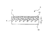
以下、本発明の好ましい実施形態について図面を参照して説明する。まず、図1を用いて、本実施形態に係る回折光学素子Dの構成について説明する。この回折光学素子Dは、1mmあたり数本から数百本の細かい溝状またはスリット状の格子構造(回折格子溝g)が同心円状に形成された回折光学面を備え、この回折光学面に入射した光を格子ピッチ(回折格子溝gの間隔)と入射光の波長とによって定まる方向へ回折する性質を有している。また、回折光学素子D(回折光学面)は、負の分散値(例えば、アッベ数=-3.453)を有し、分散が大きく、また異常分散性(例えば、部分分散比(ng-nF)/(nF-nC)=0.2956)が強いため、強力な色収差補正能力を有している。光学ガラスのアッベ数は、通常30~80程度であるが、上述のように回折光学素子のアッベ数は負の値を持っている。換言すると、回折光学素子Dの回折光学面は分散特性が通常のガラス(屈折光学素子)とは逆で光の波長が短くなるに伴い屈折率が小さくなり、長い波長の光ほど大きく曲がる性質を有している。そのため、通常の屈折光学素子と組み合わせることにより、大きな色消し効果が得られる。したがって回折光学素子Dを利用することで、通常の光学ガラスでは達し得ない良好な色収差の補正が可能になる。
また、本実施形態に係る回折光学素子Dは、異なる光学材料からなる2つの回折素子要素E1,E2を接合し、その接合面に回折格子溝gを設けて上述した回折光学面を構成している、いわゆる「密着複層型回折光学素子」である。そのため、この回折光学素子Dは、g線からC線を含む広波長域において回折効率を高くすることができる。したがって、この回折光学素子Dを用いた光学系は広波長域において利用することが可能となる。なお、回折効率は、透過型の回折光学素子Dにおいて1次回折光を利用する場合、入射強度I0と一次回折光の強度I1との割合η(=I1/I0×100[%])を示す。
ここで、密着複層型回折光学素子は、回折格子溝が形成された2つの回折素子要素をこの回折格子溝同士が対向するように近接配置してなるいわゆる分離複層型回折光学素子に比べて製造工程を簡素化することができるため、量産効率がよく、また光線の入射角に対する回折効率が良いという長所を備えている。したがって、密着複層型回折光学素子を利用した光学系は、製造が容易となり、また回折効率も良くなる。
このような密着複層型の回折光学素子Dにおいて、2つの回折素子要素E1,E2の光学材料(媒質)の屈折率の差をΔnとし、回折格子溝gの高さをdとし、この回折光学素子Dの回折光学面で回折させる光の波長をλとすると、次式(a)の条件を満足するときに、1次回折光の回折効率が100%になる。
Δn×d=λ (a)
ここで、Δλ=1-Δn×d/λとすると、上記式(a)から、このΔλが0になると回折効率が100%になる。
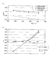
図2(a)に示す従来の低屈折率の回折素子要素と高屈折率の回折素子要素とからなる回折光学素子の場合、図2(b)に示すように、所望の波長(ここでは、d線(λ=588nm))においてΔλが0になるように設定すると、その他の波長ではこのΔλを0にすることができず、中心波長(d線)の近辺では回折効率が高いが、それよりも長い波長や短い波長においては回折効率が悪化してしまう。
そこで、本実施形態に係る回折光学素子Dでは、2つの回折素子要素E1,E2のうち、少なくともいずれか一方の光学材料(媒質)に多数の微小な空孔Bを形成し、この空孔Bが形成された回折素子要素の光学材料(媒質)の屈折率を調整している。なお、回折光学面に対向する光学面(例えば、図1において、回折素子要素E1の回折格子溝gが形成されていない方の面)の法線方向から見たときの空孔Bの径は、この回折光学面で回折させる光の波長以下であることが好ましい。この空孔B内は空気で満たされているため、この空孔Bの屈折率は1であり、また、分散は0である。そのため、回折素子要素E1を構成する光学材料に空孔Bを設けることにより、この回折素子要素E1の屈折率だけを調整することが可能となる。このとき、図2(a)に示すように、空孔Bを設けた光学材料の屈折率の波長に対する変化率は緩やかになる。そのため、透過する光の波長が短くなるほど、その光に対する屈折率が大きくなる媒質の回折素子要素E1,E2を用いて回折光学素子Dを形成した場合、波長が長くなるほど、2つの回折素子要素の媒質の屈折率の差(Δn)は大きくなる。すなわち、上述した式(a)において、回折格子溝の高さdを固定された値とすると、空孔Bを設けることにより、式(a)の条件に近づくことなる。そのため、図2(b)に示すように、空孔Bを設けた光学材料により形成された回折素子要素E1を用いると、広い波長帯域でΔλの値が0に近くなり、回折効率が向上する(図2(b)の場合では、中心波長であるd線よりも短い波長の光に対して回折効率が特に改善されることが分かる)。
このような回折光学素子Dにおいて、空孔Bが形成された回折素子要素E1の体積に対する空孔Bの体積(の総和)の割合を充填率Pとすると、この回折光学素子Dは、次式(1)の条件を満足することが望ましい。なお、充填率Pは、体積比ではなく、重量比としてもよい。
P<0.9 (1)
回折素子要素Dの空孔Bの充填率Pがこの条件式(1)の上限値を上回ると、当該回折素子要素E1の光学材料(媒質)の屈折率が低くなりすぎてしまい、もう一方の回折素子要素E2との関係で、回折光学素子Dとしての光学性能を満足することができなくなってしまう。なお、この空孔Bによる回折効率の向上に対する効果をさらに発揮させるためには、空孔Bが形成される回折素子要素E1の充填率Pが次式(1′)の条件を満足することが望ましい。
0.6<P<0.8 (1′)
なお、空孔Bを形成した光学材料からなる回折素子要素E1は、回折光学素子Dを形成する2つの回折素子要素E1,E2のうち、高屈折率・低分散の回折素子要素に形成することが好ましい。したがって、この空孔Bが形成される回折素子要素の光学材料(媒質)のd線に対する屈折率nは、次式(2)の条件を満足することが好ましい。
1.6<n<2.0 (2)
また、上述したように、1次回折光の回折効率を100%とするためには、Δλ=1-Δn×d/λを0にすることが必要である。よって、この回折光学素子Dで回折させる光の波長をF線(λ=486nm)からC線(λ=656nm)の範囲とすると、この回折光学素子Dは、F線からC線の範囲の光に対して、次式(3)の条件を満足することが望ましい。
|1-Δn×d/λ|<0.075 (3)
この条件式(3)を満足することにより、この回折光学素子Dは、F線からC線までの範囲において、高い回折効率を実現することができる。
さらに、F線からC線の範囲における中心波長をd線とすると、この回折光学素子Dは、F線からd線の範囲の光に対して、次式(3′)の条件を満足することが望ましい。
|1-Δn×d/λ|<0.030 (3′)
この条件式(3′)を満足することにより、この回折光学素子Dは、さらに高い回折効率を実現することができる。
このような空孔Bを有する光学材料で形成された回折素子要素E1は、モールドガラスでも、樹脂でもよい。また、樹脂に高屈折率物質の微粒子を混入させたものでもよい。空孔を持つ物質の作成法としては、限定するものではないが、例としてゾル-ゲル法や蒸着法、スパッタ法などがあり、ゾル-ゲル法では溶液の濃度、蒸着法では成膜時の真空度、ガス導入量などを変えて、充填率を変えることができる。材料としても、特に拘る必要はなく、酸化物、フッ化物、樹脂等が考えられる。また、回折素子要素の素材表面の必要部分にのみ防食処理を施し、腐食剤によって不要部分を溶解侵食・食刻するエッチングにより、この回折素子要素に空孔を形成してもよい。
なお、図1に示す回折光学素子Dは、平板状の2つの回折素子要素E1,E2の対向する面に回折格子溝gを形成して密着させた構成を示したが、本発明がこの構成に限定されることはない。例えば、回折格子溝gが形成される面が曲面で形成されていてもよい。また、レンズ等の光学部材のいずれかの面上に、この回折光学素子Dを形成してもよいし、2つのレンズの間にこの回折光学素子Dを配置し、全体を接合した接合レンズとしてもよい。
なお、空孔Bには空気が充填されることが好ましい。これにより、空孔Bを含む光学材料の波長に対する屈折率の変化を小さくすることができる。さらに、空孔Bへの水蒸気の浸入を防ぐことができる。
または、空孔Bには不活性ガスが充填されることが好ましい。これにより、空孔Bを含む光学材料の波長に対する屈折率の変化を小さくすることができる。さらに、空孔Bへの水蒸気の浸入を防ぐことができる。不活性ガスは、ヘリウムガス(He)、ネオンガス(Ne)、アルゴンガス(Ar)、キセノンガス(Xe)、クリプトンガス(Kr)等が使用される。
または、空孔B内は真空であることが好ましい。これにより、空孔Bを含む光学材料の波長に対する屈折率の変化をより小さくすることができる。
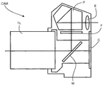
次に、上述の回折光学素子Dを備えた光学機器の一例として、回折光学素子Dを有する撮像レンズTLを備えたデジタル一眼レフカメラCAMを、図3および図4を用いて説明する。図3に示すデジタル一眼レフカメラCAMにおいて、不図示の物体(被写体)からの光は、撮像レンズTLで集光されて、クイックリターンミラーMを介して焦点板F上に結像される。焦点板F上に結像された光は、ペンタプリズムP中で複数回反射されて接眼レンズEへ導かれる。これにより、撮影者は、接眼レンズEを介して被写体の像を正立像として観察することができる。
また、撮影者によって不図示のレリーズボタンが押されると、クイックリターンミラーMが光路外へ退避し、撮像レンズTLで集光された被写体からの光は、撮像素子C上に結像されて被写体の像を形成する。これにより、被写体からの光は、撮像素子C上に結像されて当該撮像素子Cにより撮像され、被写体の画像として不図示のメモリーに記録される。このようにして、撮影者は、デジタル一眼レフカメラCAMによる被写体の撮影を行うことができる。
撮像レンズTLは、図4に示すように、光軸に沿って物体側(被写体側)から順に並んだ複数のレンズL1,L2,…を有し、第4面に上述の回折光学素子Dが形成されている。回折光学素子Dは、上述のように、広い波長帯域の光に対して回折効率を向上させることができる。そのため、撮像レンズTLは、色収差の補正等において高い光学性能を有している。したがって、デジタル一眼レフカメラCAMによれば、色収差の補正等において高い光学性能を有する光学機器を実現することができる。
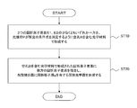
続いて、上述の回折光学素子Dの製造方法について、図5を用いて説明する。まず、2つの回折素子要素E1,E2の少なくともいずれか一方を、充填率Pが所定の条件式を満足するように空孔Bを含む光学材料(媒質)で形成する(ステップST10)。そして、空孔Bを含む光学材料で形成された回折素子要素に他方の回折素子要素を接合し、当該接合面に回折格子溝gを有する回折光学面を形成する(ステップST20)。このようにして、回折光学素子Dは製造される。
次に、実施例として、上述した回折光学素子Dを構成する2つの回折素子要素E1,E2のうち、低屈折率の回折素子要素(図1の場合は回折素子要素E2)に樹脂を用い、高屈折率の回折素子要素(図1の場合は回折素子要素E1)に、充填率80%の酸化アルミニウム(Al2O3)を用いた場合について説明する。まず、各回折素子要素の光学材料(媒質)の光の波長に対する屈折率を以下の表1に示す。なお、以下の表1には、空孔を設けていない酸化アルミニウム(すなわち、充填率が0%の場合)の屈折率も示す。
(表1)
[高屈折率の回折素子要素E1]
波長[nm] 486 588 656
酸化アルミニウム(充填率0%) 1.7700 1.7650 1.7640
酸化アルミニウム(充填率80%) 1.5792 1.5758 1.5754
[低屈折率の回折素子要素E2]
波長[nm] 486 588 656
樹脂 1.5385 1.5276 1.5754
[高屈折率の回折素子要素E1]
波長[nm] 486 588 656
酸化アルミニウム(充填率0%) 1.7700 1.7650 1.7640
酸化アルミニウム(充填率80%) 1.5792 1.5758 1.5754
[低屈折率の回折素子要素E2]
波長[nm] 486 588 656
樹脂 1.5385 1.5276 1.5754
次に、上記の回折素子要素E1,E2を用いた回折光学素子Dの回折光学面に対して垂直に入射した光(入射角=0°)の1次回折光の回折効率を表2に示す。なお、この回折光学素子Dの回折格子溝gのピッチは100μmとし、格子高さは11.7μmとする。また、回折効率の計算は、RCWA(厳密結合波:Rigorous Coupled Wave Analysis)法を用いている。
(表2)
波長[nm] 486 588 656
1次光の回折効率 98.4% 97.8% 96.6%
波長[nm] 486 588 656
1次光の回折効率 98.4% 97.8% 96.6%
この表2から明らかなように、この実施例に示す回折光学素子Dでは、F線(λ=486nm)からC線(λ=656nm)の光に対して、95%以上の回折効率を得ることができる。
また、入射角を20°とした場合の1次回折光の回折効率を表3に示す。
(表3)
波長[nm] 486 588 656
1次光の回折効率 90.4% 91.2% 91.8%
波長[nm] 486 588 656
1次光の回折効率 90.4% 91.2% 91.8%
この表3から明らかなように、この実施例に示す回折光学素子Dでは、入射角が20°であっても、F線からC線の光に対して90%以上の回折効率を得ることができる。
D 回折光学素子 E1,E2 回折素子要素 g 回折格子溝 B 空孔
Claims (18)
- 異なる光学材料からなる2つの回折素子要素を接合し、当該接合面に回折格子溝が形成された回折光学面を有する回折光学素子であって、
前記2つの回折素子要素の少なくとも一方が、空孔を含む光学材料で形成され、
前記空孔を含む光学材料が、次式の条件を満足することを特徴とする回折光学素子。
P<0.9
但し、
P:前記空孔を含む光学材料の充填率。 - 前記回折光学面に対向する光学面の法線方向から見たときの前記空孔の径が、前記回折光学面で回折させる光の波長以下であることを特徴とする請求項1に記載の回折光学素子。
- 前記空孔は、前記2つの回折素子要素のうち、屈折率が大きい回折素子要素の前記光学材料に含まれることを特徴とする請求項1に記載の回折光学素子。
- 次式の条件を満足することを特徴とする請求項1に記載の回折光学素子。
1.6<n<2.0
但し、
n:前記空孔を含む光学材料のd線に対する屈折率。 - 次式の条件を満足することを特徴とする請求項1に記載の回折光学素子。
0.6<P<0.8 - 前記回折光学面で回折させる光の波長の範囲をF線からC線までとし、当該光の中心波長をd線としたとき、F線からC線の前記光に対して次式の条件を満足することを特徴とする請求項1に記載の回折光学素子。
|1-Δn×d/λ|<0.075
但し、
Δn:前記2つの回折素子要素の前記光学材料の屈折率の差(Δn>0とする)、
d:前記回折格子溝の高さ、
λ:前記光の波長。 - 前記回折光学面で回折させる光の波長の範囲をF線からC線までとし、当該光の中心波長をd線としたとき、F線からd線の前記光に対して次式の条件を満足することを特徴とする請求項1に記載の回折光学素子。
|1-Δn×d/λ|<0.030
但し、
Δn:前記2つの回折素子要素の前記光学材料の屈折率の差(Δn>0とする)、
d:前記回折格子溝の高さ、
λ:前記光の波長。 - 前記空孔を含む光学材料は、蒸着若しくはゾル-ゲル法で製造されることを特徴とする請求項1に記載の回折光学素子。
- 前記空孔は、エッチングにより前記光学材料に形成されることを特徴とする請求項1に記載の回折光学素子。
- 前記空孔には、空気が充填されることを特徴とする請求項1に記載の回折光学素子。
- 前記空孔には、不活性ガスが充填されることを特徴とする請求項1に記載の回折光学素子。
- 前記空孔内は真空であることを特徴とする請求項1に記載の回折光学素子。
- 請求項1に記載の回折光学素子を備えることを特徴とする光学機器。
- 異なる光学材料からなる2つの回折素子要素により構成される回折光学素子の製造方法であって、
前記2つの回折素子要素の少なくとも一方を、充填率Pが次式の条件を満足するように空孔を含む光学材料で形成し、
P<0.9
前記一方の回折素子要素に他方の回折素子要素を接合し、当該接合面に回折格子溝を有する回折光学面を形成したことを特徴とする回折光学素子の製造方法。 - 前記2つの回折素子要素の少なくとも一方を、d線に対する屈折率nが次式の条件を満足する前記空孔を含む光学材料で形成したことを特徴とする請求項14に記載の回折光学素子の製造方法。
1.6<n<2.0 - 前記2つの回折素子要素の少なくとも一方を、充填率Pが次式の条件を満足するように空孔を含む光学材料で形成したことを特徴とする請求項14に記載の回折光学素子の製造方法。
0.6<P<0.8 - 前記回折光学面で回折させる光の波長の範囲をF線からC線までとし、当該光の中心波長をd線としたとき、F線からC線の前記光に対して、前記2つの回折素子要素の前記光学材料の屈折率の差Δn(Δn>0とする)、前記回折格子溝の高さd、および前記光の波長λが次式の条件を満足するようにしたことを特徴とする請求項14に記載の回折光学素子の製造方法。
|1-Δn×d/λ|<0.075 - 前記回折光学面で回折させる光の波長の範囲をF線からC線までとし、当該光の中心波長をd線としたとき、F線からd線の前記光に対して、前記2つの回折素子要素の前記光学材料の屈折率の差Δn(Δn>0とする)、前記回折格子溝の高さd、および前記光の波長λが次式の条件を満足するようにしたことを特徴とする請求項14に記載の回折光学素子の製造方法。
|1-Δn×d/λ|<0.030
Applications Claiming Priority (2)
| Application Number | Priority Date | Filing Date | Title |
|---|---|---|---|
| JP2013-111585 | 2013-05-28 | ||
| JP2013111585A JP2014232135A (ja) | 2013-05-28 | 2013-05-28 | 回折光学素子 |
Publications (1)
| Publication Number | Publication Date |
|---|---|
| WO2014192291A1 true WO2014192291A1 (ja) | 2014-12-04 |
Family
ID=51988342
Family Applications (1)
| Application Number | Title | Priority Date | Filing Date |
|---|---|---|---|
| PCT/JP2014/002792 Ceased WO2014192291A1 (ja) | 2013-05-28 | 2014-05-27 | 回折光学素子、光学機器、および回折光学素子の製造方法 |
Country Status (2)
| Country | Link |
|---|---|
| JP (1) | JP2014232135A (ja) |
| WO (1) | WO2014192291A1 (ja) |
Cited By (1)
| Publication number | Priority date | Publication date | Assignee | Title |
|---|---|---|---|---|
| CN111708112A (zh) * | 2020-08-20 | 2020-09-25 | 歌尔股份有限公司 | 液晶体光栅的制作方法 |
Families Citing this family (1)
| Publication number | Priority date | Publication date | Assignee | Title |
|---|---|---|---|---|
| JP2026060527A (ja) * | 2024-09-27 | 2026-04-08 | 日東電工株式会社 | 光学積層体 |
Citations (2)
| Publication number | Priority date | Publication date | Assignee | Title |
|---|---|---|---|---|
| JP2001044190A (ja) * | 1999-08-04 | 2001-02-16 | Hitachi Chem Co Ltd | 樹脂組成物、樹脂膜の形成方法及び半導体装置 |
| JP2011221510A (ja) * | 2010-03-26 | 2011-11-04 | Panasonic Corp | 回折光学素子及び光学機器 |
-
2013
- 2013-05-28 JP JP2013111585A patent/JP2014232135A/ja active Pending
-
2014
- 2014-05-27 WO PCT/JP2014/002792 patent/WO2014192291A1/ja not_active Ceased
Patent Citations (2)
| Publication number | Priority date | Publication date | Assignee | Title |
|---|---|---|---|---|
| JP2001044190A (ja) * | 1999-08-04 | 2001-02-16 | Hitachi Chem Co Ltd | 樹脂組成物、樹脂膜の形成方法及び半導体装置 |
| JP2011221510A (ja) * | 2010-03-26 | 2011-11-04 | Panasonic Corp | 回折光学素子及び光学機器 |
Cited By (2)
| Publication number | Priority date | Publication date | Assignee | Title |
|---|---|---|---|---|
| CN111708112A (zh) * | 2020-08-20 | 2020-09-25 | 歌尔股份有限公司 | 液晶体光栅的制作方法 |
| CN111708112B (zh) * | 2020-08-20 | 2021-01-22 | 歌尔股份有限公司 | 液晶体光栅的制作方法 |
Also Published As
| Publication number | Publication date |
|---|---|
| JP2014232135A (ja) | 2014-12-11 |
Similar Documents
| Publication | Publication Date | Title |
|---|---|---|
| JP4630645B2 (ja) | 光学系 | |
| JP5264223B2 (ja) | 回折光学素子、光学系及び光学機器 | |
| US9030755B2 (en) | Zoom lens system, optical apparatus, and method for manufacturing zoom lens system | |
| US9625689B2 (en) | Optical system, optical apparatus equipped therewith, and method for manufacturing optical system | |
| US8941921B2 (en) | Optical system, optical apparatus, and method for manufacturing optical system | |
| US8830592B2 (en) | Zoom lens, imaging apparatus, and method for manufacturing zoom lens | |
| JP2013156405A (ja) | 撮影光学系及びそれを有する撮像装置 | |
| JP2012018380A (ja) | 回折光学素子、光学系、及び、光学機器 | |
| JP5311200B2 (ja) | 広角レンズ、光学装置 | |
| WO2014025015A1 (ja) | 変倍光学系、光学装置、変倍光学系の製造方法 | |
| JP2009192996A (ja) | レンズ系及びこれを有する光学装置 | |
| JP2019074551A (ja) | 回折光学素子、光学系、および、撮像装置 | |
| CN103477266B (zh) | 变焦光学系统及具有其的拍摄装置 | |
| JP5621562B2 (ja) | 撮影レンズ、この撮影レンズを備える光学機器 | |
| JP5333406B2 (ja) | 撮影レンズ、光学機器、撮影レンズの製造方法 | |
| JP5724385B2 (ja) | 変倍光学系、この変倍光学系を備える光学機器、及び、変倍光学系の製造方法 | |
| JP5440810B2 (ja) | 光学系、光学装置 | |
| JP5464379B2 (ja) | 光学系、光学装置 | |
| JP5464380B2 (ja) | 光学系、光学装置 | |
| JP2014232135A (ja) | 回折光学素子 | |
| JP4743607B2 (ja) | フレネルレンズ、および、このフレネルレンズを用いた液晶プロジェクタ | |
| JP5978848B2 (ja) | 変倍光学系、光学装置 | |
| JP2004126397A (ja) | 望遠レンズ | |
| JP4898205B2 (ja) | 光学系及びそれを有する光学機器 | |
| JP2015084038A (ja) | 変倍光学系、光学装置、変倍光学系の製造方法 |
Legal Events
| Date | Code | Title | Description |
|---|---|---|---|
| 121 | Ep: the epo has been informed by wipo that ep was designated in this application |
Ref document number: 14804305 Country of ref document: EP Kind code of ref document: A1 |
|
| NENP | Non-entry into the national phase |
Ref country code: DE |
|
| 122 | Ep: pct application non-entry in european phase |
Ref document number: 14804305 Country of ref document: EP Kind code of ref document: A1 |