WO2014192274A1 - 有機光電変換素子および撮像素子 - Google Patents
有機光電変換素子および撮像素子 Download PDFInfo
- Publication number
- WO2014192274A1 WO2014192274A1 PCT/JP2014/002746 JP2014002746W WO2014192274A1 WO 2014192274 A1 WO2014192274 A1 WO 2014192274A1 JP 2014002746 W JP2014002746 W JP 2014002746W WO 2014192274 A1 WO2014192274 A1 WO 2014192274A1
- Authority
- WO
- WIPO (PCT)
- Prior art keywords
- film
- photoelectric conversion
- organic
- layer
- protective film
- Prior art date
- Legal status (The legal status is an assumption and is not a legal conclusion. Google has not performed a legal analysis and makes no representation as to the accuracy of the status listed.)
- Ceased
Links
Images
Classifications
-
- H—ELECTRICITY
- H10—SEMICONDUCTOR DEVICES; ELECTRIC SOLID-STATE DEVICES NOT OTHERWISE PROVIDED FOR
- H10K—ORGANIC ELECTRIC SOLID-STATE DEVICES
- H10K39/00—Integrated devices, or assemblies of multiple devices, comprising at least one organic radiation-sensitive element covered by group H10K30/00
- H10K39/30—Devices controlled by radiation
- H10K39/32—Organic image sensors
-
- H—ELECTRICITY
- H10—SEMICONDUCTOR DEVICES; ELECTRIC SOLID-STATE DEVICES NOT OTHERWISE PROVIDED FOR
- H10K—ORGANIC ELECTRIC SOLID-STATE DEVICES
- H10K30/00—Organic devices sensitive to infrared radiation, light, electromagnetic radiation of shorter wavelength or corpuscular radiation
- H10K30/80—Constructional details
- H10K30/88—Passivation; Containers; Encapsulations
-
- Y—GENERAL TAGGING OF NEW TECHNOLOGICAL DEVELOPMENTS; GENERAL TAGGING OF CROSS-SECTIONAL TECHNOLOGIES SPANNING OVER SEVERAL SECTIONS OF THE IPC; TECHNICAL SUBJECTS COVERED BY FORMER USPC CROSS-REFERENCE ART COLLECTIONS [XRACs] AND DIGESTS
- Y02—TECHNOLOGIES OR APPLICATIONS FOR MITIGATION OR ADAPTATION AGAINST CLIMATE CHANGE
- Y02E—REDUCTION OF GREENHOUSE GAS [GHG] EMISSIONS, RELATED TO ENERGY GENERATION, TRANSMISSION OR DISTRIBUTION
- Y02E10/00—Energy generation through renewable energy sources
- Y02E10/50—Photovoltaic [PV] energy
- Y02E10/549—Organic PV cells
-
- Y—GENERAL TAGGING OF NEW TECHNOLOGICAL DEVELOPMENTS; GENERAL TAGGING OF CROSS-SECTIONAL TECHNOLOGIES SPANNING OVER SEVERAL SECTIONS OF THE IPC; TECHNICAL SUBJECTS COVERED BY FORMER USPC CROSS-REFERENCE ART COLLECTIONS [XRACs] AND DIGESTS
- Y02—TECHNOLOGIES OR APPLICATIONS FOR MITIGATION OR ADAPTATION AGAINST CLIMATE CHANGE
- Y02P—CLIMATE CHANGE MITIGATION TECHNOLOGIES IN THE PRODUCTION OR PROCESSING OF GOODS
- Y02P70/00—Climate change mitigation technologies in the production process for final industrial or consumer products
- Y02P70/50—Manufacturing or production processes characterised by the final manufactured product
Definitions
- the present invention relates to an organic photoelectric conversion element formed by laminating a photoelectric conversion layer made of an organic material on a plurality of pixel electrodes, which is used for an imaging device, a display device, and the like. Further, the present invention relates to an imaging device provided with an organic photoelectric conversion device.
- Image sensors such as CCD sensors and CMOS sensors are widely known as image sensors used in digital still cameras, digital video cameras, cameras for mobile phones, cameras for endoscopes, and the like.
- imaging devices having a photoelectric conversion layer made of an organic material have been studied.
- An imaging device having an organic photoelectric conversion layer includes a pixel electrode formed on a semiconductor substrate on which a signal readout circuit is formed, an organic photoelectric conversion layer formed on the pixel electrode, and an organic photoelectric conversion layer A transparent counter electrode (upper electrode), a protective film formed on the counter electrode to protect the counter electrode, and a color filter or the like.
- a protective film is formed on the organic photoelectric conversion layer by low temperature plasma CVD at about room temperature to 80 ° C. in order to prevent deterioration of the organic layer due to penetration of oxygen or water. It is known to do (patent document 2).
- Patent Document 2 discloses a photoelectric conversion film-stacked solid-state imaging device using an organic semiconductor, in which a protective layer made of an inorganic material is formed above the transparent counter electrode.
- the inorganic material constituting the protective layer is made of silicon oxide, silicon nitride, or silicon nitride oxide, and is formed by plasma CVD capable of forming a film at a low temperature (ordinary temperature).
- Patent Document 3 proposes an imaging device in which the film stress is suppressed to ⁇ 200 MPa to 250 MPa by forming the protective film from a plurality of layers of different film stresses.
- Patent Document 4 proposes an imaging device in which a layer having an internal stress of 100 MPa or less is provided between the counter electrode and the sealing film (protective film) as a sealing auxiliary layer.
- Patent Document 5 As an element having an organic layer and an electrode, not only an imaging element but also an organic EL element in which an organic light emitting material is disposed between a pair of electrodes facing each other on a substrate is known (see Patent Document 5).
- the organic EL element described in Patent Document 5 has a protective layer corresponding to a sealing film on the surface of the organic light emitting material, and the protective layer is formed by laminating layers different in stress generated inside. Relieves the internal stress of the protective layer.
- JP, 2011-71469 A Unexamined-Japanese-Patent No. 2006-245045 JP 2011-228648 A JP 2012-124343 A Japanese Patent Application Publication No. 2001-284042
- the stress of the entire protective film is reduced by forming the protective film with a laminated film of silicon oxynitride (SiON) having compressive stress and aluminum oxide (AlO) having tensile stress.
- SiON silicon oxynitride
- AlO aluminum oxide
- Silicon oxynitride can form a thick film in a relatively short time, but aluminum oxide takes time to form a thick film, and forming both layers with the same thickness is inferior in mass productivity. There is.
- soldering a component such as a photoelectric conversion element
- solder paste is printed on a printed circuit board, parts are placed on it, and the solder is melted and heated by heating from 220 ° C to 260 ° C for about 10 seconds. I do.
- an organic photoelectric conversion element having a configuration that can withstand the reflow including the high temperature heating step is required.
- the present invention has been made in view of the above circumstances, and it is an object of the present invention to provide an organic photoelectric conversion element and an imaging element provided with the organic photoelectric conversion element, which have high mass productivity and can reduce manufacturing costs. I assume.
- the organic photoelectric conversion device of the present invention is A substrate, A plurality of pixel electrodes spaced apart from each other on the substrate; An organic film including a photoelectric conversion layer disposed in a continuous film shape on a plurality of pixel electrodes and between the pixel electrodes; A counter electrode disposed on the organic film, And a protective film disposed on the counter electrode,
- the step between the upper surface of the pixel electrode and the surface of the substrate is 3 nm or more and 100 nm or less,
- the inclination angle of the end of the pixel electrode is 10 ° or more and 90 ° or less
- the internal stress of the protective film is -600 MPa or more and less than -200 MPa,
- the product of the film thickness of the protective film and the internal stress is ⁇ 40,000 MPa ⁇ nm or more and less than ⁇ 14,000 MPa ⁇ nm.
- the protective film is preferably composed of an aluminum oxide layer and a silicon oxynitride layer.
- the thickness of the aluminum oxide layer is preferably 1 ⁇ 5 or less of the total thickness of the protective film. At this time, the thickness of the aluminum oxide layer is more preferably 10 nm or less.
- the protective film may be composed of only a silicon oxynitride layer. At this time, a plurality of layers having different oxygen and nitrogen ratios in the silicon oxynitride layer (SiOxNy) may be included.
- the internal stress of the protective film is more preferably -400 MPa or more and less than -200 MPa.
- the inclination angle of the end of the pixel electrode is more preferably 30 ° or more and 90 ° or less.
- the level difference between the pixel electrode and the substrate surface is more preferably 5 nm or more and 40 nm or less.
- the imaging device of the present invention is characterized by having the organic photoelectric conversion device of the present invention.
- the step between the upper surface of the pixel electrode and the surface of the substrate is 3 nm or more and 100 nm or less, and the inclination angle of the end of the pixel electrode is 10 ° or more and 90 ° or less Since the internal stress of the film is -600 Pa or more and less than -200 MPa, even after the high temperature processing (about 10 seconds at 220 ° C. to 260 ° C.) at the time of solder reflow while sufficiently securing the protective function of the organic film by the protective film. Mechanical degradation of the organic film can be suppressed.
- the absolute value of the internal stress of the protective film is larger than that of the prior art, it is possible to select a protective film made of a material that can be easily deposited.
- a protective film mainly using silicon oxynitride film formation is easy and mass productivity is high.
- the film forming time can be set to a practical range as long as the thickness is sufficiently thin with respect to the total thickness of the protective film.
- the pixel portion in which at least the pixel electrodes are arrayed by setting the step difference from the substrate surface of the pixel electrode to 3 nm or more and 100 nm or less and the inclination angle of the end portion to 10 ° or more and 90 ° or less as in the present invention.
- the present inventors have found that the generation of wrinkles can be suppressed even at a heating temperature of about 240 ° C. for about 10 seconds.
- pewter reflow since the reflow apparatus for normal electric devices can be used, the cost of a manufacturing apparatus can be suppressed. Further, Pb-free solder which does not contain Pb, which has a large environmental load, can be used.
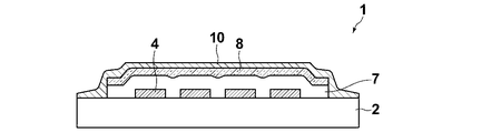
- FIG. 1 is a schematic cross-sectional view showing the configuration of the photoelectric conversion element 1 according to the embodiment of the present invention.
- the imaging device 1 of the present embodiment includes a plurality of pixel electrodes 4 arranged in a two-dimensional manner spaced apart from each other on a substrate 2, and a plurality of pixel electrodes 4 and continuous on the pixel electrodes.
- the film is formed to cover the organic film 7 including at least the photoelectric conversion layer, the counter electrode 8 disposed on the organic film 7, and the counter electrode 8 disposed in a film shape, and is formed under the film.
- a protective film 10 covering the pixel electrode 4.
- the substrate 2 is made of, for example, a silicon substrate, a glass substrate or the like.
- the pixel electrode 4 is an electrode provided independently for each pixel.
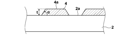
- FIG. 2 is a view for explaining the end inclination angle ⁇ of the pixel electrode and the level difference t.
- Each pixel electrode 4 has an end (a taper portion) inclined at an angle ⁇ (where 10 ° ⁇ ⁇ ⁇ 90 °) with respect to the surface 2 a of the substrate 2. If the inclination angle of the end portion of each pixel electrode 4 is in the range of 10 ° to 90 °, they may be individually different.
- the inclination angle ⁇ is more preferably 30 ° or more and 90 ° or less. When the inclination angle is larger than 90 °, the deposition beam is broken at the electrode end when depositing the organic photoelectric conversion layer, and a point defect occurs in the image.
- the difference in level t between the upper surface 4 a of each pixel electrode 4 and the surface 2 a of the substrate 2 is 3 nm ⁇ t ⁇ 100 nm.
- the level difference t is more preferably 5 nm or more and 40 nm or less.
- the step difference t exceeds 100 nm and becomes higher than the thickness of the electron blocking layer, the dark current increases.
- the step t is the thickness of the pixel electrode 4 itself.
- the step t is smaller than the thickness of the pixel electrode 4.
- Examples of the material of the pixel electrode 4 include metals, metal oxides, metal nitrides, metal borides, organic conductive compounds, and mixtures thereof.
- conductive metal oxides such as tin oxide, zinc oxide, indium oxide, indium tin oxide (ITO), indium zinc oxide (IZO), indium tungsten oxide (IWO), titanium oxide, titanium nitride (TiN)
- Metals such as gold (Au), platinum (Pt), silver (Ag), chromium (Cr), nickel (Ni), aluminum (Al), etc., and further, these metals and conductive metal oxides And laminates, organic conductive compounds such as polyaniline, polythiophene and polypyrrole, laminates of these with ITO, and the like.
- Particularly preferable materials for the pixel electrode 4 are titanium nitride, molybdenum nitride, tantalum nitride, and tungsten nitride.
- the organic film 7 includes a photoelectric conversion layer made of an organic photoelectric conversion material that generates an electric charge according to at least the received light, or an organic photoelectric conversion material that emits light by application of an electric field. It consists of Note that a layer made of an inorganic material may be included between the plurality of organic layers.
- the counter electrode 8 is an electrode that faces each pixel electrode 4 and is provided on the organic film 7.
- the counter electrode 8 is commonly provided to a plurality of pixels, and may therefore be called a common electrode (common electrode).
- the counter electrode 8 may be individually provided in correspondence with each pixel electrode.
- the counter electrode 8 has a wavelength at which the photoelectric conversion layer has sensitivity or a wavelength of emitted light, for example, visible light, in order to cause light to enter the organic film 7 including the photoelectric conversion layer or transmit emitted light. It is transparent enough.
- a transparent conductive oxide is preferably used for the counter electrode 8.
- metals, metal oxides, metal nitrides, metal borides, organic conductive compounds, mixtures thereof and the like can be mentioned. Specific examples thereof include conductive metal oxides such as tin oxide, zinc oxide, indium oxide, indium tin oxide (ITO), indium zinc oxide (IZO), indium tungsten oxide (IWO), titanium oxide, etc., metal nitrides such as TiN, etc.
- Metals such as gold (Au), platinum (Pt), silver (Ag), chromium (Cr), nickel (Ni), aluminum (Al), and mixtures or laminates of these metals and conductive metal oxides , Organic conductive compounds such as polyaniline, polythiophene and polypyrrole, laminates of these with ITO, and the like.
- Particularly preferable materials for the transparent conductive film are ITO, IZO, tin oxide, antimony-doped tin oxide (ATO), fluorine-doped tin oxide (FTO), zinc oxide, antimony-doped zinc oxide (AZO), gallium-doped zinc oxide GZO) is any material.
- the light transmittance of the counter electrode 8 is preferably 60% or more, more preferably 80% or more, more preferably 90% or more, more preferably 95% or more at the visible light wavelength.
- the counter electrode 8 preferably has a thickness of 5 to 30 nm. By setting the thickness of the counter electrode 8 to 5 nm or more, the lower layer can be sufficiently covered, and uniform performance can be obtained. On the other hand, when the film thickness of the counter electrode 8 exceeds 30 nm, the counter electrode 8 and the pixel electrode 4 may locally short-circuit, and the dark current may increase. By setting the thickness of the counter electrode 8 to 30 nm or less, the occurrence of local short circuit can be suppressed.
- the protective film 10 is for preventing the factor which degrades organic materials, such as water and oxygen, from invading the organic film 7 containing the organic material, and the organic film 7 is used over a long period of storage and long term use. Prevent the deterioration of the organic materials, such as water and oxygen, from invading the organic film 7 containing the organic material, and the organic film 7 is used over a long period of storage and long term use. Prevent the deterioration of the
- the protective film 10 may be a single layer or a plurality of layers. Here, all the insulating layers formed on the counter electrode 8 are integrally referred to as the protective film 10.
- the internal stress of the protective film 10 is -600 MPa or more and less than -200 MPa, and more preferably -400 MPa or more and less than -200 MPa.
- the protective film 10 is preferably composed of an inorganic oxide layer, and particularly preferably composed of only silicon oxynitride (SiON) or a laminate of silicon oxynitride and aluminum oxide (AlO).
- Aluminum oxide has a very high barrier property, but since it takes a considerable time to form a thick film, it is inferior in mass productivity to form a film having a thickness sufficient to exert a sufficient protective function as a protective film.
- silicon oxynitride is easy to form a thick film, but its compressive stress is very large.
- the aluminum oxide film has a tensile stress with respect to the substrate, and the silicon oxynitride film has a compressive stress.
- the film thickness of aluminum oxide is 1 ⁇ 5 or less of the total thickness of the protective film, the compressive stress of the silicon oxynitride film becomes dominant as the internal stress of the protective film.
- the internal stress due to the protective film be smaller and that the absolute value be 200 MPa or less.
- the protective film 10 has a stress of -600 MPa or more and less than -200 MPa, and more preferably -400 MPa or more and less than -200 MPa.
- the protective film 10 of the present invention has a stress greater than that of the prior art, but the internal stress of the protective film is -600 MPa by setting the inclination angle of the step and the end face from the substrate surface of the pixel electrode to the above range. As described above, the inventor has found that it is possible to suppress wrinkles even if the pressure is less than -200 MPa (see Examples described later).
- the thickness of the protective film 10 is preferably 70 to 500 nm. If the protective film 110 has a thickness of 70 nm or more, the organic film can be sufficiently protected from immersion by an acid, an alkali, or the like, and if 500 nm or less, the occurrence of color mixing can be suppressed.
- the product of the film thickness of the protective film 10 and the internal stress is made to be ⁇ 40,000 MPa ⁇ nm or more and less than ⁇ 14,000 MPa ⁇ nm. If the absolute value of the product of the film thickness and the internal stress is 40,000 or less, the effect of suppressing wrinkles due to the presence of the pixel electrode described above is effective.
- the protective film 110 is formed, for example, by a vapor deposition method.
- the vapor deposition method include plasma CVD method, atomic layer deposition CVD method, sputtering method and ion plate method.
- the protective film 110 is also transparent to incident light or emitted light.
- the internal stress is measured by the following measuring method, but the stress of the protective film is formed by the same material as the film measured by the following measuring method and under the same film forming conditions. It means that.
- a method of measuring stress from the warpage of the substrate 70 caused by the thin film 72 will be described by taking the substrate 70 on which the thin film 72 is formed as an example.
- the internal stress of the thin film 72 can be measured using an optical lever method based on the amount of warpage of the substrate 70.
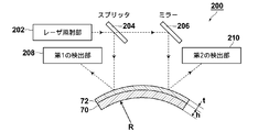
- FIG. 3 is a schematic view showing a measuring apparatus for measuring the amount of warpage of a substrate on which a thin film is formed.
- the measuring apparatus 200 illustrated in FIG. 3 includes a laser irradiation unit 202 that emits a laser beam, a splitter 204 that reflects part of the light emitted from the laser irradiation unit 202 and transmits other light, And a mirror 206 for reflecting the light transmitted through the light source 204.
- a thin film 72 which is an object to be measured is formed on one surface of the substrate 70.
- the measuring apparatus 200 by measuring the amount of warpage before and after the thin film is formed on the substrate, the amount of warpage caused by the formation of the thin film can be obtained.
- the procedure of measuring the stress of the thin film by the measuring device 200 will be described.
- a thin film stress measuring apparatus FLX-2320-S manufactured by Toago Technology, Inc. can be used as an apparatus used for the measurement.
- the measurement conditions when this device is used are shown below.
- Laser beam Laser irradiation unit 202
- Laser used KLA-Tencor-2320-S Laser power: 4mW
- Laser wavelength 670 nm
- Scanning speed 30 mm / s
- Substrate material Silicon (Si) Orientation: ⁇ 100>
- Type P type (dopant: Boron)
- Thickness 250 ⁇ 25 ⁇ m or 280 ⁇ 25 ⁇ m
- the curvature amount of the substrate 70 on which the thin film 72 is formed is measured in advance, and the curvature radius R1 of the substrate 70 is obtained. Subsequently, the thin film 72 is formed on one surface of the substrate 70, the amount of warpage of the substrate 70 on which the thin film 72 is formed is measured, and the curvature radius R2 is determined.
- the amount of warpage is scanned with the laser on the side of the substrate 70 on which the thin film 72 is formed, and the amount of warpage is calculated from the reflection angle of the laser light reflected from the substrate 70.
- the curvature radius R R1 ⁇ R2 / (R1-R2) is calculated based on the amount of warpage.
- the stress of the thin film 72 is calculated by the following formula.
- the unit of stress of the thin film 72 is represented by Pa. When it is compressive stress, it shows a negative value, and when it is tensile stress, it shows a positive value.
- the method of measuring the stress of the thin film 72 is not particularly limited, and any known method can be used.
- the method of measuring the internal stress of the thin film is as described above.
- that the internal stress of the protective film is -600 MPa or more and less than -200 MPa means that the composition and film forming conditions of the film in which the internal stress measured by the above measuring method is -600 MPa or more and less than -200 MPa Is previously determined, which means that the film is formed under the conditions.
- the stress of the protective film can be changed by adjusting the substrate temperature, pressure, input power, gas type, inter-substrate distance, and the like, for example, when forming a film by CVD or sputtering.
- the photoelectric conversion element as described above When the photoelectric conversion element as described above is provided with a photoelectric conversion layer that receives light and generates electric charge, when light is incident from above the counter electrode 8 with the counter electrode 8 as an electrode on the light incident side, Light passes through the counter electrode 8 and is incident on the photoelectric conversion layer of the organic film 7 to generate charges in the photoelectric conversion layer. The holes among the generated charges move to the pixel electrode 4. By converting the holes moved to the pixel electrode 4 into a voltage signal corresponding to the amount and reading the light, light can be converted into a voltage signal and extracted.
- the photoelectric conversion element includes a photoelectric conversion layer that converts an electrical signal into light, a light emitting element that converts a voltage signal (electric field) applied between the pixel electrode 4 and the counter electrode 8 into light. Can be used as a so-called EL element.
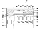
- FIG. 4 is a schematic cross-sectional view showing an imaging device according to an embodiment of the present invention.
- the imaging device according to the embodiment of the present invention can be used in an imaging device such as a digital camera or a digital video camera. Furthermore, it is mounted and used for imaging modules, such as an electronic endoscope and a mobile telephone.
- the solid-state imaging device 100 shown in FIG. 4 includes a substrate 101, an insulating layer 102, a connection electrode 103, a pixel electrode 104, a connection portion 105, a connection portion 106, an organic film 107, a counter electrode 108, and protection.
- the film 110, the color filter 111, the partition wall 112, the light shielding layer 113, the surface protection layer 114, the counter electrode voltage supply unit 115, and the readout circuit 116 are provided.
- the pixel electrode 104, the organic film 107, the counter electrode 108 and the protective film 110 in the solid-state imaging device 100 correspond to the pixel electrode 4, the organic film 7, the counter electrode 8 and the protective film 10 of the photoelectric conversion element 1 described above. It is a thing.
- the substrate 101 is a glass substrate or a semiconductor substrate such as Si.
- An insulating layer 102 is formed on the substrate 101.
- a plurality of pixel electrodes 104 two-dimensionally arranged in a state where the surface is viewed vertically are formed.
- the connection electrode 103 is formed on the insulating layer 102.
- the connection electrode 103 and the plurality of pixel electrodes 104 are respectively located on the surface of the insulating layer 102, and the lower surface of the connection electrode 103 and the lower surface of each pixel electrode 104 are substantially flush with the surface of the insulating layer 102.
- the pixel electrode 104 is a charge collection electrode for collecting a charge generated in an organic photoelectric conversion layer (hereinafter, also simply referred to as a photoelectric conversion layer) of the organic film 107 described later.
- a readout circuit 116 connected to each of the plurality of pixel electrodes 104 and a counter electrode voltage supply unit 115 connected to the connection electrode 103 are formed.
- the organic film 107 is formed on the insulating layer 102 and each pixel electrode 104.
- the organic film 107 includes a photoelectric conversion layer.
- the photoelectric conversion layer is a layer that generates charge by photoelectrically converting incident light.
- the organic film 107 is provided on the plurality of pixel electrodes 104 so as to cover them.
- the organic film 107 has a constant film thickness on the pixel electrode 104, but the film thickness may be changed outside the pixel portion (outside the effective pixel region). Details of the organic film 107 will be described later. Note that the organic film 107 may include not only a layer made of only an organic material but also a layer of an inorganic material.
- the counter electrode 108 is an electrode facing the pixel electrode 104, and is provided on the organic film 107 so as to cover the organic film 107.
- the counter electrode 108 is made of a conductive material that is transparent to incident light in order to cause light to be incident on the organic film 107.
- the counter electrode 108 is provided on the organic film 107, and is formed on the insulating layer 102 so as to extend on the connection electrode 103 disposed outside the outer peripheral edge of the organic film 107. Connected.
- connection portions 105 and 106 are embedded in the insulating layer 102.
- the connection portion 105 electrically connects the pixel electrode 104 and the readout circuit 116.
- the connection unit 106 electrically connects the connection electrode 103 and the counter electrode voltage supply unit 115.
- the connection portions 105 and 106 are columnar members made of a conductive material, and are, for example, via plugs.
- the counter electrode voltage supply unit 115 is formed on the substrate 101, and applies a predetermined voltage to the counter electrode 108 through the connection portion 106 and the connection electrode 103.
- the power supply voltage is boosted by a charge pump or other not shown booster circuit to supply the predetermined voltage.
- the readout circuit 116 is provided on the substrate 101 to correspond to each of the plurality of pixel electrodes 104.
- the readout circuit 116 reads out a signal corresponding to the charge collected by the pixel electrode 104.
- the readout circuit 116 is configured by a CMOS circuit.
- the readout circuit 116 is shielded from light by a light shielding layer (not shown) provided on the insulating layer 102.
- a CCD or CMOS circuit it is preferable to employ a CCD or CMOS circuit. From the viewpoint of high speed, it is preferable to use a CMOS circuit.
- the readout circuit 116 may be configured of a CCD circuit, a TFT circuit, or the like.
- a protective film 110 is formed on the counter electrode 108.
- the protective film 110 blocks oxygen and water from entering the organic film 107 by shielding oxygen and water.
- the protective film 110 may be composed of a plurality of layers. Further, the internal stress of the entire protective film 110 is within a predetermined range.
- a plurality of color filters 111 two-dimensionally arranged are formed on the protective film 110.
- the plurality of color filters 111 are formed above the respective pixel electrodes 104.
- the partition wall 112 is formed in a lattice shape, isolates adjacent color filters 111, and can suppress incident light from entering the color filters of other pixel portions, and the light transmission efficiency of each pixel portion Improve.
- the light shielding layer 113 is formed on the protective film 110 except the area where the color filter 111 and the partition wall 112 are provided. Thus, the light shielding layer 113 prevents light from entering the region covering the region other than the region where the plurality of pixel electrodes 104 are arranged in the organic film 107.
- the surface protective layer 114 is formed to cover the color filter 111, the partition wall 112, and the light shielding layer 113, and protects the surface on the light incident side in the imaging device.
- connection electrodes 103, a plurality of connection portions 106, and a plurality of counter electrode voltage supply portions 115 may be provided, or one each.
- the counter electrode 108 is provided as a control with respect to the center of the counter electrode 108, and a voltage is supplied to the counter electrode 108 from each counter electrode voltage supply unit 115. Voltage drop can be suppressed.
- a region including at least one pixel electrode 104, the organic film 107, and the counter electrode 108 facing the pixel electrode 104 can be defined as one pixel portion.
- the imaging device 100 is configured by arranging a plurality of pixel units in an array.
- the organic film 107 may include a charge blocking layer in addition to the photoelectric conversion layer.
- the charge blocking layer has a function of suppressing dark current.
- the charge blocking layer may be composed of a plurality of layers, for example, may be composed of a first blocking layer and a second blocking layer. As described above, by forming the charge blocking layer into a plurality of layers, an interface is formed between the first blocking layer and the second blocking layer, and a discontinuity occurs in the intermediate level present in each layer, whereby the intermediate layer is formed. It becomes difficult for charge carriers to move through the levels, and dark current can be suppressed. Note that the charge blocking layer may be a single layer.
- the photoelectric conversion layer includes a p-type organic semiconductor and an n-type organic semiconductor.
- the exciton dissociation efficiency can be increased by bonding a p-type organic semiconductor and an n-type organic semiconductor to form a donor-acceptor interface. For this reason, the photoelectric conversion layer of the structure which joined the p-type organic semiconductor and the n-type organic semiconductor expresses high photoelectric conversion efficiency.
- a photoelectric conversion layer in which a p-type organic semiconductor and an n-type organic semiconductor are mixed is preferable because the junction interface is increased and the photoelectric conversion efficiency is improved.
- the p-type organic semiconductor is a donor-type organic semiconductor, mainly represented by a hole-transporting organic compound, and refers to an organic compound having a property of easily giving an electron. More specifically, it refers to an organic compound having a smaller ionization potential when used in contact with two organic materials. Therefore, as the dona organic compound, any organic compound having an electron donating property can be used.
- the metal complex etc. which it has as can be used.
- the present invention is not limited to this, and as described above, any organic compound having a smaller ionization potential than the organic compound used as the n-type (acceptor property) compound may be used as the donor
- An n-type organic semiconductor is an acceptor-type organic semiconductor, mainly represented by an electron transporting organic compound, and refers to an organic compound having a property of easily accepting an electron. More specifically, an n-type organic semiconductor refers to an organic compound having a larger electron affinity when used in contact with two organic compounds. Therefore, as the acceptor type organic compound, any organic compound can be used as long as it is an electron accepting organic compound.
- fused aromatic carbocyclic compounds naphthalene derivative, anthracene derivative, phenanthrene derivative, tetracene derivative, pyrene derivative, perylene derivative, fluoranthene derivative
- 5- to 7-membered heterocyclic compound containing nitrogen atom, oxygen atom, sulfur atom Eg pyridine, pyrazine, pyrimidine, pyridazine, triazine, quinoline, quinoxaline, quinazoline, quintaline, phthalazine, cinnoline, isoquinoline, pteridine, acridine, phenazine, phenanthroline, tetrazole, pyrazole, imidazole, thiazole, oxazole, indazole, benzimidazole, benzotriazole, Benzoxazole, benzothiazole, carbazole, purine, triazolopyridazine, triazolopyrim
- Any organic dye may be used as the p-type organic semiconductor or n-type organic semiconductor, but preferably, cyanine dyes, styryl dyes, hemicyanine dyes, merocyanine dyes (including zero methine merocyanine (simple merocyanine)), 3 Nuclear merocyanine dyes, tetranuclear merocyanine dyes, rhodacyanine dyes, complex cyanine dyes, complex merocyanine dyes, allopolar dyes, oxonol dyes, hemioxonol dyes, squalium dyes, croconium dyes, azomethine dyes, coumarin dyes, arylidene dyes, anthraquinone dyes, tri Phenylmethane dyes, azo dyes, azomethine dyes, spiro compounds, metallocene dyes, fluorenone dyes, fulgide dyes, pery
- fullerene or a fullerene derivative excellent in electron transportability As the n-type organic semiconductor, it is particularly preferable to use a fullerene or a fullerene derivative excellent in electron transportability.
- fullerenes fullerenes, fullerene C 60 , fullerene C 70 , fullerene C 76 , fullerene C 78 , fullerene C 80 , fullerene C 82 , fullerene C 84 , fullerene C 90 , fullerene C 96 , fullerene C 240 , fullerene C 240 , fullerene C 540 , mixed A fullerene, a fullerene nanotube is represented, and a fullerene derivative represents the compound to which the substituent was added to these.
- the substituent of the fullerene derivative is preferably an alkyl group, an aryl group or a heterocyclic group.
- the alkyl group is more preferably an alkyl group having 1 to 12 carbon atoms, and the aryl group and the heterocyclic group are preferably a benzene ring, naphthalene ring, anthracene ring, phenanthrene ring, fluorene ring, triphenylene ring, naphthacene ring , Biphenyl ring, pyrrole ring, furan ring, thiophene ring, imidazole ring, oxazole ring, thiazole ring, pyridine ring, pyrazine ring, pyrimidine ring, pyridazine ring, indolizine ring, indole ring, benzofuran ring, benzothiophene ring, isobenzofuran Ring, benzimidazo
- substituents may further have a substituent, and the substituent may combine to form a ring as much as possible.
- the substituent may have a plurality of substituents, and they may be the same or different. Also, a plurality of substituents may be combined as much as possible to form a ring.
- the photoelectric conversion layer contains a fullerene or a fullerene derivative
- electrons generated by photoelectric conversion can be rapidly transported to the pixel electrode 104 or the counter electrode 108 through the fullerene molecule or the fullerene derivative molecule.
- a fullerene molecule or a fullerene derivative molecule is linked to form an electron path, electron transportability is improved, and high speed responsiveness of the photoelectric conversion element can be realized.
- it is preferable that 40% or more of the fullerene or the fullerene derivative is contained in the photoelectric conversion layer.
- the amount of the fullerene or the fullerene derivative is too large, the amount of the p-type organic semiconductor decreases, the junction interface becomes small, and the exciton dissociation efficiency decreases.
- the fullerene or fullerene derivative contained in the photoelectric conversion layer preferably has a composition of 85% or less.
- An electron donating organic material can be used for the first blocking layer and the second blocking layer.
- low molecular weight materials such as N, N'-bis (3-methylphenyl)-(1,1'-biphenyl) -4,4'-diamine (TPD) and 4,4'-bis [N Aromatic diamine compounds such as-(naphthyl) -N-phenyl-amino] biphenyl ( ⁇ -NPD), oxazole, oxadiazole, triazole, imidazole, imidazolone, stilbene derivative, pyrazoline derivative, tetrahydroimidazole, polyarylalkane, butadiene 4,4 ', 4 "-tris (N- (3-methylphenyl) N-phenylamino) triphenylamine (m-MTDATA), porphine, tetraphenylporphine copper, phthalocyanine, copper phthalocyanine, titanium phthalocyanine oxide, etc.
- Porphyrin compound, triazole derivative, oxa Use of zazole derivatives, imidazole derivatives, polyarylalkane derivatives, pyrazoline derivatives, pyrazolone derivatives, phenylenediamine derivatives, arylamine derivatives, amino-substituted chalcone derivatives, oxazole derivatives, styrylanthracene derivatives, fluorenone derivatives, hydrazone derivatives, silazane derivatives, etc.
- polymers such as phenylene vinylene, fluorene, carbazole, indole, pyrene, pyrrole, picoline, thiophene, acetylene, diacetylene and derivatives thereof can be used, even if it is not an electron donating compound, It is possible to use a compound having sufficient hole transportability.
- An inorganic material can also be used as the charge blocking layer.
- the inorganic material has a dielectric constant larger than that of the organic material, when it is used for the charge blocking layer, a large voltage is applied to the photoelectric conversion layer, and the photoelectric conversion efficiency can be increased.
- Materials that can be a charge blocking layer include calcium oxide, chromium oxide, chromium oxide copper, manganese oxide, cobalt oxide, nickel oxide, copper oxide, gallium oxide, gallium oxide, strontium oxide, niobium oxide, molybdenum oxide, indium oxide copper, oxide There are indium silver, iridium oxide and the like.
- the layer adjacent to the photoelectric conversion layer among the plurality of layers is a layer made of the same material as the p-type organic semiconductor contained in the photoelectric conversion layer.
- the same p-type organic semiconductor as the charge blocking layer, formation of an intermediate level at the interface between the photoelectric conversion layer and the layer adjacent thereto can be suppressed, and dark current can be further suppressed.
- the charge blocking layer is a single layer, it can be a layer consisting of an inorganic material, or, in the case of multiple layers, one or more layers can be a layer consisting of an inorganic material .
- the pixel electrode 104 collects charges of electrons or holes generated in the organic film 107 including the photoelectric conversion layer on the pixel electrode 104.
- the charge collected by each pixel electrode 104 becomes a signal in the readout circuit 116 of each corresponding pixel, and an image is synthesized from the signals acquired from a plurality of pixels.
- the details of the pixel electrode 104 are the same as those described for the photoelectric conversion element 1, and the thickness from the surface of the substrate (here, the surface of the insulating layer 102) is 3 nm or more and 100 nm or less, preferably 5 nm or more and 40 nm
- the angle ⁇ of the end portion is 10 ° or more and 90 ° or less, preferably 30 ° or more and 90 ° or less.
- the counter electrode 108 applies an electric field to the organic film 107 by sandwiching the organic film 107 including the photoelectric conversion layer together with the pixel electrode 104, and collects the charges generated in the photoelectric conversion layer with the pixel electrode 104. It collects charge with the opposite polarity to the signal charge.
- the counter electrode 108 can be shared by a plurality of pixels because it is not necessary to divide the collection of the reverse polarity charge among the pixels. Therefore, it may be called a common electrode (common electrode).
- the counter electrode 108 is preferably made of a transparent conductive film in order to allow light to be incident on the organic film 107 including the photoelectric conversion layer, and for example, metal, metal oxide, metal nitride, metal boride, organic conductive property Compounds, mixtures thereof and the like can be mentioned. Specific examples thereof include conductive metal oxides such as tin oxide, zinc oxide, indium oxide, indium tin oxide (ITO), indium zinc oxide (IZO), indium tungsten oxide (IWO), titanium oxide, etc., metal nitrides such as TiN, etc.
- Metals such as gold (Au), platinum (Pt), silver (Ag), chromium (Cr), nickel (Ni), aluminum (Al), and mixtures or laminates of these metals and conductive metal oxides , Organic conductive compounds such as polyaniline, polythiophene and polypyrrole, laminates of these with ITO, and the like.
- Particularly preferable materials for the transparent conductive film are ITO, IZO, tin oxide, antimony-doped tin oxide (ATO), fluorine-doped tin oxide (FTO), zinc oxide, antimony-doped zinc oxide (AZO), gallium-doped zinc oxide GZO) is any material.
- the surface resistance of the counter electrode 108 is preferably 10 k ⁇ / ⁇ or less, more preferably 1 k ⁇ / ⁇ or less, when the readout circuit 116 is a CMOS type.
- the readout circuit 116 is a CCD type, 1 k ⁇ / ⁇ or less is preferable, and more preferably 0.1 k ⁇ / ⁇ or less.
- a color filter 111 is provided in each of the plurality of pixel portions.
- the partition wall 112 provided between the color filters 111 adjacent to each other among the plurality of pixel portions functions as a condensing unit for condensing light incident on the pixel portion on the photoelectric conversion layer of the pixel portion.
- any of the first to third color filters may be formed outside the effective pixel area, the process of forming only the light shielding layer 113 can be omitted, and the manufacturing cost can be suppressed.
- the partition formation process can be performed either after the light shielding layer formation process, after the first color color filter formation process, after the second color color filter formation process, or after the third color color filter formation process, and the manufacturing technology to be used, manufacture It can be selected as appropriate depending on the combination of methods.
- the protective film 110 is the same as that described for the protective film 10 of the photoelectric conversion element, and the internal stress is -600 MPa or more and less than -200 MPa, preferably -400 MPa or more and less than -200 MPa. And the product of which is ⁇ 40,000 MPa ⁇ nm or more and ⁇ 14,000 MPa ⁇ nm or less. Details are as described in the section of the photoelectric conversion element.
- the imaging devices of the example and the comparative example were manufactured by the following procedure.
- the imaging device of each example has the same configuration except that the configuration of the protective film, the height of the end of the pixel electrode, and the angle are different from each other.
- the readout circuit 116, the wiring layer including the connection portion 105, the insulating layer 102, and the pixel electrode 104 were manufactured on the substrate 101 by a standard CMOS image sensor process.
- the pixel electrode size was 3 ⁇ m (3 ⁇ m ⁇ 3 ⁇ m square).
- the taper angle of the pixel of each example and comparative example and the height of the step (the thickness of the pixel electrode) will be described later.
- the pressure in the chamber was reduced to 1 ⁇ 10 ⁇ 4 Pa or less.
- An electron blocking layer was deposited on the pixel electrode to a thickness of 100 nm at a deposition rate of 10 to 12 nm / s by a resistance heating deposition method while rotating the holder for holding the substrate.
- the material represented by the chemical formula 1 (fullerene C 60 ) and the material represented by the chemical formula 2 are used at deposition rates of 16 to 18 nm / s and 25 to 28 nm / s, respectively, and the volume ratio of chemical formula 1 to chemical formula 2 is 1: 3. It co-evaporated so that it might become and the photoelectric converting layer was formed.
- the thickness was 400 nm. After that, it was transported to a sputtering chamber, and an ITO film as a counter electrode was formed to a thickness of 10 nm on the photoelectric conversion layer by RF magnetron sputtering.
- the configuration and film thickness of the sealing film of each of the example and the comparative example are shown in Table 1.
- the AlOx film was formed using trimethylaluminum and water by an atomic deposition method.
- AlOx was deposited under the condition of an internal stress of 450 MPa.
- the silicon oxynitride film (hereinafter sometimes referred to as a SiON film) was formed by introducing SiH 4 , NH 3 , N 2 O, N 2 as a reaction gas using a plasma CVD method. .
- the film forming temperature was 180 ° C.
- the film forming pressure was 110 Pa
- the internal stress was adjusted by changing the film forming power from 100 to 475 W.
- the protective films of Examples 1 to 10 and Comparative Examples 1 to 5 are respectively formed of a laminated film of an AlOx film and a silicon oxynitride film in Examples 11 and 12 and Comparative Example 6 only.
- the imaging element was manufactured in the above procedure.
- the film stress is measured by thin film stress measurement using FLA-2320 manufactured by KLA-Tencor, that is, the method of measuring the change of the curvature radius of the substrate before and after thin film deposition by a laser scan under room temperature in the air. It measured by.
- films are formed on a silicon substrate, and films are formed under the same film forming conditions as the thin film having a stress measured by the film stress measurement method.
- Table 1 summarizes the configuration conditions of each Example and Comparative Example, and the evaluation results.
- Example 1 has the same stress as Comparative Example 2, the steps of the pixel electrode and the taper angles are within the scope of the present invention. From these examples, it is clear that the generation of wrinkles can be suppressed if the step of the pixel electrode satisfies the conditions of 3 nm or more and the taper angle of 10 ° or more even if the stress is less than -200 MPa.
- Comparative Example 4 was not suitable for practical use because the step of the pixel electrode exceeded 100 nm and the dark current became large.
- the stress ⁇ film thickness of the protective film was smaller than ⁇ 40,000 MPa ⁇ nm (large as an absolute value), and wrinkles after heating occurred.
- Examples 11 and 12 when the protective film is formed of a plurality of layers, a satisfactory protective film can be obtained if the range of the present invention is satisfied.
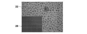
- FIG. 5 shows an area after the pixel electrode has a step, and after forming an organic layer consisting of an electron block layer and a photoelectric conversion layer, a transparent electrode and a protective film (internal stress-350 MPa) on a flat substrate area without a pixel electrode.
- the area 22 where the pixel electrode is formed and the area where the white wavy wrinkles are otherwise generated is an area where the pixel electrode is not formed, that is, a flat substrate.
- the stress of the protective film is large, it is clear that the effect obtained by providing an electrode having a level difference with the substrate surface is remarkable.
Landscapes
- Physics & Mathematics (AREA)
- Electromagnetism (AREA)
- Solid State Image Pick-Up Elements (AREA)
- Light Receiving Elements (AREA)
Abstract
【課題】量産性が高く、半田リフローによる劣化を生じない有機光電変換素子を得る。 【解決手段】基板(2)と、基板(2)上に互いに離間して配された複数の画素電極(4)と、複数の画素電極(4)上および画素電極(4)間に連続膜状に配された、光電変換層を含む有機膜(7)と、有機膜(7)の上に配された対向電極(8)と、対向電極(8)の上に配された保護膜(10)とを有する有機光電変換素子において、画素電極(4)の上面と基板(2)の表面との段差を3nm以上、100nm以下とし、画素電極(4)の端部の傾斜角度を10°以上、90°以下とし、保護膜(10)の内部応力を-600MPa以上、-200MPa未満とし、保護膜(10)の膜厚と内部応力との積を-40,000MPa×nm以上、-14,000Mpa×nm未満とする。
Description
本発明は、撮像装置や表示装置等に用いられる、複数の画素電極上に有機材料からなる光電変換層を積層してなる有機光電変換素子に関するものである。また、本発明は有機光電変換素子を備えた撮像素子に関するものである。
デジタルスチルカメラ、デジタルビデオカメラ、携帯電話用カメラ、内視鏡用カメラ等に利用されているイメージセンサとして、CCDセンサやCMOSセンサなどの撮像素子が広く知られている。
近年、有機材料からなる光電変換層を有する撮像素子が検討されている。
近年、有機材料からなる光電変換層を有する撮像素子が検討されている。
有機光電変換層を有する撮像素子は、信号読出し回路が形成された半導体基板上に形成された画素電極と、画素電極上に形成された有機光電変換層と、有機光電変換層上に形成された透明な対向電極(上部電極)と、この対向電極上に形成され、この対向電極を保護する保護膜と、カラーフィルタ等とで構成される。
有機光電変換層を備えた光電変換素子において、画素電極と有機層との密着性を向上させるために画素電極の材料、厚みおよび端部傾斜角度について検討がなされている(特許文献1参照)。
また、有機光電変換層を有する撮像素子においては、酸素や水の浸入によって有機層が劣化するのを防ぐため、有機光電変換層上に、室温~80℃程度の低温プラズマCVDで保護膜を形成することが知られている(特許文献2)。
特許文献2には、透明対向電極より上に無機材料から成る保護層を成膜した、有機半導を利用した光電変換膜積層型固体撮像素子が開示されている。この保護層を構成する無機材料は、酸化珪素、窒化珪素、または窒化酸化珪素からなるものであり、低温(常温)で成膜可能なプラズマCVDで形成される。
従来、保護層の内部応力が大きいと、対向電極や有機層にダメージが加わることによって白傷欠陥を生じることから保護層の内部応力が低応力とする必要があることが知られており、特許文献3には、保護膜を異なる膜応力の複数層から形成することにより膜応力を-200MPa~250MPaに抑えた撮像素子が提案されている。さらに、特許文献4には、対向電極と封止膜(保護膜)との間に封止補助層として、内部応力が100MPa以下の層を設けた撮像素子が提案されている。
有機層と電極とを有する素子としては、撮像素子だけでなく、基板上に、互いに対向する一対の電極間に有機発光材料を配置した有機EL素子が知られている(特許文献5参照)。特許文献5に記載された有機EL素子は、有機発光材料の表面に封止膜に相当する保護層を有し、保護層が内部に発生する応力の異なる層を積層して構成され、この構成により保護層の内部応力を緩和している。
特許文献3においては、圧縮応力を有する酸窒化珪素(SiON)と引張り応力を有する酸化アルミニウム(AlO)の積層膜により保護膜を形成することにより、保護膜全体としての応力を小さくしている。このとき、両層の積層により内部応力(膜応力)を相殺させるためには、両者を同等程度の厚みとする必要がある。
酸窒化珪素は比較的短時間で厚膜を形成することができるが、酸化アルミニウムは厚膜に形成するには時間がかかり、両層を同等の厚みに形成するのは量産性に劣るという問題がある。
有機光電変換素子の実用化に際しては、有機膜の保護膜としての機能は十分に担保しつつ、製造時間を短縮して量産性を挙げることが求められる。
EL素子や撮像素子などの電気デバイスの製造に際しては、回路基板上への部品(光電変換素子など)の半田付工程が必須となる。この半田付として現在主流となっているリフロー方式では、プリント基板上に半田ペーストを印刷し、その上に部品を載せ、220℃から260℃に10秒程度加熱することにより半田を溶かして半田付を行う。
このような従来の設備を用いて装置コストを抑えるためには、上記高温加熱工程を有するリフローにも耐えられる構成の有機光電変換素子が求められる。
このような従来の設備を用いて装置コストを抑えるためには、上記高温加熱工程を有するリフローにも耐えられる構成の有機光電変換素子が求められる。
本発明は上記事情に鑑みてなされたものであって、実用化に際して、量産性が高く、製造コストを抑制可能な有機光電変換素子および有機光電変換素子を備えた撮像素子を提供することを目的とする。
本発明の有機光電変換素子は、
基板と、
基板上に互いに離間して配された複数の画素電極と、
複数の画素電極上および画素電極間に連続膜状に配された、光電変換層を含む有機膜と、
有機膜の上に配された対向電極と、
対向電極の上に配された保護膜とを有し、
画素電極の上面と基板の表面との段差が3nm以上、100nm以下であり、
画素電極の端部の傾斜角度が、10°以上、90°以下であり、
保護膜の内部応力が-600MPa以上、-200MPa未満であり、
保護膜の膜厚と内部応力の積が-40,000MPa×nm以上、-14,000MPa×nm未満である。
基板と、
基板上に互いに離間して配された複数の画素電極と、
複数の画素電極上および画素電極間に連続膜状に配された、光電変換層を含む有機膜と、
有機膜の上に配された対向電極と、
対向電極の上に配された保護膜とを有し、
画素電極の上面と基板の表面との段差が3nm以上、100nm以下であり、
画素電極の端部の傾斜角度が、10°以上、90°以下であり、
保護膜の内部応力が-600MPa以上、-200MPa未満であり、
保護膜の膜厚と内部応力の積が-40,000MPa×nm以上、-14,000MPa×nm未満である。
保護膜が、酸化アルミニウム層および酸窒化珪素層とから構成されていることが好ましい。
なお、酸化アルミニウム層の厚みを保護膜の全厚みの1/5以下とすることが好ましい。
また、このとき、酸化アルミニウム層の厚みが10nm以下であることがさらに好ましい。
なお、酸化アルミニウム層の厚みを保護膜の全厚みの1/5以下とすることが好ましい。
また、このとき、酸化アルミニウム層の厚みが10nm以下であることがさらに好ましい。
保護膜を、酸窒化珪素層のみから構成してもよい。
なお、このとき、酸窒化珪素層(SiOxNy)の酸素、窒素比が異なる複数の層を含んでいてもよい。
なお、このとき、酸窒化珪素層(SiOxNy)の酸素、窒素比が異なる複数の層を含んでいてもよい。
保護膜の内部応力は-400MPa以上、-200MPa未満であることがより好ましい。
画素電極の端部の傾斜角度は30°以上、90°以下であることがより好ましい。
画素電極の基板面との段差は5nm以上、40nm以下であることがより好ましい。
本発明の撮像素子は、本発明の有機光電変換素子を有することを特徴とするものである。
本発明の有機光電変換素子は、画素電極の上面と基板の表面との段差が3nm以上、100nm以下であり、画素電極の端部の傾斜角度が、10°以上、90°以下であり、保護膜の内部応力が-600Pa以上、-200MPa未満であるので、保護膜による有機膜の保護機能を十分に担保しつつ、半田リフロー時の高温(220℃~260℃で10秒程度)処理後にも有機膜の機械的劣化を抑制することができる。
保護膜の内部応力の絶対値が従来よりも大きいものとしているおり、容易に成膜可能な材料からなる保護膜を選択することができる。例えば、酸窒化珪素を主として用いる保護膜であれば成膜が容易であり、量産性が高い。酸化アルミニウム層を含む場合であっても、その厚みが保護膜全厚みに対して十分薄いものであれば、成膜時間を実用的な範囲とすることも可能である。
一方、保護膜の内部応力を-200MPa未満と大きくすると、従来問題となっていた保護膜の剥がれの他、光電変換素子の層構成によっては、リフロー時の高温加熱により素子表面に皺が発生することが本発明者らの検討により明らかになった。詳細には、有機光電変換層を構成する有機材料の軟化開始温度は200℃程度以下であるため、保護膜の内部応力が大きいと、半田リフロー時の高温に曝される工程で、有機光電変換膜が軟化するために、保護膜の歪エネルギーが一旦解放され、有機光電変換膜に皺が発生したり、応答などの光電変換性能が劣化したりするという問題が生じることが明らかになった。
しかしながら、本発明のように画素電極の基板面からの段差を3nm以上、100nm以下、端部の傾斜角度を10°以上、90°以下とすることにより、少なくとも画素電極が配列されている画素部において、240℃程度10秒の加熱時にも皺の発生を抑制できることを本発明者は見出した。
なお、240℃の半田リフローに耐えられる構成であれば、通常の電気デバイス用のリフロー装置を用いることができるので、製造装置のコストを抑制することができる。また、環境負荷の大きいPbを含まないPbフリーの半田を用いることができる。
なお、240℃の半田リフローに耐えられる構成であれば、通常の電気デバイス用のリフロー装置を用いることができるので、製造装置のコストを抑制することができる。また、環境負荷の大きいPbを含まないPbフリーの半田を用いることができる。
本発明の実施の形態を図面を参照して説明する。
「光電変換素子」
図1は、本発明の実施形態にかかる光電変換素子1の構成を示す断面模式図である。
図1に示すように、本実施形態の撮像素子1は、基板2上に互いに離間して二次元状に配された複数の画素電極4と、複数の画素電極4上および画素電極間に連続膜状に配された、少なくとも光電変換層を含む有機膜7と、有機膜7の上に配された対向電極8と、対向電極8上を覆うようにして形成され、その下に形成されている有機膜7および画素電極4を覆う保護膜10とを備えている。
図1は、本発明の実施形態にかかる光電変換素子1の構成を示す断面模式図である。
図1に示すように、本実施形態の撮像素子1は、基板2上に互いに離間して二次元状に配された複数の画素電極4と、複数の画素電極4上および画素電極間に連続膜状に配された、少なくとも光電変換層を含む有機膜7と、有機膜7の上に配された対向電極8と、対向電極8上を覆うようにして形成され、その下に形成されている有機膜7および画素電極4を覆う保護膜10とを備えている。
基板2は、例えば、シリコン基板、ガラス基板等で構成される。
画素電極4は、画素毎に独立して設けられる電極である。図2は画素電極の端部傾斜角度αおよび段差tを説明するための図である。それぞれの画素電極4は、基板2の表面2aに対して角度α(但し、10°≦α≦90°)で傾斜する端部(テーパ部)を有している。各画素電極4の端部の傾斜角度が10°以上、90°以下の範囲であれば個々に異なっていてもよい。傾斜角度αは30°以上、90°以下であることがより好ましい。傾斜角度が90°より大きいと、有機光電変換層を蒸着形成する際に蒸着ビームが電極端部でけられて画像に点欠陥が生じる。また、各画素電極4の上面4aと基板2の表面2aとの段差tは、3nm≦t≦100nmである。段差tは5nm以上、40nm以下であることがより好ましい。段差tが100nmを超え、電子ブロッキング層の厚さよりも高くなりと、暗電流が増加する。段差tは画素電極4が基板2の表面2a上に形成されている場合には、画素電極4自身の厚みである。画素電極4が基板表面2aに対して一部埋め込まれた部分を有する場合には、段差tは画素電極4の厚みよりも小さい。
画素電極4の材料としては、例えば、金属、金属酸化物、金属窒化物、金属硼化物、有機導電性化合物、これらの混合物等が挙げられる。具体例としては、酸化錫、酸化亜鉛、酸化インジウム、酸化インジウム錫(ITO)、酸化インジウム亜鉛(IZO)、酸化インジウムタングステン(IWO)、酸化チタン等の導電性金属酸化物、窒化チタン(TiN)等の金属窒化物、金(Au)、白金(Pt)、銀(Ag)、クロム(Cr)、ニッケル(Ni)、アルミニウム(Al)等の金属、更にこれらの金属と導電性金属酸化物との混合物または積層物、ポリアニリン、ポリチオフェン、ポリピロール等の有機導電性化合物、これらとITOとの積層物、などが挙げられる。画素電極4の材料として特に好ましいのは、窒化チタン、窒化モリブデン、窒化タンタル、窒化タングステンのいずれかの材料である。
有機膜7は、少なくとも受光した光に応じて電荷を発生する有機の光電変換材料、もしくは、電界の印加により発光する有機の光電変換材料からなる光電変換層を含むものであり、一層もしくは複数層から構成される。なお、複数の有機層間には、無機材料からなる層が含まれていてもよい。
対向電極8は各画素電極4と対向する電極であり、有機膜7上に設けられている。対向電極8は複数の画素で共通に設けられており、そのために共通電極(コモン電極)と呼ばれることもある。なお、対向電極8を各画素電極と対応させて個々に設けても構わない。
対向電極8は、光電変換層を含む有機膜7に光を入射させるために、もしくは発光光を透過させるために、光電変換層が感度を持つ波長、あるいは発光光波長、例えば、可視光に対して十分に透明なものである。
対向電極8は、透明導電性酸化物が好ましく用いられる。
例えば、金属、金属酸化物、金属窒化物、金属硼化物、有機導電性化合物、これらの混合物等が挙げられる。具体例としては、酸化錫、酸化亜鉛、酸化インジウム、酸化インジウム錫(ITO)、酸化インジウム亜鉛(IZO)、酸化インジウムタングステン(IWO)、酸化チタン等の導電性金属酸化物、TiN等の金属窒化物、金(Au)、白金(Pt)、銀(Ag)、クロム(Cr)、ニッケル(Ni)、アルミニウム(Al)等の金属、更にこれらの金属と導電性金属酸化物との混合物または積層物、ポリアニリン、ポリチオフェン、ポリピロール等の有機導電性化合物、これらとITOとの積層物、などが挙げられる。透明導電膜の材料として特に好ましいのは、ITO、IZO、酸化錫、アンチモンドープ酸化錫(ATO)、弗素ドープ酸化錫(FTO)、酸化亜鉛、アンチモンドープ酸化亜鉛(AZO)、ガリウムドープ酸化亜鉛(GZO)のいずれかの材料である。
例えば、金属、金属酸化物、金属窒化物、金属硼化物、有機導電性化合物、これらの混合物等が挙げられる。具体例としては、酸化錫、酸化亜鉛、酸化インジウム、酸化インジウム錫(ITO)、酸化インジウム亜鉛(IZO)、酸化インジウムタングステン(IWO)、酸化チタン等の導電性金属酸化物、TiN等の金属窒化物、金(Au)、白金(Pt)、銀(Ag)、クロム(Cr)、ニッケル(Ni)、アルミニウム(Al)等の金属、更にこれらの金属と導電性金属酸化物との混合物または積層物、ポリアニリン、ポリチオフェン、ポリピロール等の有機導電性化合物、これらとITOとの積層物、などが挙げられる。透明導電膜の材料として特に好ましいのは、ITO、IZO、酸化錫、アンチモンドープ酸化錫(ATO)、弗素ドープ酸化錫(FTO)、酸化亜鉛、アンチモンドープ酸化亜鉛(AZO)、ガリウムドープ酸化亜鉛(GZO)のいずれかの材料である。
対向電極8の光透過率は、可視光波長において、60%以上が好ましく、より好ましくは80%以上で、より好ましくは90%以上、より好ましくは95%以上である。また、対向電極8は、厚さが5~30nmであることが好ましい。対向電極8を5nm以上の膜厚にすることにより、下層を十分に被覆することができ、均一な性能が得られる。一方、対向電極8の膜厚が30nmを超えると、対向電極8と画素電極4が局所的に短絡してしまい、暗電流が上昇してしまうことがある。対向電極8を30nm以下の膜厚にすることで、局所的な短絡が発生するのを抑制することができる。
保護膜10は、水、酸素等の有機材料を劣化させる因子が有機材料を含む有機膜7に侵入するのを防ぐためのものであり、長期間の保存、および長期の使用にわたって、有機膜7の劣化を防止する。
保護膜10は、単層であってもよいし複数の層からなっていてもよく、ここでは、対向電極8上に形成されている絶縁層全てを一体的に保護膜10と称する。本発明において、保護膜10は、その内部応力が-600MPa以上、-200MPa未満であり、より好ましくは-400MPa以上、-200MPa未満である。
保護膜10は、無機酸化物層から構成されていることが好ましく、酸窒化珪素(SiON)のみ、あるいは酸窒化珪素と酸化アルミニウム(AlO)の積層により構成されていることが特に好ましい。
酸化アルミニウムはバリア性が非常に高いが、厚膜にするには相当の時間を要するため、保護膜として単層で十分な保護機能を発揮させる厚みに成膜するのは量産性に劣る。他方、酸窒化珪素は厚膜成膜も容易であるが、圧縮応力が非常に大きい。本発明においては、保護膜として酸窒化珪素と酸化アルミニウムの積層膜を用いることが最も好ましい。酸化アルミニウムの膜厚を保護膜全体の厚みの1/5以下、好ましくは10nm以下とし、残りの厚みを酸窒化珪素膜とすることにより、保護機能を担保しつつ量産性を向上させることができる。
酸化アルミニウムはバリア性が非常に高いが、厚膜にするには相当の時間を要するため、保護膜として単層で十分な保護機能を発揮させる厚みに成膜するのは量産性に劣る。他方、酸窒化珪素は厚膜成膜も容易であるが、圧縮応力が非常に大きい。本発明においては、保護膜として酸窒化珪素と酸化アルミニウムの積層膜を用いることが最も好ましい。酸化アルミニウムの膜厚を保護膜全体の厚みの1/5以下、好ましくは10nm以下とし、残りの厚みを酸窒化珪素膜とすることにより、保護機能を担保しつつ量産性を向上させることができる。
一般に、酸化アルミニウム膜は、基板に対して引っ張り応力を有し、酸窒化珪素膜は圧縮応力を有する。酸化アルミニウムの膜厚を保護膜全体の厚みの1/5以下とすると、保護膜の内部応力としては、酸窒化珪素膜の圧縮応力が支配的となる。従来は保護膜による内部応力は小さい方が好ましく絶対値で200MPa以下とすることが望まれていた。
既述の通り、本発明において保護膜10は、その応力が-600MPa以上、-200MPa未満であり、より好ましくは-400MPa以上、-200MPa未満である。
既述の通り、本発明において保護膜10は、その応力が-600MPa以上、-200MPa未満であり、より好ましくは-400MPa以上、-200MPa未満である。
保護膜の圧縮応力が大きいと、半田リフロー時のような高温に曝される工程で、有機膜が軟化し、保護膜のひずみエネルギーが解放され、素子表面に皺が発生したり、応答などの光電変換性能が劣化したりする場合がある。本発明の保護膜10は、従来よりも大きい応力を有しているが、画素電極の基板面からの段差および端面の傾斜角度を上記の範囲とすることにより、保護膜の内部応力が-600MPa以上、-200MPa未満であっても皺を抑制することができることを本発明者は見出している(後記実施例参照)。
保護膜10の厚みは、70~500nmが好ましい。保護膜110は、厚さが70nm以上であれば、酸、アルカリなどの浸漬から有機膜を十分保護することができ、500nm以下であれば、混色の発生を抑制することができる。
なお、保護膜10の膜厚と内部応力との積が-40,000MPa×nm以上、-14,000Mpa×nm未満となるようにする。膜厚と内部応力との積の絶対値が40,000以下であれば、上述の画素電極の存在による皺の抑制効果が有効である。
保護膜110は、例えば、気相成膜法で形成されるものである。この気相成膜法としては、例えば、プラズマCVD法、原子層堆積CVD法、スパッタ法、イオンプレート法などが挙げられる。
なお、保護膜110も入射光もしくは発光光に対して透明である。
なお、保護膜110も入射光もしくは発光光に対して透明である。
ここで、内部応力は、以下の測定方法で測定されるものであるが、保護膜の応力は、下記測定法により測定された膜と同一材料かつ同一成膜条件で成膜されたものであることを意味する。
薄膜72が形成された基板70を例にして、薄膜72により引き起こされる基板70の反りから応力を測定する方法を説明する。薄膜72の内部応力は、基板70の反り量に基づいて光てこ法を用いて測定することができる。
図3は、薄膜が形成された基板の反り量を測定する測定装置を示す模式図である。図3に示す測定装置200は、レーザ光を照射するレーザ照射部202と、レーザ照射部202から照射された光のうち一部の光を反射するとともに他の光を透過するスプリッタ204と、スプリッタ204を透過した光を反射するミラー206とを備えている。基板70の一方の面には、被測定物である薄膜72が成膜されている。
測定装置200において、基板に薄膜が形成される前後の反り量を測定することにより、薄膜が形成されたことによって引き起こされる反り量を得ることができる。
測定装置200において、基板に薄膜が形成される前後の反り量を測定することにより、薄膜が形成されたことによって引き起こされる反り量を得ることができる。
測定装置200による薄膜の応力の測定手順を説明する。
測定に用いる装置としては、例えば、東朋テクノロジー社製、薄膜ストレス測定装置FLX-2320-Sを用いることができる。以下に、この装置を用いた場合の測定条件を示す。
測定に用いる装置としては、例えば、東朋テクノロジー社製、薄膜ストレス測定装置FLX-2320-Sを用いることができる。以下に、この装置を用いた場合の測定条件を示す。
(レーザ光(レーザ照射部202))
使用レーザ:KLA-Tencor-2320-S
レーザ出力:4mW
レーザ波長:670nm
走査速度:30mm/s
使用レーザ:KLA-Tencor-2320-S
レーザ出力:4mW
レーザ波長:670nm
走査速度:30mm/s
(基板)
基板材質:シリコン(Si)
方位:<100>
Type:P型(ドーパント:Boron)
厚み:250±25μm若しくは、280±25μm
基板材質:シリコン(Si)
方位:<100>
Type:P型(ドーパント:Boron)
厚み:250±25μm若しくは、280±25μm
(測定手順)
予め薄膜72を成膜する基板70の反り量を計測しておき、基板70の曲率半径R1を求める。続いて、基板70の一方の面に薄膜72を成膜し、薄膜72が形成された基板70の反り量を計測し、曲率半径R2を求める。ここで、反り量は、図3に示すようにレーザで基板70の薄膜72が形成された側の面を走査し、基板70から反射してくるレーザ光の反射角度から反り量を算出し、反り量を元に曲率半径R=R1・R2/(R1-R2)を算出している。
予め薄膜72を成膜する基板70の反り量を計測しておき、基板70の曲率半径R1を求める。続いて、基板70の一方の面に薄膜72を成膜し、薄膜72が形成された基板70の反り量を計測し、曲率半径R2を求める。ここで、反り量は、図3に示すようにレーザで基板70の薄膜72が形成された側の面を走査し、基板70から反射してくるレーザ光の反射角度から反り量を算出し、反り量を元に曲率半径R=R1・R2/(R1-R2)を算出している。
その後、下記の計算式により薄膜72の応力が算出される。薄膜72の応力の単位はPaで表されている。圧縮応力であれば負の値を示し、引張応力であれば正の値を示す。なお、薄膜72の応力を測定する方法は特に限定されず、公知のものを使用することができる。
(応力ストレス計算式)
σ=E×h2/6(1-ν)Rt
但し、E/(1-ν):下地基板の2軸弾性係数(Pa)、
ν:ポアソン比
h:下地基板の厚さ(m)、
t:薄膜の膜厚(m)、
R:下地基板の曲率半径(m)、
σ:薄膜の平均応力(Pa)とする。
σ=E×h2/6(1-ν)Rt
但し、E/(1-ν):下地基板の2軸弾性係数(Pa)、
ν:ポアソン比
h:下地基板の厚さ(m)、
t:薄膜の膜厚(m)、
R:下地基板の曲率半径(m)、
σ:薄膜の平均応力(Pa)とする。
薄膜の内部応力の測定方法は以上である。
本発明の素子において、保護膜の内部応力が-600MPa以上、-200MPa未満であるとは、上記測定方法により測定される内部応力が-600MPa以上、-200MPa未満となる膜の組成および成膜条件を予め求めておき、その条件で成膜された膜であることを意味する。
なお、保護膜の応力は、例えば、CVDやスパッタにより成膜する場合は、基板温度、圧力、投入電力、ガス種、基板間距離などを調整することにより変化させることができる。
上記のような光電変換素子は、光を受光して電荷を生じる光電変換層を備えている場合には、対向電極8を光入射側の電極として、対向電極8上方から光が入射すると、この光が対向電極8を透過して有機膜7の光電変換層に入射し、光電変換層で電荷が発生する。発生した電荷のうちの正孔は画素電極4に移動する。この画素電極4に移動した正孔を、その量に応じた電圧信号に変換して読み出すことで、光を電圧信号に変換して取り出すことができる。
また、上記光電変換素子が、電気信号を光に変換する光電変換層を備えている場合には、画素電極4と対向電極8間に印加される電圧信号(電界)を光に変換する発光素子、所謂EL素子として用いることができる。
また、上記光電変換素子が、電気信号を光に変換する光電変換層を備えている場合には、画素電極4と対向電極8間に印加される電圧信号(電界)を光に変換する発光素子、所謂EL素子として用いることができる。
[撮像素子]
次に、光電変換素子1を用いた撮像素子について説明する。
図4は、本発明の実施形態の撮像素子を示す模式的断面図である。本発明の実施形態の撮像素子は、デジタルカメラ、デジタルビデオカメラなどの撮像装置に用いることができる。さらには、電子内視鏡および携帯電話機等の撮像モジュール等に搭載して用いられる。
次に、光電変換素子1を用いた撮像素子について説明する。
図4は、本発明の実施形態の撮像素子を示す模式的断面図である。本発明の実施形態の撮像素子は、デジタルカメラ、デジタルビデオカメラなどの撮像装置に用いることができる。さらには、電子内視鏡および携帯電話機等の撮像モジュール等に搭載して用いられる。
図4に示す固体撮像素子100は、基板101と、絶縁層102と、接続電極103と、画素電極104と、接続部105と、接続部106と、有機膜107と、対向電極108と、保護膜110と、カラーフィルタ111と、隔壁112と、遮光層113と、表面保護層114と、対向電極電圧供給部115と、読出し回路116とを備える。
なお、固体撮像素子100における画素電極104、有機膜107、対向電極108および保護膜110は、それぞれ上述の光電変換素子1の画素電極4、有機膜7、対向電極8および保護膜10に対応するものである。
基板101は、ガラス基板又はSi等の半導体基板である。基板101上には絶縁層102が形成されている。絶縁層102には、表面を垂直視した状態で二次元状に配列された複数の画素電極104が形成されている。また、絶縁層102には接続電極103が形成されている。接続電極103及び複数の画素電極104はそれぞれ、絶縁層102の表面上に位置し、接続電極103の下面及び各画素電極104の下面は、絶縁層102の表面と略同一平面をなす。画素電極104は、後述する有機膜107の有機光電変換層(以下、単に光電変換層ともいう。)で発生した電荷を捕集するための電荷捕集用の電極である。
また、基板101には、複数の画素電極104のそれぞれに接続された読出し回路116と、接続電極103に接続された対向電極電圧供給部115とが形成されている。
有機膜107は、絶縁層102及び各画素電極104上に形成される。有機膜107は、光電変換層を含む。光電変換層は、入射した光を光電変換することで電荷を発生する層である。有機膜107は、複数の画素電極104の上にこれらを覆って設けられている。有機膜107は、画素電極104の上では一定の膜厚となっているが、画素部以外(有効画素領域外)では膜厚が変化していてもよい。有機膜107の詳細については後述する。なお、有機膜107は、有機材料のみからなる層で構成されたものだけでなく、無機材料の層を含んでいてもよい。
対向電極108は、画素電極104と対向する電極であり、有機膜107上にこれを覆って設けられている。対向電極108は、有機膜107に光を入射させるため、入射光に対して透明な導電性材料で構成されている。対向電極108は、有機膜107上に設けられ、さらに、絶縁層102上において有機膜107の外周縁よりも外側に配置された接続電極103の上に至るように形成され、接続電極103と電気的に接続されている。
接続部105,106は、絶縁層102に埋設されている。接続部105は、画素電極104と読出し回路116とを電気的に接続する。接続部106は、接続電極103と対向電極電圧供給部115とを電気的に接続する。接続部105,106は、導電性材料からなる柱状の部材であって、例えばビアプラグである。
対向電極電圧供給部115は、基板101に形成され、接続部106及び接続電極103を介して対向電極108に所定の電圧を印加する。対向電極108に印加すべき電圧が撮像素子100の電源電圧よりも高い場合は、図示しないチャージポンプ等の昇圧回路によって電源電圧を昇圧して上記所定の電圧を供給する。
読出し回路116は、複数の画素電極104の各々に対応するように基板101に設けられている。読出し回路116は、画素電極104で捕集された電荷に応じた信号を読出す。読出し回路116は、CMOS回路で構成されている。読出し回路116は、絶縁層102に設けられた図示しない遮光層によって遮光されている。一般的なイメージセンサ用途ではCCD又はCMOS回路を採用することが好ましい。また、高速性の観点からは、CMOS回路を採用することが好ましい。なお、読出し回路116は、CCD回路、又はTFT回路等で構成されていてもよい。
対向電極108上には保護膜110が形成されている。保護膜110は、酸素や水を遮蔽することによって酸素や水が有機膜107に浸入することを抑える。保護膜110は、複数の層で構成されていてもよい。また、保護膜110全体の内部応力が所定の範囲である。
保護膜110上には二次元状に配列された複数のカラーフィルタ111が形成されている。複数のカラーフィルタ111はそれぞれ、各画素電極104の上方に形成されている。
隔壁112は、格子状に形成され、隣り合うカラーフィルタ111同士を隔離し、入射した光が他の画素部のカラーフィルタに進入してしまうことを抑えることができ、各画素部の光透過効率を向上させる。
遮光層113は、保護膜110上のカラーフィルタ111及び隔壁112を設けた領域以外に形成されている。こうして、遮光層113は、有機膜107において複数の画素電極104が配列した領域以外の領域を覆う部位に光が入射することを防止する。
表面保護層114は、カラーフィルタ111、隔壁112、及び遮光層113を覆うように形成され、撮像素子における光入射側の面を保護する。
保護膜110、カラーフィルタ111、隔壁112および遮光層113の詳細については後述する。
なお、接続電極103、接続部106、及び対向電極電圧供給部115がそれぞれ複数設けられていてもよく、1つずつ設けられていてもよい。対向電極電圧供給部115を複数設ける場合、対向電極108の中央に対して対照となるように設けられ、各対向電極電圧供給部115からから対向電極108に電圧を供給することで、対向電極108における電圧降下を抑えられる。
また、撮像素子100においては、1つの画素電極104と、有機膜107と、該画素電極104と対向する対向電極108とを少なくとも含む領域を1つの画素部と定義することができる。そして、撮像素子100は、複数の画素部がアレイ状に複数配列されたものである。
次に、有機膜107、画素電極104、対向電極108、カラーフィルタ111の詳細について説明する。
(有機膜)
有機膜107は、光電変換層の他に電荷ブロッキング層を含んでいてもよい。
有機膜107は、光電変換層の他に電荷ブロッキング層を含んでいてもよい。
電荷ブロッキング層は、暗電流を抑制する機能を有する。電荷ブロッキング層は複数の層から構成されていてもよく、例えば、第1ブロッキング層と第2ブロッキング層とから構成されていてもよい。このように、電荷ブロッキング層を複数層にすることにより、第1ブロッキング層と第2ブロッキング層との間に界面が形成され、各層に存在する中間準位に不連続性が生じることで、中間準位を介して電荷担体が移動しにくくなり、暗電流を抑制することができる。なお、電荷ブロッキング層は単層としてもよい。
光電変換層は、p型有機半導体とn型有機半導体とを含む。p型有機半導体とn型有機半導体を接合させてドナ‐アクセプタ界面を形成することにより励起子解離効率を増加させることができる。このために、p型有機半導体とn型有機半導体を接合させた構成の光電変換層は高い光電変換効率を発現する。特に、p型有機半導体とn型有機半導体を混合した光電変換層は、接合界面が増大して光電変換効率が向上するので好ましい。
p型有機半導体(化合物)は、ドナ性有機半導体であり、主に正孔輸送性有機化合物に代表され、電子を供与しやすい性質がある有機化合物をいう。さらに詳しくは2つの有機材料を接触させて用いたときにイオン化ポテンシャルの小さい方の有機化合物をいう。したがって、ドナ性有機化合物は、電子供与性のある有機化合物であればいずれの有機化合物も使用可能である。例えば、トリアリールアミン化合物、ベンジジン化合物、ピラゾリン化合物、スチリルアミン化合物、ヒドラゾン化合物、トリフェニルメタン化合物、カルバゾール化合物、ポリシラン化合物、チオフェン化合物、フタロシアニン化合物、シアニン化合物、メロシアニン化合物、オキソノール化合物、ポリアミン化合物、インドール化合物、ピロール化合物、ピラゾール化合物、ポリアリーレン化合物、縮合芳香族炭素環化合物(ナフタレン誘導体、アントラセン誘導体、フェナントレン誘導体、テトラセン誘導体、ピレン誘導体、ペリレン誘導体、フルオランテン誘導体)、含窒素ヘテロ環化合物を配位子として有する金属錯体等を用いることができる。なお、これに限らず、上記したように、n型(アクセプタ性)化合物として用いた有機化合物よりもイオン化ポテンシャルの小さい有機化合物であればドナ性有機半導体として用いてよい。
n型有機半導体(化合物)は、アクセプタ性有機半導体であり、主に電子輸送性有機化合物に代表され、電子を受容しやすい性質がある有機化合物をいう。さらに詳しくは、n型有機半導体とは、2つの有機化合物を接触させて用いたときに電子親和力の大きい方の有機化合物をいう。したがって、アクセプタ性有機化合物は、電子受容性のある有機化合物であればいずれの有機化合物も使用可能である。例えば、縮合芳香族炭素環化合物(ナフタレン誘導体、アントラセン誘導体、フェナントレン誘導体、テトラセン誘導体、ピレン誘導体、ペリレン誘導体、フルオランテン誘導体)、窒素原子、酸素原子、硫黄原子を含有する5~7員のヘテロ環化合物(例えばピリジン、ピラジン、ピリミジン、ピリダジン、トリアジン、キノリン、キノキサリン、キナゾリン、フタラジン、シンノリン、イソキノリン、プテリジン、アクリジン、フェナジン、フェナントロリン、テトラゾール、ピラゾール、イミダゾール、チアゾール、オキサゾール、インダゾール、ベンズイミダゾール、ベンゾトリアゾール、ベンゾオキサゾール、ベンゾチアゾール、カルバゾール、プリン、トリアゾロピリダジン、トリアゾロピリミジン、テトラザインデン、オキサジアゾール、イミダゾピリジン、ピロリジン、ピロロピリジン、チアジアゾロピリジン、ジベンズアゼピン、トリベンズアゼピン等)、ポリアリーレン化合物、フルオレン化合物、シクロペンタジエン化合物、シリル化合物、含窒素ヘテロ環化合物を配位子として有する金属錯体などが挙げられる。なお、これに限らず、上記したように、p型(ドナ性)化合物として用いた有機化合物よりも電子親和力の大きな有機化合物であればアクセプタ性有機半導体として用いてよい。
p型有機半導体、又はn型有機半導体としては、いかなる有機色素を用いても良いが、好ましくは、シアニン色素、スチリル色素、ヘミシアニン色素、メロシアニン色素(ゼロメチンメロシアニン(シンプルメロシアニン)を含む)、3核メロシアニン色素、4核メロシアニン色素、ロダシアニン色素、コンプレックスシアニン色素、コンプレックスメロシアニン色素、アロポーラー色素、オキソノール色素、ヘミオキソノール色素、スクアリウム色素、クロコニウム色素、アゾメチン色素、クマリン色素、アリーリデン色素、アントラキノン色素、トリフェニルメタン色素、アゾ色素、アゾメチン色素、スピロ化合物、メタロセン色素、フルオレノン色素、フルギド色素、ペリレン色素、ペリノン色素、フェナジン色素、フェノチアジン色素、キノン色素、ジフェニルメタン色素、ポリエン色素、アクリジン色素、アクリジノン色素、ジフェニルアミン色素、キナクリドン色素、キノフタロン色素、フェノキサジン色素、フタロペリレン色素、ジケトピロロピロール色素、ジオキサン色素、ポルフィリン色素、クロロフィル色素、フタロシアニン色素、金属錯体色素、縮合芳香族炭素環系色素(ナフタレン誘導体、アントラセン誘導体、フェナントレン誘導体、テトラセン誘導体、ピレン誘導体、ペリレン誘導体、フルオランテン誘導体)が挙げられる。
n型有機半導体として、電子輸送性に優れた、フラーレン又はフラーレン誘導体を用いることが特に好ましい。フラーレンとは、フラーレンC60、フラーレンC70、フラーレンC76、フラーレンC78、フラーレンC80、フラーレンC82、フラーレンC84、フラーレンC90、フラーレンC96、フラーレンC240、フラーレンC540、ミックスドフラーレン、フラーレンナノチューブを表し、フラーレン誘導体とはこれらに置換基が付加された化合物のことを表す。
フラーレン誘導体の置換基として好ましくは、アルキル基、アリール基、又は複素環基である。アルキル基として更に好ましくは、炭素数1~12までのアルキル基であり、アリール基、及び複素環基として好ましくは、ベンゼン環、ナフタレン環、アントラセン環、フェナントレン環、フルオレン環、トリフェニレン環、ナフタセン環、ビフェニル環、ピロール環、フラン環、チオフェン環、イミダゾール環、オキサゾール環、チアゾール環、ピリジン環、ピラジン環、ピリミジン環、ピリダジン環、インドリジン環、インドール環、ベンゾフラン環、ベンゾチオフェン環、イソベンゾフラン環、ベンズイミダゾール環、イミダゾピリジン環、キノリジン環、キノリン環、フタラジン環、ナフチリジン環、キノキサリン環、キノキサゾリン環、イソキノリン環、カルバゾール環、フェナントリジン環、アクリジン環、フェナントロリン環、チアントレン環、クロメン環、キサンテン環、フェノキサチイン環、フェノチアジン環、またはフェナジン環であり、さらに好ましくは、ベンゼン環、ナフタレン環、アントラセン環、フェナントレン環、ピリジン環、イミダゾール環、オキサゾール環、またはチアゾール環であり、特に好ましくはベンゼン環、ナフタレン環、またはピリジン環である。これらはさらに置換基を有していてもよく、その置換基は可能な限り結合して環を形成してもよい。なお、複数の置換基を有しても良く、それらは同一であっても異なっていても良い。また、複数の置換基は可能な限り結合して環を形成してもよい。
光電変換層がフラーレン又はフラーレン誘導体を含むことで、フラーレン分子またはフラーレン誘導体分子を経由して、光電変換により発生した電子を画素電極104又は対向電極108まで早く輸送できる。フラーレン分子またはフラーレン誘導体分子が連なった状態になって電子の経路が形成されていると、電子輸送性が向上して光電変換素子の高速応答性が実現可能となる。このためにはフラーレン又はフラーレン誘導体が光電変換層に40%以上含まれていることが好ましい。もっとも、フラーレン又はフラーレン誘導体が多すぎるとp型有機半導体が少なくなって接合界面が小さくなり励起子解離効率が低下してしまう。
光電変換層において、フラーレン又はフラーレン誘導体と共に混合されるp型有機半導体として、特許第4213832号公報等に記載されたトリアリールアミン化合物を用いると光電変換素子の高SN比が発現可能になり、特に好ましい。光電変換層内のフラーレン又はフラーレン誘導体の比率が大きすぎると該トリアリールアミン化合物が少なくなって入射光の吸収量が低下する。これにより光電変換効率が減少するので、光電変換層に含まれるフラーレン又はフラーレン誘導体は85%以下の組成であることが好ましい。
第1ブロッキング層及び第2ブロッキング層には、電子供与性有機材料を用いることができる。具体的には、低分子材料では、N,N’-ビス(3-メチルフェニル)-(1,1’-ビフェニル)-4,4’-ジアミン(TPD)や4,4’-ビス[N-(ナフチル)-N-フェニル-アミノ]ビフェニル(α-NPD)等の芳香族ジアミン化合物、オキサゾール、オキサジアゾール、トリアゾール、イミダゾール、イミダゾロン、スチルベン誘導体、ピラゾリン誘導体、テトラヒドロイミダゾール、ポリアリールアルカン、ブタジエン、4,4’,4”-トリス(N-(3-メチルフェニル)N-フェニルアミノ)トリフェニルアミン(m-MTDATA)、ポルフィン、テトラフェニルポルフィン銅、フタロシアニン、銅フタロシアニン、チタニウムフタロシアニンオキサイド等のポルフィリン化合物、トリアゾール誘導体、オキサジザゾール誘導体、イミダゾール誘導体、ポリアリールアルカン誘導体、ピラゾリン誘導体、ピラゾロン誘導体、フェニレンジアミン誘導体、アリールアミン誘導体、アミノ置換カルコン誘導体、オキサゾール誘導体、スチリルアントラセン誘導体、フルオレノン誘導体、ヒドラゾン誘導体、シラザン誘導体などを用いることができ、高分子材料では、フェニレンビニレン、フルオレン、カルバゾール、インドール、ピレン、ピロール、ピコリン、チオフェン、アセチレン、ジアセチレン等の重合体や、その誘導体を用いることができる。電子供与性化合物でなくとも、充分な正孔輸送性を有する化合物であれば用いることは可能である。
電荷ブロッキング層としては無機材料を用いることもできる。一般的に、無機材料は有機材料よりも誘電率が大きいため、電荷ブロッキング層に用いた場合に、光電変換層に電圧が多くかかるようになり、光電変換効率を高くすることができる。電荷ブロッキング層となりうる材料としては、酸化カルシウム、酸化クロム、酸化クロム銅、酸化マンガン、酸化コバルト、酸化ニッケル、酸化銅、酸化ガリウム銅、酸化ストロンチウム銅、酸化ニオブ、酸化モリブデン、酸化インジウム銅、酸化インジウム銀、酸化イリジウム等がある。
複数層からなる電荷ブロッキング層において、複数層のうち光電変換層と隣接する層が該光電変換層に含まれるp型有機半導体と同じ材料からなる層であることが好ましい。こうすれば、電荷ブロッキング層にも同じp型有機半導体を用いることで、光電変換層と隣接する層の界面に中間準位が形成されるのを抑制し、暗電流を更に抑制することができる。
電荷ブロッキング層が単層の場合にはその層を無機材料からなる層とすることができ、または、複数層の場合には1つ又は2以上の層を無機材料からなる層とすることができる。
(画素電極)
画素電極104は、画素電極104上の光電変換層を含む有機膜107で発生した電子または正孔の電荷を捕集する。各画素電極104で捕集された電荷が、対応する各画素の読出し回路116で信号となり、複数の画素から取得した信号から画像が合成される。
画素電極104の詳細は、上記光電変換素子1について説明したものと同様であり、基板の表面(ここでは、絶縁層102の表面)からの厚みが3nm以上、100nm以下、好ましくは5nm以上、40nm以下であり、端部の角度αが10°以上、90°以下、好ましくは30°以上90°以下である。
画素電極104は、画素電極104上の光電変換層を含む有機膜107で発生した電子または正孔の電荷を捕集する。各画素電極104で捕集された電荷が、対応する各画素の読出し回路116で信号となり、複数の画素から取得した信号から画像が合成される。
画素電極104の詳細は、上記光電変換素子1について説明したものと同様であり、基板の表面(ここでは、絶縁層102の表面)からの厚みが3nm以上、100nm以下、好ましくは5nm以上、40nm以下であり、端部の角度αが10°以上、90°以下、好ましくは30°以上90°以下である。
(対向電極)
対向電極108は、光電変換層を含む有機膜107を、画素電極104と共に挟込むことで有機膜107に電界を掛け、又、光電変換層で発生した電荷のうち、画素電極104で捕集する信号電荷と逆の極性を持つ電荷を捕集する。この逆極性電荷の捕集は各画素間で分割する必要がないため、対向電極108は複数の画素で共通にすることができる。そのために共通電極(コモン電極)と呼ばれることもある。
対向電極108は、光電変換層を含む有機膜107を、画素電極104と共に挟込むことで有機膜107に電界を掛け、又、光電変換層で発生した電荷のうち、画素電極104で捕集する信号電荷と逆の極性を持つ電荷を捕集する。この逆極性電荷の捕集は各画素間で分割する必要がないため、対向電極108は複数の画素で共通にすることができる。そのために共通電極(コモン電極)と呼ばれることもある。
対向電極108は、光電変換層を含む有機膜107に光を入射させるため、透明導電膜で構成されることが好ましく、例えば、金属、金属酸化物、金属窒化物、金属硼化物、有機導電性化合物、これらの混合物等が挙げられる。具体例としては、酸化錫、酸化亜鉛、酸化インジウム、酸化インジウム錫(ITO)、酸化インジウム亜鉛(IZO)、酸化インジウムタングステン(IWO)、酸化チタン等の導電性金属酸化物、TiN等の金属窒化物、金(Au)、白金(Pt)、銀(Ag)、クロム(Cr)、ニッケル(Ni)、アルミニウム(Al)等の金属、更にこれらの金属と導電性金属酸化物との混合物または積層物、ポリアニリン、ポリチオフェン、ポリピロール等の有機導電性化合物、これらとITOとの積層物、などが挙げられる。透明導電膜の材料として特に好ましいのは、ITO、IZO、酸化錫、アンチモンドープ酸化錫(ATO)、弗素ドープ酸化錫(FTO)、酸化亜鉛、アンチモンドープ酸化亜鉛(AZO)、ガリウムドープ酸化亜鉛(GZO)のいずれかの材料である。
対向電極108の面抵抗は、読出し回路116がCMOS型の場合は10kΩ/□以下が好ましく、より好ましくは、1kΩ/□以下である。読出し回路116がCCD型の場合には1kΩ/□以下が好ましく、より好ましくは、0.1kΩ/□以下である。
(カラーフィルタ)
複数の画素部にはそれぞれカラーフィルタ111が設けられている。また複数の画素部のうち隣り合うカラーフィルタ111の間に設けられた隔壁112は、画素部に入射した光を該画素部の光電変換層へ集光させるための集光手段として機能する。第1色から第3色(例えば赤,緑,青の3色)のカラーパターンを有するカラーフィルタを製造する場合には、遮光層形成工程、第1色カラーフィルタ形成工程、第2色カラーフィルタ形成工程、第3色カラーフィルタ形成工程、隔壁形成工程を順次に行う。遮光層113として、第1~3色カラーフィルタのいずれかを有効画素領域外に形成してもよく、遮光層113のみを形成する工程を省略でき製造コストを抑えられる。隔壁形成工程は、遮光層形成工程後、第1色カラーフィルタ形成工程後、第2色カラーフィルタ形成工程後、第3色カラーフィルタ形成工程後のいずれかで実施でき、利用する製造技術、製造方法の組合せにより適宜選択できる。
複数の画素部にはそれぞれカラーフィルタ111が設けられている。また複数の画素部のうち隣り合うカラーフィルタ111の間に設けられた隔壁112は、画素部に入射した光を該画素部の光電変換層へ集光させるための集光手段として機能する。第1色から第3色(例えば赤,緑,青の3色)のカラーパターンを有するカラーフィルタを製造する場合には、遮光層形成工程、第1色カラーフィルタ形成工程、第2色カラーフィルタ形成工程、第3色カラーフィルタ形成工程、隔壁形成工程を順次に行う。遮光層113として、第1~3色カラーフィルタのいずれかを有効画素領域外に形成してもよく、遮光層113のみを形成する工程を省略でき製造コストを抑えられる。隔壁形成工程は、遮光層形成工程後、第1色カラーフィルタ形成工程後、第2色カラーフィルタ形成工程後、第3色カラーフィルタ形成工程後のいずれかで実施でき、利用する製造技術、製造方法の組合せにより適宜選択できる。
(保護膜)
保護膜110は、上記光電変換素子の保護膜10について説明したものと同様であり、内部応力が-600MPa以上、-200MPa未満、好ましくは-400MPa以上、-200MPa未満であり、膜厚と内部応力との積が-40,000MPa×nm以上、-14,000Mpa×nm未満である。詳細は光電変換素子の項で説明した通りである。
保護膜110は、上記光電変換素子の保護膜10について説明したものと同様であり、内部応力が-600MPa以上、-200MPa未満、好ましくは-400MPa以上、-200MPa未満であり、膜厚と内部応力との積が-40,000MPa×nm以上、-14,000Mpa×nm未満である。詳細は光電変換素子の項で説明した通りである。
実施例および比較例の撮像素子を、以下の手順によって作製した。各例の撮像素子はそれぞれ、保護膜の構成、画素電極の端部の高さ、角度のいずれかが他と異なっている以外は、同じ構成である。
先ず、基板101上に、読出し回路116、接続部105を含む配線層、絶縁層102及び画素電極104を標準CMOSイメージセンサプロセスにより製作した。画素電極サイズは3μm(3μm×3μmの正方形状)とした。各実施例及び比較例の画素のテーパ角度と、段差の高さ(画素電極の厚み)は、後述する。その後、有機蒸着室のホルダに基板を保持させた状態で、室内を1×10―4Pa以下に減圧した。基板を保持するホルダを回転させながら、画素電極上に、抵抗加熱蒸着法により電子ブロッキング層を蒸着速度10~12nm/sで厚み100nmとなるように蒸着した。次に、下記化学式1で示す材料(フラーレンC60)と化学式2で示す材料を、それぞれ蒸着速度16~18nm/s、25~28nm/sで、化学式1と化学式2の体積比が1:3になるように共蒸着して光電変換層を形成した。厚みは400nmとした。その後、スパッタ室に搬送し、光電変換層上に、RFマグネトロンスパッタによって、対向電極であるITO膜を厚み10nmとなるように形成した。

次に、ALD(Atomic Layer Deposition)成膜室へ搬送し、対向電極であるITO膜上に、保護膜を構成する。実施例及び比較例それぞれの封止膜の構成および各膜厚は、表1に示す。
AlOx膜は、原子堆積法によって、トリメチルアルミニウムと水を用いて成膜した。なお、本実施例および比較例において、AlOxは、内部応力450MPaの条件で成膜した。
酸窒化シリコン膜(以下において、SiON膜と記載する場合がある。)は、プラズマCVD法を用いて、反応ガスとしてSiH4、NH3,N2O、N2を導入することで成膜した。成膜温度は180℃、成膜圧力は110Paとし、成膜電力を100~475Wまで変えることで内部応力を調整した。
AlOx膜は、原子堆積法によって、トリメチルアルミニウムと水を用いて成膜した。なお、本実施例および比較例において、AlOxは、内部応力450MPaの条件で成膜した。
酸窒化シリコン膜(以下において、SiON膜と記載する場合がある。)は、プラズマCVD法を用いて、反応ガスとしてSiH4、NH3,N2O、N2を導入することで成膜した。成膜温度は180℃、成膜圧力は110Paとし、成膜電力を100~475Wまで変えることで内部応力を調整した。
実施例1~10および比較例1~5は酸窒化シリコン膜のみ、実施例11、12および比較例6はAlOx膜と酸窒化シリコン膜の積層膜によりそれぞれ保護膜が形成されている。
以上の手順で撮像素子を製作した。
以上の手順で撮像素子を製作した。
各実施例および比較例の撮像素子について、以下の評価を行った。
[暗電流]
光電変換層に対して外部電界を与え、暗時出力画像から暗電流を相対比較した。暗電流の値が1000pA/cm2以下であればOK、1000pA/cm2を越える場合はNGとした。
[加熱後の外観変化]
245℃に加熱したホットプレート上に撮像素子を2分間置き、皺の発生の有無を光学顕微鏡で観察した。皺が発生しなければOK、皺が発生した場合はNGとした。
[屈折率変化]
SiON膜のバリア性を評価するため、SiON膜(100nm)をシリコンウエハ上に堆積し、SiON膜の85℃85%RH500h保管前後の屈折率変化を偏光エリプソメータで測定した。屈折率変化が0.03以下であればOK、0.03を超えるとNGとした。
[暗電流]
光電変換層に対して外部電界を与え、暗時出力画像から暗電流を相対比較した。暗電流の値が1000pA/cm2以下であればOK、1000pA/cm2を越える場合はNGとした。
[加熱後の外観変化]
245℃に加熱したホットプレート上に撮像素子を2分間置き、皺の発生の有無を光学顕微鏡で観察した。皺が発生しなければOK、皺が発生した場合はNGとした。
[屈折率変化]
SiON膜のバリア性を評価するため、SiON膜(100nm)をシリコンウエハ上に堆積し、SiON膜の85℃85%RH500h保管前後の屈折率変化を偏光エリプソメータで測定した。屈折率変化が0.03以下であればOK、0.03を超えるとNGとした。
なお、膜応力の測定は、KLA-Tencor社製 FLX-2320を用いて、薄膜ストレス測定、すなわち薄膜堆積前後の基板の曲率半径の変化をレーザースキャンにより測定する方法を用いて、大気中室温下にて測定した。各実施例および比較例は、シリコン基板上に成膜され、この膜応力の測定方法で測定された応力を有する薄膜と同じ成膜条件で成膜したものである。
下記表1に各実施例および比較例の構成条件、各評価結果を纏めて示す。

比較例1は応力の絶対値が小さく、加熱による皺の発生はないが、屈折率の変化が大きかった。比較例2、3は屈折率の変化は小さかったが、加熱による皺の発生が生じた。実施例1は比較例2と同じ応力を有するが、画素電極の段差、テーパ角が本発明の範囲にある。これらの例から、応力が-200MPa未満であっても画素電極の段差が3nm以上、テーパ角10°以上の条件を満たせば、皺の発生を抑制できることが明らかである。比較例4は画素電極の段差が100nmを超え、暗電流が大きくなり実用に適さないことが明らかになった。比較例5、6は、保護膜の応力×膜厚が-40,000MPa×nmよりも小さく(絶対値としては大きく)なっており、加熱後の皺が発生した。実施例11、12に示すように、保護膜を複数層で形成した場合本発明の範囲を満たせば良好な保護膜とすることができた。
図5は、画素電極に段差のある領域と、画素電極がなく平坦な基板領域上に電子ブロック層および光電変換層からなる有機層と透明電極および保護膜(内部応力-350MPa)を形成した後に、245℃に加熱したホットプレート上に撮像素子を2分間置いた後の皺の発生の有無を観察した光学顕微鏡写真である一様に黒く示されている領域20は段差40nm、テーパ角90°の画素電極が形成された領域であり、それ以外の白い波状の皺が生じている箇所22は画素電極が形成されていない、すなわち平坦な基板の領域である。
このように、保護膜の応力が大きい場合には、基板表面と段差のある電極を設けることによる効果は顕著であることが明らかである。
このように、保護膜の応力が大きい場合には、基板表面と段差のある電極を設けることによる効果は顕著であることが明らかである。
Claims (7)
- 基板と、
該基板上に互いに離間して配された複数の画素電極と、
該複数の画素電極上および該画素電極間に連続膜状に配された、光電変換層を含む有機膜と、
該有機膜の上に配された対向電極と、
該対向電極の上に配された保護膜とを有し、
前記画素電極の上面と前記基板の表面との段差が3nm以上、100nm以下であり、
前記画素電極の端部のテーパ角度が、10°以上、90°以下であり、
前記保護膜の内部応力が-600MPa以上、-200MPa未満であり、
前記保護膜の膜厚と内部応力の積が-40,000MPa×nm以上、-14,000Mpa×nm未満である光電変換素子。 - 前記保護膜が、酸化アルミニウム層および酸窒化珪素層とから構成される請求項1記載の光電変換素子。
- 前記保護膜が、酸窒化珪素層のみからなる請求項1記載の光電変換素子。
- 前記内部応力が-400MPa以上、-200MPa未満である請求項1から3いずれか1項記載の光電変換素子。
- 前記傾斜角度が30°以上、90°以下である請求項1から4いずれか1項記載の光電変換素子。
- 前記段差が5nm以上、40nm以下である請求項1から5いずれか1項記載の光電変換素子。
- 請求項1から6いずれか1項記載の有機光電変換素子を備えた撮像素子。
Applications Claiming Priority (2)
| Application Number | Priority Date | Filing Date | Title |
|---|---|---|---|
| JP2013110633A JP6128593B2 (ja) | 2013-05-27 | 2013-05-27 | 有機光電変換素子および撮像素子 |
| JP2013-110633 | 2013-05-27 |
Publications (1)
| Publication Number | Publication Date |
|---|---|
| WO2014192274A1 true WO2014192274A1 (ja) | 2014-12-04 |
Family
ID=51988326
Family Applications (1)
| Application Number | Title | Priority Date | Filing Date |
|---|---|---|---|
| PCT/JP2014/002746 Ceased WO2014192274A1 (ja) | 2013-05-27 | 2014-05-26 | 有機光電変換素子および撮像素子 |
Country Status (3)
| Country | Link |
|---|---|
| JP (1) | JP6128593B2 (ja) |
| TW (1) | TW201505168A (ja) |
| WO (1) | WO2014192274A1 (ja) |
Cited By (1)
| Publication number | Priority date | Publication date | Assignee | Title |
|---|---|---|---|---|
| US10756132B2 (en) | 2016-03-29 | 2020-08-25 | Sony Corporation | Solid-state imaging device, method of manufacturing the same, and electronic apparatus |
Families Citing this family (6)
| Publication number | Priority date | Publication date | Assignee | Title |
|---|---|---|---|---|
| JP5835450B2 (ja) | 2013-11-27 | 2015-12-24 | 株式会社デンソー | 回転機の制御装置 |
| CN106326616B (zh) | 2015-06-25 | 2019-01-15 | 华邦电子股份有限公司 | 电子构件的应力估算方法 |
| TWI625634B (zh) * | 2015-06-25 | 2018-06-01 | 華邦電子股份有限公司 | 電子構件的應力估算方法 |
| JP2017168806A (ja) * | 2015-12-21 | 2017-09-21 | ソニー株式会社 | 撮像素子、固体撮像装置及び電子デバイス |
| US11751426B2 (en) * | 2016-10-18 | 2023-09-05 | Universal Display Corporation | Hybrid thin film permeation barrier and method of making the same |
| JPWO2023189040A1 (ja) * | 2022-03-29 | 2023-10-05 |
Citations (4)
| Publication number | Priority date | Publication date | Assignee | Title |
|---|---|---|---|---|
| JP2011228648A (ja) * | 2010-03-31 | 2011-11-10 | Fujifilm Corp | 撮像素子 |
| JP2013055117A (ja) * | 2011-09-01 | 2013-03-21 | Fujifilm Corp | 光電変換素子の製造方法、および撮像素子の製造方法 |
| WO2013065665A1 (ja) * | 2011-10-31 | 2013-05-10 | 富士フイルム株式会社 | 撮像素子 |
| JP2013098322A (ja) * | 2011-10-31 | 2013-05-20 | Fujifilm Corp | 光電変換素子およびその製造方法、ならびに撮像素子およびその製造方法 |
-
2013
- 2013-05-27 JP JP2013110633A patent/JP6128593B2/ja active Active
-
2014
- 2014-05-26 TW TW103118198A patent/TW201505168A/zh unknown
- 2014-05-26 WO PCT/JP2014/002746 patent/WO2014192274A1/ja not_active Ceased
Patent Citations (4)
| Publication number | Priority date | Publication date | Assignee | Title |
|---|---|---|---|---|
| JP2011228648A (ja) * | 2010-03-31 | 2011-11-10 | Fujifilm Corp | 撮像素子 |
| JP2013055117A (ja) * | 2011-09-01 | 2013-03-21 | Fujifilm Corp | 光電変換素子の製造方法、および撮像素子の製造方法 |
| WO2013065665A1 (ja) * | 2011-10-31 | 2013-05-10 | 富士フイルム株式会社 | 撮像素子 |
| JP2013098322A (ja) * | 2011-10-31 | 2013-05-20 | Fujifilm Corp | 光電変換素子およびその製造方法、ならびに撮像素子およびその製造方法 |
Cited By (2)
| Publication number | Priority date | Publication date | Assignee | Title |
|---|---|---|---|---|
| US10756132B2 (en) | 2016-03-29 | 2020-08-25 | Sony Corporation | Solid-state imaging device, method of manufacturing the same, and electronic apparatus |
| US12015040B2 (en) | 2016-03-29 | 2024-06-18 | Sony Corporation | Solid-state imaging device, method of manufacturing the same, and electronic apparatus capable to protect a photoelectric conversion film |
Also Published As
| Publication number | Publication date |
|---|---|
| JP6128593B2 (ja) | 2017-05-17 |
| TW201505168A (zh) | 2015-02-01 |
| JP2014229854A (ja) | 2014-12-08 |
Similar Documents
| Publication | Publication Date | Title |
|---|---|---|
| US9337437B2 (en) | Photoelectric conversion element and imaging device | |
| EP2290723B1 (en) | Photoelectric conversion element and imaging device | |
| JP5677890B2 (ja) | 光電変換素子、光電変換素子の製造方法、及び撮像素子 | |
| JP5288640B2 (ja) | 撮像素子及びその製造方法 | |
| JP6025243B2 (ja) | 光電変換素子及びそれを用いた撮像素子 | |
| JP6128593B2 (ja) | 有機光電変換素子および撮像素子 | |
| JP2011228648A (ja) | 撮像素子 | |
| KR101619679B1 (ko) | 고체 촬상 소자의 제조 방법 | |
| WO2014156174A1 (ja) | 固体撮像素子および撮像装置 | |
| KR101613344B1 (ko) | 유기 촬상 소자 및 유기 촬상 소자의 제조 방법 | |
| JP5525890B2 (ja) | 光電変換素子及び撮像素子 | |
| JP5683245B2 (ja) | 撮像素子及び撮像素子の製造方法 | |
| WO2015076058A1 (ja) | 有機機能層付き基板およびその製造方法 | |
| JP5520647B2 (ja) | 有機光電変換素子の製造方法 | |
| JP5800682B2 (ja) | 光電変換素子の製造方法、および撮像素子の製造方法 | |
| JP5876265B2 (ja) | 有機撮像素子 | |
| JP5469918B2 (ja) | 光電変換素子の製造方法、光電変換素子、及び撮像素子 | |
| JP2013093353A (ja) | 有機撮像素子 |
Legal Events
| Date | Code | Title | Description |
|---|---|---|---|
| 121 | Ep: the epo has been informed by wipo that ep was designated in this application |
Ref document number: 14804443 Country of ref document: EP Kind code of ref document: A1 |
|
| NENP | Non-entry into the national phase |
Ref country code: DE |
|
| 122 | Ep: pct application non-entry in european phase |
Ref document number: 14804443 Country of ref document: EP Kind code of ref document: A1 |