WO2014188634A1 - 成膜装置 - Google Patents
成膜装置 Download PDFInfo
- Publication number
- WO2014188634A1 WO2014188634A1 PCT/JP2014/000676 JP2014000676W WO2014188634A1 WO 2014188634 A1 WO2014188634 A1 WO 2014188634A1 JP 2014000676 W JP2014000676 W JP 2014000676W WO 2014188634 A1 WO2014188634 A1 WO 2014188634A1
- Authority
- WO
- WIPO (PCT)
- Prior art keywords
- striker
- unit
- target
- anode
- power
- Prior art date
- Legal status (The legal status is an assumption and is not a legal conclusion. Google has not performed a legal analysis and makes no representation as to the accuracy of the status listed.)
- Ceased
Links
Images






Classifications
-
- C—CHEMISTRY; METALLURGY
- C23—COATING METALLIC MATERIAL; COATING MATERIAL WITH METALLIC MATERIAL; CHEMICAL SURFACE TREATMENT; DIFFUSION TREATMENT OF METALLIC MATERIAL; COATING BY VACUUM EVAPORATION, BY SPUTTERING, BY ION IMPLANTATION OR BY CHEMICAL VAPOUR DEPOSITION, IN GENERAL; INHIBITING CORROSION OF METALLIC MATERIAL OR INCRUSTATION IN GENERAL
- C23C—COATING METALLIC MATERIAL; COATING MATERIAL WITH METALLIC MATERIAL; SURFACE TREATMENT OF METALLIC MATERIAL BY DIFFUSION INTO THE SURFACE, BY CHEMICAL CONVERSION OR SUBSTITUTION; COATING BY VACUUM EVAPORATION, BY SPUTTERING, BY ION IMPLANTATION OR BY CHEMICAL VAPOUR DEPOSITION, IN GENERAL
- C23C14/00—Coating by vacuum evaporation, by sputtering or by ion implantation of the coating forming material
- C23C14/22—Coating by vacuum evaporation, by sputtering or by ion implantation of the coating forming material characterised by the process of coating
- C23C14/24—Vacuum evaporation
- C23C14/32—Vacuum evaporation by explosion; by evaporation and subsequent ionisation of the vapours, e.g. ion-plating
- C23C14/325—Electric arc evaporation
-
- G—PHYSICS
- G11—INFORMATION STORAGE
- G11B—INFORMATION STORAGE BASED ON RELATIVE MOVEMENT BETWEEN RECORD CARRIER AND TRANSDUCER
- G11B5/00—Recording by magnetisation or demagnetisation of a record carrier; Reproducing by magnetic means; Record carriers therefor
- G11B5/84—Processes or apparatus specially adapted for manufacturing record carriers
- G11B5/8408—Processes or apparatus specially adapted for manufacturing record carriers protecting the magnetic layer
-
- H—ELECTRICITY
- H01—ELECTRIC ELEMENTS
- H01J—ELECTRIC DISCHARGE TUBES OR DISCHARGE LAMPS
- H01J37/00—Discharge tubes with provision for introducing objects or material to be exposed to the discharge, e.g. for the purpose of examination or processing thereof
- H01J37/32—Gas-filled discharge tubes
- H01J37/32009—Arrangements for generation of plasma specially adapted for examination or treatment of objects, e.g. plasma sources
- H01J37/32055—Arc discharge
-
- H—ELECTRICITY
- H01—ELECTRIC ELEMENTS
- H01J—ELECTRIC DISCHARGE TUBES OR DISCHARGE LAMPS
- H01J37/00—Discharge tubes with provision for introducing objects or material to be exposed to the discharge, e.g. for the purpose of examination or processing thereof
- H01J37/32—Gas-filled discharge tubes
- H01J37/32009—Arrangements for generation of plasma specially adapted for examination or treatment of objects, e.g. plasma sources
- H01J37/32055—Arc discharge
- H01J37/32064—Circuits specially adapted for controlling the arc discharge
-
- H—ELECTRICITY
- H01—ELECTRIC ELEMENTS
- H01J—ELECTRIC DISCHARGE TUBES OR DISCHARGE LAMPS
- H01J37/00—Discharge tubes with provision for introducing objects or material to be exposed to the discharge, e.g. for the purpose of examination or processing thereof
- H01J37/32—Gas-filled discharge tubes
- H01J37/32431—Constructional details of the reactor
- H01J37/32532—Electrodes
- H01J37/32614—Consumable cathodes for arc discharge
-
- H—ELECTRICITY
- H01—ELECTRIC ELEMENTS
- H01J—ELECTRIC DISCHARGE TUBES OR DISCHARGE LAMPS
- H01J37/00—Discharge tubes with provision for introducing objects or material to be exposed to the discharge, e.g. for the purpose of examination or processing thereof
- H01J37/32—Gas-filled discharge tubes
- H01J37/32431—Constructional details of the reactor
- H01J37/3266—Magnetic control means
-
- H—ELECTRICITY
- H01—ELECTRIC ELEMENTS
- H01J—ELECTRIC DISCHARGE TUBES OR DISCHARGE LAMPS
- H01J37/00—Discharge tubes with provision for introducing objects or material to be exposed to the discharge, e.g. for the purpose of examination or processing thereof
- H01J37/32—Gas-filled discharge tubes
- H01J37/32431—Constructional details of the reactor
- H01J37/3266—Magnetic control means
- H01J37/32669—Particular magnets or magnet arrangements for controlling the discharge
Definitions
- the present invention relates to a film forming apparatus using arc discharge.
- a method of forming a protective film for a medium such as a hard disk there is a CVD method using a reactive gas such as C 2 H 2 or C 2 H 4 .
- a reactive gas such as C 2 H 2 or C 2 H 4 .
- the protective film such as carbon formed on the magnetic recording layer is made thinner. It is requested to do.
- the carbon protective film formed by the CVD method is said to have a limit of 2 to 3 nm because of its characteristics. Therefore, as a technique replacing the CVD method, a film forming method using an arc discharge capable of forming a thinner carbon protective film (vacuum arc film forming method: Vacuum Arc Deposition) has attracted attention.
- vacuum arc film forming method since a hard carbon protective film having a smaller hydrogen content than the CVD method can be formed, the film thickness may be reduced to about 1 nm.
- Patent Document 1 discloses a striker that forms an arc spot on a target and discharges target ions and electrons by arc discharge, an anode part for maintaining the arc, an anode coil that creates a flow of electrons between the targets, and a target
- a film forming apparatus including a filter unit that guides ions and electrons to a process chamber is described.
- 9a to 9c exemplify the striker speed, striker load, arc current, and filter current in the three patterns A to C.
- the striker speed and striker load are measured by a striker driving motor, and the arc current is determined by the arc.
- the filter current is the result of measurement with a power supply for the filter or current measuring means.
- the generation of the arc can be confirmed by a filter current generated when electrons or target ions from the plasma flow into the filter unit when the plasma is generated by the arc.
- the inventors of the present application have found that there are three patterns A to C as conventional arc generation patterns.
- the fact that there are a plurality of arc generation patterns means that the film thickness varies for each substrate to be processed.
- This invention is made in view of the said subject,
- the objective is to implement
- a film forming apparatus of the present invention is in contact with a target unit, an anode unit into which electrons emitted from the target unit flow, and the target unit. And striker driving the striker in the direction of the target unit or in the direction of retreating from the target unit. And a control means for controlling the striker driving means and the power application means, the control means comprising the striker and the target. After contacting the part, electric power is applied to the target part and the anode part.
- the variation in film thickness for each object to be processed can be reduced as compared with the prior art.
- FIG. 3B is a cross-sectional view taken along the line II in FIG. 3B.
- 1 is a block diagram showing a schematic configuration of a power supply system of a film forming apparatus according to an embodiment.
- FIG. 1 is a block diagram showing a schematic configuration of a control system of a film forming apparatus according to an embodiment.
- the flowchart which shows the arc generation processing procedure in the film-forming apparatus of this embodiment.
- the flowchart which shows the arc generation process sequence in the conventional film-forming apparatus.
- the film forming apparatus of the present invention is applied to a film forming apparatus that forms a protective film on a substrate as an object to be processed by using a vacuum arc film forming method (Vacuum-Arc-Deposition) will be described.
- a film forming apparatus 100 of this embodiment communicates internally with a process chamber 101 in which a substrate 1 on which a protective film of a target material (for example, carbon) of 3 nm or less is formed is disposed, and the process chamber 101.
- the filter unit 110 connected in this manner, and the source unit 120 connected so as to communicate with the filter unit 110 inside.
- the insulating member 2 is disposed at each connection portion of the process chamber 101 and the filter unit 110 and between the filter unit 110 and the source unit 120, and each unit is configured to maintain an electrically insulated state.
- the filter unit 110 forms a guide path 110a curved in a 90 ° direction, and includes one or more transport pipes 111 for maintaining the inside of the guide path 11a in a vacuum state, and electrons on the atmosphere side or the vacuum side of the transport pipe 111. And a magnetic field forming means such as a filter coil 112 for forming a magnetic field for transporting target ions and a permanent magnet.
- the guide path 110 a is configured by connecting one or more transport pipes 111.
- a filter coil 112 is provided on the outer side (atmosphere side) of each transport pipe 111 over the entire circumference, and the electrons generated in the source unit 120.
- the target ions are guided toward the substrate 1, and the carbon particles having a large particle diameter, which become particles, are removed.
- the transport pipe 111 is provided with voltage application means such as a voltage application terminal 113.
- voltage application means such as a voltage application terminal 113.
- each of the transport pipes 111 is electrically connected, or an insulating member is provided at each connecting portion. It can be placed in an electrically insulated state, and either state can be selected.
- the source unit 120 includes an anode anode unit 130, a cathode target unit 140, and an anode coil 131a, and performs arc discharge by maintaining an electron current or ion current between the anode anode unit 130 and the cathode target unit 140. maintain.
- the anode anode section 130 includes an anode anode 131, an anode anode feeding section 132, an anode anode feeding terminal 133, a striker 134, and an anode housing 135.
- the striker 134 generates an arc discharge on the target surface by contacting the surface of the cathode target unit 140 at a predetermined timing.
- the electrons and target ions emitted from the arc spot on the cathode target unit 140 are converted into plasma and guided to the process chamber 101.
- the cathode target unit 140 is also driven to rotate at a predetermined angle. As described above, the position where the striker 134 is in contact with the cathode target portion 140 is relatively moved to prevent the localization of the arc spot.
- the arc spot is a place where an arc is generated on the target.
- the striker 134 is set to the same potential as the anode anode 131, and the anode housing 135 is provided with the insulating member 2 interposed so as to maintain an electrical insulation state with the anode anode power feeding part 132.
- the driving force of the striker driving motor 134a is such that the striker driving motor coupling 134b, the striker driving motor shaft 134c, the striker driving motor gear 134d, the striker driving motor power transmission gear 134e, the striker feeding / driving shaft 134i. It can be driven by being transmitted via the.
- the striker power supply terminal 134g, the striker power supply part 134f, and the striker power supply brush 134h are connected to the striker power supply / drive shaft 134i, and the striker power supply brush 134h is disposed so as to contact the striker power supply / drive shaft.
- an insulating member 2 is interposed between the striker power supply / drive shaft 134i and the anode housing 135 so as to maintain an electrical insulation state, and between the insulating member 2 and the striker power supply / drive shaft 134i.
- the striker 134 is composed of an arm portion 134k and a tip portion 134l, and is preferably made of a material that is durable against high temperatures and large currents.
- the arm part 134k is made of molybdenum
- the tip part 134l is made of graphite.
- the cathode target unit 140 includes a cathode target 141 made of a cylindrical or disc-shaped carbon graphite, a cathode target power supply unit 142, a cathode target power supply terminal 143, and a cathode target housing 144.
- the driving force of the cathode target rotating motor 141a is such that the cathode target rotating motor coupling 141b, the cathode target rotating motor shaft 141c, the cathode target rotating motor gear 141d, the cathode target rotating motor power transmission gear 141e, It is configured to be rotatable by being transmitted through a cathode target rotating shaft 141f and a cathode target bracket 141h.
- the cathode target 141 is configured to be able to supply power by being connected to the cathode target power supply unit 142, the cathode target power supply brush 142a, and the cathode target power supply terminal 143. Furthermore, an insulating member 2 is interposed between the cathode target rotating shaft 141f and the cathode target housing 144 so as to maintain an electrically insulated state, and the insulating member 2 and the cathode target rotating shaft 141f are connected to each other. By interposing a magnetic fluid 141g between the cathode target rotating shaft 141f and the cathode target housing 144, the cathode target 141 can be rotated and fed without being in a conductive state.
- a negative voltage is applied to the cathode target 141 from an arc power source (not shown), and a positive voltage is applied to the striker 134 and the anode anode 131, whereby the cathode target 141 and the anode anode 131 are aligned along the magnetic field generated by the anode coil 131a. A flow of electrons is formed between them.
- Electrons generated at the arc spot become arc maintenance electrons and ion transport electrons.
- the arc sustaining electrons are electrons that are induced by the magnetic field of the anode coil 131a and flow into the anode anode 131, in order to maintain the plasma arc generated in the cathode target 141.
- 141 and anode anode 131 are used to heat the arc spot by passing an electric current.
- the ion transport electron is an electron for causing the target ion to reach the substrate 1 to be processed, and functions to pull the ion using the Coulomb force of the electron. Ion transport electrons are guided toward the substrate 1 to be processed by the magnetic field generated by the filter unit 110.
- a protective film is formed by attaching and depositing target ions on the surface of the substrate 1 to be processed inside the process chamber 101.
- the process chamber 101 is connected to the ground.
- the filter unit 110 is connected to a filter power source or a current measurement unit (not shown) via a voltage application terminal 113.
- the anode anode section 130 is connected to the arc power supply 150 via the anode anode power supply terminal 133.
- the striker 134 is connected to the arc power supply 150 via a striker power supply terminal 134g.
- the cathode target unit 140 is connected to the negative electrode side of the arc power supply 150 via the cathode target power supply terminal 143.
- the anode anode section 130 and the striker 134 are connected to the plus side of the arc power supply 150 so as to have the same potential, and the cathode target section 140 is connected to the minus side of the arc power supply 150.
- the arc power supply 150 is preferably current energization control, but may be voltage application control. In this specification, current and voltage are collectively referred to as electric power.
- the circuit may be a circuit in which one end of the first power source is connected to the ground, the other end is connected to the anode anode unit 130 side, one end of the second power source is connected to the cathode target unit 140, and the other end is connected to the ground. .
- the striker 134 of the present embodiment is connected to the arc power source 150 in parallel with the anode anode section 130, but may be a serial wiring that connects the striker 134 to the anode anode section 130. Furthermore, if the power supplied to the striker 134 and the anode anode unit 130 is substantially the same, the power source that supplies power to the striker 134 and the power source that supplies power to the anode anode unit 130 may be separated. In the present embodiment, when power is supplied to the anode / anode section 130 when generating an arc, power is also supplied to the striker 134 in the same manner.
- the film forming apparatus of this embodiment includes a main controller 500 that controls the entire apparatus and an arc controller 501 that controls the generation of an arc.
- the main control device 500 and the arc control device 501 include a storage unit such as a memory, an arithmetic processing unit such as a CPU, and a communication unit.
- the arc control device 501 controls the power supply by the arc power supply 150 as the power applying device 503 according to the control signal received from the main control device 500, and controls the rotation of the motors 134a and 141a as the striker driving device 504.
- the power applying device 503 includes a resistance meter for measuring a resistance value between the striker 134 and the cathode target unit 140.
- the striker driving device 504 includes sensors such as an encoder that detects the rotation speed and torque of the striker driving motor 134a and the cathode target rotating motor 141a of the cathode target unit 140.
- the arc control device 501 starts applying power by the arc power supply 150 (604).
- the arc control device 501 stops applying power by the arc power source 150 (S607).
- the contact between the striker 134 and the cathode target 141 can be determined by detecting a load caused by a reaction force received by the striker 134. That is, it is determined that the striker 134 and the cathode target 141 are in contact when the load of the striker driving motor 134a exceeds a predetermined threshold.
- the striker 134 and the cathode target 141 are It can also be determined that contact has occurred.
- the striker 134 after the striker 134 contacts the target 141, power application is started and the striker 134 is retracted, but from the state where the striker 134 is in contact with the target 141 to the non-contact state. Power may be applied during the period. Further, after the striker 134 and the target 141 come into contact with each other, the striker 134 may be driven to the retracted position after a certain time has elapsed.
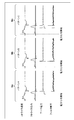
- FIG. 7 shows the result of verifying the arc generation pattern by the arc generation timing control of FIG. 6 by experiment, and it was confirmed that only the pattern generated when the striker 134 was retracted from the cathode target 141 was confirmed.
- the variation in film thickness for each substrate to be processed is reduced as compared with the conventional case by controlling to generate an arc. be able to.
- the form using carbon as the target material has been described.
- the present invention is not limited to carbon, and, for example, Ti or TiN can be used.
Landscapes
- Chemical & Material Sciences (AREA)
- Engineering & Computer Science (AREA)
- Physics & Mathematics (AREA)
- Plasma & Fusion (AREA)
- Analytical Chemistry (AREA)
- Chemical Kinetics & Catalysis (AREA)
- Materials Engineering (AREA)
- Mechanical Engineering (AREA)
- Metallurgy (AREA)
- Organic Chemistry (AREA)
- Physical Vapour Deposition (AREA)
- Manufacturing Of Magnetic Record Carriers (AREA)
Abstract
成膜装置100は、ターゲット部140と、前記ターゲット部から放出された電子が流入するアノード部130と、前記ターゲット部に接触し、前記ターゲット部と前記アノード部を導通させることで、前記ターゲット部と前記アノード部との間にアーク放電を発生させるストライカ134と、前記ストライカを前記ターゲット部の方向または前記ターゲット部から退避する方向へ駆動するストライカ駆動手段134aと、前記ターゲット部と前記アノード部に電力を付与する電力付与手段150と、前記ストライカ駆動手段および前記電力付与手段を制御する制御手段501と、を有し、前記制御手段は、前記ストライカと前記ターゲット部とを接触させた後に、前記ターゲット部と前記アノード部とに電力を付与する。
Description
本発明は、アーク放電を用いた成膜装置に関する。
ハードディスクなどのメディアの保護膜を形成する方法として、C2H2やC2H4などの反応性ガスを利用したCVD法がある。最近では、磁気読取ヘッドとメディアの磁気記録層とのスペーシング距離やヘッド浮上量をより短くしドライブ特性を向上させるため、磁気記録層上に成膜されるカーボンなどの保護膜もより一層薄くすることが求められている。
しかし、CVD法で成膜されるカーボン保護膜は、その特性から2~3nmが限界と言われている。そこで、CVD法に代わる技術として、より薄いカーボン保護膜を形成できるアーク放電を用いた成膜方法(真空アーク成膜法:Vacuum Arc Deposition)が注目されている。真空アーク成膜法では、CVD法に比べて水素含有量が少なく硬いカーボン保護膜を成膜できるため、膜厚を1nm程度まで薄くできる可能性がある。
例えば、特許文献1には、ターゲットにアークスポットを形成してアーク放電によりターゲットイオンおよび電子を放出させるストライカ、アークを維持するためのアノード部、ターゲットの間で電子の流れを作るアノードコイル、ターゲットイオンおよび電子をプロセスチャンバまで誘導するフィルタ部を備える成膜装置が記載されている。
従来の真空アーク成膜法では、図8に示すように、動作開始信号が出力されると(S801)、アーク電源による電力付与を開始すると同時にストライカがターゲットの方向へ移動を開始し(S802)、ストライカがターゲットに接触したことを検知すると(S803)、ストライカが退避位置へ移動を開始する(S804)。この一連の動作のどこかでアークが発生し、アーク電源から付与される電力でアーク放電が維持され、所望の時間に到達したときにアーク電源による電力付与を終了する(S805、S806)。
ここで、従来のアークの発生パターンについて、本願発明者らが検証を行った結果について説明する。図9aから9cは、3つのパターンA~Cにおける、ストライカ速度、ストライカ負荷、アーク電流、フィルタ電流を例示しており、ストライカ速度およびストライカ負荷はストライカ駆動用モータにて測定し、アーク電流はアーク電源にて測定し、フィルタ電流はフィルタ用電源もしくは電流測定手段により測定した結果である。アークの発生は、アークによるプラズマが発生したときに、プラズマからの電子もしくはターゲットイオンがフィルタ部に流入することで発生するフィルタ電流によって確認することができる。本願発明者らは、従来のアークの発生パターンとして3つのパターンA~Cがあることを発見した。すなわち、ストライカがターゲットから退避するときに発生するパターンAと、ストライカがターゲットに接触した直後に発生するパターンBと、ストライカがターゲットに接触した直後に発生するが何かの原因で消滅し、ストライカがターゲットから退避するときに再度発生するパターンCである。アークの発生パターンが複数あるということは被処理基板ごとの膜厚にバラツキが発生するということである。
本発明は、上記課題に鑑みてなされ、その目的は、アークの発生タイミングを制御することにより、被処理物ごとの膜厚のバラツキを従来よりも低減できる成膜装置を実現することである。
上記課題を解決し、目的を達成するために、本発明の成膜装置は、ターゲット部と、前記ターゲット部から放出された電子が流入するアノード部と、前記ターゲット部に接触し、前記ターゲット部と前記アノード部を導通させることで、前記ターゲット部と前記アノード部との間にアーク放電を発生させるストライカと、前記ストライカを前記ターゲット部の方向または前記ターゲット部から退避する方向へ駆動するストライカ駆動手段と、前記ターゲット部と前記アノード部に電力を付与する電力付与手段と、前記ストライカ駆動手段および前記電力付与手段を制御する制御手段と、を有し、前記制御手段は、前記ストライカと前記ターゲット部とを接触させた後に、前記ターゲット部と前記アノード部とに電力を付与する。
本発明によれば、アークの発生するタイミングを制御することにより、被処理物ごとの膜厚のバラツキを従来よりも低減することができる。
本発明のその他の特徴及び利点は、添付図面を参照とした以下の説明により明らかになるであろう。なお、添付図面においては、同じ若しくは同様の構成には、同じ参照番号を付す。
添付図面は明細書に含まれ、その一部を構成し、本発明の実施の形態を示し、その記述と共に本発明の原理を説明するために用いられる。
本発明に係る実施形態の成膜装置の概略構成を示す断面図。
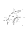
図1の成膜装置のフィルタ部の構成を示す断面図。
図1の成膜装置のソース部の構成を示す2方向から見た側面図。
図1の成膜装置のソース部の構成を示す2方向から見た側面図。
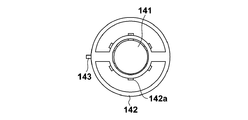
図3BのI-I断面図。
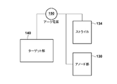
本実施形態の成膜装置の電力供給系の概略構成を示すブロック図。
本実施形態の成膜装置の制御系の概略構成を示すブロック図。
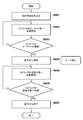
本実施形態の成膜装置におけるアーク発生処理手順を示すフローチャート。
本実施形態の成膜装置によるアーク発生パターンを示す図。
従来の成膜装置におけるアーク発生処理手順を示すフローチャート。
従来の成膜装置によるアーク発生パターンを示す図。
以下、図面を参照して、本発明の好適な実施形態を例示的に詳しく説明する。ただし、この実施の形態に記載されている構成要素はあくまで例示であり、本発明の技術的範囲は、特許請求の範囲によって確定されるのであって、以下の個別の実施形態によって限定されるわけではない。
以下に、本発明の成膜装置を、真空アーク成膜法(Vacuum Arc Deposition)を用いて被処理物としての基板に保護膜を形成する成膜装置に適用した実施形態について説明する。
<装置構成>先ず、図1ないし図3A-Cを参照して、本発明に係る実施形態の成膜装置の構成について説明する。
図1において、本実施形態の成膜装置100は、3nm以下のターゲット材料(例えば、カーボン)の保護膜が成膜される基板1を配置するプロセスチャンバ101と、プロセスチャンバ101に内部で連通するように連結されたフィルタ部110と、フィルタ部110に内部で連通するように連結されたソース部120とを有する。また、プロセスチャンバ101とフィルタ部110、ならびにフィルタ部110とソース部120の各連結部分には絶縁部材2が配置され、各部が電気的絶縁状態を保持するように構成されている。
フィルタ部110は、90°方向に湾曲した誘導路110aを形成し、誘導路11aの内部を真空状態に保持するための1つ以上の輸送管111、輸送管111の大気側または真空側に電子およびターゲットイオンを輸送するための磁場を形成するフィルタコイル112、永久磁石などの磁場形成手段を備える。誘導路110aは1つ以上の輸送管111が連結されて構成され、各輸送管111の外側(大気側)には全周にわたってフィルタコイル112が設けられており、ソース部120で生成された電子およびターゲットイオンを基板1に向けて誘導すると共に、パーティクルとなる粒径の大きいカーボン粒子を除去する。輸送管111には、電圧印加端子113などの電圧印加手段が設けられており、輸送管111が2つ以上のときは各々を電気的に導通状態とするか、各々の連結部分に絶縁部材を配置して電気的絶縁状態とすることが可能であり、いずれかの状態が選択可能である。
ソース部120は、陽極アノード部130と、陰極ターゲット部140と、アノードコイル131aとを備え、陽極アノード部130と陰極ターゲット部140の間での電子電流もしくはイオン電流を維持することによりアーク放電を維持する。
陽極アノード部130は、図3A-Cに詳細を示すように、陽極アノード131、陽極アノード給電部132、陽極アノード給電端子133、ストライカ134、およびアノードハウジング135を有している。
ストライカ134は、陰極ターゲット部140の表面に所定のタイミングで接触することでターゲット表面にアーク放電を発生させる。陰極ターゲット部140上のアークスポットから放出された電子およびターゲットイオンは、プラズマ化してプロセスチャンバ101へ誘導される。陰極ターゲット部140も所定の角度になるように回転駆動される。このように陰極ターゲット部140に対してストライカ134が接触する位置を相対的に移動させることにより、アークスポットの局在化を防止している。なお、アークスポットとはターゲット上でアークが発生している場所のことである。
ストライカ134は、陽極アノード131と同電位とされ、アノードハウジング135は、陽極アノード給電部132と電気的絶縁状態を保持するように絶縁部材2が介装されている。ストライカ134は、ストライカ駆動用モータ134aの駆動力が、ストライカ駆動用モータカップリング134b、ストライカ駆動用モータシャフト134c、ストライカ駆動用モータギヤ134d、ストライカ駆動用モータ動力伝達ギヤ134e、ストライカ給電・駆動シャフト134iを介して伝達されることにより駆動可能に構成されている。また、ストライカ給電端子134g、ストライカ給電部134f、ストライカ給電用ブラシ134hがストライカ給電・駆動シャフト134iに接続されており、ストライカ給電用ブラシ134hがストライカ給電・駆動シャフトに接触するように配置されていることによって、ストライカ134に給電可能となっている。さらに、ストライカ給電・駆動シャフト134iとアノードハウジング135との間には、電気的絶縁状態を保持するように絶縁部材2が介装され、かつ絶縁部材2とストライカ給電・駆動シャフト134iとの間に磁性流体134jを介装することによってストライカ給電・駆動シャフト134iとアノードハウジング135が導通状態にならずにストライカ134の駆動および給電が可能となっている。
また、ストライカ134は、アーム部134kとチップ部134lからなり、高温・大電流に対する耐久性のある材質が望ましい。例えば、アーム部134kをモリブデン製、チップ部134lをグラファイト製とする。また、アーム部とチップ部を一体的に構成しても良い。
陰極ターゲット部140は、円筒状または円盤状のカーボングラファイト製の陰極ターゲット141、陰極ターゲット給電部142、陰極ターゲット給電端子143、陰極ターゲットハウジング144を有している。陰極ターゲット141は、陰極ターゲット回転用モータ141aの駆動力が、陰極ターゲット回転用モータカップリング141b、陰極ターゲット回転用モータシャフト141c、陰極ターゲット回転用モータギヤ141d、陰極ターゲット回転用モータ動力伝達ギヤ141e、陰極ターゲット回転用シャフト141f、陰極ターゲットブラケット141hを介して伝達されることにより回転可能に構成されている。また、陰極ターゲット141は、陰極ターゲット給電部142、陰極ターゲット給電用ブラシ142a、陰極ターゲット給電端子143と接続されていることにより給電可能に構成されている。さらにまた、陰極ターゲット回転用シャフト141fと陰極ターゲットハウジング144との間には、電気的絶縁状態を保持するように絶縁部材2が介装され、かつ絶縁部材2と陰極ターゲット回転用シャフト141fとの間に磁性流体141gを介装することによって陰極ターゲット回転用シャフト141fと陰極ターゲットハウジング144が導通状態にならずに陰極ターゲット141の回転および給電が可能となっている。
上記構成において、ストライカ134と陰極ターゲット141が接触するときに陽極アノード131と陰極ターゲット141が短絡し、アークが発生する。
不図示のアーク電源から陰極ターゲット141に負の電圧を印加し、ストライカ134及び陽極アノード131に正の電圧を印加することで、アノードコイル131aによる磁場に沿って陰極ターゲット141と陽極アノード131との間で電子の流れを形成する。
アークスポットで発生した電子は、アーク維持電子とイオン輸送電子となる。アーク維持電子は、ターゲット表面で発生した電子の一部をアノードコイル131aの磁場で誘導されて陽極アノード131へ流入する電子であり、陰極ターゲット141で発生したプラズマアークを維持するために、陰極ターゲット141と陽極アノード部131の間に電流を流してアークスポットを加熱することに利用される。
イオン輸送電子は、ターゲットイオンを被処理基板1に到達させるための電子であり、電子のクーロン力を利用してイオンを引っ張る働きをする。イオン輸送電子はフィルタ部110により作られた磁場により被処理基板1の方向へ誘導される。
上記構成によって、プロセスチャンバ101内部で被処理基板1の表面にターゲットイオンを付着・堆積させて保護膜が成膜される。
<電力供給系>次に、図4も参照して、本実施形態の成膜装置の電力供給系の構成について説明する。
プロセスチャンバ101は、アースに接続されている。フィルタ部110は、電圧印加端子113を介して不図示のフィルタ電源または電流測定部に接続されている。陽極アノード部130は、陽極アノード給電端子133を介してアーク電源150に接続されている。ストライカ134は、ストライカ給電端子134gを介してアーク電源150に接続されている。陰極ターゲット部140は、陰極ターゲット給電端子143を介してアーク電源150の負電極側に接続されている。陽極アノード部130とストライカ134は同電位になるようにアーク電源150のプラス側に接続されており、陰極ターゲット部140はアーク電源150のマイナス側に接続されている。また、アーク電源150は電流の通電制御の方が望ましいが、電圧の印加制御であっても良い。本明細書中では、電流と電圧を総称して電力と呼ぶものとする。
なお、陽極アノード部130側と陰極ターゲット部140の間に電位差を生じさせる回路であれば、陽極アノード部130側と陰極ターゲット部140の間でアーク放電が生じるため、複数の電源を用いて回路を構成しても良い。例えば、第1の電源の一端をアースに、他端を陽極アノード部130側にそれぞれ接続し、第2電源の一端を陰極ターゲット部140に、他端をアースに接続する回路であってもよい。
本実施形態のストライカ134は、陽極アノード部130と並列にアーク電源150に接続されているが、ストライカ134を陽極アノード部130に接続する直列的な配線でも良い。さらに、ストライカ134と陽極アノード部130に供給される電力が実質的に同じであれば、ストライカ134に電力を供給する電源と、陽極アノード部130に電力を供給する電源を別個にしても良い。本実施形態において、アークの発生させる際に、陽極アノード部130に電力を供給するときはストライカ134にも同様に電力が供給されるものとする。
<制御系>次に、図5を参照して、本実施形態の成膜装置の制御系の概略構成について説明する。
図5に示すように、本実施形態の成膜装置は、装置全体を統括して制御するメイン制御装置500と、アークの発生を制御するアーク制御装置501とを有する。メイン制御装置500およびアーク制御装置501は、メモリ等の記憶部やCPU等の演算処理部、通信部を有する。アーク制御装置501は、メイン制御装置500から受けた制御信号に従って電力付与装置503としてのアーク電源150による電力供給を制御すると共に、ストライカ駆動装置504としてのモータ134a、141aの回転を制御する。なお、電力付与装置503は、ストライカ134と陰極ターゲット部140の間の抵抗値を測定するための抵抗計を含む。また、ストライカ駆動装置504は、ストライカ駆動用モータ134aや陰極ターゲット部140の陰極ターゲット回転用モータ141aの回転数やトルクを検知するエンコーダ等のセンサを含む。
<アーク発生タイミングの制御処理>次に、図6を参照して、本実施形態の成膜装置によるアーク発生タイミングの制御処理について説明する。
メイン制御装置500から動作開始信号が出力されると(S601)、アーク制御装置501による処理が開始される。ここで、動作開始信号が出力されてもアーク電源150は電力付与を開始せず、ストライカ134の陰極ターゲット141と接触する方向への駆動が開始される(S602)。
その後、ストライカ134が陰極ターゲット141に接触したことを検知すると(S603)、アーク制御装置501はアーク電源150による電力付与を開始する(604)。
その後、ストライカ134の陰極ターゲット141から退避する方向への駆動が開始される(S605)。
ストライカ134が、退避位置へ到達したことを検知すると(S606)、アーク制御装置501はアーク電源150による電力付与を停止する(S607)。
上記動作を被処理基板ごとに繰り返し行う。
なお、ストライカ134と陰極ターゲット141との接触は、ストライカ134が受ける反力による負荷を検知することで判定できる。つまり、ストライカ駆動用モータ134aの負荷が所定閾値を超えたときにストライカ134と陰極ターゲット141が接触したと判定される。
他の方法として、ストライカ134の移動速度が所定閾値以下になったとき、または、ストライカ134と陰極ターゲット141の間の電気抵抗値が所定閾値以下になったときに、ストライカ134と陰極ターゲット141が接触したと判定することもできる。
また、本実施形態では、ストライカ134がターゲット141に接触した後、電力付与を開始し、ストライカ134を退避させているが、ストライカ134がターゲット141に接触している状態から非接触状態となるまでの間に電力付与を行っても良い。また、ストライカ134とターゲット141が接触してから、一定の時間経過後にストライカ134の退避位置への駆動を開始しても良い。
図7は、図6のアーク発生タイミング制御によるアーク発生パターンを実験により検証した結果を示し、ストライカ134が陰極ターゲット141から退避するときに発生するパターンのみであることが確認された。
以上説明したように、本実施形態によれば、ストライカと陰極ターゲットとを接触させた後に、アークを発生させるように制御することにより、被処理基板ごとの膜厚のバラツキを従来よりも低減することができる。
なお、上述した実施形態では、ターゲット材料としてカーボンを用いた形態について記載したが、カーボンに限らず、例えば、TiやTiNを用いることも可能である。
本発明は上記実施の形態に制限されるものではなく、本発明の精神及び範囲から離脱することなく、様々な変更及び変形が可能である。従って、本発明の範囲を公にするために、以下の請求項を添付する。
本願は、2013年5月23日提出の日本国特許出願特願2013-109378を基礎として優先権を主張するものであり、その記載内容の全てを、ここに援用する。
Claims (7)
- ターゲット部と、
前記ターゲット部から放出された電子が流入するアノード部と、
前記ターゲット部に接触し、前記ターゲット部と前記アノード部を導通させることで、前記ターゲット部と前記アノード部との間にアーク放電を発生させるストライカと、
前記ストライカを前記ターゲット部の方向または前記ターゲット部から退避する方向へ駆動するストライカ駆動手段と、
前記ターゲット部と前記アノード部に電力を付与する電力付与手段と、
前記ストライカ駆動手段および前記電力付与手段を制御する制御手段と、を有し、
前記制御手段は、前記ストライカと前記ターゲット部とを接触させた後に、前記ターゲット部と前記アノード部とに電力を付与することを特徴とする成膜装置。 - 前記制御手段は、前記ストライカが前記ターゲット部に接触している状態から非接触状態となるまでの間に、前記電力付与手段により電力を付与することを特徴とする請求項1に記載の成膜装置。
- 前記制御手段は、前記ストライカへの負荷が所定閾値を超えたときに、前記ストライカが前記ターゲット部に接触したと判定することを特徴とする請求項1または2に記載の成膜装置。
- 前記制御手段は、前記ストライカと前記ターゲット部の間の抵抗値が所定閾値以下となったきに、前記ストライカが前記ターゲット部に接触したと判定することを特徴とする請求項1または2に記載の成膜装置。
- 前記制御手段は、前記ストライカの移動速度が所定閾値以下となったときに、前記ストライカが前記ターゲット部に接触したと判定することを特徴とする請求項1または2に記載の成膜装置。
- 前記電力付与手段は、電流を通電させるか、電圧を印加することで電力を付与することを特徴とする請求項1ないし5のいずれか1項に記載の成膜装置。
- 前記アノード部に連結されて、前記ターゲット部から放出された電子を被処理物の方向へ誘導するフィルタ部を更に有することを特徴とする請求項1乃至6のいずれか1項に記載の成膜装置。
Priority Applications (4)
| Application Number | Priority Date | Filing Date | Title |
|---|---|---|---|
| JP2015518047A JP5965058B2 (ja) | 2013-05-23 | 2014-02-07 | 成膜装置 |
| SG11201509066UA SG11201509066UA (en) | 2013-05-23 | 2014-02-07 | Deposition apparatus |
| TW103117770A TWI526567B (zh) | 2013-05-23 | 2014-05-21 | Film forming device |
| US14/938,513 US10011899B2 (en) | 2013-05-23 | 2015-11-11 | Deposition apparatus |
Applications Claiming Priority (2)
| Application Number | Priority Date | Filing Date | Title |
|---|---|---|---|
| JP2013-109378 | 2013-05-23 | ||
| JP2013109378 | 2013-05-23 |
Related Child Applications (1)
| Application Number | Title | Priority Date | Filing Date |
|---|---|---|---|
| US14/938,513 Continuation US10011899B2 (en) | 2013-05-23 | 2015-11-11 | Deposition apparatus |
Publications (1)
| Publication Number | Publication Date |
|---|---|
| WO2014188634A1 true WO2014188634A1 (ja) | 2014-11-27 |
Family
ID=51933209
Family Applications (1)
| Application Number | Title | Priority Date | Filing Date |
|---|---|---|---|
| PCT/JP2014/000676 Ceased WO2014188634A1 (ja) | 2013-05-23 | 2014-02-07 | 成膜装置 |
Country Status (5)
| Country | Link |
|---|---|
| US (1) | US10011899B2 (ja) |
| JP (1) | JP5965058B2 (ja) |
| SG (1) | SG11201509066UA (ja) |
| TW (1) | TWI526567B (ja) |
| WO (1) | WO2014188634A1 (ja) |
Cited By (1)
| Publication number | Priority date | Publication date | Assignee | Title |
|---|---|---|---|---|
| EP3388547A4 (en) * | 2016-01-26 | 2019-08-14 | Kabushiki Kaisha Kobe Seiko Sho (Kobe Steel, Ltd.) | ARC EVAPORATION DEVICE |
Families Citing this family (1)
| Publication number | Priority date | Publication date | Assignee | Title |
|---|---|---|---|---|
| JP6350603B2 (ja) * | 2016-07-07 | 2018-07-04 | トヨタ自動車株式会社 | アーク放電発生装置及び成膜方法 |
Citations (4)
| Publication number | Priority date | Publication date | Assignee | Title |
|---|---|---|---|---|
| JP2002241927A (ja) * | 2001-02-20 | 2002-08-28 | Shimadzu Corp | 陰極アーク放電を用いた成膜装置 |
| JP2004211127A (ja) * | 2002-12-27 | 2004-07-29 | Nissin Electric Co Ltd | 真空アーク蒸着装置 |
| JP2004218087A (ja) * | 2003-01-10 | 2004-08-05 | Nanofilm Technologies Internatl Pte Ltd | 銅配線 |
| JP2007254770A (ja) * | 2006-03-20 | 2007-10-04 | Fujitsu Ltd | 成膜方法及び成膜装置 |
Family Cites Families (3)
| Publication number | Priority date | Publication date | Assignee | Title |
|---|---|---|---|---|
| GB9503305D0 (en) * | 1995-02-20 | 1995-04-12 | Univ Nanyang | Filtered cathodic arc source |
| KR100230279B1 (ko) * | 1997-03-31 | 1999-11-15 | 윤종용 | 음극 아크 방전을 이용한 박막 증착장치 |
| WO2008136174A1 (ja) | 2007-04-13 | 2008-11-13 | Shinmaywa Industries, Ltd. | 成膜装置 |
-
2014
- 2014-02-07 JP JP2015518047A patent/JP5965058B2/ja active Active
- 2014-02-07 WO PCT/JP2014/000676 patent/WO2014188634A1/ja not_active Ceased
- 2014-02-07 SG SG11201509066UA patent/SG11201509066UA/en unknown
- 2014-05-21 TW TW103117770A patent/TWI526567B/zh active
-
2015
- 2015-11-11 US US14/938,513 patent/US10011899B2/en active Active
Patent Citations (4)
| Publication number | Priority date | Publication date | Assignee | Title |
|---|---|---|---|---|
| JP2002241927A (ja) * | 2001-02-20 | 2002-08-28 | Shimadzu Corp | 陰極アーク放電を用いた成膜装置 |
| JP2004211127A (ja) * | 2002-12-27 | 2004-07-29 | Nissin Electric Co Ltd | 真空アーク蒸着装置 |
| JP2004218087A (ja) * | 2003-01-10 | 2004-08-05 | Nanofilm Technologies Internatl Pte Ltd | 銅配線 |
| JP2007254770A (ja) * | 2006-03-20 | 2007-10-04 | Fujitsu Ltd | 成膜方法及び成膜装置 |
Cited By (2)
| Publication number | Priority date | Publication date | Assignee | Title |
|---|---|---|---|---|
| EP3388547A4 (en) * | 2016-01-26 | 2019-08-14 | Kabushiki Kaisha Kobe Seiko Sho (Kobe Steel, Ltd.) | ARC EVAPORATION DEVICE |
| US10844473B2 (en) | 2016-01-26 | 2020-11-24 | Kobe Steel, Ltd. | Arc evaporation device |
Also Published As
| Publication number | Publication date |
|---|---|
| JP5965058B2 (ja) | 2016-08-03 |
| SG11201509066UA (en) | 2015-12-30 |
| TWI526567B (zh) | 2016-03-21 |
| US20160060750A1 (en) | 2016-03-03 |
| US10011899B2 (en) | 2018-07-03 |
| JPWO2014188634A1 (ja) | 2017-02-23 |
| TW201506194A (zh) | 2015-02-16 |
Similar Documents
| Publication | Publication Date | Title |
|---|---|---|
| JP4951477B2 (ja) | 電子放出源 | |
| CN107435135B (zh) | 溅射装置及使用该溅射装置的溅射方法 | |
| US8094428B2 (en) | Wafer grounding methodology | |
| JP5965058B2 (ja) | 成膜装置 | |
| JP2015067839A (ja) | 成膜装置 | |
| JP5095524B2 (ja) | プラズマcvd装置及び磁気記録媒体の製造方法 | |
| CN1495283A (zh) | 匹配箱、使用匹配箱的真空装置及真空处理方法 | |
| KR20200114826A (ko) | 매엽식 건식 식각 챔버 | |
| US20230162996A1 (en) | Etching apparatus | |
| JP5764789B2 (ja) | プラズマcvd装置及び磁気記録媒体の製造方法 | |
| CN108495948B (zh) | 电弧蒸发装置 | |
| JP6967965B2 (ja) | コロナシールドテープ及び当該コロナシールドテープを備える電気機械 | |
| JP2009088558A (ja) | 静電チャック装置 | |
| JP2017226870A (ja) | 真空アーク蒸着装置および被膜の形成方法 | |
| JP4410700B2 (ja) | 走査形プローブ顕微鏡 | |
| TW202103200A (zh) | 負離子生成裝置 | |
| US12606914B2 (en) | Electrode filament connection member, chemical vapor deposition apparatus, and method for manufacturing recording medium substrate | |
| KR20190140522A (ko) | 다중 노즐을 구비한 고능률 금속 3d 아크 프린터 | |
| JP2015125922A (ja) | 電子放出素子および電子放出装置 | |
| JP2019163531A (ja) | 負イオン生成装置 | |
| TWI700967B (zh) | 負離子生成裝置 | |
| JP5342364B2 (ja) | 給電機構および真空処理装置 | |
| Anuraga et al. | A contribution to breakdown voltage characteristics in air for inter-electrode distances 1–10 μm at various pressures | |
| JP2012136758A (ja) | 基板処理装置 | |
| CN116896006A (zh) | 负离子生成装置 |
Legal Events
| Date | Code | Title | Description |
|---|---|---|---|
| 121 | Ep: the epo has been informed by wipo that ep was designated in this application |
Ref document number: 14800603 Country of ref document: EP Kind code of ref document: A1 |
|
| ENP | Entry into the national phase |
Ref document number: 2015518047 Country of ref document: JP Kind code of ref document: A |
|
| NENP | Non-entry into the national phase |
Ref country code: DE |
|
| 122 | Ep: pct application non-entry in european phase |
Ref document number: 14800603 Country of ref document: EP Kind code of ref document: A1 |