WO2014185459A1 - 送信装置及び送信方法 - Google Patents
送信装置及び送信方法 Download PDFInfo
- Publication number
- WO2014185459A1 WO2014185459A1 PCT/JP2014/062865 JP2014062865W WO2014185459A1 WO 2014185459 A1 WO2014185459 A1 WO 2014185459A1 JP 2014062865 W JP2014062865 W JP 2014062865W WO 2014185459 A1 WO2014185459 A1 WO 2014185459A1
- Authority
- WO
- WIPO (PCT)
- Prior art keywords
- signal
- power
- output
- band
- transmission
- Prior art date
- Legal status (The legal status is an assumption and is not a legal conclusion. Google has not performed a legal analysis and makes no representation as to the accuracy of the status listed.)
- Ceased
Links
Images










Classifications
-
- H—ELECTRICITY
- H03—ELECTRONIC CIRCUITRY
- H03F—AMPLIFIERS
- H03F3/00—Amplifiers with only discharge tubes or only semiconductor devices as amplifying elements
- H03F3/20—Power amplifiers, e.g. Class B amplifiers, Class C amplifiers
- H03F3/21—Power amplifiers, e.g. Class B amplifiers, Class C amplifiers with semiconductor devices only
- H03F3/211—Power amplifiers, e.g. Class B amplifiers, Class C amplifiers with semiconductor devices only using a combination of several amplifiers
-
- H—ELECTRICITY
- H03—ELECTRONIC CIRCUITRY
- H03F—AMPLIFIERS
- H03F1/00—Details of amplifiers with only discharge tubes, only semiconductor devices or only unspecified devices as amplifying elements
- H03F1/02—Modifications of amplifiers to raise the efficiency, e.g. gliding Class A stages, use of an auxiliary oscillation
- H03F1/0205—Modifications of amplifiers to raise the efficiency, e.g. gliding Class A stages, use of an auxiliary oscillation in transistor amplifiers
- H03F1/0277—Selecting one or more amplifiers from a plurality of amplifiers
-
- H—ELECTRICITY
- H03—ELECTRONIC CIRCUITRY
- H03F—AMPLIFIERS
- H03F3/00—Amplifiers with only discharge tubes or only semiconductor devices as amplifying elements
- H03F3/189—High-frequency amplifiers, e.g. radio frequency amplifiers
- H03F3/19—High-frequency amplifiers, e.g. radio frequency amplifiers with semiconductor devices only
-
- H—ELECTRICITY
- H03—ELECTRONIC CIRCUITRY
- H03F—AMPLIFIERS
- H03F3/00—Amplifiers with only discharge tubes or only semiconductor devices as amplifying elements
- H03F3/20—Power amplifiers, e.g. Class B amplifiers, Class C amplifiers
- H03F3/24—Power amplifiers, e.g. Class B amplifiers, Class C amplifiers of transmitter output stages
- H03F3/245—Power amplifiers, e.g. Class B amplifiers, Class C amplifiers of transmitter output stages with semiconductor devices only
-
- H—ELECTRICITY
- H03—ELECTRONIC CIRCUITRY
- H03F—AMPLIFIERS
- H03F3/00—Amplifiers with only discharge tubes or only semiconductor devices as amplifying elements
- H03F3/60—Amplifiers in which coupling networks have distributed constants, e.g. with waveguide resonators
- H03F3/602—Combinations of several amplifiers
-
- H—ELECTRICITY
- H03—ELECTRONIC CIRCUITRY
- H03F—AMPLIFIERS
- H03F3/00—Amplifiers with only discharge tubes or only semiconductor devices as amplifying elements
- H03F3/72—Gated amplifiers, i.e. amplifiers which are rendered operative or inoperative by means of a control signal
-
- H—ELECTRICITY
- H04—ELECTRIC COMMUNICATION TECHNIQUE
- H04B—TRANSMISSION
- H04B1/00—Details of transmission systems, not covered by a single one of groups H04B3/00 - H04B13/00; Details of transmission systems not characterised by the medium used for transmission
- H04B1/005—Details of transmission systems, not covered by a single one of groups H04B3/00 - H04B13/00; Details of transmission systems not characterised by the medium used for transmission adapting radio receivers, transmitters andtransceivers for operation on two or more bands, i.e. frequency ranges
-
- H—ELECTRICITY
- H03—ELECTRONIC CIRCUITRY
- H03F—AMPLIFIERS
- H03F1/00—Details of amplifiers with only discharge tubes, only semiconductor devices or only unspecified devices as amplifying elements
- H03F1/02—Modifications of amplifiers to raise the efficiency, e.g. gliding Class A stages, use of an auxiliary oscillation
- H03F1/0205—Modifications of amplifiers to raise the efficiency, e.g. gliding Class A stages, use of an auxiliary oscillation in transistor amplifiers
- H03F1/0288—Modifications of amplifiers to raise the efficiency, e.g. gliding Class A stages, use of an auxiliary oscillation in transistor amplifiers using a main and one or several auxiliary peaking amplifiers whereby the load is connected to the main amplifier using an impedance inverter, e.g. Doherty amplifiers
-
- H—ELECTRICITY
- H03—ELECTRONIC CIRCUITRY
- H03F—AMPLIFIERS
- H03F1/00—Details of amplifiers with only discharge tubes, only semiconductor devices or only unspecified devices as amplifying elements
- H03F1/02—Modifications of amplifiers to raise the efficiency, e.g. gliding Class A stages, use of an auxiliary oscillation
- H03F1/04—Modifications of amplifiers to raise the efficiency, e.g. gliding Class A stages, use of an auxiliary oscillation in discharge-tube amplifiers
- H03F1/06—Modifications of amplifiers to raise the efficiency, e.g. gliding Class A stages, use of an auxiliary oscillation in discharge-tube amplifiers to raise the efficiency of amplifying modulated radio frequency waves; to raise the efficiency of amplifiers acting also as modulators
- H03F1/07—Doherty-type amplifiers
-
- H—ELECTRICITY
- H03—ELECTRONIC CIRCUITRY
- H03F—AMPLIFIERS
- H03F2200/00—Indexing scheme relating to amplifiers
- H03F2200/111—Indexing scheme relating to amplifiers the amplifier being a dual or triple band amplifier, e.g. 900 and 1800 MHz, e.g. switched or not switched, simultaneously or not
-
- H—ELECTRICITY
- H03—ELECTRONIC CIRCUITRY
- H03F—AMPLIFIERS
- H03F2200/00—Indexing scheme relating to amplifiers
- H03F2200/39—Different band amplifiers are coupled in parallel to broadband the whole amplifying circuit
-
- H—ELECTRICITY
- H03—ELECTRONIC CIRCUITRY
- H03F—AMPLIFIERS
- H03F2200/00—Indexing scheme relating to amplifiers
- H03F2200/451—Indexing scheme relating to amplifiers the amplifier being a radio frequency amplifier
-
- H—ELECTRICITY
- H03—ELECTRONIC CIRCUITRY
- H03F—AMPLIFIERS
- H03F2200/00—Indexing scheme relating to amplifiers
- H03F2200/541—Transformer coupled at the output of an amplifier
-
- H—ELECTRICITY
- H03—ELECTRONIC CIRCUITRY
- H03F—AMPLIFIERS
- H03F2203/00—Indexing scheme relating to amplifiers with only discharge tubes or only semiconductor devices as amplifying elements covered by H03F3/00
- H03F2203/20—Indexing scheme relating to power amplifiers, e.g. Class B amplifiers, Class C amplifiers
- H03F2203/21—Indexing scheme relating to power amplifiers, e.g. Class B amplifiers, Class C amplifiers with semiconductor devices only
- H03F2203/211—Indexing scheme relating to power amplifiers, e.g. Class B amplifiers, Class C amplifiers with semiconductor devices only using a combination of several amplifiers
- H03F2203/21142—Output signals of a plurality of power amplifiers are parallel combined to a common output
-
- H—ELECTRICITY
- H03—ELECTRONIC CIRCUITRY
- H03F—AMPLIFIERS
- H03F2203/00—Indexing scheme relating to amplifiers with only discharge tubes or only semiconductor devices as amplifying elements covered by H03F3/00
- H03F2203/20—Indexing scheme relating to power amplifiers, e.g. Class B amplifiers, Class C amplifiers
- H03F2203/21—Indexing scheme relating to power amplifiers, e.g. Class B amplifiers, Class C amplifiers with semiconductor devices only
- H03F2203/211—Indexing scheme relating to power amplifiers, e.g. Class B amplifiers, Class C amplifiers with semiconductor devices only using a combination of several amplifiers
- H03F2203/21157—A filter circuit being added at the output of a power amplifier stage
-
- H—ELECTRICITY
- H03—ELECTRONIC CIRCUITRY
- H03F—AMPLIFIERS
- H03F2203/00—Indexing scheme relating to amplifiers with only discharge tubes or only semiconductor devices as amplifying elements covered by H03F3/00
- H03F2203/72—Indexing scheme relating to gated amplifiers, i.e. amplifiers which are rendered operative or inoperative by means of a control signal
- H03F2203/7209—Indexing scheme relating to gated amplifiers, i.e. amplifiers which are rendered operative or inoperative by means of a control signal the gated amplifier being switched from a first band to a second band
-
- H—ELECTRICITY
- H03—ELECTRONIC CIRCUITRY
- H03F—AMPLIFIERS
- H03F2203/00—Indexing scheme relating to amplifiers with only discharge tubes or only semiconductor devices as amplifying elements covered by H03F3/00
- H03F2203/72—Indexing scheme relating to gated amplifiers, i.e. amplifiers which are rendered operative or inoperative by means of a control signal
- H03F2203/7215—Indexing scheme relating to gated amplifiers, i.e. amplifiers which are rendered operative or inoperative by means of a control signal the gated amplifier being switched on or off by a switch at the input of the amplifier
-
- H—ELECTRICITY
- H03—ELECTRONIC CIRCUITRY
- H03F—AMPLIFIERS
- H03F2203/00—Indexing scheme relating to amplifiers with only discharge tubes or only semiconductor devices as amplifying elements covered by H03F3/00
- H03F2203/72—Indexing scheme relating to gated amplifiers, i.e. amplifiers which are rendered operative or inoperative by means of a control signal
- H03F2203/7236—Indexing scheme relating to gated amplifiers, i.e. amplifiers which are rendered operative or inoperative by means of a control signal the gated amplifier being switched on or off by putting into parallel or not, by choosing between amplifiers by (a ) switch(es)
Definitions
- the present invention is based on the priority claim of Japanese patent application: Japanese Patent Application No. 2013-103931 (filed on May 16, 2013), the entire contents of which are incorporated herein by reference. Shall.
- the present invention relates to a transmission device and a transmission method.
- the present invention relates to a transmission apparatus and a transmission method for transmitting RF (Radio Frequency) signals used in wireless communication and arranged in a plurality of bands.
- RF Radio Frequency
- the power amplifier (PA; Power Amp) of the transmission signal used in the wireless communication device has high power consumption among the components of the wireless communication device. Therefore, improving the power efficiency of the power amplifier is a high priority requirement in the development of wireless communication devices.
- linear modulation is mainly used to improve spectrum efficiency. Linear modulation has a high demand for signal distortion. Therefore, in order to maintain the linearity in the power amplifier, the average output power is set to a value lower than the saturated output power so that the instantaneous maximum output (peak) power becomes equal to or lower than the saturated output.
- the ratio (power efficiency) between the DC (direct current) supply power to the power amplifier and the extracted transmission power decreases.
- the reduction in power efficiency is not acceptable from the viewpoint of power saving.
- Patent Literature 1 and Non-Patent Literature 1 among the plurality of power amplifiers, the amplitude of the RF signal input to the power amplifier bearing the least significant bit (LSB) is continuously (analogously) controlled.
- a control method for correcting a quantization error generated from another power amplifier is disclosed.
- Patent Document 2 by continuously controlling the power supply voltage of the power amplifier responsible for LSB (analog), the output power of the power amplifier is continuously adjusted so as to correct the quantization error generated from other power amplifiers.
- a technique for controlling in an analog manner is disclosed.
- Non-Patent Document 2 discloses a transmission device that digitally controls transmission power of a power amplifier using a ⁇ / 4 line.
- Non-Patent Document 3 discloses a ⁇ / 4 line that can be used as an output combining element.
- the transmitting apparatus 200-1 shown in FIG. 20 transmits an RF signal 34 of band 1 (carrier frequency f1).
- the transmitting apparatus 200-2 transmits an RF signal 35 of band 2 (carrier frequency f2).
- FIG. 20 by using two transmission apparatuses 200-1 and 200-2, it is possible to cope with dual band (two-band transmission).
- the number of bands that can be handled in proportion to the number of transmission apparatuses increases, so if three or more transmission apparatuses are arranged, transmission of three or more bands is possible.
- an output combining element (for example, for example) that synthesizes waveforms output from a plurality of power amplifiers arranged therein in proportion to the number of bands (that is, the number of transmission devices).
- the number of transformer elements increases.
- the number of output combining elements that are twice the number of output combining elements included in one transmission device is required for the entire apparatus.
- the number of necessary power amplifiers also increases in proportion to the number of bands.
- the size of the output combining element is large, and problems occur when the transmission device is multibanded.
- the output combining element is mounted as a discrete component, the size of the transmission apparatus increases as the number of output combining elements increases.
- the output synthesis element is mounted on an IC (IntegratedIntegrCircuit), the area and cost of the IC increase as the number of output synthesis elements increases.
- the present invention provides a transmission apparatus and a transmission method that contribute to realizing power saving while suppressing an increase in the number of output combining elements when the transmission apparatus is multiband. With the goal.
- a plurality of amplifying units for amplifying RF signals arranged in at least two or more bands, and a plurality of amplifying units according to the total power of the RF signals to be transmitted In accordance with the power ratio for each band of the RF signal to be transmitted and the first control unit that selects the amplification unit that performs the amplification operation, the total power of the input RF signal is constant in each of the selected amplification units And a second control unit that changes the power ratio of the RF signal for each band, and a synthesis unit that synthesizes the RF signal output from the selected amplification unit.
- Amplifying step for amplifying a signal a first control step for selecting an amplifying unit for performing an amplifying operation among the plurality of amplifying units according to the total power of the RF signal to be transmitted, A second control step of changing the power ratio of the RF signal for each band while keeping the power sum of the input RF signal constant in each of the selected amplifiers according to the power ratio of And a synthesizing step of synthesizing the RF signals output from the selected amplifying unit.
- this method is linked to a specific machine called an amplification unit that amplifies an RF signal.
- a transmission apparatus and a transmission method that contribute to realizing power saving while suppressing an increase in the number of output combining elements when a transmission apparatus is multibanded.
- FIG. 4 is a flowchart illustrating an example of an operation of a transmission device 10.
- 6 is a diagram illustrating an example of a voltage amplitude waveform of band 1 output to a load 15 of the transmission device 10.
- FIG. 6 is a diagram illustrating the number n of power amplifiers 11 to be operated and the amount of signal distortion of band 1 output to a load 15 when a WCDMA (registered trademark) -DL signal is transmitted in band 1.
- FIG. 7 is a diagram illustrating the number n of power amplifiers 11 to be operated and the amount of signal distortion in band 2 output to a load 15 when a WCDMA-DL signal is transmitted in band 2.
- FIG. It is a figure which shows an example of the circuit structure of the transmitter 200 which digitally controls the transmission power of a power amplifier.
- 6 is a diagram illustrating an example of a voltage amplitude waveform output to a load 15 of a transmission device 200.
- FIG. 6 is a diagram illustrating the number n of power amplifiers 11 to be operated and the amount of signal distortion of a signal output to a load 15 when a transmitting apparatus 200 transmits a WCDMA-DL signal.
- the transmission apparatus 100 shown in FIG. 1 performs an amplification operation among the plurality of amplification units 101 that amplifies the RF signals arranged in at least two or more bands and the total power of the RF signals to be transmitted.
- the power sum of the input RF signal is held constant in each of the selected amplification units 101.
- the second control unit 103 that changes the power ratio of the RF signal for each band, and the synthesis unit 104 that synthesizes the RF signal output from the selected amplification unit 101 are provided.
- the transmission apparatus 100 uses the first control unit 102 to control the output power sum of the RF signals to be transmitted discretely (digitally), thereby reducing power consumption. Further, the second control unit 103 performs control to keep the total power of the input RF signal constant so that each of the selected amplification units 101 performs a saturation operation.
- the RF signals can be amplified with high power efficiency in each amplifying unit 101. That is, in each amplification unit 101, the power sum of the RF signals arranged in a plurality of bands is set to a constant value (for example, saturated output power), so that the power consumption of the transmission device 100 is kept low while the transmission device 100 Multibanding can be realized.
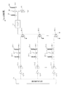
- FIG. 2 is a diagram illustrating a circuit configuration of the transmission apparatus 10 according to the first embodiment.
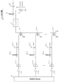
- the transmission apparatus 10 includes a plurality of power amplifiers 11-1 to 11-n, a plurality of switches 12-1 to 12-n, a plurality of transformer elements 13-1 to 13-n, and a filter. 14, a load 15, and a signal generation control unit 16.
- n is a positive integer, and the same applies in the following description.
- the outputs of the plurality of power amplifiers 11 are combined by the transformer element 13.
- the combined output of the power amplifier 11 combined by the transformer element 13 is output from the antenna as the load 15 via the filter 14.
- the transmission apparatus 10 includes a combining unit including a plurality of power amplifiers 11 and the same number of transformer elements 13. The primary side of each transformer element 13 and the corresponding power amplifier 11 are connected, and the secondary side of the transformer element 13 is connected in series.
- the signal generation control unit 16 serves as a modulation unit that modulates transmission data supplied from a higher-level signal source (not shown) connected to the transmission apparatus 10 using carrier waves included in two bands. , RF signals arranged in a plurality of bands are generated.
- the signal generation control unit 16 outputs RF signals included in two bands to each of the power amplifiers 11.
- Each RF signal is amplified by the power amplifier 11 and output to the corresponding transformer element 13. That is, the transmission device 10 includes a plurality of power amplifiers 11 that amplify RF signals arranged in at least two bands.
- the RF signal 20-i of band 1 (carrier frequency f1) and the RF signal of band 2 (carrier frequency f2) are transmitted from the power amplifier 11-i (i is an integer from 1 to n, the same applies hereinafter). Signals 21-i are respectively output.
- the band 1 RF signal 20-i output from the power amplifier 11-i is combined with another RF signal in the transformer element 13, and is output to the load 15 as a combined RF signal 31 of band 1 through the filter 14. .
- the band 2 RF signal 21-i output from the power amplifier 11-i is combined with another RF signal in the transformer element 13 and output to the load 15 as a combined RF signal 32 of band 2 via the filter 14. Is done.
- each power amplifier 11 is always controlled to be in an on state in which saturated output power is output or in an off state in which power is not output. That is, the signal generation control unit 16 controls the output power to the load 15 discretely (digitally) by selecting the power amplifier 11 to be operated from the plurality of power amplifiers 11.
- a switch 12 installed between the signal generation control unit 16 and the input terminal of the power amplifier 11 is used.
- the signal generation control unit 16 and the switch 12 are connected by a control line (not shown), and the on / off state of the switch 12 can be switched from the signal generation control unit 16.
- the signal generation control unit 16 selects a power amplifier 11 that performs an amplification operation from among the plurality of power amplifiers 11 by switching on / off of the switch 12 according to the total power of the RF signal to be transmitted. Take control. In addition, the signal generation control unit 16 keeps the total power of the input RF signal constant in each of the selected power amplifiers 11 according to the power ratio of each RF signal to be transmitted for each band, Second control for changing the power ratio of the RF signal is performed. The signal generation control unit 16 combines the first control and the second control, thereby suppressing the quantization error to a desired value or less while supporting multiband wireless communication, and reducing the power consumption of the transmission device 10. Is realized.
- the signal generation control unit 16 has two outputs, that is, discrete output power control by selecting the power amplifier 11 to be operated, and continuous power ratio control for each band according to the output power ratio for each band. Implement power control. As described above, the signal generation control unit 16 includes the first control unit and the second control unit.
- the signal generation control unit 16 performs control related to ON / OFF of each switch 12 in association with the binary code.
- the LSB of the binary code is made to correspond to the switch 12-1 (the power amplifier 11-1 carries the LSB), and the MSB is made to correspond to the switch 12-3.
- the switch 12-1 is turned on, “001” is set in the binary code, and the on state of the switch 12-1 is controlled and managed.
- the signal generation control unit 16 may output an RF signal to the power amplifier 11 that is turned on among the power amplifiers 11, and may not output the RF signal to the power amplifier 11 that is turned off. .
- the signal generation control unit 16 includes a gain or attenuator that adjusts the amplitude of the RF signal for each band for each power amplifier 11, and individually varies the output voltage (output power) of the RF signal.
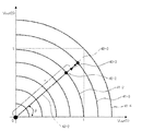
- the circumference shown in FIG. 3 represents a state in which the total output power for each band is maintained at a constant value while changing the output power ratio of each band.
- the intersection of the circumference 41-1 and the horizontal axis in FIG. 3 means that the load voltage Vout (2) of band 2 is not output.
- the intersection 42-1 between the circumference 41-1 and the straight line 43-1 when the angle ⁇ in FIG. 3 is 45 ° is the output power of the band 1 RF signal and the output of the band 2 RF signal. It means that the power matches (output power ratio is 0.5).
- the presence of a plurality of circumferences in FIG. 3 indicates that the total output power of each band takes a plurality of discrete values. That is, in FIG. 3, the longer the radius of each circumference, the greater the total output power of each band.
- the target value 40-1 is the total output power of the combined RF signals in band 1 and band 2 and the target value of the output power ratio of each band.
- a combination of load voltages (Vout (1)) that can be expressed by a circle 41-1 closest to the target point 40-1 and an intersection 42-1 that is an intersection of a straight line 43-1 connecting the origin and the target point 40-1.
- Vout (2) is output from the transmitter 10.
- the power amplifier 11-i when the sum of the output power of the band 1 RF signal 20-i and the output power of the band 2 RF signal 21-i reaches the saturation output power of the power amplifier 11-i, The power amplifier 11-i is saturated. That is, when the sum of the output power of each band reaches a certain value (saturated output power) specific to the power amplifier 11, the power amplifier 11 is saturated. Therefore, in each of the power amplifiers 11 to be operated, high power can be obtained by changing the power ratio of the RF signal for each band while maintaining the power sum of the RF signals of each band input to a constant value (saturated output power). The power amplifier can be operated in a saturated state where efficiency can be obtained, and the output power of each band can be continuously changed.
- the signal generation control unit 16 holds the total power of the input RF signal at a constant value (saturated output power) and transmits each band of the RF signal to be transmitted.
- the second control for changing the power ratio of the RF signal for each band is performed in each of the selected power amplifiers 11 according to the power ratio. For example, as described above, when the angle ⁇ shown in FIG. 3 is 45 °, the output power of the RF signal arranged in the band 1 is equal to the output power of the RF signal arranged in the band 2.
- the amplitude of the RF signal output to the power amplifier 11 is controlled. Note that such second control in the signal generation control unit 16 corresponds to setting the power of the RF signal of each band input to each power amplifier 11 according to the angle ⁇ , with reference to FIG. .
- the load impedance that can be seen from the output terminal of each power amplifier 11 changes depending on the on / off state of the other power amplifiers 11. Since the change in the load impedance may cause the power efficiency of each power amplifier 11 to deteriorate, the load impedance viewed from one of the power amplifiers 11 among the power amplifiers 11 is turned on by the other power amplifier 11. Even if / off is switched, it is desirable to change the power efficiency so as not to deteriorate. Therefore, the signal generation control unit 16 performs control so that the output power ratio of each band output by each power amplifier 11 is made uniform in each power amplifier 11. That is, the signal generation control unit 16 outputs the RF signal for each band so that the power ratio of the RF signal for each band output from each of the selected power amplifiers 11 is the same in each power amplifier 11. Control to change the power ratio.
- the transmission device 10 selects the power amplifier 11 to be operated from the plurality of power amplifiers 11, thereby combining the load voltages (Vout (1) and Vout (2)) output from the transmission device 10.
- the circumference where the intersection 42-1 exists is switched.
- the magnitude of the total output power of the RF signal to be transmitted is controlled (the first control is performed).
- the output power ratio of the RF signal for each band is controlled by continuously changing the output power ratio of the RF signal for each band while maintaining the saturation state of each power amplifier 11 (second control is performed). carry out).
- the operation of the signal generation control unit 16 described with reference to FIG. 3 selects the power amplifier 11 to be operated from the plurality of power amplifiers 11 based on the radius r, and the RF in each band based on the angle ⁇ . It can be explained that the output power ratio of the signal is continuously changed.
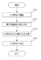
- the transmission apparatus 10 executes a transmission method of amplifying an RF signal by a plurality of power amplifiers 11 and transmitting the RF signal.
- the transmitting apparatus 10 amplifies RF signals arranged in at least two or more bands in the plurality of power amplifiers 11 (step S101).
- the transmission device 10 executes first control for selecting the power amplifier 11 that performs an amplification operation from among the plurality of power amplifiers 11 in accordance with the total power of the RF signals to be transmitted (step S102). After that, the transmission device 10 maintains the total power of the input RF signal constant in each of the selected power amplifiers 11 according to the power ratio of the RF signal to be transmitted for each band, and the RF signal for each band.
- Second control for changing the power ratio is executed (step S103). Thereafter, the transmission device 10 combines the RF signal output from the selected power amplifier 11 using the transformer element 13 (step S104).
- the transmission method according to the flowchart shown in FIG. 4 is an example, and is not intended to limit the order of processing to be executed.
- the order of the first control (step S102) and the second control (step S103) may be switched.
- step S101 may be executed after step S103.
- FIG. 5 is a diagram illustrating an example of a voltage amplitude waveform of band 1 (carrier frequency f1) output to the load 15 of the transmission apparatus 10.
- the solid line in FIG. 5 indicates the voltage amplitude waveform of the transmission apparatus 10, and the broken line indicates a voltage amplitude waveform (target waveform) without error. Since the transmitter 10 performs the two-dimensional quantization (output is limited on a discrete circumference) shown in FIG. 3, the output waveform shown in FIG. 5 is quantized with respect to the target waveform. An error has occurred.
- a WCDMA-DL Wideband Code Division Multiple Access-Down Link
- the result of FIG. 5 is acquired under the following conditions.
- the device size of each power amplifier 11 is a ratio of 2 0 : 2 1 :...: 2 N ⁇ 1 .
- the voltage amplitude output to the secondary side of the transformer element 13 during operation of the power amplifier 11 is a ratio of 2 0 : 2 1 :...: 2 N ⁇ 1 .
- Control of transmission power by turning on / off the power amplifier 11 is performed using a binary code.
- the sampling rate for controlling on / off of the power amplifier 11 is 30.72 MHz.
- the transmission apparatus 10 can obtain a voltage waveform close to a desired amplitude.
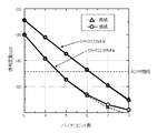
- FIG. 6 is a diagram showing the number n of power amplifiers 11 to be operated and the amount of signal distortion (ACPR: Adjacent Channel Power Ratio) output to the load 15 when a WCDMA-DL signal is transmitted in band 1. It is.
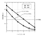
- FIG. 7 is a diagram illustrating the number n of power amplifiers 11 to be operated and the amount of signal distortion (ACPR) of band 2 output to the load 15 when a WCDMA-DL signal is transmitted in band 2. Note that the number n of the power amplifiers 11 matches the number of bits of the binary code used by the signal generation control unit 16.
- each power amplifier 11 is a ratio of 2 0 : 2 1 :...: 2 N ⁇ 1 .
- the voltage amplitude output to the secondary side of the transformer element 13 during operation of the power amplifier 11 is a ratio of 2 0 : 2 1 :...: 2 N ⁇ 1 .
- Control of transmission power by turning on / off the power amplifier 11 is performed using a binary code.
- the sampling rate (SR: Sampling Rate) when controlling on / off of the power amplifier 11 is two types of 30.72 MHz and 122.88 MHz.
- the signal distortion amount is calculated using a high band (dotted line in FIGS. 6 and 7) and a low band (circled solid line in FIGS. 6 and 7).
- the transmission apparatus 10 has substantially the same amount of signal distortion in the two bands.
- Comparative example Next, a comparative example compared with the transmission device 10 according to the first embodiment will be described.
- FIG. 8 is a diagram illustrating an example of a circuit configuration of the transmission apparatus 200 that digitally controls the transmission power of the power amplifier.
- the difference between the transmission apparatus 10 and the transmission apparatus 200 shown in FIG. 2 is that the signal generation control unit 17 does not support multiband communication.
- the transmission device 200 controls the output power to the load 15 by selecting the power amplifier 11 to be operated from the plurality of power amplifiers 11.
- the output power Pout output to the load 15 is given by the following equation (1).
- Pout ⁇ 1Psat (1) +... + ⁇ NPsat (n)
- Psat (i) is a saturation output of the power amplifier 11-i.
- (I) 0 ”is set.
- the signal generation control unit 17 of the transmission apparatus 200 determines the setting of the coefficient ⁇ (i) so that the output power Pout shown in Expression (1) becomes a desired value (approaching the desired value). In other words, the signal generation control unit 17 controls on / off of the power amplifier 11 so that the output power Pout becomes a desired value.
- the signal generation control unit 17 outputs an RF signal having an amplitude for causing each of the plurality of power amplifiers 11 to perform a saturation operation, and outputs the RF signal to each power amplifier 11.
- the power amplifier 11 may be controlled by output / non-output of the RF signal from the signal generation control unit 17 instead of the control for turning on / off the plurality of switches 12.
- each power amplifier 11 is always operated with a saturated output capable of obtaining high power efficiency, or is controlled in an off state in which no power consumption occurs, so that power saving can be realized.
- the load impedance that can be seen from the output terminal of each power amplifier 11 changes depending on on / off of the other power amplifiers 11.
- the output of each power amplifier 11 is combined in series using the transformer element 13 as in the transmission device 200 shown in FIG. 8, the load impedance seen from one of the plurality of power amplifiers 11 Even if ON / OFF is switched, the power efficiency changes so as not to deteriorate. Therefore, the transmission apparatus 200 illustrated in FIG. 8 is advantageous from the viewpoint of power consumption.
- the output power Pout is a discrete value generated from the plurality of power amplifiers 11. Therefore, a quantization error occurs between the desired output power value and the actual output power Pout.
- FIG. 9 is a diagram illustrating an example of a voltage amplitude waveform output to the load 15 of the transmission device 200.
- a voltage amplitude waveform (target waveform) without error is shown.
- the voltage amplitude waveform of the transmission apparatus 200 can take only a discrete constant value, a quantization error occurs with respect to the target waveform.
- the conditions for acquiring the voltage amplitude waveform shown in FIG. 9 are the same as the conditions for acquiring the voltage amplitude waveform shown in FIG.
- a method of increasing the number of power amplifiers can be considered as a method of reducing the influence of quantization error.
- the dynamic range of the output signal is expanded and the influence of quantization error can be reduced.
- FIG. 10 is a diagram showing the number n of power amplifiers 11 to be operated and the amount of signal distortion (ACPR) of the signal output to the load 15 when a WCDMA-DL signal is transmitted. Note that the conditions for acquiring the signal distortion amounts shown in FIG. 10 are the same as the conditions for acquiring the signal distortion amounts shown in FIGS. Referring to FIG. 10, it can be seen that the signal distortion amount (ACPR) is reduced by increasing the number of power amplifiers 11 (number of binary bits).
- the amount of signal distortion can also be reduced by increasing the sampling rate for controlling on / off of the power amplifier 11.
- the sampling rate for controlling on / off of the power amplifier 11 is 30.72 MHz
- the power distortion can be reduced to satisfy the standard amount of signal distortion (ACPR ⁇ 44.2 dBc) of WCDMA-DL.
- the number of amplifiers 11 (the number of binary bits) needs to be 7 or more.
- the sampling rate is set to 122.88 MHz, it is understood that the number of power amplifiers 11 may be five or more in order to satisfy the standard amount of signal distortion of WCDMA-DL.
- Non-Patent Document 2 the transmission device disclosed in Non-Patent Document 2 will be outlined.
- FIG. 11 is a diagram illustrating an example of a circuit configuration of a transmission device 200a that digitally controls the transmission power of the power amplifier.
- the difference between the transmission device 200 and the transmission device 200a is that the outputs of the power amplifier 11 are combined using ⁇ / 4 lines 18-1 to 18-n instead of the transformer elements 13-1 to 13-n. is there.
- the outputs of the plurality of power amplifiers 11 are serially combined by the transformer element 13, but in the transmission device 200a, the outputs of the plurality of power amplifiers 11 are combined in parallel by the ⁇ / 4 line 18. Excluding this difference, the transmission device 200 and the transmission device 200a perform the same operation.
- the load impedance seen from one of the power amplifiers 11 is degraded in power efficiency even when the other power amplifiers 11 are switched on / off. It changes so as not to.
- the transmission apparatus illustrated in FIG. 20 uses the two transmission apparatuses 200 to realize multiband communication.
- Transmitting apparatus 200-1 transmits RF signal 34 of band 1 (carrier frequency f1).
- Transmitting apparatus 200-2 transmits RF signal 35 of band 2 (carrier frequency f2).
- FIG. 20 by installing two transmission devices 200-1 and 200-2, it is possible to cope with dual band (two-band transmission).
- the combination of the load voltages (Vout (1), Vout (2)) is selected as shown in FIG. 21 by selecting the power amplifier 11 to be operated from among the power amplifiers 11. Among the indicated discrete points, the one closest to the target point is selected and output.
- a combination of load voltages (Vout (1), Vout (2)) represented by a discrete point 42-2 which is a discrete point closest to the target point 40-2 is the transmission device 200-1 and 200-2.
- all the power amplifiers 11 included in the transmission apparatus 200-1 that transmits the band 1 signal are turned on. It becomes a state.
- Vout (2) is lower than the maximum amplitude by one quantization interval, and thus the power amplifier of transmitting apparatus 200-2 that transmits a band 2 signal 11, only the power amplifier 11 responsible for the LSB is turned off, and the other power amplifiers 11 are turned on.
- multiband communication can be realized by using the transmission device 200 a instead of the transmission device 200.
- multiband communication can be realized using the two transmission devices 200.
- FIG. 5 showing the voltage amplitude waveform of the transmission apparatus 10
- FIG. 9 showing the voltage amplitude waveform of the transmission apparatus 200
- Multiband communication using two transmission devices 200 has a problem that the number of devices and output combining elements (for example, transformer elements 13) increases in proportion to the number of bands.
- the number of output combining elements for example, transformer elements 13
- the number of output combining elements does not increase.
- FIGS. 6 and 7 show that in the transmission apparatus 10, if the sampling rate of the power amplifier 11 is 122.88 MHz, the standard amount of signal distortion of WCDMA-DL (ACPR ⁇ 44) in both band 1 and band 2. .2 dBc) indicates that the number n of the power amplifiers 11 required to satisfy 5 is required. That is, FIG. 6 and FIG. 7 show that if one transmission device 10 including five power amplifiers 11 is used, multiband communication using two bands is possible.
- FIG. 10 showing characteristics relating to the signal distortion amount of the transmission apparatus 200 shows the standard amount of signal distortion of WCDMA-DL in one band (ACPR ⁇ 44.2 dBc) when the sampling rate of the power amplifier 11 is 122.88 MHz.
- the quantization error is suppressed to a desired value or less to realize power saving, and a necessary power amplifier and output.
- the number of synthesis elements can be reduced. This is advantageous when an increase in the size of the device when the output combining element is mounted with discrete components can be suppressed. Further, when the output synthesis element is mounted on an IC, it is possible to suppress an increase in the area and cost of the IC when it is multibanded.
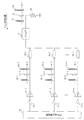
- FIG. 12 is a diagram illustrating an example of a circuit configuration of the transmission device 10a.
- the transmission device 10a supports transmission of a 3-band signal.
- the number of RF signals input to each power amplifier 11 is different between the transmission device 10 and the transmission device 10a.
- the transmission device 10a realizes multiband communication by inputting a 3-band RF signal to each power amplifier 11.
- the RF signals 20-i, 21-i, and 23-i output from the power amplifiers 11-i are combined for each carrier frequency in the transformer element 13, and are loaded via the filter 14 to the load 15 Is output.
- the transformer element usually has a wide band characteristic, and it is easy to synthesize a plurality of RF signals distributed over a wide frequency range. Also in the transmission apparatus 10a shown in FIG. 12, two output power controls, namely, discrete output power control by selecting the power amplifier 11 to be operated and continuous output power control by changing the output power ratio of each band. carry out. As a result, similarly to the transmission device 10, it is possible to suppress an increase in the number of transformer elements 13 when the multiband configuration is used.
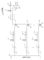
- FIG. 13 is a diagram illustrating an example of a circuit configuration of the transmission device 10b.
- a ⁇ / 4 line 18 is used instead of the transformer element 13. That is, the transmission device 10b includes a combining unit including the same number of transmission line elements ( ⁇ / 4 lines) as the plurality of power amplifiers 11. One end of the ⁇ / 4 line 18 is connected to the corresponding power amplifier 11, and the other end of the plurality of ⁇ / 4 lines 18 is connected in parallel.
- the ⁇ / 4 line 18 included in the transmission device 10b needs to correspond to a plurality of bands to be transmitted.
- the band of the ⁇ / 4 line is usually narrow. Making the ⁇ / 4 line 18 correspond to a plurality of bands can be realized by the following description.
- Non-Patent Document 3 discloses a ⁇ / 4 line that can be used as an output combining element.
- Non-Patent Document 3 discloses that a circuit corresponding to a ⁇ / 4 line 18 corresponding to two bands includes a transmission line 301 having a characteristic impedance Z1 and an electric length ⁇ 1, and transmission lines 302 and 303 having a characteristic impedance Z2 and an electric length ⁇ 2. It is disclosed that it can be configured by (see FIG. 14).
- a circuit corresponding to the ⁇ / 4 line 18 corresponding to two bands is constituted by transmission lines 304 and 305 having a characteristic impedance Z1 and an electric length ⁇ 1, and a transmission line 306 having a characteristic impedance Z2 and an electric length ⁇ 2.
- the ⁇ / 4 line 18 for three or more bands can be realized by connecting a plurality of circuits shown in FIG. 14 or 15 in series and increasing the number of design parameters (characteristic impedance and electrical length).
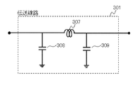
- the transmission lines 301 to 306 can be composed of lumped constant elements shown in FIG. That is, the transmission lines 301 to 306 can be configured by lumped constant elements using the inductance element 307 and the capacitive elements 308 and 309 as in the circuit configuration shown in FIG. Also in the transmission device 10b shown in FIG. 13, two output power controls, namely, discrete output power control by selecting the power amplifier 11 to be operated and continuous output power control by changing the output power ratio of each band. carry out. As a result, similarly to the transmission device 10, it is possible to suppress an increase in the number of ⁇ / 4 lines 18 when multibanding is performed.
- FIG. 17 is a diagram illustrating an example of a circuit configuration of the transmission device 40 according to the second embodiment.
- the difference between the transmission device 10 and the transmission device 40 according to the first embodiment is that the control of the signal generation control unit 19 is different from the signal generation control unit 16.
- the transmission device 40 causes the power amplifier 11-1 to perform an analog operation.
- the power amplifiers 11-2 to 11n other than the power amplifier 11-1 operate in a saturated state or perform an on / off operation (digital control) in which the operation state is turned off.
- the transmission device 40 The operation of the transmission device 40 will be described with reference to FIG.
- the combined outputs of the power amplifiers 11-2 to 11-n that perform the on / off operation (digital operation) take values on the circumference shown in FIG. 18 depending on the selection of the power amplifier to be operated.
- a desired output voltage is expressed as a target point 40-3.
- a circle 41-2 having a radius shorter than the position of the target point 40-3 and closest to the target point 40-3, a straight line 43-2 connecting the target point 40-3 and the origin, and a circle 41-2. Let the intersection point be 42-2. At this time, on / off of the power amplifiers 11-2 to 11-n is controlled so that the combined output of the power amplifiers 11-2 to 11-n becomes the intersection point 42-2.
- the signal generation control unit 19 performs control so that the output power of the power amplifier 11-1 performing the analog operation becomes an output voltage corresponding to the difference between the target point 40-3 and the intersection 42-2.
- the signal generation control unit 19 uses the power amplifier so that the power of the RF signal after signal amplification in the power amplifier 11-1 corresponds to the power difference between the target point 40-3 and the intersection 42-2.
- the amplitude of the RF signal supplied to 11-1 is controlled.
- a radius 41-3 that is longer than the position of the target point 40-3 and closest to the target point 40-3, a straight line 43-2 that connects the target point 40-3 and the origin, and a circumference 41- The intersection of 3 is defined as an intersection 42-3.
- the signal generation control unit 19 can set the range of the output voltage of the transmission device 40 between the intersection point 42-2 and the intersection point 42-3 by controlling the power amplifier 11-1 that performs the analog operation.
- the signal generation control unit 19 performs analog control on the amplitude of the RF signal output to the power amplifier 11-1, thereby increasing the power consumption of the power amplifier 11-1.
- the transmission device 40 has a substantial error. A signal corresponding to the target point 40-3 not to be output can be output.
- the same number of transmission devices 200 as the number of bands to be supported are prepared to realize multiband communication, and the case where multiband communication is realized by one transmission device 10. Then, the quantization error (that is, the difference between the combined output and the target point) is almost the same. Therefore, the power consumption is almost the same when the power amplifier 11-1 is operated in an analog manner in the transmission device 200 and when the power amplifier 11-1 is operated in an analog manner in the transmission device 40.
- the transmission apparatus 200 increases the number of output combining elements (for example, transformer elements) in proportion to the number of bands, whereas the transmission apparatus 40 outputs even if the number of bands increases.
- the number of synthesis elements does not increase. That is, the transmitter 40 is more advantageous in terms of the trade-off relationship between the number (n ⁇ 1) of the power amplifiers 11 that perform the on / off operation and the power consumption of the power amplifier that performs the analog operation. Furthermore, the superiority of the transmitter 40 increases as the number of corresponding bands increases.
- the error can be reduced by analog control of the power amplifier 11-1.
- the transmission device 40 has a predetermined power amplifier (for example, the power amplifier 11-1) among the plurality of power amplifiers 11 according to the total power of the RF signals to be transmitted.
- the total power of the RF signal input to is changed as a continuous value, and the other power amplifiers 11-2 to 11-n are operated in saturation.
- the transmission device 40 can output a signal that is substantially free of quantization error.
- the transmitter 40a is implemented by mounting the power amplifiers 11-1 to 11-n included in the transmitter 40 as analog amplifiers that perform analog operations. Further, the power amplifiers to be operated are selected from the power amplifiers 11-1 to 11-n by the switches 12-1 to 12-n.
- the k + 1 power amplifiers 11 reduce the output power from the saturated output at the same ratio (backoff is performed).
- the output amplitude of the RF signal is set so as to output a desired signal (target point 40-3).
- the transmitter 40a sets the output amplitude of the RF signal so as to output a desired signal (target point 40-3).
- the number of output combining elements does not increase even if the corresponding number of bands increases.
- FIG. 19 is a diagram illustrating an example of a circuit configuration of the transmission device 40b.
- the difference between the transmission device 40 and the transmission device 40b shown in FIG. 17 is that a power control unit 50 is connected to the power amplifier 11-1.
- the power supply control unit 50 controls the power supply voltage of the power amplifier 11-1.
- the power supply controller 50 changes the power supply voltage of the power amplifier 11-1 in which the total power of the input RF signal is changed as a continuous value.
- the power amplifier 11-1 performs a saturation operation.
- the saturation output of the power amplifier 11-1 (the total power of the RF signal 20-1 and the RF signal 21-1) is continuously (analog-like) in proportion to the square of the power supply voltage of the power amplifier 11-1. ) Can be changed. That is, in the transmission device 40 according to the second embodiment, the amplitude of the output signal of the power amplifier 11-1 is controlled by the amplitude of the RF signal input to the power amplifier 11-1, whereas the transmission device 40b The amplitude of the output signal of the power amplifier 11-1 is controlled by changing the power supply voltage of the amplifier 11-1.
- a ⁇ / 4 line can be used as the output combining element shown in FIG. 19 instead of the transformer element 13.
- the power amplifier 11-1 since the power amplifier 11-1 itself performs a saturation operation, the power consumption of the power amplifier 11-1 performing an analog operation can be suppressed to a low level.
- the number of output combining elements does not increase even if the corresponding number of bands increases.
- [Appendix 1] This is the same as the transmission apparatus according to the first aspect described above.
- [Appendix 2] The transmission apparatus according to supplementary note 1, wherein the second control unit changes a power ratio of an RF signal for each band in each of the selected amplification units so that each of the selected amplification units performs a saturation operation.
- [Appendix 3] The second control unit changes, as a continuous value, the total power of the RF signal input to a predetermined amplification unit among the plurality of amplification units according to the total power of the RF signal to be transmitted.
- the transmitter according to appendix 1 or 2 wherein the amplifying unit is operated in saturation.
- the transmission apparatus according to appendix 3, further comprising a power supply control unit that changes a power supply voltage of the predetermined amplification unit.
- the second control unit changes the power ratio of the RF signal for each band so that the power ratio of the RF signal for each band output from each of the selected amplifiers is the same in each amplifier.
- the transmitting device according to any one of appendices 1 to 4.
- the combining unit is configured by the same number of transformer elements as the plurality of amplifiers, and the primary side of the transformer elements and the corresponding amplifier are connected, The transmission device according to any one of appendices 1 to 5, wherein secondary sides of the plurality of transformer elements are connected in series.
- the combining unit includes the same number of transmission line elements as the plurality of amplifiers, and one end of the transmission line element is connected to the corresponding amplifier, and the other end of the plurality of transmission line elements is in parallel.
- the transmitting device according to any one of appendices 1 to 5, which is connected.
- [Appendix 8] The transmission device according to appendix 7, wherein the transmission line element includes a lumped constant element.
- [Appendix 9] This is the same as the transmission method according to the second viewpoint described above.
- Appendix 10 The transmission method according to appendix 9, wherein in the second control step, the power ratio of the RF signal for each band is changed in each of the selected amplifiers so that each of the selected amplifiers performs a saturation operation. .
Landscapes
- Engineering & Computer Science (AREA)
- Power Engineering (AREA)
- Computer Networks & Wireless Communication (AREA)
- Signal Processing (AREA)
- Amplifiers (AREA)
- Transmitters (AREA)
Abstract
Description
本発明は、日本国特許出願:特願2013-103931号(2013年05月16日出願)の優先権主張に基づくものであり、同出願の全記載内容は引用をもって本書に組み込み記載されているものとする。
本発明は、送信装置及び送信方法に関する。特に、無線通信で使用され、複数のバンドに配置されたRF(Radio Frequency)信号を送信する送信装置及び送信方法に関する。
なお、本方法は、RF信号を増幅する増幅部という特定の機械に結びつけられている。
第1の実施形態について、図面を用いてより詳細に説明する。
・各電力増幅器11のデバイスサイズは、20:21:・・・:2N-1の比率とする。
・電力増幅器11の動作時にトランス素子13の2次側に出力される電圧振幅は、20:21:・・・:2N-1の比率とする。
・電力増幅器11のオン/オフによる送信電力の制御を、バイナリコードを用いて行う。
・電力増幅器11のオン/オフを制御する際のサンプリングレートは、30.72MHzとする。
なお、電力増幅器11及びトランス素子13の個数nは、送信装置10の制御に用いられるバイナリコードのビット数(桁数)に等しく、図3においては「n=3」とする。
・各電力増幅器11のデバイスサイズは、20:21:・・・:2N-1の比率とする。
・電力増幅器11の動作時にトランス素子13の2次側に出力される電圧振幅は、20:21:・・・:2N-1の比率とする。
・電力増幅器11のオン/オフによる送信電力の制御を、バイナリコードを用いて行う。
・電力増幅器11のオン/オフを制御する際のサンプリングレート(SR;Sampling Rate)は、30.72MHz、122.88MHzの2種とする。
・信号歪量の算出は、高域側のバンド(図6及び図7の三角付の点線)と低域側のバンド(図6及び図7の丸付の実線)にて行う。
[比較例]
次に、第1の実施形態に係る送信装置10と比較する比較例について説明する。
Pout=α1Psat(1)+・・・+αNPsat(n) ・・・(1)
なお、Psat(i)は電力増幅器11-iの飽和出力である。また、係数α(i)は、電力増幅器11-iを動作させる場合に「α(i)=1」と設定され、電力増幅器11-iをオフにして電力を非出力とさせる場合に「α(i)=0」と設定される。
図12は、送信装置10aの回路構成の一例を示す図である。送信装置10aは、3バンドの信号の送信に対応している。送信装置10と送信装置10aでは、各電力増幅器11に入力するRF信号の数が相違する。
図13は、送信装置10bの回路構成の一例を示す図である。送信装置10と送信装置10bでは、トランス素子13に代えて、λ/4線路18を使用する。つまり、送信装置10bは、複数の電力増幅器11と同数の伝送線路素子(λ/4線路)からなる合成部を備える。λ/4線路18の一端は、対応する電力増幅器11に接続されると共に、複数のλ/4線路18の他の一端は並列に接続される。
続いて、第2の実施形態について図面を参照して詳細に説明する。
送信装置40に含まれる電力増幅器11-1~11-nを、アナログ動作を行うアナログアンプとして実装するのが、送信装置40aである。また、スイッチ12-1~12-nにより、電力増幅器11-1~11-nのなかで動作させる電力増幅器が選択される。
図19は、送信装置40bの回路構成の一例を示す図である。図17に示す送信装置40と送信装置40bの相違点は、電力増幅器11-1に電源制御部50が接続されている点である。電源制御部50は、電力増幅器11-1の電源電圧を制御する。電源制御部50は、入力されるRF信号の電力総和が連続値として変更される電力増幅器11-1の電源電圧を変更する。
上述の第1の視点に係る送信装置のとおりである。
[付記2]
前記第2の制御部は、前記選択された増幅部のそれぞれが飽和動作を行うように、前記選択された増幅部のそれぞれにおいて、バンドごとのRF信号の電力比を変更する付記1の送信装置。
[付記3]
前記第2の制御部は、送信するRF信号の電力総和に応じて、前記複数の増幅部のうち、予め定めた増幅部に入力されるRF信号の電力総和を連続値として変更し、他の増幅部を飽和動作させる付記1又は2の送信装置。
[付記4]
前記予め定めた増幅部の電源電圧を変更する電源制御部をさらに備える付記3の送信装置。
[付記5]
前記第2の制御部は、前記選択された増幅器のそれぞれから出力される、バンドごとのRF信号の電力比が、それぞれの増幅器において同一となるように、バンドごとのRF信号の電力比を変更する付記1乃至4のいずれか一に記載の送信装置。
[付記6]
前記合成部は、前記複数の増幅器と同数のトランス素子により構成され、前記トランス素子の1次側と、対応する前記増幅器と、が接続されると共に、
前記複数のトランス素子の2次側は直列に接続される、付記1乃至5のいずれか一に記載の送信装置。
[付記7]
前記合成部は、前記複数の増幅器と同数の伝送線路素子により構成され、前記伝送線路素子の一端は、対応する前記増幅器に接続されると共に、前記複数の伝送線路素子の他の一端は並列に接続される、付記1乃至5のいずれか一に記載の送信装置。
[付記8]
前記伝送線路素子は、集中定数素子から構成される付記7の送信装置。
[付記9]
上述の第2の視点に係る送信方法のとおりである。
[付記10]
前記第2の制御工程は、前記選択された増幅部のそれぞれが飽和動作を行うように、前記選択された増幅部のそれぞれにおいて、バンドごとのRF信号の電力比を変更する付記9の送信方法。
[付記11]
前記第2の制御工程は、送信するRF信号の電力総和に応じて、前記複数の増幅部のうち、予め定めた増幅部に入力されるRF信号の電力総和を連続値として変更し、他の増幅部を飽和動作させる付記9又は10の送信方法。
[付記12]
前記予め定めた増幅部の電源電圧を変更する工程をさらに含む付記11の送信方法。
11、11-1~11-n 電力増幅器(PA;Power Amp)
12、12-1~12-n スイッチ
13、13-1~13-n トランス素子
14 フィルタ
15 負荷
16、17、19 信号発生制御部
18、18-1~18-n λ/4線路
20-1~20-n、21-1~21-n、22-1~22-n、23-1~23-n RF信号
31~35 合成RF信号
40-1~40-3 目標点
41-1~41-4 円周
42-1、42-3 交点
42-2 離散点
43-1、43-2 直線
50 電源制御部
101 増幅部
102 第1の制御部
103 第2の制御部
104 合成部
301~306 伝送線路
307 インダクタンス素子
308、309 容量素子
Claims (10)
- 少なくとも2以上のバンドに配置されたRF信号を増幅する、複数の増幅部と、
送信するRF信号の電力総和に応じて、前記複数の増幅部のうち、増幅動作を行う増幅部を選択する第1の制御部と、
送信するRF信号のバンドごとの電力比に応じて、前記選択された増幅部のそれぞれにおいて、入力するRF信号の電力総和を一定に保持しつつ、バンドごとのRF信号の電力比を変更する第2の制御部と、
前記選択された増幅部が出力するRF信号を合成する合成部と、
を備える送信装置。 - 前記第2の制御部は、前記選択された増幅部のそれぞれが飽和動作を行うように、前記選択された増幅部のそれぞれにおいて、バンドごとのRF信号の電力比を変更する請求項1の送信装置。
- 前記第2の制御部は、送信するRF信号の電力総和に応じて、前記複数の増幅部のうち、予め定めた増幅部に入力されるRF信号の電力総和を連続値として変更し、他の増幅部を飽和動作させる請求項1又は2の送信装置。
- 前記予め定めた増幅部の電源電圧を変更する電源制御部をさらに備える請求項3の送信装置。
- 前記第2の制御部は、前記選択された増幅器のそれぞれから出力される、バンドごとのRF信号の電力比が、それぞれの増幅器において同一となるように、バンドごとのRF信号の電力比を変更する請求項1乃至4のいずれか一項に記載の送信装置。
- 前記合成部は、前記複数の増幅器と同数のトランス素子により構成され、前記トランス素子の1次側と、対応する前記増幅器と、が接続されると共に、
前記複数のトランス素子の2次側は直列に接続される、請求項1乃至5のいずれか一項に記載の送信装置。 - 前記合成部は、前記複数の増幅器と同数の伝送線路素子により構成され、前記伝送線路素子の一端は、対応する前記増幅器に接続されると共に、前記複数の伝送線路素子の他の一端は並列に接続される、請求項1乃至5のいずれか一項に記載の送信装置。
- 前記伝送線路素子は、集中定数素子から構成される請求項7の送信装置。
- 複数の増幅部によりRF信号を増幅して、RF信号を送信する送信方法であって、
複数の増幅部において、少なくとも2以上のバンドに配置されたRF信号を増幅する増幅工程と、
送信するRF信号の電力総和に応じて、前記複数の増幅部のうち、増幅動作を行う増幅部を選択する第1の制御工程と、
送信するRF信号のバンドごとの電力比に応じて、前記選択された増幅部のそれぞれにおいて、入力するRF信号の電力総和を一定に保持しつつ、バンドごとのRF信号の電力比を変更する第2の制御工程と、
前記選択された増幅部が出力するRF信号を合成する合成工程と、
を含む送信方法。 - 前記第2の制御工程は、前記選択された増幅部のそれぞれが飽和動作を行うように、前記選択された増幅部のそれぞれにおいて、バンドごとのRF信号の電力比を変更する請求項9の送信方法。
Priority Applications (2)
| Application Number | Priority Date | Filing Date | Title |
|---|---|---|---|
| US14/888,472 US9847761B2 (en) | 2013-05-16 | 2014-05-14 | Transmission apparatus and transmission method |
| JP2015517112A JP6458729B2 (ja) | 2013-05-16 | 2014-05-14 | 送信装置及び送信方法 |
Applications Claiming Priority (2)
| Application Number | Priority Date | Filing Date | Title |
|---|---|---|---|
| JP2013-103931 | 2013-05-16 | ||
| JP2013103931 | 2013-05-16 |
Publications (1)
| Publication Number | Publication Date |
|---|---|
| WO2014185459A1 true WO2014185459A1 (ja) | 2014-11-20 |
Family
ID=51898435
Family Applications (1)
| Application Number | Title | Priority Date | Filing Date |
|---|---|---|---|
| PCT/JP2014/062865 Ceased WO2014185459A1 (ja) | 2013-05-16 | 2014-05-14 | 送信装置及び送信方法 |
Country Status (3)
| Country | Link |
|---|---|
| US (1) | US9847761B2 (ja) |
| JP (1) | JP6458729B2 (ja) |
| WO (1) | WO2014185459A1 (ja) |
Families Citing this family (4)
| Publication number | Priority date | Publication date | Assignee | Title |
|---|---|---|---|---|
| EP3272026B1 (en) * | 2015-03-20 | 2020-04-29 | Andrew Wireless Systems GmbH | Module for combining signals having different frequencies |
| US10027354B2 (en) * | 2015-03-25 | 2018-07-17 | Intel IP Corporation | Phased array weighting for power efficiency improvement with high peak-to-average power ratio signals |
| US10361661B2 (en) * | 2015-09-01 | 2019-07-23 | Nec Corporation | Power amplification apparatus and television signal transmission system |
| US10211904B2 (en) * | 2016-04-19 | 2019-02-19 | Telefonaktiebolaget Lm Ericsson (Publ) | Power control and beamforming with a plurality of power amplifiers |
Citations (3)
| Publication number | Priority date | Publication date | Assignee | Title |
|---|---|---|---|---|
| JP2005223827A (ja) * | 2004-02-09 | 2005-08-18 | Nec Saitama Ltd | 高周波合成回路及び送信装置 |
| JP2006222828A (ja) * | 2005-02-14 | 2006-08-24 | Hitachi Kokusai Electric Inc | 増幅装置 |
| JP2010028632A (ja) * | 2008-07-23 | 2010-02-04 | Hitachi Kokusai Electric Inc | 増幅器 |
Family Cites Families (17)
| Publication number | Priority date | Publication date | Assignee | Title |
|---|---|---|---|---|
| US4439740A (en) * | 1982-04-01 | 1984-03-27 | Rockwell International Corporation | Corporate amplifier apparatus with improved degradation |
| JPH04321305A (ja) | 1991-04-20 | 1992-11-11 | Nec Corp | 振幅変調送信機 |
| JP2610729B2 (ja) | 1991-08-29 | 1997-05-14 | 日本放送協会 | 振幅変調方式 |
| US5304943A (en) * | 1992-11-16 | 1994-04-19 | Harris Corporation | In-phase combiner and RF recovery system |
| US5781066A (en) * | 1996-03-11 | 1998-07-14 | The Mitre Corporation | Pulse waveform generator |
| US5886573A (en) * | 1998-03-06 | 1999-03-23 | Fujant, Inc. | Amplification using amplitude reconstruction of amplitude and/or angle modulated carrier |
| US6118343A (en) * | 1999-05-10 | 2000-09-12 | Tyco Electronics Logistics Ag | Power Amplifier incorporating single drain switch and single negative voltage generator |
| JP2006013753A (ja) * | 2004-06-24 | 2006-01-12 | Renesas Technology Corp | 無線通信システムおよび半導体集積回路 |
| JP2007019578A (ja) * | 2005-07-05 | 2007-01-25 | Hitachi Ltd | 電力増幅器およびそれを用いた送信機 |
| JP2008048321A (ja) * | 2006-08-21 | 2008-02-28 | Nec Corp | 無線送信装置及びその送信電力レベル調整システム |
| JP2009010484A (ja) * | 2007-06-26 | 2009-01-15 | Mitsubishi Electric Corp | マルチバンド増幅器 |
| US8315578B2 (en) * | 2008-07-15 | 2012-11-20 | Research In Motion Limited | Mobile wireless communications device with separate in-phase and quadrature power amplification |
| WO2010079631A1 (ja) * | 2009-01-09 | 2010-07-15 | 三菱電機株式会社 | マルチポートアンプおよびそれを用いた無線装置 |
| US8537153B2 (en) * | 2009-12-30 | 2013-09-17 | Himax Technologies Limited | Source driver having multiplexers positioned between differential amplifiers and buffers and associated driving method |
| WO2013027538A1 (ja) * | 2011-08-23 | 2013-02-28 | 日本電気株式会社 | 送信機 |
| US8829993B2 (en) * | 2012-10-30 | 2014-09-09 | Eta Devices, Inc. | Linearization circuits and methods for multilevel power amplifier systems |
| US8824978B2 (en) * | 2012-10-30 | 2014-09-02 | Eta Devices, Inc. | RF amplifier architecture and related techniques |
-
2014
- 2014-05-14 WO PCT/JP2014/062865 patent/WO2014185459A1/ja not_active Ceased
- 2014-05-14 JP JP2015517112A patent/JP6458729B2/ja not_active Expired - Fee Related
- 2014-05-14 US US14/888,472 patent/US9847761B2/en active Active
Patent Citations (3)
| Publication number | Priority date | Publication date | Assignee | Title |
|---|---|---|---|---|
| JP2005223827A (ja) * | 2004-02-09 | 2005-08-18 | Nec Saitama Ltd | 高周波合成回路及び送信装置 |
| JP2006222828A (ja) * | 2005-02-14 | 2006-08-24 | Hitachi Kokusai Electric Inc | 増幅装置 |
| JP2010028632A (ja) * | 2008-07-23 | 2010-02-04 | Hitachi Kokusai Electric Inc | 増幅器 |
Also Published As
| Publication number | Publication date |
|---|---|
| US20160191003A1 (en) | 2016-06-30 |
| US9847761B2 (en) | 2017-12-19 |
| JP6458729B2 (ja) | 2019-01-30 |
| JPWO2014185459A1 (ja) | 2017-02-23 |
Similar Documents
| Publication | Publication Date | Title |
|---|---|---|
| US9450541B2 (en) | Systems and methods related to linear and efficient broadband power amplifiers | |
| US8471638B2 (en) | Doherty amplifier | |
| US8995936B2 (en) | Communication system with band, mode, impedance and linearization self-adjustment | |
| JP5722173B2 (ja) | デュアルバンド無線周波送信機 | |
| US8988147B2 (en) | Multi-way Doherty amplifier | |
| JP2016042695A (ja) | 信号合成器、電力増幅器モジュール、および無線装置 | |
| US10439560B2 (en) | Power amplification module | |
| US8718581B2 (en) | Method and apparatus for optimizing current consumption of amplifiers with power control | |
| US9231626B2 (en) | Wireless communication apparatus, Doherty amplifier, and method for controlling wireless communication | |
| US20150340996A1 (en) | Power amplifier, transceiver, and base station | |
| CN108111129B (zh) | 功率放大器 | |
| JP2010021719A (ja) | ドハティ増幅器 | |
| JP6458729B2 (ja) | 送信装置及び送信方法 | |
| CN104640011A (zh) | 一种应用于ap的双频功放装置及ap设备 | |
| JP5754362B2 (ja) | 増幅器 | |
| WO2015093021A1 (ja) | 送信装置および送信方法 | |
| JP2011155357A (ja) | マルチバンド電力増幅器 | |
| JP2016201787A (ja) | 電力増幅モジュール | |
| JP2011182312A (ja) | 増幅器 | |
| Esch | High-efficiency Doherty power amplifiers: Historical aspect and modern trends | |
| WO2016086975A1 (en) | An amplifying system for amplifying a communication signal | |
| JP5978693B2 (ja) | 増幅装置、無線通信装置、及び負荷変動器 | |
| CN107241073A (zh) | 一种提高线性度的并行结构功率放大器 | |
| JP2014116757A (ja) | 増幅回路及び通信装置 | |
| JP2013046384A (ja) | 増幅装置及び無線通信装置 |
Legal Events
| Date | Code | Title | Description |
|---|---|---|---|
| 121 | Ep: the epo has been informed by wipo that ep was designated in this application |
Ref document number: 14798412 Country of ref document: EP Kind code of ref document: A1 |
|
| WWE | Wipo information: entry into national phase |
Ref document number: 14888472 Country of ref document: US |
|
| ENP | Entry into the national phase |
Ref document number: 2015517112 Country of ref document: JP Kind code of ref document: A |
|
| NENP | Non-entry into the national phase |
Ref country code: DE |
|
| 122 | Ep: pct application non-entry in european phase |
Ref document number: 14798412 Country of ref document: EP Kind code of ref document: A1 |