WO2014185241A1 - 静電容量センサ - Google Patents
静電容量センサ Download PDFInfo
- Publication number
- WO2014185241A1 WO2014185241A1 PCT/JP2014/061480 JP2014061480W WO2014185241A1 WO 2014185241 A1 WO2014185241 A1 WO 2014185241A1 JP 2014061480 W JP2014061480 W JP 2014061480W WO 2014185241 A1 WO2014185241 A1 WO 2014185241A1
- Authority
- WO
- WIPO (PCT)
- Prior art keywords
- circuit
- oscillation
- capacitance
- frequency
- feedback
- Prior art date
- Legal status (The legal status is an assumption and is not a legal conclusion. Google has not performed a legal analysis and makes no representation as to the accuracy of the status listed.)
- Ceased
Links
Images



Classifications
-
- H—ELECTRICITY
- H03—ELECTRONIC CIRCUITRY
- H03K—PULSE TECHNIQUE
- H03K17/00—Electronic switching or gating, i.e. not by contact-making and –breaking
- H03K17/94—Electronic switching or gating, i.e. not by contact-making and –breaking characterised by the way in which the control signals are generated
- H03K17/945—Proximity switches
- H03K17/955—Proximity switches using a capacitive detector
-
- H—ELECTRICITY
- H03—ELECTRONIC CIRCUITRY
- H03K—PULSE TECHNIQUE
- H03K2217/00—Indexing scheme related to electronic switching or gating, i.e. not by contact-making or -breaking covered by H03K17/00
- H03K2217/94—Indexing scheme related to electronic switching or gating, i.e. not by contact-making or -breaking covered by H03K17/00 characterised by the way in which the control signal is generated
- H03K2217/96—Touch switches
- H03K2217/9607—Capacitive touch switches
- H03K2217/960735—Capacitive touch switches characterised by circuit details
Definitions
- the present invention relates to a capacitance of a detection electrode or a capacitance sensor that detects a change thereof, and more particularly to a capacitance sensor that uses an oscillation circuit.
- Patent Document 1 discloses a fluid that uses the above-described capacitive proximity sensor.
- a fluid detection sensor for detecting presence / absence, configuration, state change, and the like is disclosed.
- the capacitive proximity sensor includes an oscillation circuit as a circuit for detecting the change in capacitance, and a part of the oscillation circuit serves as a detection electrode.
- the capacitance C X of the detection electrode increases and the oscillation frequency f OSC changes.
- the capacitive proximity sensor includes a determination circuit that determines whether or not the oscillation frequency f OSC of the oscillation circuit has reached a predetermined reference value, and the proximity of the object is determined based on the determination result. Can be detected.
- FIG. 5 is a circuit diagram showing a schematic configuration of the capacitive proximity sensor.
- the capacitive proximity sensor 101 includes an oscillation circuit 111 and a determination circuit 112.
- the oscillation circuit 111 is a Wien bridge oscillation circuit including a detection electrode 113, an operational amplifier A, a capacitance element C 2 , and resistance elements R 1 to R 4 .
- the sign of the resistive element is also the resistance value of the resistive element
- the sign of the capacitive element is also the capacitance of the capacitive element.
- the oscillation circuit 111 outputs a signal having an oscillation frequency f OSC that satisfies the above formula (a) to the determination circuit 112.
- the oscillation circuit 113 oscillates under the condition that the feedback rate C 2 ⁇ R 2 / (C X ⁇ R 2 + C 2 ⁇ R 2 + C 2 ⁇ R 1 ) of positive feedback is negative at the oscillation frequency f OSC .
- the feedback rate R 4 / (R 3 + R 4 ) or higher which is expressed by the following formula. R 3 / R 4 ⁇ (C X / C 2 ) + (R 1 / R 2 ) (b).
- the determination circuit 112 monitors a change in the oscillation frequency f OSC of the signal from the oscillation circuit 111, converts it into a required signal according to the purpose, and outputs it.
- the determination circuit 112 includes a period / voltage conversion circuit that converts the oscillation frequency f OSC into a DC voltage, a comparator that compares the converted DC voltage with a predetermined reference value, and the DC voltage that is larger or smaller than the reference value. And an output circuit for issuing a predetermined alarm and a control signal.
- Japanese Patent Publication Japanese Patent Laid-Open No. 11-230815 (published Aug. 27, 1999)”
- the capacitance C X of the detection electrode 113 when there is a fluid or when there is no fluid is defined as a reference capacitance C X0
- the detected capacitance C X is What is necessary is just to examine how much it differs from the reference capacitance C X0 . That is, the oscillation frequency f OSC of the oscillator circuit 111 corresponding to the reference capacitance C X0 as the reference oscillation frequency f OSC 0, may be obtained a difference between the detected and the oscillation frequency f OSC reference oscillation frequency f OSC 0.
- the range of the capacitance C X to be detected may be the reference capacitance C X0 and the vicinity thereof, and the range of the detectable oscillation frequency f OSC . May be at or near the reference oscillation frequency f OSC0 .
- the conventional capacitive proximity sensor 101 As a capacitance sensor for detecting capacitance, it is necessary to expand the detection range of the capacitance CX .
- the following problems occur. That is, as the capacitance C X increases, the oscillation frequency f OSC of the oscillation circuit 113 decreases as shown in the above equation (a), and the amplification factor decreases as the feedback rate of the positive feedback decreases. Eventually, the above equation (b) is not satisfied and oscillation does not occur.
- the capacitance C X is decreased, the oscillation frequency f OSC of the oscillation circuit 113 is increased, and the amplification factor is increased by increasing the feedback factor of the positive feedback. As a result, the waveform of the sine wave is distorted. As a result, the above formula (a) is not satisfied.
- the present invention has been made in view of the above problems, and an object of the present invention is to provide a capacitance sensor in which the capacitance detection range is expanded as compared with the prior art.
- a capacitance sensor is a capacitance sensor that detects a capacitance of a detection electrode or a change thereof.
- an amplification circuit and a signal amplified by the amplification circuit Among them, an oscillation circuit that oscillates at an oscillation frequency included in the frequency band by providing a feedback circuit that feeds back a signal in a predetermined frequency band to the amplifier circuit at a predetermined feedback rate, the oscillation frequency and the An oscillation circuit in which the detection electrode is connected to the feedback circuit and an amplitude of an oscillation signal that is an output signal of the oscillation circuit is less than or equal to a predetermined upper limit value so that a feedback rate depends on the capacitance of the detection electrode
- an amplitude control circuit for controlling a feedback rate of the feedback circuit is provided.
- the amplitude of the oscillation signal of the oscillation circuit increases due to a change in the capacitance of the detection electrode, the amplitude is maintained below a predetermined upper limit value.
- the amplitude is maintained below a predetermined upper limit value.
- FIGS. 1 to 4 Embodiments of the present invention will be described with reference to FIGS. 1 to 4 as follows.
- members having the same functions as those shown in the embodiments are denoted by the same reference numerals, and description thereof is omitted as appropriate.
- FIG. 1 is a block diagram showing a schematic configuration of the capacitance sensor according to the first embodiment of the present invention.
- the capacitance sensor 1 detects the capacitance C X of the detection electrode 2, and is used for, for example, a water level sensor, a touch sensor, a proximity sensor, and the like.
- the capacitance sensor 1 includes the detection electrode 2, an oscillation circuit 11, an evaluation circuit 12, an amplitude control circuit 13, and a frequency control circuit 14.
- the oscillation circuit 11 includes an operational amplifier OP1 and a feedback circuit 21 that feeds back a signal in a predetermined frequency band among signals amplified by the operational amplifier OP1 to the operational amplifier OP1 at a predetermined feedback rate. It oscillates at the oscillation frequency f OSC included in the band.
- the detection electrode 2 is connected to the feedback circuit 21 so that the oscillation frequency f OSC and the feedback rate depend on the capacitance C X of the detection electrode 2.
- the evaluation circuit 12 evaluates the capacitance C X of the detection electrode 2 based on the oscillation frequency f OSC of the oscillation circuit 11.
- the amplitude control circuit 13 controls the feedback rate of the feedback circuit 21 so that the amplitude of the oscillation signal that is the output signal of the oscillation circuit 11 is not more than a predetermined upper limit value and not less than a predetermined lower limit value, that is, a predetermined range. is there.
- a predetermined upper limit value e.g., a predetermined upper limit value
- a predetermined lower limit value e.g., a predetermined range.
- the evaluation circuit 12 can evaluate the capacitance C X from the oscillation frequency f OSC .
- the detection range of the capacitance CX can be expanded as compared with the conventional case.
- the detection range of the capacitance CX can be further expanded as compared with the conventional case.
- the predetermined range may be a predetermined value at which the oscillation frequency f OSC is easy to detect. In this case, the oscillation frequency f OSC can be detected with high accuracy.
- the frequency control circuit 14 controls the feedback circuit 21 so as to change the predetermined frequency band in the feedback circuit 21 to a frequency band including the oscillation frequency f OSC .
- the feedback circuit 21 feeds back a signal in a predetermined frequency band including the changed oscillation frequency f OSC.
- the frequency control circuit 14 instructs the feedback circuit 21. Therefore, it is possible to prevent the oscillation circuit 11 from oscillating due to the change in the capacitance C X of the detection electrode 2.
- the evaluation circuit 12 evaluates the capacitance C X based on the oscillation frequency f OSC and the instruction to the feedback circuit 21 of the frequency control circuit 14. Thereby, even if the predetermined frequency band is changed, the capacitance C X can be obtained from the oscillation frequency f OSC . As a result, the detection range of the capacitance CX can be further expanded as compared with the conventional case.
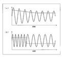
- FIG. 2 is a graph showing a time change of the oscillation signal of the oscillation circuit 11 in the capacitance sensor 1.
- FIG. 2 shows how the oscillation signal of the oscillation circuit 11 is changed by the amplitude control signal from the amplitude control circuit 13.
- a solid line and a broken line indicate voltage values of the oscillation signal and the amplitude control signal, respectively.
- the amplitude control circuit 13 decreases the amplitude of the oscillation signal and converges to a reference value.
- the amplitude control signal having such a voltage value is output to the feedback circuit 21.
- the amplitude control signal having a predetermined voltage value is output to the feedback circuit 21 so that the amplitude of the oscillation signal maintains the reference value.
- FIG. 2B shows how the oscillation signal of the oscillation circuit 11 is changed by the frequency control signal from the frequency control circuit 14.
- a solid line and a broken line indicate voltage values of the oscillation signal and the frequency control signal, respectively.
- the frequency control circuit 14 determines that the frequency control signal has such a voltage value that the oscillation frequency f OSC decreases. Is output to the feedback circuit 21.
- the oscillation frequency f OSC is expressed by the following equation using the capacitance C X of the detection electrode 2 and the variable resistance R of the variable resistance element.
- f OSC 1 / (2 ⁇ ⁇ C X ⁇ R) (1). Therefore, the frequency control circuit 14 can lower the oscillation frequency f OSC by outputting the frequency control signal to the feedback circuit 21 so as to increase the variable resistance R.
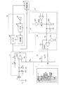
- FIG. 3 is a circuit diagram showing a schematic configuration of the capacitance sensor according to the second embodiment of the present invention.
- the capacitance sensor 1 of the present embodiment is obtained by changing the oscillation circuit 11, the amplitude control circuit 13, and the frequency control circuit 14 to a more specific configuration compared to the capacitance sensor 1 of the first embodiment.
- the other configurations are the same.
- the oscillation circuit 11 of the present embodiment is a Wien bridge type oscillation circuit.
- the Wien bridge oscillation circuit includes a band pass filter and a non-inverting amplifier circuit. Since the detailed configuration of the Wien bridge type oscillation circuit is known, its description is omitted.
- the oscillation circuit 11 includes the detection electrode 2, the operational amplifier OP21, the variable capacitance elements C 1 and C 2 , the variable resistance elements R 1 and R 2 , and the resistance elements R 3 and R 4 , and oscillates.
- the condition for the oscillation circuit 11 to oscillate is that the feedback rate C 2 ⁇ R 2 / ((C X + C 1 ) ⁇ R 2 + C 2 ⁇ R 2 + C 2 ⁇ R 1 ) at the oscillation frequency f OSC . Is equal to or higher than the negative feedback rate R 4 / (R 3 + R 4 ). R 3 / R 4 ⁇ ((C X + C 1 ) / C 2 ) + (R 1 / R 2 ) (3).
- the amplitude control circuit 13 is based on the amplitude detection circuit 31 that detects the amplitude of the oscillation signal of the oscillation circuit 11, the integration circuit 32 that integrates the output of the amplitude detection circuit 31, and the output of the integration circuit 32.
- the gain control circuit 33 controls the gain in the inverting amplifier circuit.
- Amplitude detection circuit 31 includes an operational amplifier OP 22, a current source CS1, CS2, PMOS transistors MP, configured with a capacitive element C 3.
- the operational amplifier OP22 when the voltage of the oscillation signal of the oscillation circuit 11 is equal to or higher than the voltage of the node ND1, PMOS transistor MP is turned on, the capacitance element C 3 by a current from the current source CS1 is charged.
- the operational amplifier OP22 when the voltage of the oscillation signal of the oscillation circuit 11 is smaller than the voltage of the node ND1, PMOS transistor MP is turned off, the capacitance element C 3 is discharged by the current source CS2. By repeating this operation, the amplitude detection circuit 31 can detect the amplitude of the oscillation signal of the oscillation circuit 11.
- the integrating circuit 32 includes an operational amplifier OP23, a capacitance element C 4 , a resistance element R 5 , and a reference voltage source VS1.
- the integrating circuit 32 operates as a low-pass filter, and flattens the fluctuation of the voltage of the node ND1 due to charging / discharging in the amplitude detecting circuit 31.
- the amplification factor control circuit 33 includes an NMOS transistor MN, a capacitance element C 5 , and a resistance element R 6 .
- NMOS transistor MN is inserted between the reference potential and the resistance element R 4 in the oscillation circuit 11.
- the feedback rate of the negative feedback becomes (R 4 + R MN ) / (R 3 + R 4 + R MN ) using the resistance R MN of the NMOS transistor MN, and the above equation (3) becomes the following equation.
- the capacitance elements C 5 and the resistor R 6 is used to improve the frequency characteristics of the NMOS transistor MN.
- the amplitude control circuit 13 detects the amplitude of the oscillation signal of the oscillation circuit 11 by the amplitude detection circuit 31, and the oscillation circuit so that the amplitude is equal to the voltage supplied from the reference voltage source VS1. 11 gain will be controlled. Thereby, the oscillation circuit 11 can maintain an oscillation state with a predetermined amplitude.
- the oscillation circuit 11 causes the oscillation signal amplitude to be larger than the power supply voltage and is not a sine wave. Therefore, the oscillation frequency f WIEN determined by the above equation (2). Will oscillate at a different frequency.
- the amplitude control circuit 13 controls the amplification factor of the oscillation circuit 11 so as to reduce the amplitude of the oscillation signal of the oscillation circuit 11.
- the oscillation circuit 11 can maintain the amplitude of the oscillation signal below the power supply voltage and can maintain a sine wave, and can therefore maintain the oscillation at the oscillation frequency f WIEN determined by the above equation (2).
- the frequency control circuit 14 includes a clock generator 35, a counter 36, a comparator 37, and a register 38.
- the clock generator 35 generates a clock signal having the clock frequency f CLK and outputs it to the counter 36.
- the counter 36 counts the period of the oscillation signal of the oscillation circuit 11 based on the clock signal from the clock generator 35.
- the counter 36 can easily count the period of the oscillation signal, and the oscillation frequency f that is the reciprocal of the period. WIEN can be estimated easily.
- the comparator 37 compares the count value of the counter 36 with a reference value.
- the comparator 37 changes the data in the register 38 based on the comparison result.
- the register 38 stores instruction values for the variable capacitance elements C 1 and C 2 and the variable resistance elements R 1 and R 2 in the oscillation circuit 11. Based on the indicated value, the capacitances of the variable capacitance elements C 1 and C 2 and the resistances of the variable resistance elements R 1 and R 2 in the oscillation circuit 11 are changed. Note that the register 38 may be provided in the oscillation circuit 11.
- the evaluation circuit 12 refers to the instruction value of the register 38 and grasps the changed capacitances C 1 and C 2 and the resistors R 1 and R 2 . Accordingly, even if the capacitance C 1, C 2 and a resistor R 1, R 2 is changed, it is possible to evaluate the capacitance C X of the oscillation frequency f WIEN based on the equation (2).
- the frequency control circuit 14 detects the period of the oscillation signal of the oscillation circuit 11 by the counter 36. From the above equation (2), when the capacitance C X increases, the oscillation frequency f WIEN decreases and the period of the oscillation signal increases. Therefore, the comparator 37 determines the variable capacitance elements C 1 , C 1 in the oscillation circuit 11 so that the oscillation frequency f WIEN is increased based on the equation (2) when the period of the oscillation signal exceeds the reference value. 2 and the instruction values to the variable resistance elements R 1 and R 2 are changed and stored in the register 38.
- the capacitances of the variable capacitance elements C 1 and C 2 and the resistances of the variable resistance elements R 1 and R 2 in the oscillation circuit 11 are changed, whereby the oscillation frequency f WIEN of the oscillation circuit 11 is changed. Becomes higher. Therefore, by controlling the oscillation frequency f WIEN of the oscillation circuit 11 within a predetermined range, the oscillation circuit 11 can maintain the oscillation state within the predetermined frequency range.
- FIG. 4 is a block diagram showing a schematic configuration of a capacitance sensor according to the third embodiment of the present invention.
- the capacitance sensor 1 of the present embodiment is different from the capacitance sensor 1 of the second embodiment in that the amplitude control circuit 13 and the frequency control circuit 14 are instructed to each other, and the other configurations are the same. It is.
- the circuit configuration as shown in FIG. 3 is omitted.
- the oscillation signal of the oscillation circuit 11 is required for at least 1/2 period. For this reason, when the oscillation frequency f WIEN of the oscillation circuit 11 is extremely low (the period is extremely long), it takes time to detect the amplitude and change the amplification factor.
- an upper limit value is set for the count value of the counter 36.
- the frequency control circuit 14 determines that the oscillation circuit 11 is not oscillating, and changes the amplification degree so that the oscillation circuit 11 can easily oscillate. I am instructing. Thereby, even when the oscillation frequency f WIEN is extremely low, the amplitude control circuit 13 can quickly change the amplification factor and can quickly restart the oscillation of the oscillation circuit 11.
- the frequency control circuit 14 may change the indicated value of the register 38 so that the oscillation circuit 11 can easily oscillate when the count value reaches the upper limit value. Thereby, the oscillation of the oscillation circuit 11 can be restarted more quickly.
- the NMOS transistor MN in the amplification factor control circuit 33 has frequency characteristics. Therefore, in the present embodiment, the amplitude control circuit 13 instructs the frequency control circuit 14 so that the oscillation frequency f WIEN of the oscillation circuit 11 is in a range where the NMOS transistor MN is not affected by the frequency characteristics. . Thereby, the amplitude of the oscillation signal of the oscillation circuit 11 can be accurately controlled.
- the capacitance sensor 1 of the second and third embodiments has the detection electrode 2 connected to the input side of the operational amplifier OP ⁇ b> 21 in the oscillation circuit 11. It will vibrate with a sine wave with a small amplitude. As a result, the intensity of the electromagnetic wave radiated from the detection electrode 2 is small and the band is narrow.
- the oscillation frequency f WIEN is determined by the pass band of the band-pass filter, so that the influence of noise from the outside can be suppressed.
- the capacitance sensor 1 of the above embodiment has high EMC (Electromagnetic Compatibility) resistance. Therefore, the capacitance sensor 1 of the present embodiment is suitable for use in devices that require EMC resistance, such as water level sensors, touch sensors, and proximity sensors.
- the oscillation frequency f OSC of the oscillation signal used by the evaluation circuit 12 is the reciprocal of the period of the oscillation signal counted by the counter 36 of the frequency control circuit 14. Therefore, the clock generator 35 and the counter 36 of the frequency control circuit 14 may be provided in the evaluation circuit 12. In this case, the evaluation circuit 12 evaluates the capacitance C X of the detection electrode 2 with reference to the register 38 of the frequency control circuit 14 based on the period of the oscillation signal counted by the counter 36. . Thereby, the electrostatic capacitance sensor 1 can reduce a number of parts and can be reduced in size.
- the capacitance sensor is a capacitance sensor that detects the capacitance of a detection electrode or a change thereof, and includes an amplification circuit and a predetermined frequency among signals amplified by the amplification circuit.
- An oscillation circuit that oscillates at an oscillation frequency included in the frequency band by providing a feedback circuit that feeds a signal in a band back to the amplifier circuit at a predetermined feedback rate, wherein the oscillation frequency and the feedback rate are detected
- the oscillation circuit in which the detection electrode is connected to the feedback circuit, and the amplitude of the oscillation signal that is an output signal of the oscillation circuit is less than or equal to a predetermined upper limit so as to depend on the capacitance of the electrode.
- an amplitude control circuit for controlling the feedback rate of the feedback circuit.
- the amplitude control circuit controls the feedback rate even if the feedback circuit increases the feedback rate and the amplitude of the oscillation signal of the oscillation circuit increases because the capacitance of the detection electrode changes. Then, the amplitude is maintained below a predetermined upper limit value. Thereby, it is possible to prevent the amplitude of the oscillation signal of the oscillation circuit from being too large and distorting the waveform of the oscillation signal. Thereby, since the correspondence between the capacitance and the oscillation frequency is maintained, the capacitance can be obtained from the oscillation frequency. As a result, the capacitance detection range can be expanded as compared with the conventional case.
- the capacitance sensor according to aspect 2 of the present invention is the capacitance sensor according to aspect 1, wherein the amplitude control circuit further provides feedback of the feedback circuit so that the amplitude of the oscillation signal of the oscillation circuit is equal to or greater than a predetermined lower limit value.
- the rate may be controlled. In this case, it can be prevented that the oscillation frequency of the oscillation circuit is too small to detect the oscillation frequency. As a result, the capacitance detection range can be further expanded as compared with the conventional case.
- the capacitance sensor according to Aspect 3 of the present invention is the capacitance sensor according to Aspect 1, wherein the amplitude control circuit controls the feedback rate of the feedback circuit so that the amplitude of the oscillation signal of the oscillation circuit becomes a predetermined value. Also good. In this case, since the amplitude of the oscillation signal of the oscillation circuit is maintained at a predetermined value at which the oscillation frequency is easy to detect, the oscillation frequency can be detected with high accuracy.
- An electrostatic capacity sensor is the above-described aspect 1 to 3, in which the evaluation circuit that evaluates the electrostatic capacity based on the oscillation frequency of the oscillation circuit, and the predetermined frequency band in the feedback circuit.
- the evaluation circuit that evaluates the electrostatic capacity based on the oscillation frequency of the oscillation circuit, and the predetermined frequency band in the feedback circuit.
- a frequency control circuit for controlling the feedback circuit so as to change to a frequency band including the oscillation frequency
- the evaluation circuit transmits the oscillation frequency and the frequency control circuit to the feedback circuit. It is preferable to evaluate the capacitance based on the result of the control. In this case, even if the oscillation frequency changes due to the change in the capacitance of the detection electrode, the frequency control circuit controls the feedback circuit to feed back a signal in a predetermined frequency band including the changed oscillation frequency. . Thereby, it is possible to prevent the oscillation circuit from oscillating due to a change in the capacitance of the detection electrode.
- the evaluation circuit evaluates the capacitance based on the oscillation frequency and a result of control of the frequency control circuit to the feedback circuit. Therefore, even if the predetermined frequency band is changed, the capacitance can be obtained from the oscillation frequency. As a result, the capacitance detection range can be further expanded as compared with the conventional case.
- the capacitance sensor according to Aspect 5 of the present invention is the capacitance sensor according to Aspect 4, wherein the frequency control circuit includes a clock generator and a counter that counts the period of the oscillation signal using the clock signal from the clock generator. You may prepare. In this case, the oscillation frequency that is the reciprocal of the period can be easily detected.
- the frequency control circuit when the count value of the counter is set to an upper limit value, the frequency control circuit, when the count value reaches the upper limit value, The amplitude control circuit may be instructed to change the amplification degree of the oscillation circuit. In this case, even when the oscillation frequency is extremely low, the amplitude control circuit can quickly change the amplification factor and can quickly resume the oscillation of the oscillation circuit.
- the capacitance sensor according to aspect 7 of the present invention is the capacitance sensor according to any one of the aspects 4 to 6, wherein the frequency control circuit is configured to maintain the oscillation frequency in a range in which the amplitude control circuit is not affected by frequency characteristics.
- the circuit may be controlled.
- the amplitude control circuit can accurately control the amplitude of the oscillation signal of the oscillation circuit.
- the capacitance sensor according to the present invention maintains the amplitude below a predetermined upper limit even when the amplitude of the oscillation signal of the oscillation circuit increases due to the change in capacitance of the detection electrode. Therefore, the waveform of the oscillation signal can be prevented from being distorted, and the capacitance detection range can be expanded as compared with the prior art. Therefore, the present invention can be applied to any capacitance sensor using an oscillator.
Landscapes
- Measurement Of Resistance Or Impedance (AREA)
Abstract
発振回路(11)では、演算増幅器(OP1)が増幅した信号のうち、所定の周波数帯域の信号を所定の帰還率で帰還回路(21)が演算増幅器(OP1)に帰還し、帰還回路(21)に検出電極(2)が接続されている。振幅制御回路(13)は、発振回路(11)の出力信号の振幅が所定の上限値以下となるように、帰還回路(21)の帰還率を制御する。
Description
本発明は、検出電極の静電容量又はその変化を検出する静電容量センサに関し、特に、発振回路を用いた静電容量センサに関する。
従来、静電容量の変化を検出することにより物体の接近を検知する静電容量形近接センサが知られており、例えば、特許文献1には、上記静電容量形近接センサを用いて、流体の有無、構成、状態変化などを検知する流体検知センサが開示されている。
上記静電容量形近接センサは、上記静電容量の変化を検出する回路として発振回路を備えており、該発振回路の一部が検出電極となっている。上記発振回路は、上記物体が接近すると、上記検出電極の静電容量CXが増加して、発振周波数fOSCが変化する。そして、上記静電容量形近接センサは、上記発振回路の発振周波数fOSCが所定の基準値に達したか否かを判定する判定回路を備えており、該判定の結果により、上記物体の接近を検知することができる。
図5は、上記静電容量形近接センサの概略構成を示す回路図である。図示のように、静電容量形近接センサ101は、発振回路111及び判定回路112を備えている。図示の例では、発振回路111は、検出電極113と、演算増幅器A、静電容量素子C2、及び抵抗素子R1~R4とを備えたウィーンブリッジ型発振回路である。該ウィーンブリッジ型発振回路の発振周波数fOSCは次式で表される。
fOSC=(2π×(CX×C2×R1×R2)1/2)-1 ・・・(a)。
なお、本願では、抵抗素子の符号は、それぞれ、抵抗素子の抵抗値でもあり、静電容量素子の符号は、静電容量素子の容量でもある。
fOSC=(2π×(CX×C2×R1×R2)1/2)-1 ・・・(a)。
なお、本願では、抵抗素子の符号は、それぞれ、抵抗素子の抵抗値でもあり、静電容量素子の符号は、静電容量素子の容量でもある。
従って、静電容量CXが減少すると、発振周波数fOSCは増加する。発振回路111は、上記式(a)を満たす発振周波数fOSCの信号を判定回路112に出力する。
また、発振回路113が発振するための条件は、発振周波数fOSCにおいて、正帰還の帰還率C2×R2/(CX×R2+C2×R2+C2×R1)が、負帰還の帰還率R4/(R3+R4)以上となることであり、整理すると次式で表される。
R3/R4≧(CX/C2)+(R1/R2) ・・・(b)。
R3/R4≧(CX/C2)+(R1/R2) ・・・(b)。
判定回路112は、発振回路111からの信号の発振周波数fOSCの変化を監視し、目的に応じて所要の信号に変換して出力するものである。例えば、判定回路112は、発振周波数fOSCを直流電圧に変換する周期/電圧変換回路、変換した直流電圧を所定の基準値と比較するコンパレータ、上記直流電圧が上記基準値よりも大きい又は小さい場合に、所定の警報を発したり制御信号を発したりする出力回路、などで構成される。
従来の上記静電容量形近接センサ101の場合、流体が有るとき、または流体が無いときにおける検出電極113の静電容量CXを基準静電容量CX0とし、検出した静電容量
CXが基準静電容量CX0とどの程度相違するかを調べればよい。すなわち、基準静電容量CX0に対応する発振回路111の発振周波数fOSCを基準発振周波数fOSC0とし、検出した発振周波数fOSCと基準発振周波数fOSC0との差を求めればよい。従って、従来の上記静電容量形近接センサ101の場合、検出すべき静電容量CXの範囲は、基準静電容量CX0およびその近傍であればよく、検出可能な発振周波数fOSCの範囲は、基準発振周波数fOSC0とおよびその近傍であればよい。
CXが基準静電容量CX0とどの程度相違するかを調べればよい。すなわち、基準静電容量CX0に対応する発振回路111の発振周波数fOSCを基準発振周波数fOSC0とし、検出した発振周波数fOSCと基準発振周波数fOSC0との差を求めればよい。従って、従来の上記静電容量形近接センサ101の場合、検出すべき静電容量CXの範囲は、基準静電容量CX0およびその近傍であればよく、検出可能な発振周波数fOSCの範囲は、基準発振周波数fOSC0とおよびその近傍であればよい。
従来の静電容量形近接センサ101を、静電容量を検出する静電容量センサとして利用するには、静電容量CXの検出範囲を拡大する必要がある。しかしながら、この場合、下記の問題点が発生する。すなわち、静電容量CXが増加するにつれて、上記式(a)のように発振回路113の発振周波数fOSCが低くなると共に、上記正帰還の帰還率が小さくなることにより増幅度が小さくなり、ついには上記式(b)を満たさなくなって、発振しなくなる。一方、静電容量CXが減少するにつれて、発振回路113の発振周波数fOSCが高くなると共に、上記正帰還の帰還率が大きくなることにより増幅度が大きくなり、その結果正弦波の波形が歪むことになり、上記式(a)を満たさなくなる。
本発明は、上記の問題点に鑑みてなされたものであって、その目的は、静電容量の検出範囲が従来よりも拡大された静電容量センサを提供することにある。
本発明に係る静電容量センサは、検出電極の静電容量又はその変化を検出する静電容量センサであって、上記課題を解決するために、増幅回路と、該増幅回路が増幅した信号のうち、所定の周波数帯域の信号を所定の帰還率で前記増幅回路に帰還する帰還回路とを備えることにより、当該周波数帯域に含まれる発振周波数で発振する発振回路であって、前記発振周波数及び前記帰還率が前記検出電極の静電容量に依存するように、前記検出電極が前記帰還回路に接続された発振回路と、該発振回路の出力信号である発振信号の振幅が所定の上限値以下となるように、前記帰還回路の帰還率を制御する振幅制御回路とを備えることを特徴としている。
上記の構成によると、検出電極の静電容量が変化することにより、発振回路の発振信号の振幅が増加しても、当該振幅を所定の上限値以下に維持するので、当該発振信号の波形が歪むことを防止でき、その結果、静電容量の検出範囲を従来よりも拡大できるという効果を奏する。
本発明の実施形態について、図1~図4に基づいて説明すれば、以下のとおりである。なお、説明の便宜上、各実施形態に示した部材と同一の機能を有する部材については、同一の符号を付記し、適宜その説明を省略する。
〔実施形態1〕
(静電容量センサの構成)
図1は、本発明の第1実施形態に係る静電容量センサの概略構成を示すブロック図である。静電容量センサ1は、検出電極2の静電容量CXを検出するものであり、例えば、水位センサ、タッチセンサ、近接センサなどに利用される。図1に示すように、静電容量センサ1は、上記の検出電極2と、発振回路11、評価回路12、振幅制御回路13、及び周波数制御回路14を備える。
(静電容量センサの構成)
図1は、本発明の第1実施形態に係る静電容量センサの概略構成を示すブロック図である。静電容量センサ1は、検出電極2の静電容量CXを検出するものであり、例えば、水位センサ、タッチセンサ、近接センサなどに利用される。図1に示すように、静電容量センサ1は、上記の検出電極2と、発振回路11、評価回路12、振幅制御回路13、及び周波数制御回路14を備える。
発振回路11は、演算増幅器OP1と、該演算増幅器OP1が増幅した信号のうち、所定の周波数帯域の信号を所定の帰還率で演算増幅器OP1に帰還する帰還回路21とを備えることにより、当該周波数帯域に含まれる発振周波数fOSCで発振するものである。本実施形態では、発振周波数fOSC及び上記帰還率が検出電極2の静電容量CXに依存するように、検出電極2が帰還回路21に接続されている。
評価回路12は、発振回路11の発振周波数fOSCに基づいて、検出電極2の静電容量CXを評価するものである。
振幅制御回路13は、発振回路11の出力信号である発振信号の振幅が所定の上限値以下かつ所定の下限値以上、すなわち所定範囲となるように、帰還回路21の帰還率を制御するものである。これにより、検出電極2の静電容量CXが変化することにより、帰還回路21の帰還率が変化して、発振回路11の発振信号の振幅が増加しても、振幅制御回路13が上記帰還率を制御して、当該振幅を所定の上限値以下に維持する。従って、発振回路11の発振信号の振幅が大き過ぎて、当該発振信号の波形が歪むことを防止できる。これにより、静電容量CXと発振周波数fOSCとの対応関係が維持されるので、評価回路12は、発振周波数fOSCから静電容量CXを評価することができる。その結果、静電容量CXの検出範囲を従来よりも拡大することができる。
また、検出電極2の静電容量CXが変化することにより、帰還回路21の帰還率が変化して、発振回路11の発振信号の振幅が減少しても、振幅制御回路13が上記帰還率を制御して、当該振幅を所定の下限値以上に維持する。従って、発振回路11の発振信号の振幅が小さ過ぎて、発振周波数fOSCが検出できないことを防止できる。その結果、静電容量CXの検出範囲を従来よりもさらに拡大することができる。
なお、上記所定範囲は、発振周波数fOSCが検出し易い所定値であってもよい。この場合、発振周波数fOSCを精度良く検出することができる。
周波数制御回路14は、帰還回路21における上記所定の周波数帯域を、発振周波数fOSCを含む周波数帯域に変更するように、帰還回路21を制御するものである。これにより、検出電極2の静電容量CXが変化することにより、発振周波数fOSCが変化しても、変化した発振周波数fOSCを含む所定の周波数帯域の信号を帰還回路21が帰還するように、周波数制御回路14が帰還回路21に指示する。従って、検出電極2の静電容量CXが変化することにより、発振回路11が発振しなくなることを防止できる。
なお、上記所定の周波数帯域を変更すると、静電容量CXと発振周波数fOSCとの対応関係も変化する。そこで、本実施形態では、評価回路12は、発振周波数fOSCと、周波数制御回路14の帰還回路21への指示とに基づいて、静電容量CXを評価する。これにより、上記所定の周波数帯域を変更しても、発振周波数fOSCから静電容量CXを求めることができる。その結果、静電容量CXの検出範囲を従来よりもさらに拡大することができる。
(静電容量センサの動作)
この点を、図2を参照して具体的に説明する。図2は、静電容量センサ1における発振回路11の発振信号の時間変化を示すグラフである。
この点を、図2を参照して具体的に説明する。図2は、静電容量センサ1における発振回路11の発振信号の時間変化を示すグラフである。
図2の(a)は、振幅制御回路13からの振幅制御信号により、発振回路11の発振信号がどのように変化するかを示している。同図において、実線及び破線は、それぞれ、上記発振信号及び上記振幅制御信号の電圧値を示している。
図2の(a)に示すように、静電容量CXが小さくなり上記発振信号の振幅が大きくなった場合、振幅制御回路13は、上記発振信号の振幅が小さくなって基準値に収束するような電圧値の上記振幅制御信号を帰還回路21に出力する。そして、上記発振信号の振幅が基準値と等しくなった後は、上記発振信号の振幅が基準値を維持するように、所定の電圧値の上記振幅制御信号を帰還回路21に出力する。
一方、図2の(b)は、周波数制御回路14からの周波数制御信号により、発振回路11の発振信号がどのように変化するかを示している。同図において、実線及び破線は、それぞれ、上記発振信号及び上記周波数制御信号の電圧値を示している。図示のように、静電容量CXが小さくなり上記発振信号の発振周波数fOSCが高くなった場合、周波数制御回路14は、上記発振周波数fOSCが低くなるような電圧値の上記周波数制御信号を帰還回路21に出力する。
ここで、発振回路11がCR発振回路である場合、発振周波数fOSCは、検出電極2の静電容量CXと可変抵抗素子の可変抵抗Rとを用いて次式で表される。
fOSC=1/(2π×CX×R) ・・・(1)。
従って、周波数制御回路14は、可変抵抗Rを大きくするように、上記周波数制御信号を帰還回路21に出力することにより、発振周波数fOSCを低くすることができる。
fOSC=1/(2π×CX×R) ・・・(1)。
従って、周波数制御回路14は、可変抵抗Rを大きくするように、上記周波数制御信号を帰還回路21に出力することにより、発振周波数fOSCを低くすることができる。
〔実施形態2〕
図3は、本発明の第2実施形態に係る静電容量センサの概略構成を示す回路図である。本実施形態の静電容量センサ1は、第1実施形態の静電容量センサ1に比べて、発振回路11、振幅制御回路13、及び周波数制御回路14を、より具体的な構成に変更している点が異なり、その他の構成は同様である。
図3は、本発明の第2実施形態に係る静電容量センサの概略構成を示す回路図である。本実施形態の静電容量センサ1は、第1実施形態の静電容量センサ1に比べて、発振回路11、振幅制御回路13、及び周波数制御回路14を、より具体的な構成に変更している点が異なり、その他の構成は同様である。
(発振回路の構成)
本実施形態の発振回路11は、ウィーンブリッジ型発振回路である。ウィーンブリッジ型発振回路は、バンドパスフィルタと非反転増幅回路とを備える構成である。なお、ウィーンブリッジ型発振回路の詳細な構成は公知であるので、その説明を省略する。
本実施形態の発振回路11は、ウィーンブリッジ型発振回路である。ウィーンブリッジ型発振回路は、バンドパスフィルタと非反転増幅回路とを備える構成である。なお、ウィーンブリッジ型発振回路の詳細な構成は公知であるので、その説明を省略する。
これにより、発振回路11は、検出電極2、演算増幅器OP21、可変静電容量素子C1,C2、可変抵抗素子R1,R2、及び抵抗素子R3,R4を備える構成となり、発振周波数fWIENは、次式のようになる。
fWIEN=(2π×((CX+C1)×C2×R1×R2)1/2)-1 ・・・(2)。
fWIEN=(2π×((CX+C1)×C2×R1×R2)1/2)-1 ・・・(2)。
また、発振回路11が発振するための条件は、発振周波数fOSCにおいて正帰還の帰還率C2×R2/((CX+C1)×R2+C2×R2+C2×R1)が負帰還の帰還率R4/(R3+R4)以上となることであり、整理すると次式で表される。
R3/R4≧((CX+C1)/C2)+(R1/R2) ・・・(3)。
R3/R4≧((CX+C1)/C2)+(R1/R2) ・・・(3)。
(振幅制御回路の構成)
振幅制御回路13は、発振回路11の発振信号の振幅を検出する振幅検出回路31と、振幅検出回路31の出力を積分する積分回路32と、積分回路32の出力に基づき、発振回路11の非反転増幅回路における増幅率を制御する増幅率制御回路33とを備える構成である。
振幅制御回路13は、発振回路11の発振信号の振幅を検出する振幅検出回路31と、振幅検出回路31の出力を積分する積分回路32と、積分回路32の出力に基づき、発振回路11の非反転増幅回路における増幅率を制御する増幅率制御回路33とを備える構成である。
振幅検出回路31は、演算増幅器OP22、電流源CS1,CS2、PMOSトランジスタMP、静電容量素子C3を備える構成である。演算増幅器OP22は、発振回路11の発振信号の電圧がノードND1の電圧以上である時、PMOSトランジスタMPがオンになり、電流源CS1からの電流で静電容量素子C3は充電される。また、演算増幅器OP22は、発振回路11の発振信号の電圧がノードND1の電圧より小さい時、PMOSトランジスタMPがオフになり、静電容量素子C3は電流源CS2により放電される。この動作を繰り返すことにより、振幅検出回路31は発振回路11の発振信号の振幅を検出できる。
積分回路32は、演算増幅器OP23、静電容量素子C4、抵抗素子R5、及び基準電圧源VS1を備える構成である。積分回路32は、ローパスフィルタとして動作し、振幅検出回路31での充放電によるノードND1の電圧の揺れを平坦化する。
増幅率制御回路33は、NMOSトランジスタMN、静電容量素子C5、及び抵抗素子R6を備える構成である。NMOSトランジスタMNは、発振回路11における抵抗素子R4と参照電位との間に挿入される。これにより、負帰還の帰還率は、NMOSトランジスタMNの抵抗RMNを用いて、(R4+RMN)/(R3+R4+RMN)となり、上記式(3)は次式となる。
R3/(R4+RMN)≧((CX+C1)/C2)+(R1/R2) ・・・(4)。
R3/(R4+RMN)≧((CX+C1)/C2)+(R1/R2) ・・・(4)。
従って、静電容量CXが大きくなっても、RMNを小さくすることにより、上記式(4)を満たすことができ、発振条件を維持できる。なお、静電容量素子C5及び抵抗素子R6は、NMOSトランジスタMNの周波数特性を改善するために使用される。
上記の構成によると、振幅制御回路13は、振幅検出回路31にて発振回路11の発振信号の振幅を検出し、当該振幅が基準電圧源VS1にて供給される電圧と等しくなるように発振回路11の増幅率を制御することになる。これにより、発振回路11は、所定の振幅で発振状態を維持することができる。
一方、静電容量CXが小さくなると正帰還の帰還率は大きくなって、発振回路11の増幅率が大きくなる。このことから、静電容量CXが小さくなり過ぎると、発振回路11は、発振信号の振幅が電源電圧よりも大きくなって正弦波ではなくなるため、上記式(2)で決められる発振周波数fWIENとは異なる周波数で発振することになる。
これに対し、振幅制御回路13は、発振回路11の発振信号の振幅を小さくするように発振回路11の増幅率を制御する。これにより、発振回路11は、発振信号の振幅が電源電圧以下に維持できて、正弦波を維持できるため、上記式(2)で決められる発振周波数fWIENでの発振を維持できる。
(周波数制御回路の構成)
周波数制御回路14は、クロック生成器35、カウンタ36、比較器37、及びレジスタ38を備える構成である。
周波数制御回路14は、クロック生成器35、カウンタ36、比較器37、及びレジスタ38を備える構成である。
クロック生成器35は、クロック周波数fCLKのクロック信号を生成し、カウンタ36に出力する。カウンタ36は、クロック生成器35からのクロック信号に基づいて、発振回路11の発振信号の周期を計数する。クロック生成器35のクロック周波数fCLKを発振回路11の発振周波数よりも十分高くしておくことで、カウンタ36は、上記発振信号の周期を簡便に計数でき、該周期の逆数である発振周波数fWIENを簡便に推定することができる。
比較器37は、カウンタ36の計数値を基準値と比較する。比較器37は、比較結果に基づき、レジスタ38のデータを変更する。レジスタ38は、発振回路11における可変静電容量素子C1,C2及び可変抵抗素子R1,R2への指示値を記憶する。該指示値に基づき、発振回路11における可変静電容量素子C1,C2の容量と、可変抵抗素子R1,R2の抵抗とが変更される。なお、レジスタ38は、発振回路11に設けられていてもよい。
評価回路12は、レジスタ38の指示値を参照して、変更後の容量C1,C2及び抵抗R1,R2を把握する。これにより、容量C1,C2及び抵抗R1,R2が変更されても、上記式(2)に基づき発振周波数fWIENから静電容量CXを評価することができる。
ところで、静電容量CXが大きくなると、上記式(3)又は(4)が満たされなくなるため、発振回路11が発振状態を維持できなくなり、静電容量CXを推定できなくなる。
これに対し、周波数制御回路14は、カウンタ36にて発振回路11の発振信号の周期を検出する。上記式(2)より、静電容量CXが大きくなると、発振周波数fWIENが低くなり、上記発振信号の周期が大きくなる。そこで、比較器37は、上記発振信号の周期が基準値を超える場合、上記式(2)に基づき、発振周波数fWIENが高くなるように、発振回路11における可変静電容量素子C1,C2及び可変抵抗素子R1,R2への指示値を変更し、レジスタ38に記憶する。該指示値に基づき、発振回路11における可変静電容量素子C1,C2の容量と、可変抵抗素子R1,R2の抵抗とが変更されることにより、発振回路11の発振周波数fWIENが高くなる。従って、発振回路11の発振周波数fWIENを所定範囲内に制御することで、発振回路11は、所定の周波数範囲で発振状態を維持することができる。
〔実施形態3〕
図4は、本発明の第3実施形態に係る静電容量センサの概略構成を示すブロック図である。本実施形態の静電容量センサ1は、第2実施形態の静電容量センサ1に比べて、振幅制御回路13及び周波数制御回路14の間で互いに指示される点が異なり、その他の構成は同様である。なお、図4では、図3に示すような回路構成を省略している。
図4は、本発明の第3実施形態に係る静電容量センサの概略構成を示すブロック図である。本実施形態の静電容量センサ1は、第2実施形態の静電容量センサ1に比べて、振幅制御回路13及び周波数制御回路14の間で互いに指示される点が異なり、その他の構成は同様である。なお、図4では、図3に示すような回路構成を省略している。
振幅制御回路13は、振幅を検出するには、発振回路11の発振信号が少なくとも1/2周期分必要である。このため、発振回路11の発振周波数fWIENが著しく低い(周期が著しく長い)場合、振幅を検出して増幅率を変更するまでに時間がかかることになる。
そこで、本実施形態の周波数制御回路14では、カウンタ36の計数値に上限値が設定されている。該計数値が上限値に達した場合、周波数制御回路14は、発振回路11が発振していないと判断し、増幅度を変更して発振回路11が発振し易くなるように振幅制御回路13に指示している。これにより、振幅制御回路13は、発振周波数fWIENが著しく低い場合でも、迅速に増幅率を変更して、発振回路11の発振を迅速に再開させることができる。
さらに、周波数制御回路14は、上記計数値が上限値に達した場合、発振回路11が発振し易くなるように、レジスタ38の指示値を変更してもよい。これにより、発振回路11の発振をさらに迅速に再開させることができる。
また、振幅制御回路13では、増幅率制御回路33におけるNMOSトランジスタMNが周波数特性を有している。そこで、本実施形態では、振幅制御回路13は、発振回路11の発振周波数fWIENが、NMOSトランジスタMNが上記周波数特性の影響を受けない範囲となるように、周波数制御回路14に指示している。これにより、発振回路11の発振信号の振幅を精度よく制御することができる。
〔付記事項〕
第2・第3実施形態の静電容量センサ1は、図3に示すように、検出電極2が発振回路11における演算増幅器OP21の入力側に接続されていることから、検出電極2の電位は振幅の小さい正弦波で振動することになる。その結果、検出電極2から外部に放射される電磁波の強度は小さく、かつ帯域は狭い。また、ウィーンブリッジ型発振回路の場合、発振周波数fWIENは、上記バンドパスフィルタの通過帯域で決定されるため、外部からのノイズの影響を抑制することができる。以上から、上記実施形態の静電容量センサ1は、EMC(Electromagnetic Compatibility)の耐性が高い。従って、本実施形態の静電容量センサ1は、EMCの耐性が求められる機器、例えば水位センサ、タッチセンサ、近接センサでの利用に好適である。
第2・第3実施形態の静電容量センサ1は、図3に示すように、検出電極2が発振回路11における演算増幅器OP21の入力側に接続されていることから、検出電極2の電位は振幅の小さい正弦波で振動することになる。その結果、検出電極2から外部に放射される電磁波の強度は小さく、かつ帯域は狭い。また、ウィーンブリッジ型発振回路の場合、発振周波数fWIENは、上記バンドパスフィルタの通過帯域で決定されるため、外部からのノイズの影響を抑制することができる。以上から、上記実施形態の静電容量センサ1は、EMC(Electromagnetic Compatibility)の耐性が高い。従って、本実施形態の静電容量センサ1は、EMCの耐性が求められる機器、例えば水位センサ、タッチセンサ、近接センサでの利用に好適である。
また、評価回路12が利用する発振信号の発振周波数fOSCは、周波数制御回路14のカウンタ36が計数する上記発振信号の周期の逆数である。そこで、周波数制御回路14のクロック生成器35及びカウンタ36を、評価回路12に設けてもよい。この場合、評価回路12は、カウンタ36にて計数された上記発振信号の周期に基づき、周波数制御回路14のレジスタ38を参照して、検出電極2の静電容量CXを評価することになる。これにより、静電容量センサ1は、部品点数を削減することができ、小型化することができる。
本発明は上述した各実施形態に限定されるものではなく、請求項に示した範囲で種々の変更が可能であり、異なる実施形態にそれぞれ開示された技術的手段を適宜組み合わせて得られる実施形態についても本発明の技術的範囲に含まれる。さらに、各実施形態にそれぞれ開示された技術的手段を組み合わせることにより、新しい技術的特徴を形成することができる。
〔まとめ〕
本発明の態様1に係る静電容量センサは、検出電極の静電容量又はその変化を検出する静電容量センサであって、増幅回路と、該増幅回路が増幅した信号のうち、所定の周波数帯域の信号を所定の帰還率で前記増幅回路に帰還する帰還回路とを備えることにより、当該周波数帯域に含まれる発振周波数で発振する発振回路であって、前記発振周波数及び前記帰還率が前記検出電極の静電容量に依存するように、前記検出電極が前記帰還回路に接続された発振回路と、該発振回路の出力信号である発振信号の振幅が所定の上限値以下となるように、前記帰還回路の帰還率を制御する振幅制御回路とを備える構成である。
本発明の態様1に係る静電容量センサは、検出電極の静電容量又はその変化を検出する静電容量センサであって、増幅回路と、該増幅回路が増幅した信号のうち、所定の周波数帯域の信号を所定の帰還率で前記増幅回路に帰還する帰還回路とを備えることにより、当該周波数帯域に含まれる発振周波数で発振する発振回路であって、前記発振周波数及び前記帰還率が前記検出電極の静電容量に依存するように、前記検出電極が前記帰還回路に接続された発振回路と、該発振回路の出力信号である発振信号の振幅が所定の上限値以下となるように、前記帰還回路の帰還率を制御する振幅制御回路とを備える構成である。
上記の構成によると、検出電極の静電容量が変化することにより、帰還回路の帰還率が増加して、発振回路の発振信号の振幅が増加しても、振幅制御回路が上記帰還率を制御して、当該振幅を所定の上限値以下に維持する。これにより、発振回路の発振信号の振幅が大き過ぎて、当該発振信号の波形が歪むことを防止できる。これにより、静電容量と発振周波数との対応関係が維持されるので、発振周波数から静電容量を求めることができる。
その結果、静電容量の検出範囲を従来よりも拡大することができる。
その結果、静電容量の検出範囲を従来よりも拡大することができる。
本発明の態様2に係る静電容量センサは、上記態様1において、前記振幅制御回路は、さらに、前記発振回路の発振信号の振幅が所定の下限値以上となるように、前記帰還回路の帰還率を制御してもよい。この場合、上記発振回路の発振信号の振幅が小さ過ぎて、上記発振周波数が検出できないことを防止できる。その結果、静電容量の検出範囲を従来よりもさらに拡大することができる。
本発明の態様3に係る静電容量センサは、上記態様1において、前記振幅制御回路は、前記発振回路の発振信号の振幅が所定値となるように、前記帰還回路の帰還率を制御してもよい。この場合、上記発振回路の発振信号の振幅が、上記発振周波数が検出し易い所定値に維持されることにより、当該発振周波数を精度良く検出することができる。
本発明の態様4に係る静電容量センサは、上記態様1から3において、前記発振回路の発振周波数に基づいて、前記静電容量を評価する評価回路と、前記帰還回路における前記所定の周波数帯域を、前記発振周波数を含む周波数帯域に変更するように、前記帰還回路を制御する周波数制御回路とをさらに備えており、前記評価回路は、前記発振周波数と、前記周波数制御回路から前記帰還回路への制御の結果とに基づいて、前記静電容量を評価することが好ましい。この場合、検出電極の静電容量が変化することにより、発振周波数が変化しても、変化した発振周波数を含む所定の周波数帯域の信号を帰還回路が帰還するように、周波数制御回路が制御する。これにより、検出電極の静電容量が変化することにより、上記発振回路が発振しなくなることを防止できる。
なお、上記所定の周波数帯域を変更すると、上記静電容量と上記発振周波数との対応関係も変化する。そこで、評価回路は、上記発振周波数と、上記周波数制御回路の上記帰還回路への制御の結果とに基づいて、上記静電容量を評価する。これにより、上記所定の周波数帯域を変更しても、発振周波数から静電容量を求めることができる。その結果、静電容量の検出範囲を従来よりもさらに拡大することができる。
本発明の態様5に係る静電容量センサは、上記態様4において、前記周波数制御回路は、クロック生成器と、該クロック生成器からのクロック信号で、前記発振信号の周期を計数するカウンタとを備えてもよい。この場合、上記周期の逆数である上記発振周波数を簡便に検出することができる。
本発明の態様6に係る静電容量センサは、上記態様5において、前記カウンタの計数値に上限値が設定されており、前記周波数制御回路は、該計数値が上限値に達した場合、前記発振回路の増幅度を変更するように前記振幅制御回路に指示してもよい。この場合、上記振幅制御回路は、上記発振周波数が著しく低い場合でも、迅速に増幅率を変更して、上記発振回路の発振を迅速に再開させることができる。
本発明の態様7に係る静電容量センサは、上記態様4から6において、前記周波数制御回路は、前記振幅制御回路が周波数特性の影響を受けない範囲に前記発振周波数を維持するように前記発振回路を制御してもよい。この場合、上記振幅制御回路は、上記発振回路の発振信号の振幅を精度よく制御することができる。
以上のように、本発明に係る静電容量センサは、検出電極の静電容量が変化することにより、発振回路の発振信号の振幅が増加しても、当該振幅を所定の上限値以下に維持するので、当該発振信号の波形が歪むことを防止でき、静電容量の検出範囲を従来よりも拡大できるので、発振器を利用した任意の静電容量センサに本発明を適用することができる。
1 静電容量センサ
2 検出電極
11 発振回路
12 評価回路
13 振幅制御回路
14 周波数制御回路
21 帰還回路
31 振幅検出回路
32 積分回路
33 増幅率制御回路
35 クロック生成器
36 カウンタ
37 比較器
38 レジスタ
OP1・OP21 演算増幅器
2 検出電極
11 発振回路
12 評価回路
13 振幅制御回路
14 周波数制御回路
21 帰還回路
31 振幅検出回路
32 積分回路
33 増幅率制御回路
35 クロック生成器
36 カウンタ
37 比較器
38 レジスタ
OP1・OP21 演算増幅器
Claims (5)
- 検出電極の静電容量又はその変化を検出する静電容量センサであって、
増幅回路と、該増幅回路が増幅した信号のうち、所定の周波数帯域の信号を所定の帰還率で前記増幅回路に帰還する帰還回路とを備えることにより、当該周波数帯域に含まれる発振周波数で発振する発振回路であって、前記発振周波数及び前記帰還率が前記検出電極の静電容量に依存するように、前記検出電極が前記帰還回路に接続された発振回路と、
該発振回路の出力信号である発振信号の振幅が所定の上限値以下となるように、前記帰還回路の帰還率を制御する振幅制御回路とを備えることを特徴とする静電容量センサ。 - 前記振幅制御回路は、さらに、前記発振回路の発振信号の振幅が所定の下限値以上となるように、前記帰還回路の帰還率を制御することを特徴とする請求項1に記載の静電容量センサ。
- 前記振幅制御回路は、前記発振回路の発振信号の振幅が所定値となるように、前記帰還回路の帰還率を制御することを特徴とする請求項1に記載の静電容量センサ。
- 前記発振回路の発振周波数に基づいて、前記静電容量を評価する評価回路と、
前記帰還回路における前記所定の周波数帯域を、前記発振周波数を含む周波数帯域に変更するように、前記帰還回路を制御する周波数制御回路とをさらに備えており、
前記評価回路は、前記発振周波数と、前記周波数制御回路から前記帰還回路への制御の結果とに基づいて、前記静電容量を評価することを特徴とする請求項1から3までの何れか1項に記載の静電容量センサ。 - 前記周波数制御回路は、クロック生成器と、該クロック生成器からのクロック信号で、前記発振信号の周期を計数するカウンタとを備えることを特徴とする請求項4に記載の静電容量センサ。
Applications Claiming Priority (2)
| Application Number | Priority Date | Filing Date | Title |
|---|---|---|---|
| JP2013104371 | 2013-05-16 | ||
| JP2013-104371 | 2013-05-16 |
Publications (1)
| Publication Number | Publication Date |
|---|---|
| WO2014185241A1 true WO2014185241A1 (ja) | 2014-11-20 |
Family
ID=51898221
Family Applications (1)
| Application Number | Title | Priority Date | Filing Date |
|---|---|---|---|
| PCT/JP2014/061480 Ceased WO2014185241A1 (ja) | 2013-05-16 | 2014-04-23 | 静電容量センサ |
Country Status (1)
| Country | Link |
|---|---|
| WO (1) | WO2014185241A1 (ja) |
Citations (3)
| Publication number | Priority date | Publication date | Assignee | Title |
|---|---|---|---|---|
| JPH11230815A (ja) * | 1998-02-16 | 1999-08-27 | Tatsuta Electric Wire & Cable Co Ltd | 流体検知センサ |
| JP2001345696A (ja) * | 2000-05-30 | 2001-12-14 | Oki Electric Ind Co Ltd | チューニング回路 |
| JP2007006284A (ja) * | 2005-06-24 | 2007-01-11 | Calsonic Kansei Corp | ウィーンブリッジ発振回路 |
-
2014
- 2014-04-23 WO PCT/JP2014/061480 patent/WO2014185241A1/ja not_active Ceased
Patent Citations (3)
| Publication number | Priority date | Publication date | Assignee | Title |
|---|---|---|---|---|
| JPH11230815A (ja) * | 1998-02-16 | 1999-08-27 | Tatsuta Electric Wire & Cable Co Ltd | 流体検知センサ |
| JP2001345696A (ja) * | 2000-05-30 | 2001-12-14 | Oki Electric Ind Co Ltd | チューニング回路 |
| JP2007006284A (ja) * | 2005-06-24 | 2007-01-11 | Calsonic Kansei Corp | ウィーンブリッジ発振回路 |
Similar Documents
| Publication | Publication Date | Title |
|---|---|---|
| JP5280449B2 (ja) | 基準周波数生成回路、半導体集積回路、電子機器 | |
| JP5357461B2 (ja) | 近接センサ | |
| CN102753936B (zh) | 振动型惯性力传感器 | |
| US20110267078A1 (en) | Current Sensor Capacity Measuring System | |
| CN113258916B (zh) | 电容触摸检测电路、芯片和电子设备 | |
| CN108136442B (zh) | 压电致动器驱动电路 | |
| CN101257252B (zh) | 电压控制电路 | |
| US8860518B1 (en) | Current-feedback operational-amplifier based relaxation oscillator | |
| JP2018082325A (ja) | 三角波生成回路、並びに、ファンモータ電流検出装置 | |
| WO2014185241A1 (ja) | 静電容量センサ | |
| US8044735B2 (en) | Oscillator circuit and method for influencing, controlling, or regulating the frequency of an oscillator | |
| US9602002B2 (en) | Switching power supply device | |
| CN103412340B (zh) | 一种金属探测器 | |
| CN112082617A (zh) | 具有偏移补偿的电容式纱线传感器装置 | |
| JP5876250B2 (ja) | 電磁石コイルの駆動装置 | |
| CN108123682B (zh) | 振荡装置 | |
| US20180301920A1 (en) | Mems device | |
| US11340129B2 (en) | Capacitive pressure measurement device with varying frequency | |
| CN111030598B (zh) | 一种具有振荡限幅功能的晶体振荡器电路 | |
| CN113162552B (zh) | 一种电容接近开关及其扩展频谱脉冲驱动电路 | |
| JP5877091B2 (ja) | クロック供給回路 | |
| RU2725261C1 (ru) | Датчик линейного ускорения | |
| KR20110039822A (ko) | 히스테리시스 보상 기능을 갖는 고주파 발진형 근접센서 | |
| KR20050033145A (ko) | 주파수 조절이 가능한 저전압 발진회로 | |
| JP5806604B2 (ja) | 磁場検出回路 |
Legal Events
| Date | Code | Title | Description |
|---|---|---|---|
| 121 | Ep: the epo has been informed by wipo that ep was designated in this application |
Ref document number: 14798577 Country of ref document: EP Kind code of ref document: A1 |
|
| NENP | Non-entry into the national phase |
Ref country code: DE |
|
| 122 | Ep: pct application non-entry in european phase |
Ref document number: 14798577 Country of ref document: EP Kind code of ref document: A1 |
|
| NENP | Non-entry into the national phase |
Ref country code: JP |