BACKGROUND
1. Field of the Disclosure
The exemplary implementations described herein relate to a current-feedback operational-amplifier based relaxation oscillator as a versatile electronic interface for capacitive and resistive sensors.
2. Description of the Related Art
Oscillators are widely used as electronic interface for sensors. This is attributed to their simplicity and immunity to electromagnetic interference. While harmonic oscillators, widely used for capacitive and inductive sensors, have a very high sensitivity, due to their resonant nature, relaxation oscillators are simpler and less sensitive. This explains the growing interest in designing relaxation oscillations using operational amplifiers, operational transconductance amplifiers, second-generation current-conveyors and current feedback operational amplifiers (CFOAs). Of particular interest here is the relaxation oscillators built around CFOAs. This is attributed to their higher signal bandwidths, greater linearity, wider dynamic range, simple circuitry and low power consumption.
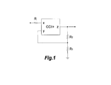
Inspection of the available current-conveyor based relaxation oscillators shows that a Schmitt trigger is required for each circuit implementation. While some implementations use current-in current-out Schmitt triggers others use the input-voltage output-voltage Schmitt trigger shown in FIG. 1 and described in Catalodo et al., (“A Schmitt trigger by means of a CCII+, International Journal of Circuit Theory and Applications, Vol. 23, 1995, pp. 161-165-incorporated herein by reference). Inspection of FIG. 1 shows that this Schmitt trigger circuit requires three resistors and does not have a low-output impedance terminal. Moreover, using this Schmitt trigger circuit a relaxation oscillator was proposed in Almashary et al., (“Current-mode triangular wave generator using CCIIs”, Microelectronics Journal, Vol. 31, 2000, pp. 239-243-incorporated herein by reference) with the resistance R replaced by the internal parasitic resistance rx of the second-generation current conveyor; as shown in FIG. 2. Thus, cascading the relaxation oscillator circuit, based on FIG. 1, for further signal processing, may require an impedance matching circuit.
Furthermore, the relaxation oscillator reported in Almashary et al., (“Current-mode triangular wave generator using CCIIs”, Microelectronics Journal, Vol. 31, 2000, pp. 239-243-incorporated herein by reference) was used as the basis for designing a current-conveyor based relaxation oscillator versatile electronic interface for capacitive and resistive sensors as described in Abuelma'atti et al., (“A current conveyor-based relaxation oscillator as a versatile electronic interface for capacitive and resistive sensors,” International Journal of Electronics, Vol. 92, 2005, pp. 473-477—incorporated herein by reference). In the interface circuit of the parasitic resistance rx is used for deciding the frequency of oscillation of the relaxation oscillator. While the resistance rx is relatively small its value is not constant. Thus, the operation of the electronic interface reported in Abuelma'atti et al., (“A current conveyor-based relaxation oscillator as a versatile electronic interface for capacitive and resistive sensors,” International Journal of Electronics, Vol. 92, 2005, pp. 473-477—incorporated herein by reference) may not be reliable.
SUMMARY
One embodiment of the disclosure includes a current-feedback operational-amplifier based serial resistive/serial capacitive/capacitive-resistive sensor electronic interfacing circuit system, including: a first output terminal; a serial resistive/serial capacitive/capacitive-resistive sensor having a first terminal and a second terminal; a reference capacitor directly coupled between the first terminal of the serial resistive/serial capacitive/capacitive-resistive sensor and a ground; a current-feedback operational-amplifier based Schmitt trigger circuit including: a first input terminal directly coupled to the second terminal of the serial resistive/serial capacitive/capacitive-resistive sensor; a second output terminal directly coupled to the first output terminal of the serial resistive/serial capacitive/capacitive-resistive sensor; a current feedback operational amplifier having a second input terminal, a third input terminal, a third output terminal and a fourth output terminal, wherein the third output terminal directly coupled to the first output terminal of the current-feedback operational-amplifier based serial resistive/serial capacitive/capacitive-resistive sensor electronic interfacing circuit system, and the fourth output terminal directly coupled to the third input terminal; a first resistor directly coupled between the first input terminal and the second input terminal, and a second resistor directly coupled between the third input terminal and a ground.
Another embodiment of the disclosure includes a current-feedback operational-amplifier based parallel capacitive sensor electronic interfacing circuit system, comprising: a first output terminal; a parallel capacitive sensor having a first terminal and a second terminal, wherein the second terminal directly coupled to a ground; a reference capacitor directly coupled between the first terminal of the parallel capacitive sensor and the ground; a current-feedback operational-amplifier based Schmitt trigger circuit including: a first input terminal directly coupled to the first terminal of the parallel capacitive sensor; a second output terminal, directly coupled to the first output terminal of the current-feedback operational-amplifier based parallel capacitive sensor electronic interfacing circuit system; a current feedback operational amplifier having a second input terminal, a third input terminal, a third output terminal and a fourth output terminal, wherein the third output terminal directly coupled to the first output terminal of the current-feedback operational-amplifier based parallel capacitive sensor electronic interfacing circuit system, and the fourth output terminal directly coupled to the third input terminal; a first resistor directly coupled between the first input terminal of the current-feedback operational-amplifier based Schmitt trigger circuit and the second input terminal, and a second resistor directly coupled between the third input terminal and a ground.
A further embodiment of the disclosure includes a current-feedback operational-amplifier based Schmitt trigger circuit including: a first input terminal; a first output terminal; a current feedback operational amplifier having a second input terminal, a third input terminal, a second output terminal and a third output terminal, wherein the second output terminal directly coupled to the first output terminal, and the third output terminal directly coupled to the third input terminal; a first resistor directly coupled between the first input terminal and the second input terminal; a second resistor directly coupled between the third input terminal and a ground.
BRIEF DESCRIPTION OF THE DRAWINGS
FIG. 1 is a schematic drawing of a CCII+ based Schmitt trigger circuit.
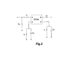
FIG. 2 is a schematic drawing of an AD844 current-feedback operational-amplifier.
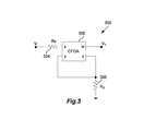
FIG. 3 is a schematic drawing of a proposed current-feedback operational-amplifier based Schmitt Trigger.
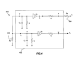
FIG. 4 is a schematic diagram of the proposed equivalent circuit of the current-feedback operational-amplifier based Schmitt Trigger.
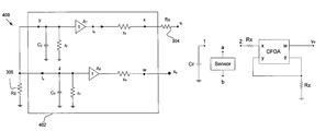
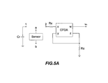
FIG. 5A is a schematic drawing of a proposed current-feedback operational-amplifier based capacitive/resistive sensor electronic interfacing circuit.
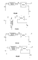
FIG. 5B is a schematic drawing of a proposed current-feedback operational-amplifier based serial resistive sensor electronic interfacing circuit.
FIG. 5C is a schematic drawing of a proposed current-feedback operational-amplifier based parallel capacitive sensor electronic interfacing circuit.
FIG. 5D is a schematic drawing of a proposed current-feedback operational-amplifier based serial capacitive sensor electronic interfacing circuit.
FIG. 5E is a schematic drawing of a proposed current-feedback operational-amplifier based serial capacitive-resistive sensor electronic interfacing circuit.
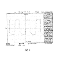
FIG. 6 is a plot of output waveform obtained from the FIG. 5A with RX=10.0K, RZ=1.0K and Cr=10.0 nF.
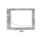
FIG. 7 is a plot of a variation of the output frequency of the circuit of FIG. 5A with the capacitance Rz at a condition that RX=1.0K and Cr=10.0 nF.
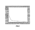
FIG. 8 is a plot of a variation of the output frequency of the circuit of FIG. 5A with the capacitance Cr at a condition that RZ=10.0K and RX=1.0K.
DETAILED DESCRIPTION OF THE PRESENT EMBODIMENTS
The present embodiment is a Current-Feedback Operational-Amplifier Based Relaxation Oscillator (CFOA)-based Schmitt trigger circuit that uses only two resistors and enjoys a low impedance output terminal. The use of the proposed Schmitt trigger circuit in designing a reliable electronic interface for capacitive, resistive or capacitive-resistive sensors is presented.
A current-feedback operational amplifier (CFOA) based relaxation oscillator 300, as shown in FIG. 3, includes a CFOA 302, an external resistor R X 304 connected between the CFOA x input and oscillator input Vi, and an external resistor R Z 306 connected between the y and z terminals of the CFOA 302 and ground. In FIG. 3, x and y are differential inputs to the CFOA 302, and w is the output pin. The equivalent circuit of this oscillator structure is shown in FIG. 4, wherein the dotted box represents a simplified equivalent circuit for the CFOA 302. In this equivalent circuit, rx and rw represent the output resistances of the unity-gain buffers A1 and A2, respectively; Cz is the internally connected compensation capacitor; Rz is the internal resistance of the gain node; and Cy and Ry represent the input impedance at terminal y of the CFOA.
In FIG. 3 the resistance RX is an externally connected resistance with RX>>rx where rX is the parasitic internal resistance at terminal x of the CFOA. The output of the Schmitt trigger of FIG. 3 will switch between its maximum, Vsat+, and minimum, Vsat−, when the input voltage, Vi, reaches the following two threshold voltages as described in equation (1) and (2):
Considering the circuit of FIG. 5 with nodes 1 and 2 connected and the sensor disconnected. Assume that the capacitor Cr has an initial voltage=Vth−, and is charging through the resistance RX heading towards Vsat+. The voltage across the capacitor can be described as:
V C r (t)=V sat+−(V sat+ −V th−)exp(−t/C r R X) (3)
The capacitor will continue charging until its voltage reaches Vth+ when the output voltage of the CFOA switches to Vsat− and the process will be reversed. Using equation (3), the time T1 required to charge the capacitor from Vth− to Vth+ will be given by:
When the capacitor voltage reaches Vth+ the output voltage of the CFOA switches to Vsat− and the capacitor starts a charging process heading towards Vsat−. The voltage across the capacitor can be described as:
V C r (t)=V sat−−(V sat− −V th+)exp(−t/C r R X) (5)
The capacitor will continue charging until its voltage reaches Vth− when the output voltage of the CFOA switches to Vsat+ and the process will be reversed. Using equation (5), the time T2 required to charge the capacitor from Vth+ to Vth− will be given by:
When the voltage across the capacitor reaches Vth− the output voltage of the CFOA switches to Vsat+ and the process will be repeated. Using equations (4) and (6) the duration of the resulting oscillation period will be given by
Inspection of equations (1), (2), (4) and (6) clearly shows that a square-wave with duty cycle different from 50% can be obtained by proper selection of Vsat+ and Vsat−.
Combining equations (1), (2) and (7) yields
For the special case with Vsat−=Vsat+ equation (8) reduces to
In the proposed CFOA-based capacitive/resistive sensor electronic interfacing circuit shown in FIG. 5A the dotted box can be:
For case (a), as shown in FIG. 5B, a resistive sensor with resistance Rs connected in series with the reference capacitance Cr; that is with terminal a connected to terminal 1 and terminal b connected to terminal 2. In this case the resistance RX in equations (8) and (9) will be replaced by RST=Rs+RX, and the oscillation period of serial resistive sensor network can be described as:
For the special case with Vsat−=−Vsat+ equation (10) reduces to
For case (b), as shown in FIG. 5C, a capacitive sensor with capacitance Cs connected in parallel with the reference capacitor Cr; that is with terminal a connected to terminal 1 and terminal 2 and terminal b connected to the ground. In this case the capacitance Cr in equations (8) and (9) will be replaced by CPT=Cr+Cs and the oscillation period of parallel capacitive sensor network is described as:
For the special case with Vsat−=−Vsat+ equation (12) reduces to
For case (c), as shown in FIG. 5D, a capacitive sensor with capacitance Cs connected in series with the reference capacitor Cr; that is with terminal a connected to terminal 1 and terminal b connected to terminal 2. In this case the capacitance Cr in equations (8) and (9) will be replaced by CST≅CrCs/(Cr+Cs) and the oscillation period of serial capacitive sensor network is described as:
For the special case with Vsat−=−Vsat+ equation (14) reduces to
For case (d), as shown in FIG. 5E, a capacitive-resistive sensor with capacitance Cs and resistance connected Rs in series with the reference capacitor Cr; that is with terminal a connected to terminal 1 and terminal b connected to terminal 2. In this case the capacitance Cr and the resistance RX in equations (8) and (9) will be replaced by CT≅CrCs/(Cr+Cs) and RT≅RX+RS respectively, and the oscillation period of capacitive-resistive sensor network is described as:
For the special case with Vsat−=−Vsat+ equation (16) reduces to
The approximations made in cases (a) and (d) are based on the assumptions that the time constant Cxrx<<CTRs.
The proposed circuit of FIG. 5A was tested using the current-feedback operational-amplifier AD844 (Spice model available from Analog Device is shown in FIG. 2 using the following values of the components: Rz≅3, MΩ, CZ≅4.5 pF, Ry≅10 MΩ, Cy≈2.0 pF, and rx≈50Ω). By selecting Cr=10 nF and Rx=10 kΩ, then RZ=1.0K, rectangular oscillations are obtained, as shown in plot of FIG. 6. The variations of the frequency of oscillation with the capacitance Cr and the resistance RZ are shown in FIGS. 7 and 8. These results are obtained with DC supply voltage=±10V.