WO2014181890A2 - 有機螺旋構造体の製造方法、及びそれにより製造される有機螺旋構造体 - Google Patents
有機螺旋構造体の製造方法、及びそれにより製造される有機螺旋構造体 Download PDFInfo
- Publication number
- WO2014181890A2 WO2014181890A2 PCT/JP2014/062634 JP2014062634W WO2014181890A2 WO 2014181890 A2 WO2014181890 A2 WO 2014181890A2 JP 2014062634 W JP2014062634 W JP 2014062634W WO 2014181890 A2 WO2014181890 A2 WO 2014181890A2
- Authority
- WO
- WIPO (PCT)
- Prior art keywords
- polymer
- helical structure
- optical vortex
- organic
- optical
- Prior art date
Links
Images

Classifications
-
- C—CHEMISTRY; METALLURGY
- C08—ORGANIC MACROMOLECULAR COMPOUNDS; THEIR PREPARATION OR CHEMICAL WORKING-UP; COMPOSITIONS BASED THEREON
- C08J—WORKING-UP; GENERAL PROCESSES OF COMPOUNDING; AFTER-TREATMENT NOT COVERED BY SUBCLASSES C08B, C08C, C08F, C08G or C08H
- C08J7/00—Chemical treatment or coating of shaped articles made of macromolecular substances
-
- B—PERFORMING OPERATIONS; TRANSPORTING
- B82—NANOTECHNOLOGY
- B82Y—SPECIFIC USES OR APPLICATIONS OF NANOSTRUCTURES; MEASUREMENT OR ANALYSIS OF NANOSTRUCTURES; MANUFACTURE OR TREATMENT OF NANOSTRUCTURES
- B82Y30/00—Nanotechnology for materials or surface science, e.g. nanocomposites
-
- B—PERFORMING OPERATIONS; TRANSPORTING
- B82—NANOTECHNOLOGY
- B82Y—SPECIFIC USES OR APPLICATIONS OF NANOSTRUCTURES; MEASUREMENT OR ANALYSIS OF NANOSTRUCTURES; MANUFACTURE OR TREATMENT OF NANOSTRUCTURES
- B82Y40/00—Manufacture or treatment of nanostructures
-
- C—CHEMISTRY; METALLURGY
- C08—ORGANIC MACROMOLECULAR COMPOUNDS; THEIR PREPARATION OR CHEMICAL WORKING-UP; COMPOSITIONS BASED THEREON
- C08G—MACROMOLECULAR COMPOUNDS OBTAINED OTHERWISE THAN BY REACTIONS ONLY INVOLVING UNSATURATED CARBON-TO-CARBON BONDS
- C08G73/00—Macromolecular compounds obtained by reactions forming a linkage containing nitrogen with or without oxygen or carbon in the main chain of the macromolecule, not provided for in groups C08G12/00 - C08G71/00
- C08G73/02—Polyamines
-
- G—PHYSICS
- G02—OPTICS
- G02B—OPTICAL ELEMENTS, SYSTEMS OR APPARATUS
- G02B21/00—Microscopes
- G02B21/0096—Microscopes with photometer devices
-
- G—PHYSICS
- G02—OPTICS
- G02B—OPTICAL ELEMENTS, SYSTEMS OR APPARATUS
- G02B27/00—Optical systems or apparatus not provided for by any of the groups G02B1/00 - G02B26/00, G02B30/00
- G02B27/28—Optical systems or apparatus not provided for by any of the groups G02B1/00 - G02B26/00, G02B30/00 for polarising
- G02B27/286—Optical systems or apparatus not provided for by any of the groups G02B1/00 - G02B26/00, G02B30/00 for polarising for controlling or changing the state of polarisation, e.g. transforming one polarisation state into another
-
- G—PHYSICS
- G02—OPTICS
- G02B—OPTICAL ELEMENTS, SYSTEMS OR APPARATUS
- G02B5/00—Optical elements other than lenses
- G02B5/30—Polarising elements
- G02B5/3025—Polarisers, i.e. arrangements capable of producing a definite output polarisation state from an unpolarised input state
- G02B5/3033—Polarisers, i.e. arrangements capable of producing a definite output polarisation state from an unpolarised input state in the form of a thin sheet or foil, e.g. Polaroid
-
- G—PHYSICS
- G02—OPTICS
- G02B—OPTICAL ELEMENTS, SYSTEMS OR APPARATUS
- G02B5/00—Optical elements other than lenses
- G02B5/30—Polarising elements
- G02B5/3083—Birefringent or phase retarding elements
Definitions
- the present invention relates to an organic spiral structure and a method for producing the same.
- An optical vortex is a light wave having the characteristic properties of angular momentum (orbital angular momentum) derived from phase singularities and donut-type intensity distribution.
- a Laguerre Gaussian beam can be cited (for example, see Non-Patent Document 1 below).
- the wavefront of the optical vortex has a helical shape, and the orbital angular momentum acts in the direction given by the vector difference between the normal direction and the light propagation direction.
- optical vortices can be used for optical manipulation using the radiation pressure of light, high-resolution microscopes using phase singularities, optical vortex ablation processing that actively uses orbital angular momentum, etc. Use is expected greatly.
- Patent Document 1 As a known technique for oscillating an optical vortex, for example, an apparatus described in Patent Document 1 below can be exemplified.
- Patent Document 1 and Non-Patent Document 1 are techniques that focus on the optical vortex oscillation method itself, and the applications using the optical vortex including the optical manipulations listed above are not being studied. There remains room.
- the present invention aims to provide a possibility of new application of the optical vortex.
- the present inventors have been diligently studying the above problem, and found that when an azo polymer exhibiting a photoisomerization reaction is irradiated with a light vortex, a nanoscale helical structure is formed on the polymer surface.
- the present invention has been completed.
- a nanoscale helical structure is formed on the surface of the polymer by irradiating the surface of the polymer exhibiting a photoisomerization reaction with a light vortex. It is characterized by that.
- the polymer exhibiting a photoisomerization reaction is preferably at least one of an azo polymer and a spiropyran polymer.
- nanoscale helical structure it is preferable to repeat the step of forming a nanoscale helical structure to form a plurality of nanoscale helical structures two-dimensionally on the surface of the polymer.
- the organic helical structure according to another aspect of the present invention has a nanoscale helical structure formed on the surface of a polymer exhibiting a photoisomerization reaction.
- the present invention can provide the possibility of new application of the optical vortex.
- a plurality of helical structures provided by the present invention can be arranged two-dimensionally at the nano level, thereby enabling metamaterials, bio-MEMS, circular dichroism exhibiting optical rotation in the terahertz wave region. Applications in various fields such as issuing and absorbing elements and organic solar cells can be expected.
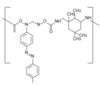
- FIG. 3 is a diagram showing a chemical formula of Poly-Orange Tom-1. It is an AFM image which shows the state of the surface of an organic helical structure.
- the method for producing an organic helical structure according to the present embodiment is characterized in that a nano-scale helical structure is formed on the surface of the polymer by irradiating the surface of the polymer exhibiting a photoisomerization reaction with an optical vortex. To do.
- optical vortex refers to a light wave having the characteristic properties of angular momentum (orbital angular momentum) derived from phase singularities and donut-shaped intensity distribution as described above.
- the method for generating the optical vortex is not limited, but for example, an optical vortex laser oscillation device (hereinafter referred to as “the present laser device”) as shown in FIG. 1 can be used.
- the present laser device an optical vortex laser oscillation device
- FIG. 1 is a diagram showing an outline of an optical system of an optical vortex laser oscillation apparatus (hereinafter referred to as “the present laser apparatus”) 1 according to the present embodiment.
- the laser device 1 includes a laser light source 2 that emits a laser beam B1, an optical vortex generator 3 that generates an optical vortex B2 based on the laser beam B1 that the laser light source 2 emits, and an optical vortex generator 3
- the quarter wave plate 4 which makes the optical vortex B2 which generate
- the laser light source 2 can emit the laser beam B1 as described above.
- the laser light source 2 is not limited as long as it has the above function, and a solid laser such as a YAG laser, a gas laser such as a dye laser and a He—Ne laser, a semiconductor laser such as an LD laser, and the like can be used. However, it is not limited to this.
- the wavelength range of the light emitted from the laser light source 2 in the present embodiment is preferably a wavelength range in which the irradiation target can cause a photoisomerization reaction. This wavelength range can be appropriately adjusted depending on the material, but it is preferably in the ultraviolet region to the near infrared region, and more specifically in the range of 350 nm to 1 ⁇ m.
- the laser light source 2 is preferably a continuous wave laser light source that emits continuous wave laser light.
- a continuous wave laser beam By using a continuous wave laser beam, it is possible to continuously irradiate a polymer with an optical vortex.
- the repetition frequency is sufficiently high so that the photoisomerization reaction can be maintained.
- the optical vortex generator 3 can emit the optical vortex B2 based on the laser beam B1 emitted from the laser light source 2, and is not limited to this, but for example, a phase plate, spatial phase modulation, etc.
- a multimode area fiber amplifier or the like can be used.
- the laser light source 2 and the optical vortex generator 3 may be integrated to generate an optical vortex directly.
- the optical vortex generated in the optical vortex generator is particularly preferably a coherent optical vortex.
- the quarter wavelength plate 4 is used to change the optical vortex into circularly polarized light B3. If the optical vortex generator 3 is already circularly polarized, it can be omitted. In the present embodiment, by providing a quarter-wave plate, a helical structure can be generated on the surface of a polymer that exhibits a photoisomerization reaction.
- the light condensing unit 5 is used for condensing light and efficiently irradiating the surface of the polymer 7 exhibiting a photoisomerization reaction.
- the structure of the light collecting unit 5 is not limited as long as it can efficiently irradiate the circularly polarized light vortex, but for example, it is preferably configured to include a microscope objective lens. .
- the beam diameter can be adjusted to a desired diameter with the microscope objective lens.
- an observation unit 6 may be provided for observing the surface of a polymer that exhibits a photoisomerization reaction.
- the observation unit 6 is not limited as long as it has the above function.
- the observation unit 6 divides the optical vortex collected by the light collection unit 5 and performs one of the light division members 61 and photoisomerization.
- an imaging member 62 for observing light reflected from the surface of the polymer exhibiting a reaction. Examples of the imaging member 62 include, but are not limited to, a CCD camera and the like, and it is preferable to connect an information processing device such as a so-called personal computer to perform image processing.
- a polymer exhibiting a photoisomerization reaction irradiated with a photovortex can cause an isomerization reaction that becomes one of two types of structural isomers when irradiated with a photovortex.
- a polymer. Examples of the polymer exhibiting a photoisomerization reaction are not limited as long as they have the above-described function, but are preferably at least one of an azo polymer and a spiropyran polymer.
- the “azo polymer” refers to a polymer containing an azo group in a unit constituting the polymer and having a structural isomer such as a cis type or a trans type.
- Specific examples of the compound containing an azo group include azobenzene and a derivative in which a substituent is attached to carbon in the azobenzene, and the like is not limited as long as it shows a photoisomerization reaction. .
- the “spiropyran polymer” is a polymer containing a structure (spiropyran) in which two pyran rings are spiro-bonded in units constituting the polymer, and the spiro ring has a cyclic structure. That which can take two or more states of the state which has become a ring-opening structure.
- Specific examples of the spiropyran-based polymer are not limited, but spirobenzopyran and derivatives having a substituent added thereto can be exemplified as long as they exhibit a photoisomerization reaction. It is not limited.
- a rhodopsin-based polymer may be used.
- “Rhodopsin-based polymer” refers to a polymer contained in the units constituting rhodopsin. Since the structure of rhodopsin also changes due to light irradiation, a helical structure can be produced at the nano level.
- the energy of the optical vortex irradiated in the present embodiment is too small, the spiral structure cannot be formed, and if it is too high, the polymer is decomposed. However, it is preferably in the range of 1 ⁇ W to 1 mW.
- a nanoscale helical structure can be formed on the surface of the polymer by irradiating the surface of the polymer exhibiting a photoisomerization reaction with a photovortex.
- the main mechanism by which the helical structure is formed is mass transfer by photoisomerization reaction.
- a metal is irradiated with an optical vortex
- a spiral needle can be formed on the surface of the metal, but it is mainly a physical phenomenon such as melting and transpiration of the metal that occurs predominantly in the dynamics in which the spiral needle is formed, Although the final result that the spiral structure is formed by the light vortex irradiation looks the same, it is a completely different phenomenon.
- there is no precedent for forming a nanoscale helical structure on the surface of an azo polymer thin film by light irradiation and this is the first report in the world.
- a dynamic spatial movement of the molecule occurs through the photoisomerization reaction.
- an example of an azo polymer azobenzene
- azobenzene which is a trans form
- isomerization to a cis form occurs. Since the cis isomer has a larger volume than the trans isomer, the intermolecular distance increases and the intermolecular force decreases.
- the trans-cis isomerization reaction is a reversible reaction, and when the light irradiation is stopped, isomerization immediately occurs from the cis form to the trans form, so that the polymer surface solidifies again and a relief is formed on the surface.
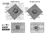
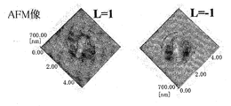
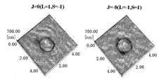
- FIG. 2 shows an AFM image and a laser scanning microscope image of the spiral structure when the total angular momentum, orbital angular momentum, and spin angular momentum are changed.
- FIG. 3 shows an AFM image in this case.
- the chirality of the spiral structure can be reliably determined. There is an effect that can be.
- this operation can be performed in an extremely short time, and there is an advantage that it can be formed with an overwhelmingly high yield and a short working time compared to other chemical processes.
- the step of forming the nanoscale spiral structure it is preferable to repeat the step of forming the nanoscale spiral structure to form a plurality of nanoscale spiral structures two-dimensionally on the surface of the polymer.
- the present invention can provide the possibility of new application of the optical vortex.
- the helical structure provided by the present invention can be easily arranged in a nano-level and two-dimensionally in just a few seconds, and thus a metamaterial that exhibits optical rotation in the terahertz wave region, bio-MEMS Application in various fields such as circular dichroism issuance and absorption elements, organic solar cells can be expected.
- a CW laser having a center wavelength of 532 nm is used through a helical phase plate (SPP), a ⁇ / 4 plate (QWP), and an objective lens (NA to 0.44).
- Azopolymer was irradiated.
- the diameter of the laser spot irradiated on the azopolymer was 3 ⁇ m.
- the azo polymer used was Poly-Orange Tom-1 (hereinafter referred to as “POT”; see FIG. 4 for the structure).
- the POT concentration was 16.6 wt% (cyclohexane solvent), the spin coating conditions were 2500 rpm for 10 sec, and 4000 rpm for 60 sec.
- a thin film was formed by applying POT on a glass substrate.
- the size can be changed for irradiation.
- 2
- the present invention has an industrial applicability as a method for producing an organic helical structure, and an organic helical structure produced thereby.
- the organic helical structure is a metamaterial that exhibits optical activity in the terahertz wave region, bio Applications in various fields such as MEMS, circular dichroism issuance and absorption elements, and organic solar cells can be expected.
Abstract
Description
Claims (6)
- 光渦を、光異性化反応を示す高分子の表面に照射して、前記高分子の表面にナノスケールの螺旋構造を形成する、有機螺旋構造体の製造方法。
- 前記光異性化反応を示す高分子は、アゾ系ポリマー及びスピロピラン系ポリマーの少なくともいずれかである請求項1記載の有機螺旋構造体の製造方法。
- 前記ナノスケールの螺旋構造を形成するステップを繰り返し、前記ナノスケールの螺旋構造を、前記高分子の表面に二次元的に複数形成する、請求項1記載の有機螺旋構造体の製造方法。
- 前記光渦は、円偏光である請求項1記載の有機螺旋構造体の製造方法。
- 前記光渦の全角運動量Jは0でない請求項1記載の有機螺旋構造体の製造方法。
- 光異性化反応を示す高分子の表面に、ナノスケールの螺旋構造が形成された有機螺旋構造体。
Priority Applications (2)
| Application Number | Priority Date | Filing Date | Title |
|---|---|---|---|
| US14/890,161 US10099921B2 (en) | 2013-05-10 | 2014-05-12 | Method for producing organic helical structure, and organic helical structure produced using said method |
| JP2015515918A JP6363069B2 (ja) | 2013-05-10 | 2014-05-12 | 有機螺旋構造体の製造方法、及びそれにより製造される有機螺旋構造体 |
Applications Claiming Priority (2)
| Application Number | Priority Date | Filing Date | Title |
|---|---|---|---|
| JP2013100784 | 2013-05-10 | ||
| JP2013-100784 | 2013-05-10 |
Publications (2)
| Publication Number | Publication Date |
|---|---|
| WO2014181890A2 true WO2014181890A2 (ja) | 2014-11-13 |
| WO2014181890A3 WO2014181890A3 (ja) | 2014-12-31 |
Family
ID=51867828
Family Applications (1)
| Application Number | Title | Priority Date | Filing Date |
|---|---|---|---|
| PCT/JP2014/062634 WO2014181890A2 (ja) | 2013-05-10 | 2014-05-12 | 有機螺旋構造体の製造方法、及びそれにより製造される有機螺旋構造体 |
Country Status (3)
| Country | Link |
|---|---|
| US (1) | US10099921B2 (ja) |
| JP (1) | JP6363069B2 (ja) |
| WO (1) | WO2014181890A2 (ja) |
Cited By (4)
| Publication number | Priority date | Publication date | Assignee | Title |
|---|---|---|---|---|
| JPWO2016136722A1 (ja) * | 2015-02-25 | 2018-01-11 | 株式会社リコー | 光吸収材飛翔装置及び光吸収材飛翔方法、並びに、それを用いた応用 |
| JP2018040101A (ja) * | 2016-08-31 | 2018-03-15 | 国立大学法人千葉大学 | キラルマイクロファイバーの製造方法及びこれにより製造されるキラルマイクロファイバー |
| CN108025577A (zh) * | 2015-10-06 | 2018-05-11 | 株式会社理光 | 图像形成方法、图像形成设备、激光照射印刷墨和用于制造图像形成物体的方法 |
| CN109310853A (zh) * | 2016-05-09 | 2019-02-05 | 新信心股份有限公司 | 激光加工方法以及微针的制造方法 |
Families Citing this family (4)
| Publication number | Priority date | Publication date | Assignee | Title |
|---|---|---|---|---|
| CN109154746A (zh) * | 2016-05-20 | 2019-01-04 | 夏普株式会社 | 液晶显示面板及液晶显示装置 |
| TWI651906B (zh) * | 2018-06-08 | 2019-02-21 | 國立中山大學 | 螺旋相位調制共振腔渦旋雷射光產生器及渦旋雷射光的產生方法 |
| US20230408635A1 (en) * | 2018-07-16 | 2023-12-21 | Or-Ment Llc | Electromagnetic wave medical imaging system, device and methods |
| CN110320672B (zh) * | 2019-07-08 | 2022-05-17 | 南京晶萃光学科技有限公司 | 一种太赫兹涡旋光产生器、制备方法及产生系统 |
Family Cites Families (5)
| Publication number | Priority date | Publication date | Assignee | Title |
|---|---|---|---|---|
| JP2003039400A (ja) * | 2001-08-03 | 2003-02-13 | Toyota Central Res & Dev Lab Inc | 微細光加工方法、微細光加工品及び光記録媒体 |
| JP2004294544A (ja) | 2003-03-25 | 2004-10-21 | Japan Science & Technology Agency | 光学材料の光誘起表面レリーフ形成を用いた光集積導波路素子 |
| WO2005088409A1 (ja) | 2004-03-12 | 2005-09-22 | Japan Science And Technology Agency | 光導波路型ホログラフィックメモリ |
| JP5531261B2 (ja) * | 2009-03-27 | 2014-06-25 | 国立大学法人 千葉大学 | レーザー加工方法、円偏光光渦レーザービームを用いたレーザー加工方法、針状体を有する部材の製造方法、および針状体を有する部材 |
| JP6103597B2 (ja) | 2011-06-07 | 2017-03-29 | 国立大学法人 千葉大学 | 光渦レーザー発振方法及び光渦レーザー発振装置 |
-
2014
- 2014-05-12 US US14/890,161 patent/US10099921B2/en active Active
- 2014-05-12 JP JP2015515918A patent/JP6363069B2/ja active Active
- 2014-05-12 WO PCT/JP2014/062634 patent/WO2014181890A2/ja active Application Filing
Cited By (10)
| Publication number | Priority date | Publication date | Assignee | Title |
|---|---|---|---|---|
| JPWO2016136722A1 (ja) * | 2015-02-25 | 2018-01-11 | 株式会社リコー | 光吸収材飛翔装置及び光吸収材飛翔方法、並びに、それを用いた応用 |
| CN107635779A (zh) * | 2015-02-25 | 2018-01-26 | 株式会社理光 | 光吸收材料喷射装置、光吸收材料喷射方法和使用其的应用 |
| EP3263339A4 (en) * | 2015-02-25 | 2018-04-18 | Ricoh Company, Ltd. | Light-absorbing material jetting device, light-absorbing material jetting method, and applications using same |
| US10427322B2 (en) | 2015-02-25 | 2019-10-01 | Ricoh Company, Ltd. | Light-absorbing material flying apparatus, method for flying light-absorbing material, and applications using same |
| CN107635779B (zh) * | 2015-02-25 | 2019-12-13 | 株式会社理光 | 光吸收材料喷射装置、光吸收材料喷射方法和使用其的应用 |
| CN108025577A (zh) * | 2015-10-06 | 2018-05-11 | 株式会社理光 | 图像形成方法、图像形成设备、激光照射印刷墨和用于制造图像形成物体的方法 |
| US10603925B2 (en) | 2015-10-06 | 2020-03-31 | Ricoh Company, Ltd. | Image-forming method, image-forming apparatus, laser irradiation printing ink, and method for manufacturing object with formed image |
| CN109310853A (zh) * | 2016-05-09 | 2019-02-05 | 新信心股份有限公司 | 激光加工方法以及微针的制造方法 |
| JPWO2017195790A1 (ja) * | 2016-05-09 | 2019-04-18 | シンクランド株式会社 | レーザ加工方法及びマイクロニードルの製造方法 |
| JP2018040101A (ja) * | 2016-08-31 | 2018-03-15 | 国立大学法人千葉大学 | キラルマイクロファイバーの製造方法及びこれにより製造されるキラルマイクロファイバー |
Also Published As
| Publication number | Publication date |
|---|---|
| WO2014181890A3 (ja) | 2014-12-31 |
| US10099921B2 (en) | 2018-10-16 |
| JP6363069B2 (ja) | 2018-07-25 |
| US20160107888A1 (en) | 2016-04-21 |
| JPWO2014181890A1 (ja) | 2017-02-23 |
Similar Documents
| Publication | Publication Date | Title |
|---|---|---|
| JP6363069B2 (ja) | 有機螺旋構造体の製造方法、及びそれにより製造される有機螺旋構造体 | |
| Wang et al. | Two‐photon polymerization lithography for optics and photonics: fundamentals, materials, technologies, and applications | |
| Hu et al. | Laser-splashed three-dimensional plasmonic nanovolcanoes for steganography in angular anisotropy | |
| Rekstyte et al. | Nanoscale precision of 3D polymerisation via polarisation control | |
| Toyoda et al. | Using optical vortex to control the chirality of twisted metal nanostructures | |
| Hu et al. | Bio-inspired hierarchical patterning of silicon by laser interference lithography | |
| JP6498804B2 (ja) | アミノ酸結晶の製造方法 | |
| Shakhov et al. | Femtosecond nanostructuring of glass with optically trapped microspheres and chemical etching | |
| Wang et al. | Nanoscale material redistribution induced by spatially modulated femtosecond laser pulses for flexible high-efficiency surface patterning | |
| Lin et al. | Microsphere femtosecond laser sub-50 nm structuring in far field via non-linear absorption | |
| Quentin et al. | Optical trap assisted laser nanostructuring in the near-field of microparticles | |
| JOCHCOVA et al. | INTENSITY DISTRIBUTION MODULATION OF MULTIPLE BEAM INTERFERENCE PATTERN. | |
| Kim et al. | Coherent Manipulation of Extreme-Ultraviolet Bessel Vortex Beams from Solids by Active Wavefront Shaping of Driving Fundamental Beams | |
| Beresna et al. | Harnessing Ultrafast Laser Induced Nanostructures in Transparent Materials | |
| Drampyan et al. | Optical micro-structuring of metal films on the surface of dielectric materials: prospects of shaping by non-diffracting optical beams | |
| Astafiev et al. | Microstructuring of polymer films by femtosecond pulses through optically trapped polystyrene microspheres | |
| RU196429U1 (ru) | Устройство формирования пучка Эйри | |
| RU196430U1 (ru) | Устройство формирования пучка Эйри в терагерцовом диапазоне длин волн | |
| Badalyan et al. | Talbot effect from periodic and quasi-periodic structures: application to 3D quasi-crystalline photonic lattices formation | |
| Tsai et al. | Laser direct-write nanopatterning by near-field multiphoton polymerization using optically trapped microspheres | |
| JP6982817B2 (ja) | キラルマイクロファイバーの製造方法及びこれにより製造されるキラルマイクロファイバー | |
| Chung | Controlling motion at the nanoscale with light | |
| Lu et al. | New Methods of Laser Micro-Nanomanufacturing | |
| Porfirev et al. | Structured polarized laser beams for controlled spiral-shaped mass transfer in | |
| Kostyuk et al. | Birefringent phase masks for laser beams shaping during laser material processing at imaging plane |
Legal Events
| Date | Code | Title | Description |
|---|---|---|---|
| 121 | Ep: the epo has been informed by wipo that ep was designated in this application |
Ref document number: 14794127 Country of ref document: EP Kind code of ref document: A2 |
|
| ENP | Entry into the national phase |
Ref document number: 2015515918 Country of ref document: JP Kind code of ref document: A |
|
| WWE | Wipo information: entry into national phase |
Ref document number: 14890161 Country of ref document: US |
|
| 122 | Ep: pct application non-entry in european phase |
Ref document number: 14794127 Country of ref document: EP Kind code of ref document: A2 |