WO2014181770A1 - 発光パターンを有する有機エレクトロルミネッセンス素子の製造方法 - Google Patents
発光パターンを有する有機エレクトロルミネッセンス素子の製造方法 Download PDFInfo
- Publication number
- WO2014181770A1 WO2014181770A1 PCT/JP2014/062155 JP2014062155W WO2014181770A1 WO 2014181770 A1 WO2014181770 A1 WO 2014181770A1 JP 2014062155 W JP2014062155 W JP 2014062155W WO 2014181770 A1 WO2014181770 A1 WO 2014181770A1
- Authority
- WO
- WIPO (PCT)
- Prior art keywords
- light
- layer
- organic
- light emission
- electrode
- Prior art date
- Legal status (The legal status is an assumption and is not a legal conclusion. Google has not performed a legal analysis and makes no representation as to the accuracy of the status listed.)
- Ceased
Links
Images

Classifications
-
- H—ELECTRICITY
- H10—SEMICONDUCTOR DEVICES; ELECTRIC SOLID-STATE DEVICES NOT OTHERWISE PROVIDED FOR
- H10K—ORGANIC ELECTRIC SOLID-STATE DEVICES
- H10K71/00—Manufacture or treatment specially adapted for the organic devices covered by this subclass
- H10K71/20—Changing the shape of the active layer in the devices, e.g. patterning
-
- H—ELECTRICITY
- H10—SEMICONDUCTOR DEVICES; ELECTRIC SOLID-STATE DEVICES NOT OTHERWISE PROVIDED FOR
- H10K—ORGANIC ELECTRIC SOLID-STATE DEVICES
- H10K71/00—Manufacture or treatment specially adapted for the organic devices covered by this subclass
-
- H—ELECTRICITY
- H10—SEMICONDUCTOR DEVICES; ELECTRIC SOLID-STATE DEVICES NOT OTHERWISE PROVIDED FOR
- H10K—ORGANIC ELECTRIC SOLID-STATE DEVICES
- H10K71/00—Manufacture or treatment specially adapted for the organic devices covered by this subclass
- H10K71/40—Thermal treatment, e.g. annealing in the presence of a solvent vapour
-
- H—ELECTRICITY
- H10—SEMICONDUCTOR DEVICES; ELECTRIC SOLID-STATE DEVICES NOT OTHERWISE PROVIDED FOR
- H10K—ORGANIC ELECTRIC SOLID-STATE DEVICES
- H10K85/00—Organic materials used in the body or electrodes of devices covered by this subclass
- H10K85/30—Coordination compounds
- H10K85/321—Metal complexes comprising a group IIIA element, e.g. Tris (8-hydroxyquinoline) gallium [Gaq3]
- H10K85/324—Metal complexes comprising a group IIIA element, e.g. Tris (8-hydroxyquinoline) gallium [Gaq3] comprising aluminium, e.g. Alq3
-
- H—ELECTRICITY
- H10—SEMICONDUCTOR DEVICES; ELECTRIC SOLID-STATE DEVICES NOT OTHERWISE PROVIDED FOR
- H10K—ORGANIC ELECTRIC SOLID-STATE DEVICES
- H10K85/00—Organic materials used in the body or electrodes of devices covered by this subclass
- H10K85/30—Coordination compounds
- H10K85/341—Transition metal complexes, e.g. Ru(II)polypyridine complexes
- H10K85/342—Transition metal complexes, e.g. Ru(II)polypyridine complexes comprising iridium
-
- H—ELECTRICITY
- H10—SEMICONDUCTOR DEVICES; ELECTRIC SOLID-STATE DEVICES NOT OTHERWISE PROVIDED FOR
- H10K—ORGANIC ELECTRIC SOLID-STATE DEVICES
- H10K85/00—Organic materials used in the body or electrodes of devices covered by this subclass
- H10K85/60—Organic compounds having low molecular weight
- H10K85/649—Aromatic compounds comprising a hetero atom
- H10K85/657—Polycyclic condensed heteroaromatic hydrocarbons
- H10K85/6572—Polycyclic condensed heteroaromatic hydrocarbons comprising only nitrogen in the heteroaromatic polycondensed ring system, e.g. phenanthroline or carbazole
Definitions
- the present invention relates to a method for manufacturing an organic electroluminescence element having a light emission pattern with excellent gradation characteristics.
- organic light emitting devices are attracting attention as thin light emitting materials.
- Organic light-emitting elements (hereinafter also referred to as “organic EL elements”) using organic electroluminescence (EL) are thin-film type solid solids capable of emitting light at a low voltage of several V to several tens V. It is an element and has many excellent features such as high brightness, high luminous efficiency, thinness, and light weight. For this reason, it has been attracting attention in recent years as surface light emitters such as backlights for various displays, display boards such as signboards and emergency lights, and illumination light sources.
- Such an organic EL element has a configuration in which a light emitting layer made of an organic material is disposed between two electrodes, and emitted light generated in the light emitting layer passes through the electrode and is extracted outside. For this reason, at least one of the two electrodes is configured as a transparent electrode, and emitted light is extracted from the transparent electrode side.
- the organic EL element can obtain high luminance with low power, and is excellent in terms of visibility, response speed, life, and power consumption.
- an organic EL element having a light-emitting pattern that forms a non-light-emitting region by irradiating the organic functional layer laminated on the glass substrate with ultraviolet rays and deteriorating the irradiated portion.
- Patent Document 1 and Patent Document 2 See, for example, Patent Document 1 and Patent Document 2.
- the present invention has been made in view of the above problems and situations, and a problem to be solved is to provide a method for producing an organic electroluminescent element having a light emission pattern with excellent gradation characteristics.
- the inventors of the present invention in the course of studying the cause of the above problems, the gradation characteristics of the light emission pattern of the organic electroluminescence element having the light emission pattern are the gradation of the highlight part and the shadow part.
- the present inventors have found that the range of reproduction is narrow and the image is unnatural, leading to the present invention.
- a method for producing an organic electroluminescent element having a light emission pattern formed by irradiating light to an organic electroluminescent element having one or a plurality of organic functional layers between at least a pair of electrodes For the image to be patterned, it is a tone reproduction curve that is created in advance and consists of a highlight part, a shadow part, and a straight part, and has a soft part that is lower than the gradient of the gradation of the straight part in the highlight part and the shadow part.
- a method for producing an organic electroluminescence element having a light emission pattern wherein the light emission amount is changed to form a light emission pattern having a gradation with light emission luminance corresponding to the light irradiation amount.
- the value of the ratio of the maximum light emission luminance and the minimum luminance of the organic electroluminescence element having the light emission pattern is 10 or more, The organic electroluminescence element having the light emission pattern according to item 1 or 2, Production method.
- the soft portion of the highlight portion in the tone reproduction curve is in the range of at least ⁇ 0.20 in terms of a common logarithm (log (light emission luminance)) of light emission luminance from the maximum light emission luminance of the organic electroluminescence element having a light emission pattern.
- the soft portion of the shadow portion is within the range of at least +0.20 in terms of the common logarithm (log (emission luminance)) of the emission luminance from the lowest luminance of the organic electroluminescence element having the light pattern.
- the organic electroluminescence element according to any one of items 1 to 4, wherein the light emission pattern formed by light irradiation is a light emission pattern formed by irradiation with light including ultraviolet rays. Manufacturing method.
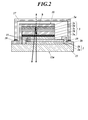
- An example of a tone reproduction curve that has a soft part lower than the gradient of the gradation of the straight part in the highlight part and shadow part An example of a sectional view showing a schematic configuration of an organic EL element
- the method for producing an organic electroluminescent element having a light emitting pattern comprises an organic electroluminescent element having a light emitting pattern formed by irradiating an organic electroluminescent element having one or more organic functional layers between at least a pair of electrodes.
- a method of manufacturing a luminescence element which is made of a highlight portion, a shadow portion, and a straight portion, and is lower than the gradient of gradation of the straight portion in the highlight portion and the shadow portion, for an image to be patterned.
- a light emission amount is changed based on a tone reproduction curve having a soft portion, and a light emission pattern having a gradation with light emission luminance corresponding to the light irradiation amount is formed.
- the gradient of the gradation of the linear portion of the tone reproduction curve is in the range of 0.6 to 2.0 from the viewpoint of manifesting the effect of the present invention.
- the value of the ratio of the maximum light emission luminance and the minimum luminance of the organic EL element having the light emission pattern is 10 or more.
- the soft portion of the highlight portion in the tone reproduction curve is at least a common logarithm (log (light emission luminance)) of light emission luminance from the highest light emission luminance of the organic electroluminescence element having a light emission pattern.
- the soft portion of the shadow portion is within the range of ⁇ 0.20 and the minimum luminance of the organic electroluminescence element having the light emission pattern is at least +0. 0 in the common logarithm (log (light emission luminance)) of the light emission luminance. It is preferable to be within the range of 20.
- the light emission pattern formed by light irradiation is preferably a light emission pattern formed by irradiation with light containing ultraviolet rays.
- the emission luminance can be measured by using a two-dimensional color luminance meter CA-2000 manufactured by Konica Minolta Co., Ltd.
- the contrast and the gradient of the gradation (also referred to as ⁇ ) are calculated from the emission luminance. It can be calculated by the method described in the invention.
- ⁇ is used to mean that the numerical values described before and after it are included as a lower limit value and an upper limit value.
- the method for producing an organic electroluminescent element having a light emitting pattern comprises an organic electroluminescent element having a light emitting pattern formed by irradiating an organic electroluminescent element having one or more organic functional layers between at least a pair of electrodes.
- a method of manufacturing a luminescence element For the image to be patterned, it is a tone reproduction curve that is created in advance and consists of a highlight part, a shadow part, and a straight part, and has a soft part that is lower than the gradient of the gradation of the straight part in the highlight part and the shadow part.
- the light emission amount is changed based on the light emission amount, and a light emission pattern having a gradation with light emission luminance corresponding to the light irradiation amount is formed.
- the “pattern” here means a design (pattern or pattern of the figure), characters, images, etc. displayed by the organic electroluminescence element. “Patterning” means providing these pattern display functions.
- Light emission pattern means that when an organic electroluminescence device emits light, the light intensity (luminance) is changed depending on the position of the light emitting surface based on a predetermined design (pattern or pattern in the figure), characters, images, etc.
- the present invention can be preferably applied not only to natural images such as landscapes and people, but also to patterns having intermediate gradations.
- the light emission pattern is formed by light irradiation. However, even if a light emission pattern is formed by simply irradiating an image having gradation characteristics to the organic EL element for an image to form the light emission pattern, the organic EL element is formed in the portion irradiated with light. Is reduced, and a so-called negative image (an image in which light and dark are reversed) is obtained. Since a negative image is converted into a positive image, a preferable image cannot be obtained even if a signal obtained by simply reversing the brightness of the signal value of the image is used.
- the organic EL element when irradiating the organic EL element with light such as ultraviolet light to pattern an image taken with a digital camera, for example, the illuminance failure characteristics during exposure of the organic EL element to the light irradiation, the optical response of the organic EL element Due to the characteristics, the light and dark characteristics of the color space in which the image is recorded, and the generation of the negative image described above, even if the negative image is simply converted into a positive image, the gradation of the original image and the patterned image is different. .
- the contrast of the light emission characteristics of the organic EL element is generally low, when trying to reproduce the gradation within the limited contrast, information on the highlight part and the shadow part is often lost, It was estimated that an image with an unnatural gradation was obtained.
- sRGB standard RGB
- sRGB standard RGB
- the signal value of the image means an RGB value in a color space where the image is taken and recorded by a digital camera or a scanner.
- the RGB value in the color space for example, sRGB and Adobe RGB
- a digital camera etc. can be mentioned.
- the relationship between the brightness of the signal value to be patterned and the brightness at which the signal is emitted by patterning is called a tone reproduction curve.
- the unit of brightness is preferably expressed by luminance.
- log (Lv) log (Lv)
- this tone reproduction curve is composed of a highlight portion, a shadow portion, and a straight portion, and has a soft portion lower than the gradient of the gradation of the straight portion in the highlight portion and the shadow portion. It is a tone reproduction curve, and the light irradiation amount is changed based on the tone reproduction curve, and a light emission pattern having a gradation with light emission luminance corresponding to the light irradiation amount is formed.
- Tristimulus value Y refers to Y in CIE 1931 tristimulus value of the color system.
- the common logarithm of the tristimulus value Y is treated as information on the brightness of each signal value constituting the pattern, and in relation to the common logarithm of the emission luminance emitted from the organic EL element having the light emission pattern, Based on the created tone reproduction curve with excellent gradation characteristics, the light irradiation amount is changed, and the light emission luminance corresponding to the light irradiation amount is controlled to obtain an image with excellent gradation characteristics.
- the luminance information obtained from the signal values constituting a certain original image and the luminance information obtained by patterning from the same signal values have an inclination of 45 degrees with respect to all the signal values.
- light and dark information should be reproduced and look the same in the original image and an image obtained by patterning the image.
- the ratio value (contrast) of the maximum light emission luminance and the minimum luminance of the organic EL element is narrower than that of the original image and the latitude (tolerance) with respect to the light irradiation amount at the time of patterning is narrow, etc.
- An image with excellent tonal characteristics cannot be obtained.
- An image having excellent gradation characteristics can be obtained by patterning based on a tone reproduction curve having a soft portion lower than the gradient of the gradation of the straight line portion in advance in the highlight portion and the shadow portion according to the present invention.
- FIG. 1 is an example of a tone reproduction curve prepared in advance according to the present invention, in which a highlight portion and a shadow portion have soft portions lower than the gradient of the gradation of the straight portion.
- the horizontal axis is the common logarithm (log (Y)) of the tristimulus value Y derived from the signal value of the color space of the original image
- the vertical axis is the common logarithm (log (Lv) of the light emission luminance of the organic EL element having the light emission pattern. ).
- the light emission luminance on the vertical axis does not need to approximate the luminance value and absolute value of the original image, and the tone reproduction curve may move in parallel to the vertical axis. In this case, although the brightness is different, the gradation characteristics look the same.
- the tone reproduction curve according to the present invention includes a highlight portion, a shadow portion, and a straight portion, and has a soft portion lower than the gradient of the gradation of the straight portion in the highlight portion and the shadow portion.
- the soft portion of the highlight portion is within the range of at least ⁇ 0.20 in terms of the common logarithm (log (emission luminance)) of the emission luminance from the highest emission luminance of the organic electroluminescence element having the emission pattern, and the shadow. It is preferable that the soft portion of the portion is in the range of at least +0.20 in terms of the common logarithm (log (emission luminance)) of the emission luminance from the lowest luminance of the organic electroluminescence element having the light pattern.
- the shadow portion has a common logarithm of luminance, the gradient ⁇ S value of the gradation in the region between +0.05 and +0.20, from the lowest emission luminance of the organic EL element having a light emission pattern in the tone reproduction curve.
- the gradient slope ⁇ L value of the region +0.2 (gradient of the gradation of the straight line) ) Is preferably 80% or less. More preferably, it is within the range of 30 to 70%.
- the highlight portion indicates the gradation in the region between ⁇ 0.05 and ⁇ 0.20 in the common logarithm of luminance from the highest emission luminance of the organic EL element having the emission pattern in the tone reproduction curve.
- gradient gamma H value the maximum emission luminance, in common logarithm unit of luminance, -0.2 and from the lowest luminance, by common logarithm unit of luminance, + 0.2 gradation gradient gamma L value of the region of the (linear portion It is preferable that it is 80% or less with respect to (gradient of the gradation). More preferably, it is within the range of 30 to 70%.
- the straight line portion in the tone reproduction curve refers to a region between ⁇ 0.2 in the common logarithm unit of luminance from the highest light emission luminance and +0.2 in the logarithmic unit of luminance from the lowest light emission luminance.
- the slope ⁇ L value of the gradation of the straight line portion is preferably in the range of 0.6 to 2.0. Preferably it is in the range of 0.8 to 1.50.
- the tone reproduction curve is preferably a straight line.
- a straight line means that the fluctuation of the gradient of the tone reproduction curve in this region is within ⁇ 50% of the arithmetic average value.
- the gradient of the gradation is measured every 0.1 in logarithmic units on the horizontal axis, and all the values are within ⁇ 50% of the arithmetic average value of the straight line portion. Say. More preferably, it is within ⁇ 30%.
- the gradation gradient means ⁇ log (Lv) / ⁇ log (Y) in the tone reproduction curve.
- the gradient of the gradation of the straight line portion means ⁇ log (Lv) / ⁇ log (Y) in the above region of the tone reproduction curve.
- Lv represents the light emission luminance of the organic EL element having a light emission pattern.
- the common logarithm value of the maximum light emission luminance and the common logarithm value of the minimum luminance of the tone reproduction curve are respectively obtained when appropriate power is applied to the organic EL element. It is preferable to match the logarithm value of the maximum light emission luminance and the logarithm value of the minimum luminance.
- a preferable range of the maximum luminance is 150 to 5000 cd / m 2 .
- the value may be converted.
- this gradation characteristic has a remarkable effect of improving the gradation characteristic, and the gradation reproducibility of the highlight part and the shadow part is good.
- the value (contrast) of the ratio of the maximum light emission luminance and the minimum luminance of the organic electroluminescence element having the light emission pattern of the present invention is preferably 10 or more. More preferably, it is within the range of 30 to 1000.
- the original image signal value according to the present invention Since the light-irradiated image becomes a negative image, the original image signal value according to the present invention has a soft tone part lower than the gradient of the gradation of the straight line part in the highlight part and the shadow part prepared in advance.
- the light irradiation amount is changed by gradation conversion so that a tone reproduction curve is obtained.
- This process includes correction of characteristics such as non-linear behavior with respect to the exposure amount of the organic EL element and illuminance failure characteristics with respect to exposure.
- the tone conversion of the image may be performed by directly converting the signal value by using an LUT (Look Up Table) or the like, and the softness lower than the gradient of the gradation of the linear portion between the highlight portion and the shadow portion created in advance.
- the tone may be converted by separately preparing an image mask (negative image) and adjusting the amount of transmitted light so that a tone reproduction curve having a portion is obtained.
- patterning can be performed by bringing a mask into close contact with the organic EL element and performing batch exposure.
- a method of manufacturing an organic EL element having a light emission pattern by light irradiation after tone conversion of an image signal value is preferable. This method is preferable in that the pattern production time can be shortened.
- the relationship between the signal value of the original image and the brightness can be expressed as a common logarithm of the signal value of the color space in which the image is recorded and the tristimulus value Y.
- the tristimulus value Y is treated as luminance and set on the horizontal axis.
- an image When an image is taken as an original image, it can be obtained by converting a signal value in a color space premised on reproduction into a tristimulus value Y.
- a typical amateur photographing camera is often designed on the assumption of an sRGB color space.
- the signal value is converted into the tristimulus value Y according to the standard of IEC 61966-2-1, and this common logarithmic value is used.
- the signal value of an image is converted into a tristimulus value Y, and the brightness of the image can be treated as luminance by using this common logarithmic value.
- the procedure of converting the signal value of the image by the LUT for the sRGB color space is as follows.
- the irradiation relative light quantity can be represented by J (joule) of the product of the irradiation light quantity (W / cm 2 ) and the irradiation time (second). That is, as a characteristic of the organic EL element, a relationship between the irradiation relative light amount and the light emission amount (light emission luminance) of the organic EL element whose light emission is inhibited by the light irradiation is obtained.
- the tone reproduction curve which converts the signal value of the image into the tristimulus value Y, and has a soft portion lower than the gradient of the gradation of the linear portion in the highlight portion and the shadow portion which are created in advance.
- the irradiation relative light quantity which becomes the light emission luminance is obtained. Specifically, log (Y A ) derived from the signal value A in a certain color space is obtained.
- a conversion table (LUT) is obtained from the relationship between the image signal value and the light emission luminance.
- the irradiation relative light amount and the light emission luminance have a one-to-one correspondence. Therefore, the relationship between the irradiation relative light amount and the light emission luminance for the organic EL element determined in (1) is used as a calibration curve (2
- the tristimulus value Y ′ that gives Lv A obtained in step (3) is obtained, and the signal value that gives Y ′ is obtained from the relationship between the signal value in color space and log (Y).
- the correspondence relationship between the signal value of the original image and the signal value of the output image based on the tone reproduction curve is performed for all data, and a conversion table (LUT) can be obtained.
- the LUT is obtained on the basis that the irradiation relative light amount and the light emission luminance have a one-to-one correspondence under the constant light irradiation condition.
- the original image data is converted by the obtained LUT, and converted image data X ′, Y ′, and Z ′ are obtained, and the image signal values X ′, Y ′, and Z ′ are obtained in accordance with the standard of IEC 61966-2-1.
- Z ′ is inversely converted to R ′, G ′, and B ′ signal values, and tone-converted output image data can be obtained.
- the organic EL device includes one or a plurality of organic functional layers between at least a pair of electrodes.
- the organic functional layer in the present invention refers to a layer containing an organic compound. Examples thereof include a hole injection layer, a hole transport layer, a light emitting layer (including a blue light emitting layer, a green light emitting layer, and a red light emitting layer), an electron transport layer, and an electron injection layer.
- the organic functional layer preferably includes a light emitting layer.
- the organic EL element according to the present invention can take various configurations, and an example is shown in FIG.
- the organic EL element 10 is provided on a substrate 13, and is configured by using a first electrode (transparent electrode) 1, an organic material, and the like in order from the substrate 13 side.
- the functional layer 3 and the second electrode (counter electrode) 5a are stacked in this order.
- An extraction electrode 16 is provided at the end of the first electrode 1 (electrode layer 1b).
- the first electrode 1 and an external power source (not shown) are electrically connected via the extraction electrode 16.
- the organic EL element 10 is configured to extract the generated light (emitted light h) from at least the substrate 13 side.
- the layer structure of the organic EL element 10 is not limited and may be a general layer structure.
- the first electrode 1 functions as an anode (that is, an anode)
- the second electrode 5a functions as a cathode (that is, a cathode).
- the organic functional layer 3 has a structure in which a hole injection layer 3a / a hole transport layer 3b / a light emitting layer 3c / an electron transport layer 3d / an electron injection layer 3e are stacked in this order from the first electrode 1 side that is an anode.
- the hole injection layer 3a and the hole transport layer 3b may be provided as a hole transport injection layer.
- the electron transport layer 3d and the electron injection layer 3e may be provided as an electron transport injection layer.
- the electron injection layer 3e may be made of an inorganic material.
- the organic functional layer 3 may be laminated with a hole blocking layer, an electron blocking layer, or the like as necessary.
- the light emitting layer 3c may have a structure in which each color light emitting layer that generates emitted light in each wavelength region is laminated, and each of these color light emitting layers is laminated via a non-light emitting intermediate layer.
- the intermediate layer may function as a hole blocking layer and an electron blocking layer.
- the second electrode 5a which is a cathode, may also have a laminated structure as necessary. In such a configuration, only a portion where the organic functional layer 3 is sandwiched between the first electrode 1 and the second electrode 5 a becomes a light emitting region in the organic EL element 10.
- the auxiliary electrode 15 may be provided in contact with the electrode layer 1b of the first electrode 1 for the purpose of reducing the resistance of the first electrode 1.
- the organic EL element 10 having the above configuration is sealed on the substrate 13 with a sealing material 17 described later for the purpose of preventing deterioration of the organic functional layer 3 configured using an organic material or the like. Yes.
- the sealing material 17 is fixed to the substrate 13 side through an adhesive 19.
- the terminal portions of the first electrode 1 (extraction electrode 16) and the second electrode 5a are provided in a state where they are exposed from the sealing material 17 on the substrate 13 while being insulated from each other by the organic functional layer 3.
- a substrate 13 is prepared, and an underlayer 1a made of, for example, a nitrogen-containing compound containing nitrogen atoms is deposited on the substrate 13 so as to have a layer thickness of 1 ⁇ m or less, preferably 10 to 100 nm. It forms by appropriate methods, such as.
- the electrode layer 1b made of silver (or an alloy containing silver as a main component) is formed on the underlayer 1a by an appropriate method such as vapor deposition so that the layer thickness is 12 nm or less, preferably 4 to 9 nm.
- the first electrode 1 is formed to be an anode.
- an extraction electrode 16 connected to an external power source is formed at the end of the first electrode 1 by an appropriate method such as vapor deposition.
- a hole injection layer 3 a, a hole transport layer 3 b, a light emitting layer 3 c, an electron transport layer 3 d, and an electron injection layer 3 e are stacked in this order to form the organic functional layer 3.
- each of these layers includes spin coating, casting, inkjet, vapor deposition, and printing, but vacuum vapor deposition is easy because a homogeneous layer is easily obtained and pinholes are difficult to generate.
- the method or spin coating method is particularly preferred.
- different formation methods may be applied for each layer.
- the vapor deposition conditions vary depending on the type of compound used, but generally a boat heating temperature of 50 to 450 ° C. and a degree of vacuum of 1 ⁇ 10 ⁇ 6 to 1 ⁇ 10 ⁇ 2 Pa. It is desirable to appropriately select the respective conditions within the range of a deposition rate of 0.01 to 50 nm / second, a substrate temperature of ⁇ 50 to 300 ° C., and a layer thickness of 0.1 to 5 ⁇ m.
- the second electrode 5a serving as a cathode is formed on the upper portion by an appropriate forming method such as a vapor deposition method or a sputtering method. At this time, the second electrode 5 a is patterned in a shape in which a terminal portion is drawn from the upper side of the organic functional layer 3 to the periphery of the resin substrate 13 while being insulated from the first electrode 1 by the organic functional layer 3. .
- the sealing material 17 covering at least the organic functional layer 3 is provided on the resin substrate 13 with the terminal portions of the first electrode 1 (extraction electrode 16) and the second electrode 5a exposed.
- the organic electroluminescence element is prepared in advance, the light irradiation amount is changed based on a tone reproduction curve having a soft part lower than the gradient of the gradation of the linear part in the highlight part and the shadow part, Light irradiation (light irradiation process).
- Light irradiation By irradiating light, the light emitting function of the organic functional layer 3 is modulated, and the organic EL element 10 having a light emitting pattern can be manufactured.
- the light irradiation method may be any method as long as the irradiation portion can be changed to a light emitting region whose luminance is changed by irradiating the predetermined pattern region of the organic functional layer 3 with the predetermined light. Well, it is not limited to a specific method.
- the light irradiated in the light irradiation step may further contain ultraviolet rays, visible light or infrared rays, but preferably contains ultraviolet rays.
- ultraviolet rays refer to electromagnetic waves having a wavelength longer than that of X-rays and shorter than the shortest wavelength of visible light, and specifically those having a wavelength of 1 to 400 nm.
- the ultraviolet ray generating means and the irradiating means are not particularly limited as long as the ultraviolet ray is generated and irradiated by a conventionally known apparatus or the like.
- the light source include a high-pressure mercury lamp, a low-pressure mercury lamp, a hydrogen (deuterium) lamp, a rare gas (xenon, argon, helium, neon, etc.) discharge lamp, a nitrogen laser, and an excimer laser (XeCl, XeF, KrF, KrCl). Etc.), hydrogen laser, halogen laser, various visible (LD) -infrared laser harmonics (THG (Third Harmonic Generation) light of YAG laser), light emitting diode (LED) and the like.
- LD visible
- THG Tin Harmonic Generation
- Such a light irradiation process is preferably performed after the sealing process.
- the second electrode 5a does not have translucency
- light irradiation is performed from the light extraction surface 13a side of the substrate 13.
- the organic functional layer 3 is irradiated with light through the substrate 13, it is necessary to secure a sufficient light irradiation time in consideration of the fact that the substrate 13 absorbs the irradiation light to some extent.
- the light irradiation step is performed after the sealing step, the element after sealing can be exposed to the atmosphere (open system), and the light irradiation step does not need to be performed in a closed system such as in a chamber. For this reason, the organic EL element which has a light emission pattern can be manufactured with a low-cost and simple manufacturing process.
- the light irradiation step may be performed before the sealing step, and is performed after the organic functional layer 3 is formed in the stacking step and before the second electrode 5a is formed. Also good. In this case, light may be irradiated from the substrate 13 side, or light may be irradiated from the organic functional layer 3 side.
- the light irradiation step by adjusting the light intensity or irradiation time and changing the light irradiation amount, it is possible to change the light emission luminance of the light irradiation portion according to the light irradiation amount.
- the manufactured organic EL element it is possible to increase or decrease the emission luminance, and it is possible to change the intensity by increasing or decreasing the drive current.
- the drive voltage increases as the luminance attenuates, but this luminance-voltage characteristic is stable over time. Therefore, it is possible to manufacture an organic EL element in which the intensity of light emission luminance appears in the light emitting region during light emission.
- an organic EL element having a desired light emission pattern can be manufactured.
- the first electrode 1 as an anode has a positive polarity
- the second electrode 5a as a cathode has a negative polarity
- a voltage of 2 to Luminescence can be observed when about 40 V is applied.
- the alternating current waveform to be applied may be arbitrary.
- the substrate 13 is basically preferably composed of a base material as a support and one or more barrier layers having a refractive index of 1.4 or more and 1.7 or less.
- Substrate As the substrate according to the present invention, a conventionally known substrate can be used without particular limitation.
- the substrate preferably used in the present invention preferably has gas barrier properties such as moisture resistance / gas permeability resistance required for the organic EL element.
- the substrate 13 side of the organic EL element 10 is a light emitting surface
- a material having translucency for visible light is used for the base material.
- the light transmittance at a wavelength of 550 nm is preferably 70% or more, more preferably 75% or more, and further preferably 80% or more.
- the base material preferably has flexibility.
- flexibility refers to a base material that is wound around a ⁇ (diameter) 50 mm roll and is not cracked before and after winding with a constant tension, and more preferably a base that can be wound around a ⁇ 30 mm roll. Say the material.
- the base material is a conventionally known base material, for example, alkali-free glass, soda glass, resin base materials such as acrylic ester, methacrylic ester, PMMA, etc., polyethylene terephthalate (PET), Polybutylene terephthalate, polyethylene naphthalate (PEN), polycarbonate (PC), polyarylate, polyvinyl chloride (PVC), polyethylene (PE), polypropylene (PP), polystyrene (PS), nylon (Ny), aromatic polyamide, Examples include resin films such as polyetheretherketone, polysulfone, polyethersulfonate, polyimide, polyetherimide, polyolefin, and epoxy resin, and cycloolefin and cellulose ester types can also be used.
- resin base materials such as acrylic ester, methacrylic ester, PMMA, etc.
- PET polyethylene terephthalate
- PEN polyethylene naphthalate
- PC polycarbonate
- PVC polyvinyl chloride
- a heat-resistant transparent film (product name Sila-DEC, manufactured by Chisso Corporation) having silsesquioxane having an organic-inorganic hybrid structure as a basic skeleton, and a resin film formed by laminating two or more layers of the resin material, etc. Can be mentioned.
- alkali-free glass soda glass, PET, PEN, PC, acrylic resin, and the like are preferably used.
- a biaxially stretched polyethylene terephthalate film and a biaxially stretched polyethylene naphthalate film are preferable from the viewpoints of transparency, heat resistance, ease of handling, strength, and cost.
- a low heat recovery treatment product that has been subjected to treatment such as thermal annealing is most preferable.
- the thickness of the substrate is preferably 10 to 500 ⁇ m, more preferably 20 to 250 ⁇ m, and still more preferably 30 to 150 ⁇ m.
- the thickness of the substrate is in the range of 10 to 500 ⁇ m, a stable gas barrier property can be obtained, and it is suitable for conveyance in a roll-to-roll system.
- the base material of the substrate 13 has one or more barrier layers (low refractive index layer) having a refractive index of 1.4 or more and 1.7 or less. May be provided.
- a barrier layer a known material can be used without particular limitation, and a film made of an inorganic material or an organic material, or a hybrid film combining these films may be used.
- the barrier layer has a water vapor transmission rate (25 ⁇ 0.5 ° C., relative humidity 90 ⁇ 2% RH) measured by a method according to JIS-K-7129-1992, 0.01 g / (m 2 ⁇ 24 hours.
- the following barrier film (also referred to as a barrier film or the like) is preferable, and the oxygen permeability measured by a method according to JIS-K-7126-1987 is 1 ⁇ 10 ⁇ 3 ml / (m 2). More preferably, it is a high barrier film having a water vapor permeability of 1 ⁇ 10 ⁇ 5 g / (m 2 ⁇ 24 hours) or less.
- any material may be used as long as it has a function of suppressing intrusion of elements that cause deterioration of elements such as moisture and oxygen.
- silicon oxide, silicon dioxide, silicon nitride, or the like may be used. it can.
- a layer (organic layer) made of an organic material as a stress relaxation layer may be laminated on these inorganic layers.
- the method for forming the barrier layer is not particularly limited.
- vacuum deposition, sputtering, reactive sputtering, molecular beam epitaxy, cluster ion beam, ion plating, plasma polymerization, atmospheric pressure plasma polymerization A plasma CVD method, a laser CVD method, a thermal CVD method, a coating method, or the like can be used, but an atmospheric pressure plasma polymerization method described in JP-A-2004-68143 is particularly preferable.
- the barrier layer may be formed by applying a coating solution containing at least one layer of an inorganic precursor compound on a substrate.
- Any appropriate method can be adopted as a coating method.
- Specific examples include a roll coating method, a flow coating method, an ink jet method, a spray coating method, a printing method, a dip coating method, a casting film forming method, a bar coating method, and a gravure printing method.
- the coating thickness can be appropriately set according to the purpose.
- the coating thickness can be set such that the layer thickness after drying is preferably about 0.001 to 10 ⁇ m, more preferably about 0.01 to 10 ⁇ m, and most preferably about 0.03 to 1 ⁇ m.
- the inorganic precursor compound used in the present invention is not particularly limited as long as it is a compound capable of forming a metal oxide, a metal nitride, or a metal oxynitride by vacuum ultraviolet irradiation under a specific atmosphere.
- a compound suitable for the method is preferably a compound that can be modified at a relatively low temperature as described in JP-A-8-112879.
- polysiloxane having Si—O—Si bond including polysilsesquioxane
- polysilazane having Si—N—Si bond both Si—O—Si bond and Si—N—Si bond
- Polysiloxazan containing can be raised. These can be used in combination of two or more. Moreover, it can be used even if different compounds are sequentially laminated or simultaneously laminated.
- First electrode transparent electrode
- the first electrode it is possible to use all the electrodes that can be normally used for organic EL elements. Specifically, aluminum, silver, magnesium, lithium, magnesium / same mixture, magnesium / silver mixture, magnesium / aluminum mixture, magnesium / indium mixture, indium, lithium / aluminum mixture, rare earth metal, ITO, ZnO, TiO 2 , An oxide semiconductor such as SnO 2 can be given.
- the first electrode is preferably a transparent electrode, and more preferably a transparent metal electrode.
- the first electrode 1 has a two-layer structure in which a base layer 1a and an electrode layer 1b formed thereon are sequentially laminated from the substrate 13 side.
- the electrode layer 1b is a layer configured using, for example, silver or an alloy containing silver as a main component
- the base layer 1a is a layer configured using, for example, a compound containing nitrogen atoms. is there.
- the transparency of the first electrode 1 means that the light transmittance at a wavelength of 550 nm is 50% or more.
- the main component in the electrode layer 1b means that the content in the electrode layer 1b is 98% by mass or more.
- the underlayer 1a is a layer provided on the substrate 13 side of the electrode layer 1b.
- the material constituting the underlayer 1a is not particularly limited as long as it can suppress the aggregation of silver when forming the electrode layer 1b made of silver or an alloy containing silver as a main component. And nitrogen-containing compounds containing a nitrogen atom.
- the thickness of the foundation layer 1a can be 1 ⁇ m or less.
- the layer thickness is preferably in the range of 10 to 100 nm.
- a wet process such as a coating method, an inkjet method, a coating method, or a dip method
- a dry process such as a vapor deposition method (resistance heating, EB method, etc.), a sputtering method, a CVD method, or the like is used. And the like.
- the vapor deposition method is preferably applied.
- the compound containing a nitrogen atom constituting the underlayer 1a is not particularly limited as long as it is a compound containing a nitrogen atom in the molecule, but is preferably a compound having a heterocycle having a nitrogen atom as a heteroatom. .
- heterocycle having a nitrogen atom as a hetero atom examples include aziridine, azirine, azetidine, azeto, azolidine, azole, azinane, pyridine, azepan, azepine, imidazole, pyrazole, oxazole, thiazole, imidazoline, pyrazine, morpholine, thiazine, indole, Examples include isoindole, benzimidazole, purine, quinoline, isoquinoline, quinoxaline, cinnoline, pteridine, acridine, carbazole, benzo-C-cinnoline, porphyrin, chlorin, choline and the like.
- Electrode layer 1b is a layer formed using silver or an alloy containing silver as a main component, and is a layer formed on the base layer 1a.
- a method for forming such an electrode layer 1b a method using a wet process such as a coating method, an inkjet method, a coating method, a dip method, a vapor deposition method (resistance heating, EB method, etc.), a sputtering method, a CVD method, or the like. And a method using the dry process.
- the vapor deposition method is preferably applied.
- the electrode layer 1b is formed on the base layer 1a, so that the electrode layer 1b is sufficiently conductive without high-temperature annealing after the electrode layer 1b is formed.
- high temperature annealing treatment or the like after film formation may be performed.
- Examples of the alloy mainly composed of silver (Ag) constituting the electrode layer 1b include silver magnesium (AgMg), silver copper (AgCu), silver palladium (AgPd), silver palladium copper (AgPdCu), and silver indium (AgIn). ) And the like.
- the electrode layer 1b as described above may have a structure in which silver or an alloy layer mainly composed of silver is divided into a plurality of layers as necessary.
- the electrode layer 1b preferably has a thickness of 12 nm or less, and more preferably in the range of 4 to 9 nm.
- the layer thickness is less than 9 nm, the absorption component or reflection component of the layer is small, and the transmittance of the first electrode 1 is increased. Further, when the layer thickness is thicker than 4 nm, the conductivity of the layer can be sufficiently secured.
- the first electrode 1 having a laminated structure composed of the base layer 1a and the electrode layer 1b formed thereon is covered with a protective film at the upper part of the electrode layer 1b or another electrode layer. May be laminated.
- the protective film and the other electrode layer have light transmittance so that the light transmittance of the first electrode 1 is not impaired.
- the first electrode 1 having the above-described configuration includes, for example, silver or silver as a main component on an underlayer 1a configured using a compound containing a nitrogen atom.
- the electrode layer 1b made of an alloy is provided.
- the silver atoms constituting the electrode layer 1b interact with the compound containing nitrogen atoms constituting the underlayer 1a.
- the diffusion distance on the surface of the formation 1a is reduced, and silver aggregation is suppressed.
- the electrode layer 1b containing silver as a main component a thin film is grown in a nucleus growth type (Volume-Weber: VW type), so that silver particles are easily isolated in an island shape, and the layer thickness is increased.
- a nucleus growth type Volume-Weber: VW type
- the layer thickness is increased.
- the light transmittance is lowered, so that it is not suitable as the first electrode.
- the first electrode 1 since aggregation of silver is suppressed on the underlayer 1 a as described above, in the film formation of the electrode layer 1 b made of silver or an alloy containing silver as a main component, single layer growth is performed. A thin film grows with a type (Frank-van der Merwe: FM type).
- the transparency of the first electrode 1 means that the light transmittance at a wavelength of 550 nm is 50% or more.
- each of the materials used as the underlayer 1a is mainly composed of silver or silver.
- the film is sufficiently light-transmissive.
- the conductivity of the first electrode 1 is mainly ensured by the electrode layer 1b. Therefore, as described above, the electrode layer 1b made of silver or an alloy containing silver as a main component has a thinner layer and the conductivity is ensured, thereby improving the conductivity of the first electrode 1. It is possible to achieve both improvement of light transmittance.
- Organic functional layer 3 includes at least a light-emitting layer 3c.
- the phosphor layer 3c used in the present invention preferably contains a phosphorescent compound as a luminescent material.
- a fluorescent material may be used as the light emitting material, or a phosphorescent light emitting compound and a fluorescent material may be used in combination.
- the light emitting layer 3c is a layer that emits light by recombination of electrons injected from the electrode or the electron transport layer 3d and holes injected from the hole transport layer 3b, and the light emitting portion is the light emitting layer 3c. Even within the layer, it may be the interface between the light emitting layer 3c and the adjacent layer.
- the light emitting layer 3c is not particularly limited in its configuration as long as the light emitting material contained satisfies the light emission requirements. There may be a plurality of layers having the same emission spectrum and emission maximum wavelength. In this case, it is preferable to have a non-light emitting intermediate layer (not shown) between the light emitting layers 3c.
- the total thickness of the light emitting layer 3c is preferably in the range of 1 to 100 nm, and more preferably in the range of 1 to 30 nm because a lower driving voltage can be obtained.
- the sum total of the layer thickness of the light emitting layer 3c is a layer thickness also including the said intermediate
- the thickness of each light emitting layer is preferably adjusted within a range of 1 to 50 nm, and more preferably adjusted within a range of 1 to 20 nm. preferable.
- the plurality of stacked light emitting layers correspond to blue, green, and red light emission colors, there is no particular limitation on the relationship between the thicknesses of the blue, green, and red light emitting layers.
- the light emitting layer 3c as described above is formed by forming a known light emitting material or host compound by a known thin film forming method such as a vacuum deposition method, a spin coating method, a casting method, an LB method, or an ink jet method. be able to.
- a known thin film forming method such as a vacuum deposition method, a spin coating method, a casting method, an LB method, or an ink jet method.
- the light emitting layer 3c may be a mixture of a plurality of light emitting materials.
- the structure of the light emitting layer 3c preferably contains a host compound (also referred to as a light emitting host or the like) and a light emitting material (also referred to as a light emitting dopant), and emits light from the light emitting material.
- a host compound also referred to as a light emitting host or the like
- a light emitting material also referred to as a light emitting dopant
- injection layer (hole injection layer, electron injection layer)
- the injection layer is a layer provided between the electrode and the light emitting layer 3c in order to lower the driving voltage and improve the light emission luminance.
- the injection layer can be provided as necessary.
- the hole injection layer 3a may be present between the anode and the light emitting layer 3c or the hole transport layer 3b, and the electron injection layer 3e may be present between the cathode and the light emitting layer 3c or the electron transport layer 3d.
- JP-A-9-45479 JP-A-9-260062, JP-A-8-288069 and the like.
- Specific examples thereof include phthalocyanine represented by copper phthalocyanine.
- examples thereof include a layer, an oxide layer typified by vanadium oxide, an amorphous carbon layer, and a polymer layer using a conductive polymer such as polyaniline (emeraldine) or polythiophene.
- the electron injection layer 3e Details of the electron injection layer 3e are described in JP-A-6-325871, JP-A-9-17574, JP-A-10-74586, and the like, and specifically, strontium, aluminum and the like are represented. Examples thereof include a metal layer, an alkali metal halide layer typified by potassium fluoride, an alkaline earth metal compound layer typified by magnesium fluoride, and an oxide layer typified by molybdenum oxide.
- the electron injection layer 3e according to the present invention is desirably a very thin film, and the layer thickness is preferably in the range of 1 nm to 10 ⁇ m although it depends on the material.
- the hole transport layer 3b is made of a hole transport material having a function of transporting holes, and in a broad sense, the hole injection layer 3a and the electron blocking layer are also included in the hole transport layer 3b. .
- the hole transport layer 3b can be provided as a single layer or a plurality of layers.
- the hole transport material has any one of hole injection or transport and electron barrier properties, and may be either organic or inorganic.
- triazole derivatives oxadiazole derivatives, imidazole derivatives, polyarylalkane derivatives, pyrazoline derivatives and pyrazolone derivatives, phenylenediamine derivatives, arylamine derivatives, amino-substituted chalcone derivatives, oxazole derivatives, styrylanthracene derivatives, fluorenone derivatives, hydrazone derivatives
- Examples thereof include stilbene derivatives, silazane derivatives, aniline copolymers, and conductive polymer oligomers, particularly thiophene oligomers.
- hole transport material those described above can be used, but it is preferable to use a porphyrin compound, an aromatic tertiary amine compound and a styrylamine compound, particularly an aromatic tertiary amine compound.
- aromatic tertiary amine compounds and styrylamine compounds include N, N, N ′, N′-tetraphenyl-4,4′-diaminophenyl; N, N′-diphenyl-N, N′— Bis (3-methylphenyl)-[1,1′-biphenyl] -4,4′-diamine (TPD); 2,2-bis (4-di-p-tolylaminophenyl) propane; 1,1-bis (4-di-p-tolylaminophenyl) cyclohexane; N, N, N ′, N′-tetra-p-tolyl-4,4′-diaminobiphenyl; 1,1-bis (4-di-p-tolyl) Aminophenyl) -4-phenylcyclohexane; bis (4-dimethylamino-2-methylphenyl) phenylmethane; bis (4-di-p-tolylaminoph
- a polymer material in which these materials are introduced into a polymer chain or these materials are used as a polymer main chain can also be used.
- inorganic compounds such as p-type-Si and p-type-SiC can also be used as the hole injection material and the hole transport material.
- a so-called p-type hole transport material as described in 139 can also be used. In the present invention, it is preferable to use these materials because a light-emitting element with higher efficiency can be obtained.
- the hole transport layer 3b is formed by thinning the hole transport material by a known method such as a vacuum deposition method, a spin coating method, a casting method, a printing method including an ink jet method, or an LB method. be able to.
- the layer thickness of the hole transport layer 3b is not particularly limited, but is usually about 5 nm to 5 ⁇ m, preferably 5 to 200 nm.
- the hole transport layer 3b may have a single layer structure made of one or more of the above materials.
- Examples thereof include JP-A-4-297076, JP-A-2000-196140, 2001-102175, J.A. Appl. Phys. 95, 5773 (2004), and the like.
- the electron transport layer 3d is made of a material having a function of transporting electrons. In a broad sense, the electron transport layer 3e and a hole blocking layer (not shown) are also included in the electron transport layer 3d.
- the electron transport layer 3d can be provided as a single layer structure or a multi-layer structure.
- an electron transport material (also serving as a hole blocking material) constituting a layer portion adjacent to the light emitting layer 3c was injected from the cathode. What is necessary is just to have the function to transmit an electron to the light emitting layer 3c.
- any one of conventionally known compounds can be selected and used. Examples include nitro-substituted fluorene derivatives, diphenylquinone derivatives, thiopyran dioxide derivatives, carbodiimides, fluorenylidenemethane derivatives, anthraquinodimethane, anthrone derivatives, and oxadiazole derivatives.
- a thiadiazole derivative in which an oxygen atom of the oxadiazole ring is substituted with a sulfur atom, and a quinoxaline derivative having a quinoxaline ring known as an electron withdrawing group are also used as the material for the electron transport layer 3d.
- a polymer material in which these materials are introduced into a polymer chain or these materials are used as a polymer main chain can also be used.
- metal complexes of 8-quinolinol derivatives such as tris (8-quinolinol) aluminum (Alq 3 ), tris (5,7-dichloro-8-quinolinol) aluminum, tris (5,7-dibromo-8-quinolinol) Aluminum, tris (2-methyl-8-quinolinol) aluminum, tris (5-methyl-8-quinolinol) aluminum, bis (8-quinolinol) zinc (Znq), etc.
- Mg Metal complexes replaced by Cu, Ca, Sn, Ga, or Pb can also be used as the material for the electron transport layer 3d.
- metal-free or metal phthalocyanine or those having terminal ends substituted with an alkyl group or a sulfonic acid group can be preferably used as the material for the electron transport layer 3d.
- a distyrylpyrazine derivative exemplified also as a material of the light emitting layer 3c can be used as a material of the electron transport layer 3d, and n-type Si, n, like the hole injection layer 3a and the hole transport layer 3b.
- An inorganic semiconductor such as type-SiC can also be used as the material of the electron transport layer 3d.
- the electron transport layer 3d can be formed by thinning the above material by a known method such as a vacuum deposition method, a spin coating method, a casting method, a printing method including an ink jet method, or an LB method.
- the thickness of the electron transport layer 3d is not particularly limited, but is usually about 5 nm to 5 ⁇ m, preferably 5 to 200 nm.
- the electron transport layer 3d may have a single layer structure composed of one or more of the above materials.
- the electron transport layer 3d can be doped with an impurity to increase the n property.
- examples thereof include JP-A-4-297076, JP-A-10-270172, JP-A-2000-196140, 2001-102175, J.A. Appl. Phys. 95, 5773 (2004), and the like.
- the electron transport layer 3d contains potassium or a potassium compound.
- the potassium compound for example, potassium fluoride can be used.
- the material (electron transporting compound) of the electron transport layer 3d the same material as that constituting the base layer 1a described above may be used. This is the same for the electron transport layer 3d that also serves as the electron injection layer 3e, and the same material as that for the base layer 1a described above may be used.
- Blocking layer (hole blocking layer, electron blocking layer)
- the blocking layer may be further provided as the organic functional layer 3 in addition to the above functional layers. For example, it is described in JP-A Nos. 11-204258 and 11-204359, and “Organic EL elements and the forefront of industrialization (published by NTT Corporation on November 30, 1998)” on page 237. There is a hole blocking (hole blocking) layer.
- the hole blocking layer has the function of the electron transport layer 3d in a broad sense.
- the hole blocking layer is made of a hole blocking material that has a function of transporting electrons but has a very small ability to transport holes, and recombines electrons and holes by blocking holes while transporting electrons. Probability can be improved.
- the structure of the electron carrying layer 3d mentioned later can be used as a hole-blocking layer based on this invention as needed.
- the hole blocking layer is preferably provided adjacent to the light emitting layer 3c.
- the electron blocking layer has the function of the hole transport layer 3b in a broad sense.
- the electron blocking layer is made of a material that has a function of transporting holes but has a very small ability to transport electrons, and improves the probability of recombination of electrons and holes by blocking electrons while transporting holes. be able to.
- the structure of the positive hole transport layer 3b mentioned later can be used as an electron blocking layer as needed.
- the layer thickness of the hole blocking layer according to the present invention is preferably 3 to 100 nm, more preferably 5 to 30 nm.
- the second electrode 5a is an electrode film that functions as a cathode for supplying electrons to the organic functional layer 3, and a metal, an alloy, an organic or inorganic conductive compound, and a mixture thereof are used. Specifically, aluminum, silver, magnesium, lithium, magnesium / copper mixture, magnesium / silver mixture, magnesium / aluminum mixture, magnesium / indium mixture, indium, lithium / aluminum mixture, rare earth metal, ITO, ZnO, TiO 2 , An oxide semiconductor such as SnO 2 can be given.
- the second electrode 5a can be produced by forming a thin film of these conductive materials by a method such as vapor deposition or sputtering.
- the sheet resistance of the second electrode 5a is preferably several hundred ⁇ / ⁇ or less, and the layer thickness is usually selected within the range of 5 nm to 5 ⁇ m, preferably within the range of 5 to 200 nm.
- the organic EL element 10 is one that extracts the emitted light h from the second electrode 5a side, a conductive material having good light transmittance is selected from the conductive materials described above. What is necessary is just to comprise the two electrodes 5a.
- the extraction electrode 16 electrically connects the first electrode 1 and an external power source, and the material thereof is not particularly limited, and a known material can be suitably used. For example, a three-layer structure is used. A metal film such as a MAM electrode (Mo / Al ⁇ Nd alloy / Mo) made of can be used.
- the auxiliary electrode 15 is provided for the purpose of reducing the resistance of the first electrode 1, and is provided in contact with the electrode layer 1 b of the first electrode 1.
- the material forming the auxiliary electrode 15 is preferably a metal having low resistance such as gold, platinum, silver, copper, or aluminum. Since these metals have low light transmittance, a pattern is formed in a range not affected by extraction of the emitted light h from the light extraction surface 13a.
- Examples of the method of forming the auxiliary electrode 15 include a vapor deposition method, a sputtering method, a printing method, an ink jet method, and an aerosol jet method.
- the line width of the auxiliary electrode 15 is preferably 50 ⁇ m or less from the viewpoint of the aperture ratio for extracting light, and the thickness of the auxiliary electrode 15 is preferably 1 ⁇ m or more from the viewpoint of conductivity.
- the sealing material 17 covers the organic EL element 10 and may be a plate-like (film-like) sealing member that is fixed to the substrate 13 side by the adhesive 19. It may be a film. Such a sealing material 17 is provided in a state in which the terminal portions of the first electrode 1 and the second electrode 5 a in the organic EL element 10 are exposed and at least the organic functional layer 3 is covered. Moreover, an electrode may be provided on the sealing material 17 so that the terminal portions of the first electrode 1 and the second electrode 5a of the organic EL element 10 are electrically connected to this electrode.
- the plate-like (film-like) sealing material 17 include a glass substrate, a polymer substrate, a metal substrate, and the like. These substrate materials may be used in the form of a thin film.
- the glass substrate include soda-lime glass, barium / strontium-containing glass, lead glass, aluminosilicate glass, borosilicate glass, barium borosilicate glass, and quartz.
- the polymer substrate include polycarbonate, acrylic, polyethylene terephthalate, polyether sulfide, and polysulfone.
- the metal substrate include those made of one or more metals or alloys selected from the group consisting of stainless steel, iron, copper, aluminum, magnesium, nickel, zinc, chromium, titanium, molybdenum, silicon, germanium, and tantalum.
- a polymer substrate or a metal substrate formed into a thin film can be preferably used as the sealing material 17.
- the polymer substrate in the form of a film has an oxygen permeability measured by a method according to JIS K 7126-1987 of 1 ⁇ 10 ⁇ 3 ml / (m 2 ⁇ 24 h ⁇ atm) or less, and JIS K 7129-1992.
- the water vapor transmission rate (25 ⁇ 0.5 ° C, relative humidity (90 ⁇ 2)% RH) measured by a method in accordance with JIS is 1 ⁇ 10 ⁇ 3 g / (m 2 ⁇ 24 h) or less. Is preferred.
- the above substrate material may be processed into a concave plate shape and used as the sealing material 17.
- the substrate member described above is subjected to processing such as sandblasting and chemical etching to form a concave shape.
- the adhesive 19 for fixing the plate-shaped sealing material 17 to the substrate 13 side is for sealing the organic EL element 10 sandwiched between the sealing material 17 and the substrate 13. Used as a sealant.
- Specific examples of such an adhesive 19 include photocuring and thermosetting adhesives having reactive vinyl groups of acrylic acid oligomers and methacrylic acid oligomers, moisture curing types such as 2-cyanoacrylates, and the like. Can be mentioned.
- examples of the adhesive 19 include an epoxy-based thermal and chemical curing type (two-component mixing). Moreover, hot-melt type polyamide, polyester, and polyolefin can be mentioned. Moreover, a cationic curing type ultraviolet curing epoxy resin adhesive can be mentioned.
- the adhesive 19 is preferably one that can be adhesively cured from room temperature to 80 ° C.
- a desiccant may be dispersed in the adhesive 19.
- Application of the adhesive 19 to the bonding portion between the sealing material 17 and the substrate 13 may be performed using a commercially available dispenser or may be performed by screen printing.
- this gap when a gap is formed between the plate-shaped sealing material 17, the substrate 13, and the adhesive 19, this gap has an inert gas such as nitrogen or argon or fluoride in the gas phase and the liquid phase. It is preferable to inject an inert liquid such as hydrocarbon or silicon oil. A vacuum can also be used. Moreover, a hygroscopic compound can also be enclosed inside.
- an inert gas such as nitrogen or argon or fluoride in the gas phase and the liquid phase. It is preferable to inject an inert liquid such as hydrocarbon or silicon oil.
- a vacuum can also be used.
- a hygroscopic compound can also be enclosed inside.
- hygroscopic compound examples include metal oxides (for example, sodium oxide, potassium oxide, calcium oxide, barium oxide, magnesium oxide, aluminum oxide) and sulfates (for example, sodium sulfate, calcium sulfate, magnesium sulfate, cobalt sulfate).
- metal oxides for example, sodium oxide, potassium oxide, calcium oxide, barium oxide, magnesium oxide, aluminum oxide
- sulfates for example, sodium sulfate, calcium sulfate, magnesium sulfate, cobalt sulfate.
- metal halides eg calcium chloride, magnesium chloride, cesium fluoride, tantalum fluoride, cerium bromide, magnesium bromide, barium iodide, magnesium iodide etc.
- perchloric acids eg perchloric acid Barium, magnesium perchlorate, and the like
- anhydrous salts are preferably used in sulfates, metal halides, and perchloric acids.
- the organic functional layer 3 in the organic EL element 10 is completely covered and the terminal portions of the first electrode 1 and the second electrode 5a in the organic EL element 10 are exposed.
- a sealing film is provided on the substrate 13.
- Such a sealing film is composed of an inorganic material or an organic material.
- it is made of a material having a function of suppressing entry of a substance that causes deterioration of the organic functional layer 3 in the organic EL element 10 such as moisture and oxygen.
- a material for example, inorganic materials such as silicon oxide, silicon dioxide, and silicon nitride are used.
- a laminated structure may be formed using a film made of an organic material in addition to a film made of these inorganic materials.
- the method for forming these films is not particularly limited.
- vacuum deposition method sputtering method, reactive sputtering method, molecular beam epitaxy method, cluster ion beam method, ion plating method, plasma polymerization method, atmospheric pressure plasma
- a polymerization method a plasma CVD method, a laser CVD method, a thermal CVD method, a coating method, or the like can be used.
- a protective film or a protective plate may be provided between the substrate 13 and the organic EL element 10 and the sealing material 17.
- This protective film or protective plate is for mechanically protecting the organic EL element 10, and in particular when the sealing material 17 is a sealing film, sufficient mechanical protection is provided for the organic EL element 10. Therefore, it is preferable to provide such a protective film or protective plate.
- a glass plate, a polymer plate, a thinner polymer film, a metal plate, a thinner metal film, a polymer material film or a metal material film is applied.
- a polymer film from the viewpoint of light weight and thin element.
- Example 1 ⁇ Production of Organic EL Element 101 >> ⁇ Preparation of the organic EL element 101 which has a light emission pattern>
- a transparent resin substrate of 75 ⁇ m thick PET Cosmo Shine A4300 manufactured by Toyobo Co., Ltd.
- a nitrogen-containing compound represented by the following structural formula in a vacuum deposition apparatus Compound N-1 was deposited to a thickness of 25 nm, and then using a mask, silver was deposited to a thickness of 10 nm as an anode.
- the gas barrier layer of the transparent resin substrate was formed in the same manner as the barrier film sample 1 in Example 1 of JP2012-599A.
- each of the deposition crucibles CuPc (copper phthalocyanine) as a hole injection material, ⁇ -NPD as a hole transport material, DPVBi as a host compound of the blue light emitting layer, FIr (pic) as a dopant of the blue light emitting layer, green CBP as the host compound of the light emitting layer, Ir (ppy) 3 as the dopant of the green light emitting layer, Ir (piq) 3 as the dopant of the red light emitting layer, BAlq as the hole blocking material, Alq 3 as the electron transporting material, as the electron injecting material
- Each LiF was filled in an amount optimal for device fabrication.
- the vapor deposition crucible used was made of molybdenum or tungsten resistance heating material.
- N-1, CuPc, ⁇ -NPD, DPVBi, FIr (pic), CBP, Ir (ppy) 3 , Ir (piq) 3 , BAlq, and Alq 3 are shown below.
- the deposition crucible containing CuPc was energized and heated, and CuPc was deposited on the ITO electrode side of the resin substrate at a deposition rate of 0.1 nm / second, A hole injection layer having a layer thickness of 15 nm was provided.
- the deposition crucible containing ⁇ -NPD is energized and heated, and ⁇ -NPD is deposited on the hole injection layer at a deposition rate of 0.1 nm / second to provide a hole transport layer having a layer thickness of 25 nm. It was.
- the deposition crucible containing 3% by mass of FIr (pic) and DPVBi is energized and heated, and FIr (pic) and DPVBi are deposited on the hole transport layer at a total deposition rate of 0.1 nm / second. Co-evaporated to provide a blue light emitting layer with a layer thickness of 15 nm.
- the evaporation crucible containing CBP was energized and heated, and CBP was evaporated on the blue light emitting layer at a deposition rate of 0.1 nm / second to provide a first intermediate layer having a thickness of 5 nm.
- the deposition crucible containing 5% by mass of Ir (ppy) 3 and CBP was energized and heated, and Ir (ppy) 3 and CBP were mixed with the first intermediate layer at a total deposition rate of 0.1 nm / second. Co-evaporated on top, a green light emitting layer with a layer thickness of 10 nm was provided.
- the evaporation crucible containing CBP was energized and heated, and CBP was deposited on green light emission at a deposition rate of 0.1 nm / second to provide a second intermediate layer having a layer thickness of 5 nm.
- the deposition crucible containing 8% by mass of Ir (piq) 3 and CBP is energized and heated, and Ir (piq) 3 and CBP are added to the second intermediate layer at a total deposition rate of 0.1 nm / second.
- a red light emitting layer having a layer thickness of 10 nm was provided by co-evaporation.
- the deposition crucible containing BAlq was heated by applying electricity, and BAlq was deposited on the red light emitting layer at a deposition rate of 0.1 nm / second to provide a hole blocking layer having a layer thickness of 15 nm.
- the crucible for vapor deposition containing Alq 3 was energized and heated, and Alq 3 was vapor-deposited on the hole blocking layer at a vapor deposition rate of 0.1 nm / second to provide an electron transport layer having a layer thickness of 30 nm.
- the deposition crucible containing LiF was energized and heated, LiF was deposited on the electron transport layer at a deposition rate of 0.1 nm / second, and an electron injection layer having a thickness of 1 nm was provided. In this way, an organic functional layer was formed.
- the deposition surface side was covered with an epoxy resin having a thickness of 300 ⁇ m to form a sealing material, further covered with an aluminum foil having a thickness of 12 ⁇ m to form a protective film, and then cured. All the operations so far were performed in a glove box (in an atmosphere of high-purity nitrogen gas having a purity of 99.999% or more) in a nitrogen atmosphere without bringing the element into contact with the atmosphere.
- a UV tester (Iwasaki Electric Co., Ltd.) was placed on the surface of the resin substrate opposite to the side on which the above layers were provided, with a pattern mask and an ultraviolet absorption filter (manufactured by Isuzu Seiko Glass Co., Ltd.) placed under reduced pressure.
- SUV-W151 100 mW / cm 2 ) was used for patterning by irradiating ultraviolet rays from the resin substrate side for 3 hours.
- the ultraviolet absorption filter As the ultraviolet absorption filter, a filter having a light transmittance of a wavelength component of 320 nm or less of 50% or less (cut wavelength: 320 nm) was used. Thus, the organic EL element 101 was produced.
- a UV tester (SUV-W151, manufactured by Iwasaki Electric Co., Ltd., SUV-W151: 100 mW / cm 2) was used for the organic EL element 101 manufactured as described above, and a scale whose concentration was changed stepwise in the light emitting region size of 93 ⁇ 93 mm. ) Is irradiated with light, and the light emission luminance of the scale where the light emission luminance is changed is measured with a two-dimensional color luminance meter CA-2000 manufactured by Konica Minolta, Inc., and the irradiation relative light amount and pattern applied to the organic EL element A calibration curve showing the relationship of the emission luminance after conversion was obtained.
- image signals were converted using a human image having 8-bit signal values for each of RGB.
- the signal value was converted into the tristimulus value Y according to the standard of IEC 61966-2-1, and the relationship between the signal value of the original image and the brightness was obtained using this common logarithmic value.
- logY A derived from the signal value A of the original image has the characteristics shown by the OLED 4 in Table 1 having soft portions lower than the gradient of the gradation of the linear portion at the highlight portion and the shadow portion created in advance.
- the exposure amount is read from the calibration curve so that the light emission luminance determined by the tone reproduction curve can be given, the digital data B giving this exposure amount is obtained, and the digital data A is converted into B. This was performed for all data to obtain a conversion table (LUT).
- the light emission amount of the organic EL element is maximized so that information on the highlight side is not lost, and the irradiation relative light amount and the tristimulus value Y Associated value.
- an organic EL element having a light emission pattern was abbreviated as OLED.
- the gradation of the organic EL element having the light emission pattern produced in this way is a light emission pattern having the same gradation as the tone reproduction curve prepared in advance.
- the luminescent images of OLEDs 1 to 7 in which the obtained human images were patterned were observed by 10 subjects and subjected to subjective evaluation experiments.
- the gradation characteristics of the luminescent image were evaluated as 5-level evaluation with 1 being preferable and 5 being preferable.
- the average rank of 10 subjects is shown in Table 2.
- Table 2 shows that the OLEDs 4 to 7 of the present invention have excellent gradation characteristics.
- Example 2 A landscape image having 8-bit signal values for each of RGB was output on the premise of appreciation in the sRGB color space using the same organic EL element and method as in Example 1.
- Organic EL elements 8 to 13 having a light emission pattern were produced in the same manner as in the production of the organic EL element 4 having a light emission pattern in Example 1.
- the gradation of the organic EL element having the light emission pattern thus produced was a light emission pattern having the same gradation as the tone reproduction curve prepared in advance.
- Example 2 In the same manner as in Example 1, it was observed by 10 subjects and a subjective evaluation experiment was performed. The average rank is shown in Table 4.
- Table 4 shows that the OLEDs 10 to 13 of the present invention have excellent gradation characteristics.
- the method for producing an organic electroluminescence element of the present invention can provide a method for producing an organic electroluminescence element having a light emission pattern with excellent gradation characteristics.
Landscapes
- Engineering & Computer Science (AREA)
- Manufacturing & Machinery (AREA)
- Electroluminescent Light Sources (AREA)
Abstract
Description
パターン化する画像について、あらかじめ作成した、ハイライト部とシャドウ部と直線部とからなり、かつハイライト部とシャドウ部とに直線部の階調の傾きより低い軟調な部分を有する調子再現曲線に基づき光照射量を変化させて、当該光照射量に対応した発光輝度による階調を有する発光パターンを形成することを特徴とする発光パターンを有する有機エレクトロルミネッセンス素子の製造方法。
本発明の発光パターンを有する有機エレクトロルミネッセンス素子の製造方法は、少なくとも一対の電極間に一つ又は複数の有機機能層を備えた有機エレクトロルミネッセンス素子に光照射して形成する発光パターンを有する有機エレクトロルミネッセンス素子の製造方法であって、
パターン化する画像について、あらかじめ作成した、ハイライト部とシャドウ部と直線部とからなり、かつハイライト部とシャドウ部とに直線部の階調の傾きより低い軟調な部分を有する調子再現曲線に基づき光照射量を変化させて、当該光照射量に対応した発光輝度による階調を有する発光パターンを形成することを特徴とする。
発光パターンの形成は、光照射により行われるが、単に階調特性を有する画像を像用に有機EL素子に光照射して発光パターンを形成しても、光が照射された部分において有機EL素子の発光量が減少し、いわゆるネガ像(明暗が反転した画像)が得られる。ネガ像をポジ像にするため、単に画像の信号値の明暗を逆転したものを用いても好ましい画像は得られない。
撮影された画像の信号値、例えばデジタルカメラで撮影されたRGBのそれぞれ8ビットの画像の信号値から、例えばsRGB(standard RGB)変換されて、ある輝度を有する階調をもったカラー画像が、sRGBモニタ上に再現され、鑑賞することができる。
光照射された画像は、ネガ像になるため、元の画像信号値を本発明に係る、あらかじめ作成したハイライト部とシャドウ部とに直線部の階調の傾きより低い軟調な調部分を有する調子再現曲線となるよう階調変換して光照射量を変化する。この過程には、有機EL素子の露光量に対する非直線性の挙動、露光に対する照度不軌特性等の特性の補正も含めて行われる。
本発明に係る有機EL素子は、少なくとも一対の電極間に一つ又は複数の有機機能層を備えている。本発明における有機機能層とは、有機化合物を含有する層をいう。例えば、正孔注入層、正孔輸送層、発光層(青色発光層、緑色発光層、赤色発光層を含む)電子輸送層、電子注入層を挙げることができる。有機機能層は発光層を含むことが好ましい。
ここでは、一例として、図1に示す有機EL素子10の製造方法を説明する。
本発明に係る有機EL素子の製造方法では、基板13上に、第一電極1、有機機能層3及び第二電極5aを積層して形成する工程(積層工程)を行う。
積層工程の後には、有機機能層3を封止する工程(封止工程)を行う。
有機エレクトロルミネッセンス素子は、あらかじめ作成した、ハイライト部とシャドウ部とに直線部の階調の傾きより低い軟調な部分を有する調子再現曲線に基づき光照射量が変化され、光照射される(光照射工程)。光照射することにより有機機能層3の発光機能を変調させて、発光パターンを有する有機EL素子10を製造することができる。光照射工程において、その光照射方法は、有機機能層3の所定パターン領域に所定の光照射することで当該照射部分を輝度が変化した発光領域とすることができれば、いずれの方法であっても良く、特定の方法に限定されるものではない。
基板13は基本的に、支持体としての基材と、屈折率が1.4以上1.7以下の1層以上のバリア層とで、構成されていることが好ましい。
本発明に係る基材は、従来公知の基材を特に制限なく使用できる。本発明で好ましく用いられる基材は、有機EL素子に必要な耐湿性/耐気体透過性等のガスバリア性能を有することが好ましい。
(2.1)特性及び形成方法
本発明において、基板13の基材には、屈折率が1.4以上1.7以内の1層以上のバリア層(低屈折率層)が設けられていても良い。このようなバリア層としては、公知の素材を特に制限なく使用でき、無機物又は有機物からなる被膜や、これらの被膜を組み合わせたハイブリッド被膜であっても良い。バリア層は、JIS-K-7129-1992に準拠した方法で測定された、水蒸気透過度(25±0.5℃、相対湿度90±2%RH)が0.01g/(m2・24時間)以下のバリア性フィルム(バリア膜等ともいう)であることが好ましく、また、JIS-K-7126-1987に準拠した方法で測定された酸素透過度が1×10-3ml/(m2・24時間・atm)以下、水蒸気透過度が1×10-5g/(m2・24時間)以下の高バリア性フィルムであることがより好ましい。
また、バリア層は、基材上に、少なくとも1層の無機前駆体化合物を含有する塗布液が塗布されることにより形成されるものであっても良い。
第一電極は、通常有機EL素子に使用可能な全ての電極を使用することができる。具体的には、アルミニウム、銀、マグネシウム、リチウム、マグネシウム/同混合物、マグネシウム/銀混合物、マグネシウム/アルミニウム混合物、マグネシウム/インジウム混合物、インジウム、リチウム/アルミニウム混合物、希土類金属、ITO、ZnO、TiO2、SnO2等の酸化物半導体等が挙げられる。
下地層1aは、電極層1bの基板13側に設けられる層である。下地層1aを構成する材料としては、特に限定されるものではなく、銀又は銀を主成分とする合金からなる電極層1bの成膜に際し、銀の凝集を抑制できるものであれば良く、例えば、窒素原子を含んだ含窒素化合物等が挙げられる。
電極層1bは、銀又は銀を主成分とした合金を用いて構成された層であって、下地層1a上に成膜された層である。
以上のような構成の第一電極1は、例えば、窒素原子を含んだ化合物を用いて構成された下地層1a上に、銀又は銀を主成分とする合金からなる電極層1bを設けた構成である。これにより、下地層1aの上部に電極層1bを成膜する際には、電極層1bを構成する銀原子が下地層1aを構成する窒素原子を含んだ化合物と相互作用し、銀原子の下地層1a表面においての拡散距離が減少し、銀の凝集が抑えられる。
(1)発光層
有機機能層3には少なくとも発光層3cが含まれる。
注入層とは、駆動電圧低下や発光輝度向上のために電極と発光層3cの間に設けられる層のことで、「有機EL素子とその工業化最前線(1998年11月30日エヌ・ティー・エス社発行)」の第2編第2章「電極材料」(123~166頁)に詳細に記載されており、正孔注入層3aと電子注入層3eとがある。
正孔輸送層3bは、正孔を輸送する機能を有する正孔輸送材料からなり、広い意味で正孔注入層3a、電子阻止層も正孔輸送層3bに含まれる。正孔輸送層3bは単層又は複数層設けることができる。
電子輸送層3dは、電子を輸送する機能を有する材料からなり、広い意味で電子注入層3e、正孔阻止層(図示略)も電子輸送層3dに含まれる。電子輸送層3dは単層構造又は複数層の積層構造として設けることができる。
阻止層は、有機機能層3として、上記各機能層の他に、更に設けられていても良い。例えば、特開平11-204258号公報、同11-204359号公報、及び「有機EL素子とその工業化最前線(1998年11月30日エヌ・ティー・エス社発行)」の237頁等に記載されている正孔阻止(ホールブロック)層がある。
第二電極5aは、有機機能層3に電子を供給するカソードとして機能する電極膜であり、金属、合金、有機又は無機の導電性化合物、及びこれらの混合物が用いられる。具体的には、アルミニウム、銀、マグネシウム、リチウム、マグネシウム/銅混合物、マグネシウム/銀混合物、マグネシウム/アルミニウム混合物、マグネシウム/インジウム混合物、インジウム、リチウム/アルミニウム混合物、希土類金属、ITO、ZnO、TiO2、SnO2等の酸化物半導体等が挙げられる。
取り出し電極16は、第一電極1と外部電源とを電気的に接続するものであって、その材料としては特に限定されるものではなく公知の素材を好適に使用できるが、例えば、3層構造からなるMAM電極(Mo/Al・Nd合金/Mo)等の金属膜を用いることができる。
補助電極15は、第一電極1の抵抗を下げる目的で設けるものであって、第一電極1の電極層1bに接して設けられる。補助電極15を形成する材料は、金、白金、銀、銅、アルミニウム等の抵抗が低い金属が好ましい。これらの金属は光透過性が低いため、光取り出し面13aからの発光光hの取り出しの影響のない範囲でパターン形成される。
封止材17は、有機EL素子10を覆うものであって、板状(フィルム状)の封止部材で接着剤19によって基板13側に固定されるものであっても良く、また、封止膜であっても良い。このような封止材17は、有機EL素子10における第一電極1及び第二電極5aの端子部分を露出させ、少なくとも有機機能層3を覆う状態で設けられている。また、封止材17に電極を設け、有機EL素子10の第一電極1及び第二電極5aの端子部分と、この電極とを導通させるように構成されていても良い。
なお、ここでの図示は省略したが、基板13との間に有機EL素子10及び封止材17を挟んで保護膜又は保護板を設けても良い。この保護膜又は保護板は、有機EL素子10を機械的に保護するためのものであり、特に封止材17が封止膜である場合には、有機EL素子10に対する機械的な保護が十分ではないため、このような保護膜又は保護板を設けることが好ましい。
《有機EL素子101の作製》
<発光パターンを有する有機EL素子101の作製>
ポリシラザンと有機層(応力緩和層)を積層したガスバリア層を有する厚さ75μmのPET(コスモシャインA4300 東洋紡製)の透明樹脂基板上に、真空蒸着装置内で、下記構造式で表される含窒素化合物N-1を25nmの厚さで成膜後、マスクを使用して陽極として銀を10nmの厚さで成膜した。なお、透明樹脂基板のガスバリア層は、特開2012-599号公報の実施例1におけるバリアフィルム試料1と同様にして形成した。

上記のように作製した有機EL素子101の発光領域サイズ93×93mmの部分に段階的に濃度を変化させたスケールを用いて、UVテスター(岩崎電気株式会社製、SUV-W151:100mW/cm2)の光量を変化させて光照射し、発光輝度が変化しているスケールの発光輝度をコニカミノルタ社製2次元色彩輝度計CA-2000で測定し、有機EL素子に与えた照射相対光量とパターン化後の発光輝度の関係を示す検量線を求めた。
発光パターンを有する有機EL素子4と同様にして、表1に示した特性を有する調子再現曲線を用いてパターン化を行い、発光パターンを有する有機EL素子5~7を作製した。直線部については、その変動が表に示されている値になるよう、調子再現曲線の直線部を変化させてパターン化を行った。
発光パターンを有する有機EL素子1では調子再現曲線による階調調整は行わず、単にRGBのデータを明暗を逆転させて用いた。
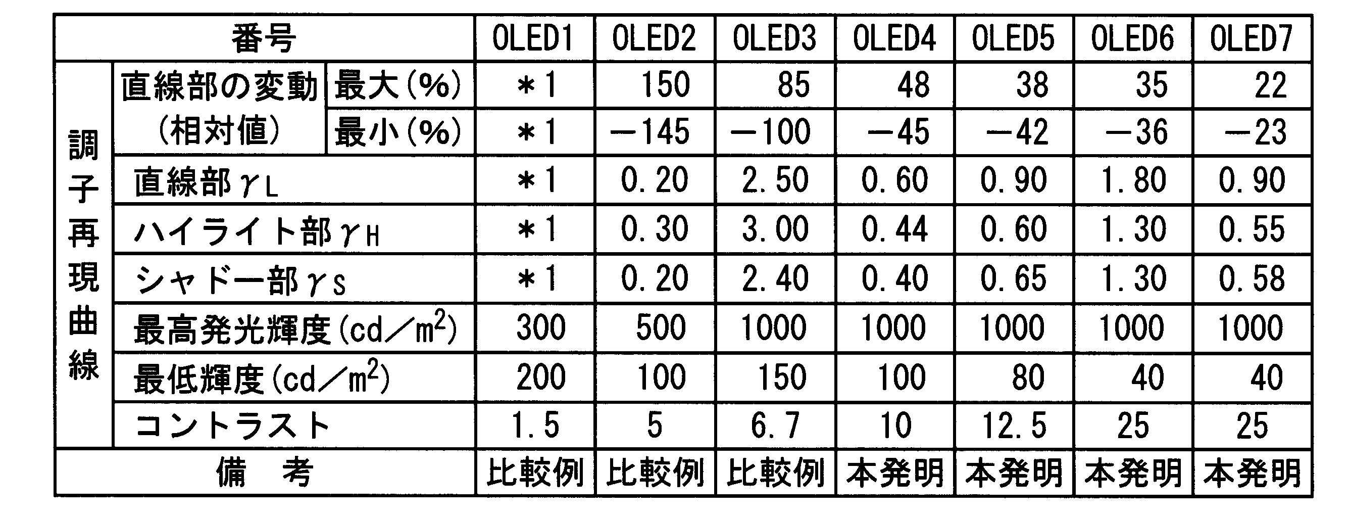

実施例1と同様の有機EL素子、手法を用いてsRGB色空間での鑑賞を前提とした、RGBそれぞれ8ビットの信号値を有する風景画像の出力を行った。
実施例1の発光パターンを有する有機EL素子4の作製と同様にして、発光パターンを有する有機EL素子8~13を作製した。
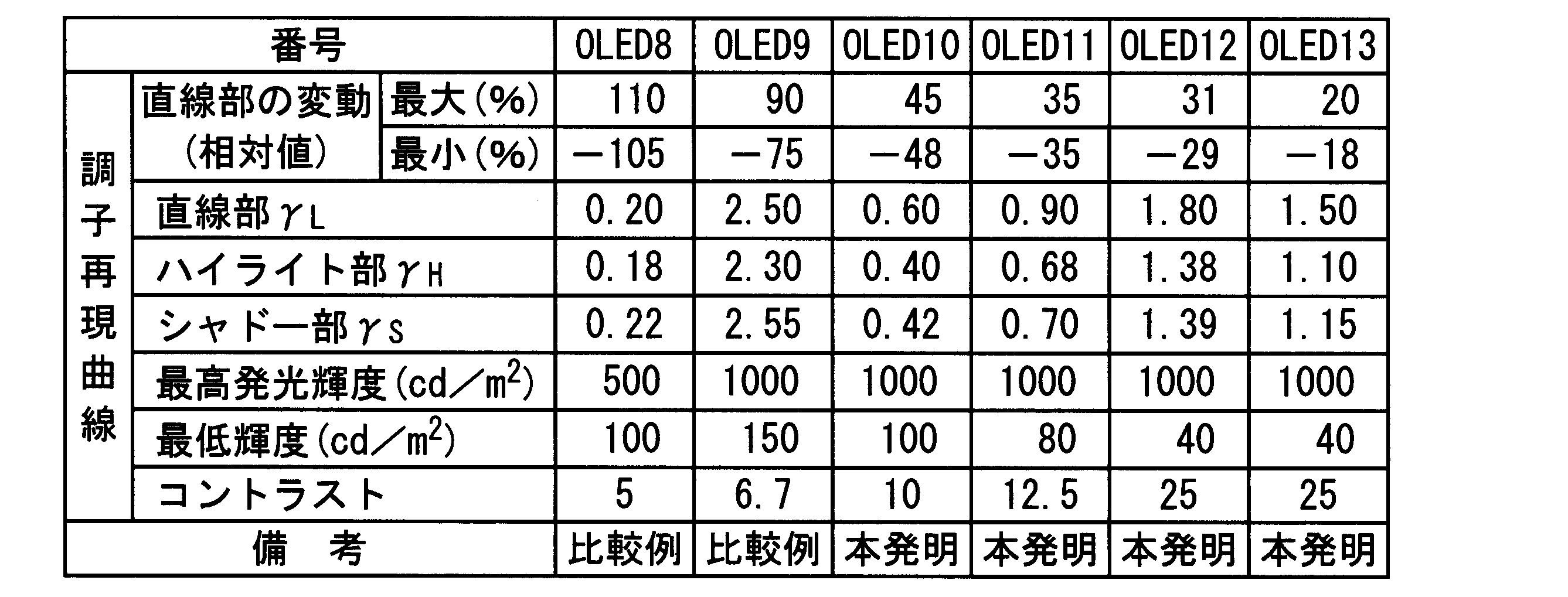

1a 下地層
1b 電極層
3 有機機能層
3a 正孔注入層
3b 正孔輸送層
3c 発光層
3d 電子輸送層
3e 電子注入層
5a 第二電極
10 有機EL素子
13 基板
13a 光取り出し面
15 補助電極
16 取り出し電極
17 封止材
19 接着剤
h 発光光
10 有機EL素子
Claims (5)
- 少なくとも一対の電極間に一つ又は複数の有機機能層を備えた有機エレクトロルミネッセンス素子に光照射して形成する発光パターンを有する有機エレクトロルミネッセンス素子の製造方法であって、
パターン化する画像について、あらかじめ作成した、ハイライト部とシャドウ部と直線部とからなり、かつハイライト部とシャドウ部とに直線部の階調の傾きより低い軟調な部分を有する調子再現曲線に基づき光照射量を変化させて、当該光照射量に対応した発光輝度による階調を有する発光パターンを形成することを特徴とする発光パターンを有する有機エレクトロルミネッセンス素子の製造方法。 - 前記調子再現曲線の前記直線部の階調の傾きが、0.6~2.0の範囲内であることを特徴とする請求項1に記載の発光パターンを有する有機エレクトロルミネッセンス素子の製造方法。
- 前記発光パターンを有する有機エレクトロルミネッセンス素子の最高発光輝度と最低輝度の比の値が、10以上であることを特徴とする請求項1又は請求項2に記載の発光パターンを有する有機エレクトロルミネッセンス素子の製造方法。
- 前記調子再現曲線における前記ハイライト部の軟調部分が、発光パターンを有する有機エレクトロルミネッセンス素子の最高発光輝度から、発光輝度の常用対数(log(発光輝度))単位で、少なくとも-0.20の範囲内であり、かつ前記シャドウ部の軟調部分が、光パターンを有する有機エレクトロルミネッセンス素子の最低輝度から、発光輝度の常用対数(log(発光輝度))単位で、少なくとも+0.20の範囲内であることを特徴とする請求項1から請求項3までのいずれか一項に記載の発光パターンを有する有機エレクトロルミネッセンス素子の製造方法。
- 前記光照射して形成する発光パターンが、紫外線を含む光を照射して形成する発光パターンであることを特徴とする請求項1から請求項4までのいずれか一項に記載の発光パターンを有する有機エレクトロルミネッセンス素子の製造方法。
Priority Applications (3)
| Application Number | Priority Date | Filing Date | Title |
|---|---|---|---|
| US14/888,310 US9564591B2 (en) | 2013-05-08 | 2014-05-02 | Method for producing organic electroluminescent element having light-emitting pattern |
| JP2015515869A JP6269662B2 (ja) | 2013-05-08 | 2014-05-02 | 発光パターンを有する有機エレクトロルミネッセンス素子の製造方法 |
| KR1020157031653A KR101789903B1 (ko) | 2013-05-08 | 2014-05-02 | 발광 패턴을 갖는 유기 일렉트로루미네센스 소자의 제조 방법 |
Applications Claiming Priority (2)
| Application Number | Priority Date | Filing Date | Title |
|---|---|---|---|
| JP2013-098523 | 2013-05-08 | ||
| JP2013098523 | 2013-05-08 |
Publications (1)
| Publication Number | Publication Date |
|---|---|
| WO2014181770A1 true WO2014181770A1 (ja) | 2014-11-13 |
Family
ID=51867250
Family Applications (1)
| Application Number | Title | Priority Date | Filing Date |
|---|---|---|---|
| PCT/JP2014/062155 Ceased WO2014181770A1 (ja) | 2013-05-08 | 2014-05-02 | 発光パターンを有する有機エレクトロルミネッセンス素子の製造方法 |
Country Status (4)
| Country | Link |
|---|---|
| US (1) | US9564591B2 (ja) |
| JP (1) | JP6269662B2 (ja) |
| KR (1) | KR101789903B1 (ja) |
| WO (1) | WO2014181770A1 (ja) |
Families Citing this family (2)
| Publication number | Priority date | Publication date | Assignee | Title |
|---|---|---|---|---|
| CN106133750B (zh) | 2014-02-04 | 2020-08-28 | 弗劳恩霍夫应用研究促进协会 | 用于确定视线方向的3d图像分析器 |
| US20230001447A1 (en) * | 2021-05-21 | 2023-01-05 | Idemitsu Kosan Co.,Ltd. | Mixed powder, method of vapor-depositing organic compound, method of fabricating organic electroluminescence device, method of selecting organic compounds, and method of vapor-depositing |
Citations (3)
| Publication number | Priority date | Publication date | Assignee | Title |
|---|---|---|---|---|
| JP2008135306A (ja) * | 2006-11-29 | 2008-06-12 | Yamagata Promotional Organization For Industrial Technology | 有機エレクトロルミネッセンス素子のパターン化方法 |
| JP2009535779A (ja) * | 2006-05-04 | 2009-10-01 | エルジー・ケム・リミテッド | 発光パターンを有する有機発光素子、その製造方法および装置 |
| JP2012134069A (ja) * | 2010-12-22 | 2012-07-12 | Fujifilm Corp | 有機電界発光素子及びその製造方法 |
Family Cites Families (4)
| Publication number | Priority date | Publication date | Assignee | Title |
|---|---|---|---|---|
| JP2793373B2 (ja) | 1991-02-07 | 1998-09-03 | 出光興産株式会社 | 有機エレクトロルミネッセンス素子のパターン化方法 |
| JPH10181103A (ja) * | 1996-11-08 | 1998-07-07 | Fuji Photo Film Co Ltd | プリンタ |
| CN1670791B (zh) * | 2004-02-12 | 2010-11-10 | 精工爱普生株式会社 | 光学显示装置及图像显示方法 |
| WO2014175135A1 (ja) * | 2013-04-26 | 2014-10-30 | コニカミノルタ株式会社 | 有機エレクトロルミネッセンス素子のパターン形成方法 |
-
2014
- 2014-05-02 US US14/888,310 patent/US9564591B2/en not_active Expired - Fee Related
- 2014-05-02 WO PCT/JP2014/062155 patent/WO2014181770A1/ja not_active Ceased
- 2014-05-02 KR KR1020157031653A patent/KR101789903B1/ko not_active Expired - Fee Related
- 2014-05-02 JP JP2015515869A patent/JP6269662B2/ja not_active Expired - Fee Related
Patent Citations (3)
| Publication number | Priority date | Publication date | Assignee | Title |
|---|---|---|---|---|
| JP2009535779A (ja) * | 2006-05-04 | 2009-10-01 | エルジー・ケム・リミテッド | 発光パターンを有する有機発光素子、その製造方法および装置 |
| JP2008135306A (ja) * | 2006-11-29 | 2008-06-12 | Yamagata Promotional Organization For Industrial Technology | 有機エレクトロルミネッセンス素子のパターン化方法 |
| JP2012134069A (ja) * | 2010-12-22 | 2012-07-12 | Fujifilm Corp | 有機電界発光素子及びその製造方法 |
Also Published As
| Publication number | Publication date |
|---|---|
| US9564591B2 (en) | 2017-02-07 |
| KR101789903B1 (ko) | 2017-10-25 |
| US20160079538A1 (en) | 2016-03-17 |
| JPWO2014181770A1 (ja) | 2017-02-23 |
| JP6269662B2 (ja) | 2018-01-31 |
| KR20150140341A (ko) | 2015-12-15 |
Similar Documents
| Publication | Publication Date | Title |
|---|---|---|
| US20210011987A1 (en) | Optical fingerprint authentication device | |
| TW594619B (en) | Organic electroluminescent display panel | |
| JP2004079422A (ja) | 有機el素子 | |
| CN103165819A (zh) | 用于有机装置的分裂电极 | |
| WO2020012685A1 (ja) | 薄膜、電子デバイス、有機エレクトロルミネッセンス素子、有機エレクトロルミネッセンス用材料、表示装置、及び、照明装置 | |
| CN106374048B (zh) | 有机发光元件 | |
| JP6269662B2 (ja) | 発光パターンを有する有機エレクトロルミネッセンス素子の製造方法 | |
| JP6319301B2 (ja) | 有機エレクトロルミネッセンス素子の製造方法 | |
| JP6340911B2 (ja) | 有機電界発光素子および有機電界発光素子の製造方法 | |
| JP6358250B2 (ja) | 有機エレクトロルミネッセンス素子のパターン形成方法 | |
| JP2017154283A (ja) | バリアフィルム、バリアフィルムの製造方法、およびそのバリアフィルムを用いた素子 | |
| JP6264374B2 (ja) | 発光パターンを備えた面発光パネルの製造方法 | |
| JP6330803B2 (ja) | 有機エレクトロルミネッセンス素子の製造方法 | |
| JP4394639B2 (ja) | 半導体薄膜の積層体、積層体の製造方法 | |
| CN112310301B (zh) | 一种有机电致发光器件及其制备方法与制备的显示装置 | |
| WO2016072246A1 (ja) | 有機エレクトロルミネッセンス素子 | |
| JP2007103093A (ja) | 有機電界発光素子 | |
| JPWO2017057023A1 (ja) | 有機エレクトロルミネッセンス素子 | |
| CN101176384A (zh) | 有机电致发光元件 | |
| WO2014181695A1 (ja) | 有機エレクトロルミネッセンス素子 | |
| JP2008218430A (ja) | 有機エレクトロルミネッセンス素子 | |
| JP2010171204A (ja) | 有機電界発光素子 | |
| JPH11312589A (ja) | 有機el素子 | |
| WO2018211776A1 (ja) | 有機エレクトロルミネッセンス素子およびその製造方法 | |
| WO2018051617A1 (ja) | 有機エレクトロルミネッセンス素子 |
Legal Events
| Date | Code | Title | Description |
|---|---|---|---|
| 121 | Ep: the epo has been informed by wipo that ep was designated in this application |
Ref document number: 14795329 Country of ref document: EP Kind code of ref document: A1 |
|
| ENP | Entry into the national phase |
Ref document number: 2015515869 Country of ref document: JP Kind code of ref document: A |
|
| WWE | Wipo information: entry into national phase |
Ref document number: 14888310 Country of ref document: US |
|
| ENP | Entry into the national phase |
Ref document number: 20157031653 Country of ref document: KR Kind code of ref document: A |
|
| NENP | Non-entry into the national phase |
Ref country code: DE |
|
| 122 | Ep: pct application non-entry in european phase |
Ref document number: 14795329 Country of ref document: EP Kind code of ref document: A1 |