WO2014175459A1 - 複合積層体および電子装置 - Google Patents
複合積層体および電子装置 Download PDFInfo
- Publication number
- WO2014175459A1 WO2014175459A1 PCT/JP2014/061916 JP2014061916W WO2014175459A1 WO 2014175459 A1 WO2014175459 A1 WO 2014175459A1 JP 2014061916 W JP2014061916 W JP 2014061916W WO 2014175459 A1 WO2014175459 A1 WO 2014175459A1
- Authority
- WO
- WIPO (PCT)
- Prior art keywords
- metal layer
- layer
- metal
- composite laminate
- group
- Prior art date
Links
Images


Classifications
-
- B—PERFORMING OPERATIONS; TRANSPORTING
- B32—LAYERED PRODUCTS
- B32B—LAYERED PRODUCTS, i.e. PRODUCTS BUILT-UP OF STRATA OF FLAT OR NON-FLAT, e.g. CELLULAR OR HONEYCOMB, FORM
- B32B15/00—Layered products comprising a layer of metal
- B32B15/01—Layered products comprising a layer of metal all layers being exclusively metallic
- B32B15/018—Layered products comprising a layer of metal all layers being exclusively metallic one layer being formed of a noble metal or a noble metal alloy
-
- B—PERFORMING OPERATIONS; TRANSPORTING
- B23—MACHINE TOOLS; METAL-WORKING NOT OTHERWISE PROVIDED FOR
- B23K—SOLDERING OR UNSOLDERING; WELDING; CLADDING OR PLATING BY SOLDERING OR WELDING; CUTTING BY APPLYING HEAT LOCALLY, e.g. FLAME CUTTING; WORKING BY LASER BEAM
- B23K35/00—Rods, electrodes, materials, or media, for use in soldering, welding, or cutting
- B23K35/22—Rods, electrodes, materials, or media, for use in soldering, welding, or cutting characterised by the composition or nature of the material
- B23K35/24—Selection of soldering or welding materials proper
- B23K35/30—Selection of soldering or welding materials proper with the principal constituent melting at less than 1550 degrees C
- B23K35/3006—Ag as the principal constituent
-
- B—PERFORMING OPERATIONS; TRANSPORTING
- B32—LAYERED PRODUCTS
- B32B—LAYERED PRODUCTS, i.e. PRODUCTS BUILT-UP OF STRATA OF FLAT OR NON-FLAT, e.g. CELLULAR OR HONEYCOMB, FORM
- B32B15/00—Layered products comprising a layer of metal
- B32B15/01—Layered products comprising a layer of metal all layers being exclusively metallic
-
- B—PERFORMING OPERATIONS; TRANSPORTING
- B32—LAYERED PRODUCTS
- B32B—LAYERED PRODUCTS, i.e. PRODUCTS BUILT-UP OF STRATA OF FLAT OR NON-FLAT, e.g. CELLULAR OR HONEYCOMB, FORM
- B32B15/00—Layered products comprising a layer of metal
- B32B15/04—Layered products comprising a layer of metal comprising metal as the main or only constituent of a layer, which is next to another layer of the same or of a different material
- B32B15/043—Layered products comprising a layer of metal comprising metal as the main or only constituent of a layer, which is next to another layer of the same or of a different material of metal
-
- B—PERFORMING OPERATIONS; TRANSPORTING
- B32—LAYERED PRODUCTS
- B32B—LAYERED PRODUCTS, i.e. PRODUCTS BUILT-UP OF STRATA OF FLAT OR NON-FLAT, e.g. CELLULAR OR HONEYCOMB, FORM
- B32B15/00—Layered products comprising a layer of metal
- B32B15/20—Layered products comprising a layer of metal comprising aluminium or copper
-
- B—PERFORMING OPERATIONS; TRANSPORTING
- B32—LAYERED PRODUCTS
- B32B—LAYERED PRODUCTS, i.e. PRODUCTS BUILT-UP OF STRATA OF FLAT OR NON-FLAT, e.g. CELLULAR OR HONEYCOMB, FORM
- B32B18/00—Layered products essentially comprising ceramics, e.g. refractory products
-
- B—PERFORMING OPERATIONS; TRANSPORTING
- B32—LAYERED PRODUCTS
- B32B—LAYERED PRODUCTS, i.e. PRODUCTS BUILT-UP OF STRATA OF FLAT OR NON-FLAT, e.g. CELLULAR OR HONEYCOMB, FORM
- B32B3/00—Layered products comprising a layer with external or internal discontinuities or unevennesses, or a layer of non-planar form; Layered products having particular features of form
- B32B3/26—Layered products comprising a layer with external or internal discontinuities or unevennesses, or a layer of non-planar form; Layered products having particular features of form characterised by a particular shape of the outline of the cross-section of a continuous layer; characterised by a layer with cavities or internal voids ; characterised by an apertured layer
-
- B—PERFORMING OPERATIONS; TRANSPORTING
- B32—LAYERED PRODUCTS
- B32B—LAYERED PRODUCTS, i.e. PRODUCTS BUILT-UP OF STRATA OF FLAT OR NON-FLAT, e.g. CELLULAR OR HONEYCOMB, FORM
- B32B7/00—Layered products characterised by the relation between layers; Layered products characterised by the relative orientation of features between layers, or by the relative values of a measurable parameter between layers, i.e. products comprising layers having different physical, chemical or physicochemical properties; Layered products characterised by the interconnection of layers
- B32B7/02—Physical, chemical or physicochemical properties
- B32B7/022—Mechanical properties
-
- B—PERFORMING OPERATIONS; TRANSPORTING
- B32—LAYERED PRODUCTS
- B32B—LAYERED PRODUCTS, i.e. PRODUCTS BUILT-UP OF STRATA OF FLAT OR NON-FLAT, e.g. CELLULAR OR HONEYCOMB, FORM
- B32B7/00—Layered products characterised by the relation between layers; Layered products characterised by the relative orientation of features between layers, or by the relative values of a measurable parameter between layers, i.e. products comprising layers having different physical, chemical or physicochemical properties; Layered products characterised by the interconnection of layers
- B32B7/02—Physical, chemical or physicochemical properties
- B32B7/027—Thermal properties
-
- B—PERFORMING OPERATIONS; TRANSPORTING
- B32—LAYERED PRODUCTS
- B32B—LAYERED PRODUCTS, i.e. PRODUCTS BUILT-UP OF STRATA OF FLAT OR NON-FLAT, e.g. CELLULAR OR HONEYCOMB, FORM
- B32B7/00—Layered products characterised by the relation between layers; Layered products characterised by the relative orientation of features between layers, or by the relative values of a measurable parameter between layers, i.e. products comprising layers having different physical, chemical or physicochemical properties; Layered products characterised by the interconnection of layers
- B32B7/04—Interconnection of layers
- B32B7/12—Interconnection of layers using interposed adhesives or interposed materials with bonding properties
-
- B—PERFORMING OPERATIONS; TRANSPORTING
- B32—LAYERED PRODUCTS
- B32B—LAYERED PRODUCTS, i.e. PRODUCTS BUILT-UP OF STRATA OF FLAT OR NON-FLAT, e.g. CELLULAR OR HONEYCOMB, FORM
- B32B9/00—Layered products comprising a layer of a particular substance not covered by groups B32B11/00 - B32B29/00
- B32B9/005—Layered products comprising a layer of a particular substance not covered by groups B32B11/00 - B32B29/00 comprising one layer of ceramic material, e.g. porcelain, ceramic tile
-
- B—PERFORMING OPERATIONS; TRANSPORTING
- B32—LAYERED PRODUCTS
- B32B—LAYERED PRODUCTS, i.e. PRODUCTS BUILT-UP OF STRATA OF FLAT OR NON-FLAT, e.g. CELLULAR OR HONEYCOMB, FORM
- B32B9/00—Layered products comprising a layer of a particular substance not covered by groups B32B11/00 - B32B29/00
- B32B9/04—Layered products comprising a layer of a particular substance not covered by groups B32B11/00 - B32B29/00 comprising such particular substance as the main or only constituent of a layer, which is next to another layer of the same or of a different material
- B32B9/041—Layered products comprising a layer of a particular substance not covered by groups B32B11/00 - B32B29/00 comprising such particular substance as the main or only constituent of a layer, which is next to another layer of the same or of a different material of metal
-
- C—CHEMISTRY; METALLURGY
- C04—CEMENTS; CONCRETE; ARTIFICIAL STONE; CERAMICS; REFRACTORIES
- C04B—LIME, MAGNESIA; SLAG; CEMENTS; COMPOSITIONS THEREOF, e.g. MORTARS, CONCRETE OR LIKE BUILDING MATERIALS; ARTIFICIAL STONE; CERAMICS; REFRACTORIES; TREATMENT OF NATURAL STONE
- C04B37/00—Joining burned ceramic articles with other burned ceramic articles or other articles by heating
- C04B37/02—Joining burned ceramic articles with other burned ceramic articles or other articles by heating with metallic articles
- C04B37/023—Joining burned ceramic articles with other burned ceramic articles or other articles by heating with metallic articles characterised by the interlayer used
- C04B37/026—Joining burned ceramic articles with other burned ceramic articles or other articles by heating with metallic articles characterised by the interlayer used consisting of metals or metal salts
-
- H—ELECTRICITY
- H01—ELECTRIC ELEMENTS
- H01L—SEMICONDUCTOR DEVICES NOT COVERED BY CLASS H10
- H01L23/00—Details of semiconductor or other solid state devices
- H01L23/12—Mountings, e.g. non-detachable insulating substrates
- H01L23/13—Mountings, e.g. non-detachable insulating substrates characterised by the shape
-
- H—ELECTRICITY
- H01—ELECTRIC ELEMENTS
- H01L—SEMICONDUCTOR DEVICES NOT COVERED BY CLASS H10
- H01L23/00—Details of semiconductor or other solid state devices
- H01L23/12—Mountings, e.g. non-detachable insulating substrates
- H01L23/14—Mountings, e.g. non-detachable insulating substrates characterised by the material or its electrical properties
-
- H—ELECTRICITY
- H01—ELECTRIC ELEMENTS
- H01L—SEMICONDUCTOR DEVICES NOT COVERED BY CLASS H10
- H01L23/00—Details of semiconductor or other solid state devices
- H01L23/34—Arrangements for cooling, heating, ventilating or temperature compensation ; Temperature sensing arrangements
- H01L23/36—Selection of materials, or shaping, to facilitate cooling or heating, e.g. heatsinks
- H01L23/373—Cooling facilitated by selection of materials for the device or materials for thermal expansion adaptation, e.g. carbon
- H01L23/3735—Laminates or multilayers, e.g. direct bond copper ceramic substrates
-
- H—ELECTRICITY
- H01—ELECTRIC ELEMENTS
- H01L—SEMICONDUCTOR DEVICES NOT COVERED BY CLASS H10
- H01L23/00—Details of semiconductor or other solid state devices
- H01L23/34—Arrangements for cooling, heating, ventilating or temperature compensation ; Temperature sensing arrangements
- H01L23/36—Selection of materials, or shaping, to facilitate cooling or heating, e.g. heatsinks
- H01L23/373—Cooling facilitated by selection of materials for the device or materials for thermal expansion adaptation, e.g. carbon
- H01L23/3736—Metallic materials
-
- H—ELECTRICITY
- H01—ELECTRIC ELEMENTS
- H01L—SEMICONDUCTOR DEVICES NOT COVERED BY CLASS H10
- H01L23/00—Details of semiconductor or other solid state devices
- H01L23/48—Arrangements for conducting electric current to or from the solid state body in operation, e.g. leads, terminal arrangements ; Selection of materials therefor
- H01L23/488—Arrangements for conducting electric current to or from the solid state body in operation, e.g. leads, terminal arrangements ; Selection of materials therefor consisting of soldered or bonded constructions
- H01L23/498—Leads, i.e. metallisations or lead-frames on insulating substrates, e.g. chip carriers
- H01L23/49822—Multilayer substrates
-
- H—ELECTRICITY
- H01—ELECTRIC ELEMENTS
- H01L—SEMICONDUCTOR DEVICES NOT COVERED BY CLASS H10
- H01L23/00—Details of semiconductor or other solid state devices
- H01L23/48—Arrangements for conducting electric current to or from the solid state body in operation, e.g. leads, terminal arrangements ; Selection of materials therefor
- H01L23/488—Arrangements for conducting electric current to or from the solid state body in operation, e.g. leads, terminal arrangements ; Selection of materials therefor consisting of soldered or bonded constructions
- H01L23/498—Leads, i.e. metallisations or lead-frames on insulating substrates, e.g. chip carriers
- H01L23/49866—Leads, i.e. metallisations or lead-frames on insulating substrates, e.g. chip carriers characterised by the materials
-
- H—ELECTRICITY
- H05—ELECTRIC TECHNIQUES NOT OTHERWISE PROVIDED FOR
- H05K—PRINTED CIRCUITS; CASINGS OR CONSTRUCTIONAL DETAILS OF ELECTRIC APPARATUS; MANUFACTURE OF ASSEMBLAGES OF ELECTRICAL COMPONENTS
- H05K1/00—Printed circuits
- H05K1/02—Details
- H05K1/09—Use of materials for the conductive, e.g. metallic pattern
-
- B—PERFORMING OPERATIONS; TRANSPORTING
- B32—LAYERED PRODUCTS
- B32B—LAYERED PRODUCTS, i.e. PRODUCTS BUILT-UP OF STRATA OF FLAT OR NON-FLAT, e.g. CELLULAR OR HONEYCOMB, FORM
- B32B2250/00—Layers arrangement
- B32B2250/04—4 layers
-
- B—PERFORMING OPERATIONS; TRANSPORTING
- B32—LAYERED PRODUCTS
- B32B—LAYERED PRODUCTS, i.e. PRODUCTS BUILT-UP OF STRATA OF FLAT OR NON-FLAT, e.g. CELLULAR OR HONEYCOMB, FORM
- B32B2250/00—Layers arrangement
- B32B2250/05—5 or more layers
-
- B—PERFORMING OPERATIONS; TRANSPORTING
- B32—LAYERED PRODUCTS
- B32B—LAYERED PRODUCTS, i.e. PRODUCTS BUILT-UP OF STRATA OF FLAT OR NON-FLAT, e.g. CELLULAR OR HONEYCOMB, FORM
- B32B2255/00—Coating on the layer surface
- B32B2255/06—Coating on the layer surface on metal layer
-
- B—PERFORMING OPERATIONS; TRANSPORTING
- B32—LAYERED PRODUCTS
- B32B—LAYERED PRODUCTS, i.e. PRODUCTS BUILT-UP OF STRATA OF FLAT OR NON-FLAT, e.g. CELLULAR OR HONEYCOMB, FORM
- B32B2255/00—Coating on the layer surface
- B32B2255/20—Inorganic coating
- B32B2255/205—Metallic coating
-
- B—PERFORMING OPERATIONS; TRANSPORTING
- B32—LAYERED PRODUCTS
- B32B—LAYERED PRODUCTS, i.e. PRODUCTS BUILT-UP OF STRATA OF FLAT OR NON-FLAT, e.g. CELLULAR OR HONEYCOMB, FORM
- B32B2307/00—Properties of the layers or laminate
- B32B2307/20—Properties of the layers or laminate having particular electrical or magnetic properties, e.g. piezoelectric
- B32B2307/202—Conductive
-
- B—PERFORMING OPERATIONS; TRANSPORTING
- B32—LAYERED PRODUCTS
- B32B—LAYERED PRODUCTS, i.e. PRODUCTS BUILT-UP OF STRATA OF FLAT OR NON-FLAT, e.g. CELLULAR OR HONEYCOMB, FORM
- B32B2307/00—Properties of the layers or laminate
- B32B2307/30—Properties of the layers or laminate having particular thermal properties
- B32B2307/302—Conductive
-
- B—PERFORMING OPERATIONS; TRANSPORTING
- B32—LAYERED PRODUCTS
- B32B—LAYERED PRODUCTS, i.e. PRODUCTS BUILT-UP OF STRATA OF FLAT OR NON-FLAT, e.g. CELLULAR OR HONEYCOMB, FORM
- B32B2307/00—Properties of the layers or laminate
- B32B2307/50—Properties of the layers or laminate having particular mechanical properties
- B32B2307/546—Flexural strength; Flexion stiffness
-
- B—PERFORMING OPERATIONS; TRANSPORTING
- B32—LAYERED PRODUCTS
- B32B—LAYERED PRODUCTS, i.e. PRODUCTS BUILT-UP OF STRATA OF FLAT OR NON-FLAT, e.g. CELLULAR OR HONEYCOMB, FORM
- B32B2307/00—Properties of the layers or laminate
- B32B2307/70—Other properties
- B32B2307/732—Dimensional properties
-
- B—PERFORMING OPERATIONS; TRANSPORTING
- B32—LAYERED PRODUCTS
- B32B—LAYERED PRODUCTS, i.e. PRODUCTS BUILT-UP OF STRATA OF FLAT OR NON-FLAT, e.g. CELLULAR OR HONEYCOMB, FORM
- B32B2307/00—Properties of the layers or laminate
- B32B2307/70—Other properties
- B32B2307/748—Releasability
-
- B—PERFORMING OPERATIONS; TRANSPORTING
- B32—LAYERED PRODUCTS
- B32B—LAYERED PRODUCTS, i.e. PRODUCTS BUILT-UP OF STRATA OF FLAT OR NON-FLAT, e.g. CELLULAR OR HONEYCOMB, FORM
- B32B2457/00—Electrical equipment
- B32B2457/14—Semiconductor wafers
-
- C—CHEMISTRY; METALLURGY
- C04—CEMENTS; CONCRETE; ARTIFICIAL STONE; CERAMICS; REFRACTORIES
- C04B—LIME, MAGNESIA; SLAG; CEMENTS; COMPOSITIONS THEREOF, e.g. MORTARS, CONCRETE OR LIKE BUILDING MATERIALS; ARTIFICIAL STONE; CERAMICS; REFRACTORIES; TREATMENT OF NATURAL STONE
- C04B2237/00—Aspects relating to ceramic laminates or to joining of ceramic articles with other articles by heating
- C04B2237/02—Aspects relating to interlayers, e.g. used to join ceramic articles with other articles by heating
- C04B2237/12—Metallic interlayers
- C04B2237/122—Metallic interlayers based on refractory metals
-
- C—CHEMISTRY; METALLURGY
- C04—CEMENTS; CONCRETE; ARTIFICIAL STONE; CERAMICS; REFRACTORIES
- C04B—LIME, MAGNESIA; SLAG; CEMENTS; COMPOSITIONS THEREOF, e.g. MORTARS, CONCRETE OR LIKE BUILDING MATERIALS; ARTIFICIAL STONE; CERAMICS; REFRACTORIES; TREATMENT OF NATURAL STONE
- C04B2237/00—Aspects relating to ceramic laminates or to joining of ceramic articles with other articles by heating
- C04B2237/02—Aspects relating to interlayers, e.g. used to join ceramic articles with other articles by heating
- C04B2237/12—Metallic interlayers
- C04B2237/123—Metallic interlayers based on iron group metals, e.g. steel
-
- C—CHEMISTRY; METALLURGY
- C04—CEMENTS; CONCRETE; ARTIFICIAL STONE; CERAMICS; REFRACTORIES
- C04B—LIME, MAGNESIA; SLAG; CEMENTS; COMPOSITIONS THEREOF, e.g. MORTARS, CONCRETE OR LIKE BUILDING MATERIALS; ARTIFICIAL STONE; CERAMICS; REFRACTORIES; TREATMENT OF NATURAL STONE
- C04B2237/00—Aspects relating to ceramic laminates or to joining of ceramic articles with other articles by heating
- C04B2237/02—Aspects relating to interlayers, e.g. used to join ceramic articles with other articles by heating
- C04B2237/12—Metallic interlayers
- C04B2237/124—Metallic interlayers based on copper
-
- C—CHEMISTRY; METALLURGY
- C04—CEMENTS; CONCRETE; ARTIFICIAL STONE; CERAMICS; REFRACTORIES
- C04B—LIME, MAGNESIA; SLAG; CEMENTS; COMPOSITIONS THEREOF, e.g. MORTARS, CONCRETE OR LIKE BUILDING MATERIALS; ARTIFICIAL STONE; CERAMICS; REFRACTORIES; TREATMENT OF NATURAL STONE
- C04B2237/00—Aspects relating to ceramic laminates or to joining of ceramic articles with other articles by heating
- C04B2237/02—Aspects relating to interlayers, e.g. used to join ceramic articles with other articles by heating
- C04B2237/12—Metallic interlayers
- C04B2237/125—Metallic interlayers based on noble metals, e.g. silver
-
- C—CHEMISTRY; METALLURGY
- C04—CEMENTS; CONCRETE; ARTIFICIAL STONE; CERAMICS; REFRACTORIES
- C04B—LIME, MAGNESIA; SLAG; CEMENTS; COMPOSITIONS THEREOF, e.g. MORTARS, CONCRETE OR LIKE BUILDING MATERIALS; ARTIFICIAL STONE; CERAMICS; REFRACTORIES; TREATMENT OF NATURAL STONE
- C04B2237/00—Aspects relating to ceramic laminates or to joining of ceramic articles with other articles by heating
- C04B2237/02—Aspects relating to interlayers, e.g. used to join ceramic articles with other articles by heating
- C04B2237/12—Metallic interlayers
- C04B2237/126—Metallic interlayers wherein the active component for bonding is not the largest fraction of the interlayer
- C04B2237/127—The active component for bonding being a refractory metal
-
- C—CHEMISTRY; METALLURGY
- C04—CEMENTS; CONCRETE; ARTIFICIAL STONE; CERAMICS; REFRACTORIES
- C04B—LIME, MAGNESIA; SLAG; CEMENTS; COMPOSITIONS THEREOF, e.g. MORTARS, CONCRETE OR LIKE BUILDING MATERIALS; ARTIFICIAL STONE; CERAMICS; REFRACTORIES; TREATMENT OF NATURAL STONE
- C04B2237/00—Aspects relating to ceramic laminates or to joining of ceramic articles with other articles by heating
- C04B2237/30—Composition of layers of ceramic laminates or of ceramic or metallic articles to be joined by heating, e.g. Si substrates
- C04B2237/32—Ceramic
- C04B2237/34—Oxidic
- C04B2237/341—Silica or silicates
-
- C—CHEMISTRY; METALLURGY
- C04—CEMENTS; CONCRETE; ARTIFICIAL STONE; CERAMICS; REFRACTORIES
- C04B—LIME, MAGNESIA; SLAG; CEMENTS; COMPOSITIONS THEREOF, e.g. MORTARS, CONCRETE OR LIKE BUILDING MATERIALS; ARTIFICIAL STONE; CERAMICS; REFRACTORIES; TREATMENT OF NATURAL STONE
- C04B2237/00—Aspects relating to ceramic laminates or to joining of ceramic articles with other articles by heating
- C04B2237/30—Composition of layers of ceramic laminates or of ceramic or metallic articles to be joined by heating, e.g. Si substrates
- C04B2237/32—Ceramic
- C04B2237/34—Oxidic
- C04B2237/343—Alumina or aluminates
-
- C—CHEMISTRY; METALLURGY
- C04—CEMENTS; CONCRETE; ARTIFICIAL STONE; CERAMICS; REFRACTORIES
- C04B—LIME, MAGNESIA; SLAG; CEMENTS; COMPOSITIONS THEREOF, e.g. MORTARS, CONCRETE OR LIKE BUILDING MATERIALS; ARTIFICIAL STONE; CERAMICS; REFRACTORIES; TREATMENT OF NATURAL STONE
- C04B2237/00—Aspects relating to ceramic laminates or to joining of ceramic articles with other articles by heating
- C04B2237/30—Composition of layers of ceramic laminates or of ceramic or metallic articles to be joined by heating, e.g. Si substrates
- C04B2237/32—Ceramic
- C04B2237/36—Non-oxidic
- C04B2237/365—Silicon carbide
-
- C—CHEMISTRY; METALLURGY
- C04—CEMENTS; CONCRETE; ARTIFICIAL STONE; CERAMICS; REFRACTORIES
- C04B—LIME, MAGNESIA; SLAG; CEMENTS; COMPOSITIONS THEREOF, e.g. MORTARS, CONCRETE OR LIKE BUILDING MATERIALS; ARTIFICIAL STONE; CERAMICS; REFRACTORIES; TREATMENT OF NATURAL STONE
- C04B2237/00—Aspects relating to ceramic laminates or to joining of ceramic articles with other articles by heating
- C04B2237/30—Composition of layers of ceramic laminates or of ceramic or metallic articles to be joined by heating, e.g. Si substrates
- C04B2237/32—Ceramic
- C04B2237/36—Non-oxidic
- C04B2237/366—Aluminium nitride
-
- C—CHEMISTRY; METALLURGY
- C04—CEMENTS; CONCRETE; ARTIFICIAL STONE; CERAMICS; REFRACTORIES
- C04B—LIME, MAGNESIA; SLAG; CEMENTS; COMPOSITIONS THEREOF, e.g. MORTARS, CONCRETE OR LIKE BUILDING MATERIALS; ARTIFICIAL STONE; CERAMICS; REFRACTORIES; TREATMENT OF NATURAL STONE
- C04B2237/00—Aspects relating to ceramic laminates or to joining of ceramic articles with other articles by heating
- C04B2237/30—Composition of layers of ceramic laminates or of ceramic or metallic articles to be joined by heating, e.g. Si substrates
- C04B2237/32—Ceramic
- C04B2237/36—Non-oxidic
- C04B2237/368—Silicon nitride
-
- C—CHEMISTRY; METALLURGY
- C04—CEMENTS; CONCRETE; ARTIFICIAL STONE; CERAMICS; REFRACTORIES
- C04B—LIME, MAGNESIA; SLAG; CEMENTS; COMPOSITIONS THEREOF, e.g. MORTARS, CONCRETE OR LIKE BUILDING MATERIALS; ARTIFICIAL STONE; CERAMICS; REFRACTORIES; TREATMENT OF NATURAL STONE
- C04B2237/00—Aspects relating to ceramic laminates or to joining of ceramic articles with other articles by heating
- C04B2237/30—Composition of layers of ceramic laminates or of ceramic or metallic articles to be joined by heating, e.g. Si substrates
- C04B2237/40—Metallic
- C04B2237/407—Copper
-
- C—CHEMISTRY; METALLURGY
- C04—CEMENTS; CONCRETE; ARTIFICIAL STONE; CERAMICS; REFRACTORIES
- C04B—LIME, MAGNESIA; SLAG; CEMENTS; COMPOSITIONS THEREOF, e.g. MORTARS, CONCRETE OR LIKE BUILDING MATERIALS; ARTIFICIAL STONE; CERAMICS; REFRACTORIES; TREATMENT OF NATURAL STONE
- C04B2237/00—Aspects relating to ceramic laminates or to joining of ceramic articles with other articles by heating
- C04B2237/50—Processing aspects relating to ceramic laminates or to the joining of ceramic articles with other articles by heating
- C04B2237/60—Forming at the joining interface or in the joining layer specific reaction phases or zones, e.g. diffusion of reactive species from the interlayer to the substrate or from a substrate to the joining interface, carbide forming at the joining interface
-
- C—CHEMISTRY; METALLURGY
- C04—CEMENTS; CONCRETE; ARTIFICIAL STONE; CERAMICS; REFRACTORIES
- C04B—LIME, MAGNESIA; SLAG; CEMENTS; COMPOSITIONS THEREOF, e.g. MORTARS, CONCRETE OR LIKE BUILDING MATERIALS; ARTIFICIAL STONE; CERAMICS; REFRACTORIES; TREATMENT OF NATURAL STONE
- C04B2237/00—Aspects relating to ceramic laminates or to joining of ceramic articles with other articles by heating
- C04B2237/50—Processing aspects relating to ceramic laminates or to the joining of ceramic articles with other articles by heating
- C04B2237/70—Forming laminates or joined articles comprising layers of a specific, unusual thickness
- C04B2237/706—Forming laminates or joined articles comprising layers of a specific, unusual thickness of one or more of the metallic layers or articles
-
- C—CHEMISTRY; METALLURGY
- C04—CEMENTS; CONCRETE; ARTIFICIAL STONE; CERAMICS; REFRACTORIES
- C04B—LIME, MAGNESIA; SLAG; CEMENTS; COMPOSITIONS THEREOF, e.g. MORTARS, CONCRETE OR LIKE BUILDING MATERIALS; ARTIFICIAL STONE; CERAMICS; REFRACTORIES; TREATMENT OF NATURAL STONE
- C04B2237/00—Aspects relating to ceramic laminates or to joining of ceramic articles with other articles by heating
- C04B2237/50—Processing aspects relating to ceramic laminates or to the joining of ceramic articles with other articles by heating
- C04B2237/70—Forming laminates or joined articles comprising layers of a specific, unusual thickness
- C04B2237/708—Forming laminates or joined articles comprising layers of a specific, unusual thickness of one or more of the interlayers
-
- C—CHEMISTRY; METALLURGY
- C04—CEMENTS; CONCRETE; ARTIFICIAL STONE; CERAMICS; REFRACTORIES
- C04B—LIME, MAGNESIA; SLAG; CEMENTS; COMPOSITIONS THEREOF, e.g. MORTARS, CONCRETE OR LIKE BUILDING MATERIALS; ARTIFICIAL STONE; CERAMICS; REFRACTORIES; TREATMENT OF NATURAL STONE
- C04B2237/00—Aspects relating to ceramic laminates or to joining of ceramic articles with other articles by heating
- C04B2237/50—Processing aspects relating to ceramic laminates or to the joining of ceramic articles with other articles by heating
- C04B2237/72—Forming laminates or joined articles comprising at least two interlayers directly next to each other
-
- H—ELECTRICITY
- H01—ELECTRIC ELEMENTS
- H01L—SEMICONDUCTOR DEVICES NOT COVERED BY CLASS H10
- H01L2224/00—Indexing scheme for arrangements for connecting or disconnecting semiconductor or solid-state bodies and methods related thereto as covered by H01L24/00
- H01L2224/01—Means for bonding being attached to, or being formed on, the surface to be connected, e.g. chip-to-package, die-attach, "first-level" interconnects; Manufacturing methods related thereto
- H01L2224/26—Layer connectors, e.g. plate connectors, solder or adhesive layers; Manufacturing methods related thereto
- H01L2224/31—Structure, shape, material or disposition of the layer connectors after the connecting process
- H01L2224/32—Structure, shape, material or disposition of the layer connectors after the connecting process of an individual layer connector
- H01L2224/321—Disposition
- H01L2224/32151—Disposition the layer connector connecting between a semiconductor or solid-state body and an item not being a semiconductor or solid-state body, e.g. chip-to-substrate, chip-to-passive
- H01L2224/32221—Disposition the layer connector connecting between a semiconductor or solid-state body and an item not being a semiconductor or solid-state body, e.g. chip-to-substrate, chip-to-passive the body and the item being stacked
- H01L2224/32225—Disposition the layer connector connecting between a semiconductor or solid-state body and an item not being a semiconductor or solid-state body, e.g. chip-to-substrate, chip-to-passive the body and the item being stacked the item being non-metallic, e.g. insulating substrate with or without metallisation
-
- H—ELECTRICITY
- H01—ELECTRIC ELEMENTS
- H01L—SEMICONDUCTOR DEVICES NOT COVERED BY CLASS H10
- H01L2224/00—Indexing scheme for arrangements for connecting or disconnecting semiconductor or solid-state bodies and methods related thereto as covered by H01L24/00
- H01L2224/01—Means for bonding being attached to, or being formed on, the surface to be connected, e.g. chip-to-package, die-attach, "first-level" interconnects; Manufacturing methods related thereto
- H01L2224/42—Wire connectors; Manufacturing methods related thereto
- H01L2224/47—Structure, shape, material or disposition of the wire connectors after the connecting process
- H01L2224/48—Structure, shape, material or disposition of the wire connectors after the connecting process of an individual wire connector
- H01L2224/4805—Shape
- H01L2224/4809—Loop shape
- H01L2224/48091—Arched
-
- H—ELECTRICITY
- H01—ELECTRIC ELEMENTS
- H01L—SEMICONDUCTOR DEVICES NOT COVERED BY CLASS H10
- H01L2224/00—Indexing scheme for arrangements for connecting or disconnecting semiconductor or solid-state bodies and methods related thereto as covered by H01L24/00
- H01L2224/01—Means for bonding being attached to, or being formed on, the surface to be connected, e.g. chip-to-package, die-attach, "first-level" interconnects; Manufacturing methods related thereto
- H01L2224/42—Wire connectors; Manufacturing methods related thereto
- H01L2224/47—Structure, shape, material or disposition of the wire connectors after the connecting process
- H01L2224/48—Structure, shape, material or disposition of the wire connectors after the connecting process of an individual wire connector
- H01L2224/481—Disposition
- H01L2224/48151—Connecting between a semiconductor or solid-state body and an item not being a semiconductor or solid-state body, e.g. chip-to-substrate, chip-to-passive
- H01L2224/48221—Connecting between a semiconductor or solid-state body and an item not being a semiconductor or solid-state body, e.g. chip-to-substrate, chip-to-passive the body and the item being stacked
- H01L2224/48225—Connecting between a semiconductor or solid-state body and an item not being a semiconductor or solid-state body, e.g. chip-to-substrate, chip-to-passive the body and the item being stacked the item being non-metallic, e.g. insulating substrate with or without metallisation
- H01L2224/48227—Connecting between a semiconductor or solid-state body and an item not being a semiconductor or solid-state body, e.g. chip-to-substrate, chip-to-passive the body and the item being stacked the item being non-metallic, e.g. insulating substrate with or without metallisation connecting the wire to a bond pad of the item
-
- H—ELECTRICITY
- H01—ELECTRIC ELEMENTS
- H01L—SEMICONDUCTOR DEVICES NOT COVERED BY CLASS H10
- H01L2224/00—Indexing scheme for arrangements for connecting or disconnecting semiconductor or solid-state bodies and methods related thereto as covered by H01L24/00
- H01L2224/73—Means for bonding being of different types provided for in two or more of groups H01L2224/10, H01L2224/18, H01L2224/26, H01L2224/34, H01L2224/42, H01L2224/50, H01L2224/63, H01L2224/71
- H01L2224/732—Location after the connecting process
- H01L2224/73251—Location after the connecting process on different surfaces
- H01L2224/73265—Layer and wire connectors
-
- H—ELECTRICITY
- H01—ELECTRIC ELEMENTS
- H01L—SEMICONDUCTOR DEVICES NOT COVERED BY CLASS H10
- H01L23/00—Details of semiconductor or other solid state devices
- H01L23/12—Mountings, e.g. non-detachable insulating substrates
- H01L23/14—Mountings, e.g. non-detachable insulating substrates characterised by the material or its electrical properties
- H01L23/15—Ceramic or glass substrates
-
- H—ELECTRICITY
- H01—ELECTRIC ELEMENTS
- H01L—SEMICONDUCTOR DEVICES NOT COVERED BY CLASS H10
- H01L2924/00—Indexing scheme for arrangements or methods for connecting or disconnecting semiconductor or solid-state bodies as covered by H01L24/00
- H01L2924/10—Details of semiconductor or other solid state devices to be connected
- H01L2924/11—Device type
- H01L2924/13—Discrete devices, e.g. 3 terminal devices
- H01L2924/1304—Transistor
- H01L2924/1305—Bipolar Junction Transistor [BJT]
- H01L2924/13055—Insulated gate bipolar transistor [IGBT]
-
- H—ELECTRICITY
- H01—ELECTRIC ELEMENTS
- H01L—SEMICONDUCTOR DEVICES NOT COVERED BY CLASS H10
- H01L2924/00—Indexing scheme for arrangements or methods for connecting or disconnecting semiconductor or solid-state bodies as covered by H01L24/00
- H01L2924/10—Details of semiconductor or other solid state devices to be connected
- H01L2924/11—Device type
- H01L2924/13—Discrete devices, e.g. 3 terminal devices
- H01L2924/1304—Transistor
- H01L2924/1306—Field-effect transistor [FET]
- H01L2924/13091—Metal-Oxide-Semiconductor Field-Effect Transistor [MOSFET]
-
- H—ELECTRICITY
- H05—ELECTRIC TECHNIQUES NOT OTHERWISE PROVIDED FOR
- H05K—PRINTED CIRCUITS; CASINGS OR CONSTRUCTIONAL DETAILS OF ELECTRIC APPARATUS; MANUFACTURE OF ASSEMBLAGES OF ELECTRICAL COMPONENTS
- H05K1/00—Printed circuits
- H05K1/02—Details
- H05K1/03—Use of materials for the substrate
- H05K1/0306—Inorganic insulating substrates, e.g. ceramic, glass
-
- H—ELECTRICITY
- H05—ELECTRIC TECHNIQUES NOT OTHERWISE PROVIDED FOR
- H05K—PRINTED CIRCUITS; CASINGS OR CONSTRUCTIONAL DETAILS OF ELECTRIC APPARATUS; MANUFACTURE OF ASSEMBLAGES OF ELECTRICAL COMPONENTS
- H05K2201/00—Indexing scheme relating to printed circuits covered by H05K1/00
- H05K2201/03—Conductive materials
- H05K2201/0332—Structure of the conductor
- H05K2201/0335—Layered conductors or foils
- H05K2201/0338—Layered conductor, e.g. layered metal substrate, layered finish layer, layered thin film adhesion layer
-
- H—ELECTRICITY
- H05—ELECTRIC TECHNIQUES NOT OTHERWISE PROVIDED FOR
- H05K—PRINTED CIRCUITS; CASINGS OR CONSTRUCTIONAL DETAILS OF ELECTRIC APPARATUS; MANUFACTURE OF ASSEMBLAGES OF ELECTRICAL COMPONENTS
- H05K2203/00—Indexing scheme relating to apparatus or processes for manufacturing printed circuits covered by H05K3/00
- H05K2203/04—Soldering or other types of metallurgic bonding
- H05K2203/049—Wire bonding
-
- H—ELECTRICITY
- H05—ELECTRIC TECHNIQUES NOT OTHERWISE PROVIDED FOR
- H05K—PRINTED CIRCUITS; CASINGS OR CONSTRUCTIONAL DETAILS OF ELECTRIC APPARATUS; MANUFACTURE OF ASSEMBLAGES OF ELECTRICAL COMPONENTS
- H05K3/00—Apparatus or processes for manufacturing printed circuits
- H05K3/38—Improvement of the adhesion between the insulating substrate and the metal
- H05K3/388—Improvement of the adhesion between the insulating substrate and the metal by the use of a metallic or inorganic thin film adhesion layer
Definitions
- the present invention relates to a composite laminate and an electronic device.
- An electronic device in which an electronic element is mounted on a composite laminate is used as an IGBT (Insulated Gate Bipolar Transistor) such as a power module or a switching module.
- IGBT Insulated Gate Bipolar Transistor
- the composite laminate for example, a joined body in which a metal layer made of copper is joined to a ceramic substrate through a brazing material is used.
- the electronic element is mounted on the metal layer and is electrically connected to the metal layer by, for example, a bonding wire.
- the brazing material is peeled off from the metal layer or cracks are generated in the brazing material due to the thermal stress caused by the difference in thermal expansion coefficient between the metal layer and the ceramic substrate. There was a problem that it might be.
- the composite laminate of one embodiment of the present invention has a first metal layer, a second metal layer, a third metal layer, and a fourth layer.
- the first metal layer contains copper (Cu).
- the second metal layer is disposed on the lower surface of the first metal layer.
- the third metal layer is disposed on the lower surface of the second metal layer, and is selected from at least one metal selected from the first group consisting of Sn, Al, and Ga and from the second group consisting of In and Sb. At least one metal to be produced and silver (Ag).
- the fourth layer is disposed on the lower surface of the third metal layer.
- the third metal layer has a metal portion that partially enters from the third metal layer to the second metal layer.
- the composite laminate of another aspect of the present invention has a first metal layer, a second metal layer, and a third layer.
- the first metal layer contains copper (Cu).
- the second metal layer is disposed on the lower surface of the first metal layer.
- the third layer is disposed on the lower surface of the second metal layer.
- the second metal layer is provided with a metal portion that partially enters from the third layer to the second metal layer.
- An electronic device includes a composite laminate having the above-described configuration and an electronic component mounted on the composite laminate.
- the third metal layer has a metal portion that partially enters from the third metal layer to the second metal layer.
- a large anchor effect can be obtained between the first metal layer and the third metal layer. Therefore, since the third metal layer is firmly bonded to the first metal layer, it is possible to suppress peeling between layers inside.
- the second metal layer is provided with the metal portion partially entering from the third layer to the second metal layer.
- the three layers can obtain an anchor effect via the metal part. Therefore, since the third layer is firmly bonded to the first metal layer, it is possible to suppress peeling between layers inside.
- the composite laminated body having the above configuration since the composite laminated body having the above configuration is included, peeling between layers can be suppressed.
- the composite laminate and the electronic device are provided in a virtual xyz space and placed on the xy plane.
- the upward direction is the positive direction of the virtual z axis.
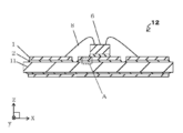
- the composite laminate 12 in this embodiment includes a first metal layer 1, a second metal layer 2, a third metal layer 3, and a fourth layer 4.
- the electronic component 6 is mounted on the first metal layer 1 to form an electronic device.
- the first metal layer 1 contains copper.
- the first metal layer 1 is used as a circuit conductor, for example.
- the first metal layer 1 can be used not only as a circuit conductor but also as a metal member for mounting an electronic component mounted on the composite laminate 12, a metal member for a ground conductor, a heat sink, or the like.
- the first metal layer 1 is used as a conductive path for supplying a relatively large current of, for example, several tens of A, or a heat dissipation material.
- the brazing material that joins both members peels off from the first metal layer 1 due to the thermal stress caused by the difference in thermal expansion coefficient between the fourth layer 4 and the first metal layer 1, or cracks occur in the brazing material.
- the composite laminate 12 has the following configuration.
- the composite laminate 12 of this embodiment is formed by sequentially laminating the first metal layer 1, the second metal layer 2, the third metal layer 3 and the fourth layer 4 in the vertical direction (z-axis direction). Yes.
- a second metal layer 2 is provided on the lower surface of the first metal layer 1
- a third metal layer 3 is provided on the lower surface of the second metal layer 2
- a fourth layer 4 is provided on the lower surface of the third metal layer 3. Is provided.
- the first metal layer 1 is made of, for example, copper or an alloy material containing copper as a main component. From the viewpoint of heat dissipation, the first metal layer 1 is made of a metal material having high thermal conductivity, and copper (Cu), which is a metal material having high thermal conductivity, is preferably used (Cu thermal conductivity: 395 W / m ⁇ K).
- a metal processing method such as a mechanical processing such as a rolling method or a punching method or a chemical processing such as etching to a Cu ingot (lump), for example, a predetermined plate shape having a thickness of 10 to 300 ⁇ m Formed into a pattern.
- the copper used for the first metal layer 1 is, for example, oxygen-free copper.
- oxygen-free copper is used as the material of the first metal layer 1, it is reduced that the copper surface is oxidized by oxygen present in the copper when the first metal layer 1 and the fourth layer 4 are joined.
- the wettability with the bonding material 7 (described later) is improved, the bonding strength between the first metal layer 1 and the fourth layer 4 is improved.
- the third metal layer 3 contains at least one metal selected from the first group consisting of Sn, Al, and Ga, at least one metal selected from the second group consisting of In, Sb, and silver. To do.
- the third metal layer 3 further contains at least one of Ti, Hf, and Zr.
- the first metal layer 1 is bonded to the fourth layer by these active metals.
- the thickness of the third metal layer 3 may be about 5 to 100 ⁇ m, for example.
- the second metal layer 2 contains an alloy containing at least one metal selected from the first group consisting of Sn, Al, and Ga, and copper.
- the second metal layer 2 is interpreted as a layer in which at least one metal selected from the first group diffused from the third metal layer 3 and copper contained in the first metal layer 1 are combined and alloyed. Good.
- the fourth layer 4 is a ceramic substrate in the embodiment shown in FIG.
- the fourth layer 4 is made of ceramics such as aluminum oxide ceramics, mullite ceramics, silicon carbide ceramics, aluminum nitride ceramics, or silicon nitride ceramics.
- ceramics such as aluminum oxide ceramics, mullite ceramics, silicon carbide ceramics, aluminum nitride ceramics, or silicon nitride ceramics.
- silicon carbide ceramics, aluminum nitride ceramics, or silicon nitride ceramics are preferred in terms of thermal conductivity that affects heat dissipation, and silicon nitride ceramics or silicon carbide ceramics in terms of strength. Is preferred.
- the fourth layer 4 is made of a relatively strong ceramic material such as silicon nitride ceramics, the possibility of cracks in the fourth layer 4 is reduced even if the first metal layer 1 having a larger thickness is used. Therefore, it is possible to realize the composite laminate 12 capable of flowing a larger current while reducing the size.
- the thickness of the fourth layer 4 may be smaller in terms of thermal conductivity, for example, about 0.1 mm to 1 mm, and may be selected according to the size of the composite laminate 12 or the thermal conductivity or strength of the material used. Good.
- the fourth layer 4 is made of, for example, silicon nitride ceramics
- an appropriate organic binder, plasticizer, and solvent are added to and mixed with raw material powders such as silicon nitride, aluminum oxide, magnesium oxide, and yttrium oxide.
- a ceramic green sheet (ceramic green sheet) is formed on the mud by using a conventionally known doctor blade method or calender roll method, and then the ceramic green sheet is subjected to a suitable punching process to obtain a predetermined shape. If necessary, a plurality of sheets are laminated to form a molded body, and thereafter, this is manufactured by firing at a temperature of 1600 to 2000 ° C. in a non-oxidizing atmosphere such as a nitriding atmosphere.
- a metal having high conductivity, good corrosion resistance, and good wettability with the brazing material may be deposited on the first metal layer 1 by a plating method.
- the first metal layer 1 and the external electric circuit, the bonding material 7 and the like can be more easily and firmly bonded. Further, the electrical connection between the first metal layer 1 and the external electric circuit or the like can be made better.
- the plating metal examples include metal materials such as nickel, cobalt, copper, and gold, or alloy materials mainly composed of these metal materials.
- metal materials such as nickel, cobalt, copper, and gold
- alloy materials mainly composed of these metal materials for example, in the case of a nickel-phosphorus amorphous alloy plating layer containing 8 to 15% by mass of phosphorus inside, the surface oxidation of the nickel plating layer can be suppressed and the wettability of the bonding material 7 and the like can be maintained for a long time. It is preferable because it is possible.
- the phosphorus content relative to nickel is about 8 to 15 masses, a nickel-phosphorus amorphous alloy is easily formed, and the adhesive strength of the bonding material 7 and the like to the plating layer can be improved.
- the thickness of the nickel plating layer may be about 1.5 to 10 ⁇ m, for example.
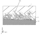
- FIG. 2 is an enlarged view of part A in FIG.
- the third metal layer 3 has a metal portion 2 ⁇ / b> A that partially enters from the third metal layer 3 to the second metal layer 2.
- a large anchor effect can be obtained between the second metal layer 2 and the third metal layer 3. Therefore, since the third metal layer 3 is firmly bonded to the first metal layer 1, it is possible to suppress peeling between layers inside.
- the width of the metal part 2A is about 20 to 100 ⁇ m.
- the length of the metal part 2A is about 50 to 150 ⁇ m.
- a plurality of metal portions 2A are provided.
- the third metal layer 3 is a bonding layer that bonds the first metal layer 1 and the fourth layer 4 together. Therefore, the third metal layer 3 has at least one metal selected from the first group consisting of Sn, Al, and Ga, which has a function as a brazing material, and at least selected from the second group consisting of In, Sb. Contains one metal and silver. For example, the third metal layer 3 is a silver-tin brazing material.
- the first metal layer 1 and the third metal layer 3 are connected to each other.
- the second metal layer 2 is provided as an alloy layer.
- the metal portion 2A made of an alloy of at least one metal selected from the second group consisting of In and Sb and Ag partially enters the second metal layer 2.
- the metal part 2A contains an Ag—In alloy.
- the alloy of the second group metal and Ag occupy 70% to 100% of the whole when the cross section is viewed. Also, in the metal part 2A, when the alloy of the second group metal and Ag occupies 70% to 100% of the whole, the remaining area of about 0 to 30% is a single Ag, Ag-In-Sn alloy , Ag-Sn alloy, In-Sn alloy and the like.
- each element is mapped by a wavelength dispersive X-ray spectrometer (WDS) on the cross section of the metal part 2A.
- WDS wavelength dispersive X-ray spectrometer
- the cross-sectional area of the alloy is calculated by calculating the area of the region where the second group of metals and Ag overlap.
- the area of a region not overlapping with other elements may be calculated.
- Such a metal portion 2A partially enters the second metal layer 2 in an intricate form as shown in FIG. 2, for example, so that the third metal layer 3 and the first metal layer 1 are interposed. A large anchor effect is obtained. Due to this anchor effect, the first metal layer 1 and the third metal layer 3 are firmly bonded to each other.
- the third metal layer 3 in the example of FIG. 2 has a form in which crystal grains of a silver-based alloy such as silver-copper are dispersed in a silver matrix. That is, the entire third metal layer 3 does not have a substantially uniform composition, but a metal component such as copper, which is a diffusion component from the first metal layer 1, is unevenly distributed in part.
- the third metal layer 3 may include a portion in which some components are unevenly distributed.
- the joining of the first metal layer 1 to the fourth layer 4 is performed by brazing.
- the first metal layer 1 is positioned and temporarily fixed to the upper surface of the fourth layer 4 via the brazing material layer, and then these are integrally heated in, for example, an electric furnace and then cooled.
- the first metal layer 1 is bonded to the fourth layer 4.
- the brazing material used in this case is the third metal layer 3.
- Specific examples of the brazing material to be the third metal layer 3 include the following. That is, in the brazing material, Ag is 30 to 70% by mass, Ti is 1 to 5% by mass, at least one metal selected from the first group is 20 to 40% by mass, and at least 1 selected from the second group One metal is about 1 to 40% by mass. More specific examples include those in which Ag is 69% by mass, Ti is 1% by mass, Sn is 20% by mass, and In is 10% by mass.
- the third metal layer 3 may contain about 1 to 20% by mass of copper in addition to the above metal components.
- a brazing material mainly composed of silver is used as at least one selected from the first group. 20-40% by weight of metal and at least one metal selected from the second group are added such that the melting point of the brazing material is about 600 ° C.
- examples of the composition include those described above.
- the first metal layer 1 and the fourth layer 4 are temporarily fixed so that the brazing material (third metal layer 3) is sandwiched between them, and this is, for example, a temperature about 50 ° C. higher than the melting point, or Heat treatment at a higher temperature.
- the heat treatment temperature is set in the vicinity of the melting point, the heat treatment time is set to, for example, 1 hour or more.
- the brazing material contains the first group of metals at a high concentration of 20 to 40% by mass
- the first group of metals becomes the first metal.
- the second metal layer 2 is formed by reacting with the copper in the layer 1. Since the second metal layer 2 in the reaction is low in hardness, the metal portion 2A of the second group of metal and silver formed in the third metal layer 3 tends to extend into the second metal layer 2. Therefore, as shown in FIG. 2, the metal portion 2A can be inserted into the second metal layer 2 in an intricate form.
- the shape of the metal portion 2A in the example shown in FIG. 2 is an example in which the first group of metals contained in the brazing material is 20% by mass or more and less than 30% by mass.
- the first metal layer 1 when used as a circuit conductor, it is necessary to perform processing (so-called patterning) on a predetermined circuit conductor pattern.
- the first metal layer 1 that has been subjected to predetermined patterning can be laminated on the fourth layer 4 as a circuit conductor and brazed (fired) through a brazing material.
- the metal plate may be processed into a predetermined circuit pattern.
- the first metal layer 1 As a specific patterning method of the first metal layer 1, for example, an etching process using masking can be mentioned. Ferric chloride is used for etching Cu (first metal layer 1).
- the composite laminate 12 is produced.
- the composite laminate 12 is used as a substrate on which the electronic component 6 is mounted, for example.
- the first metal layer 1 is bonded to two main surfaces (upper and lower surfaces) of the fourth layer 4.
- the electronic component 6 is mounted at the center, and the electronic components 6 are electrically connected to the left and right two plates.
- the electronic component 6 is, for example, a semiconductor element such as a transistor, an LSI (Large Scale Integrated Circuit) for a CPU (Central Processing Unit), an IGBT (Insulated Gate Bipolar Transistor), or a MOS-FET (Metal Oxide Semiconductor Semiconductor--Field-Effect Transistor). It is.
- the electronic component 6 is bonded to a part of the upper surface of the first metal layer 1 with a bonding material 7 made of, for example, metal or conductive resin.
- the bonding material 7 is, for example, solder, a gold-tin (Au—Sn) alloy, or a tin-silver-copper (Sn—Ag—Cu) alloy.
- the first metal layer 1 to which the electronic component 6 is bonded functions as a heat radiating plate for radiating heat generated in the electronic element 2 mounted on the first metal layer 1.
- first metal layer 1 is electrically connected to the electronic component 6 through a conductive connecting material 8 such as a bonding wire.
- a conductive connecting material 8 such as a bonding wire.
- a metal layer having a smaller coefficient of thermal expansion than the first metal layer 1 is used as the fourth layer 4.
- members having the same reference numerals as those in the first embodiment are the same as those in the first embodiment.
- the composite laminate 12 in this embodiment has a first metal layer 1, a second metal layer 2, a third metal layer 3, and a fourth layer 4.
- the fourth layer 4 of the composite laminate 12 is bonded to the fifth layer 5 which is a ceramic substrate.
- the 4th layer 4 is joined to the 5th layer 5 among the composite laminated bodies 12, and the thermal stress produced in the interface part of the 1st metal layer 1 and the 5th layer 5 is reduced effectively. . Thereby, it is possible to suppress the occurrence of mechanical destruction such as cracks in the fifth layer 5.
- the fourth layer 4 has a lower Young's modulus and higher toughness than the fifth layer 5, for example, the thermal stress can be relieved by deformation of the fourth layer 4 itself. Therefore, mechanical destruction such as cracks in the fourth layer 4 is also effectively suppressed.
- the fourth layer 4 is for suppressing the thermal expansion of the first metal layer 1, and is made of iron-nickel such as molybdenum (Mo), tungsten (W), or Invar (invar), which has a smaller coefficient of thermal expansion than Cu.
- iron-nickel such as molybdenum (Mo), tungsten (W), or Invar (invar)
- Mo molybdenum
- W tungsten
- invar Invar
- a metal material such as an (Fe—Ni) alloy
- a flat plate having a thickness of 5 to 300 ⁇ m is formed in a predetermined pattern in the same manner as the first metal layer 1.
- the thermal expansion coefficient of the first metal layer 1 and the thermal expansion coefficient of the fourth layer 4 may be interpreted as physical property values of the metal material as the main component.
- the main component may be interpreted as a material occupying 50% by volume or more.
- the third metal layer 3 preferably further contains at least one of Ti, Hf and Zr.
- Ti which is an active metal
- the third metal layer 3 is firmly bonded to the fourth layer 4 through the active metal. Therefore, the bonding strength is further improved. Therefore, mechanical breakdown such as peeling between layers is more effectively suppressed in the composite laminate 12.
- the joining of the fourth layer 4 to the fifth layer 5 is performed by brazing via a brazing material 13 containing, for example, silver and Ti.
- a brazing material 13 containing, for example, silver and Ti.
- the laminated body of the first metal layer 1 to the fourth layer 4 is positioned and temporarily fixed on the upper surface of the fifth layer 5 via the layer of the brazing filler metal 13, and then these are fixed in, for example, an electric furnace
- the laminated body is bonded to the fifth layer 5 by cooling after being integrally heated.
- the brazing material 13 in this case is a silver brazing material containing Ti which is an active metal, and is strong against the fifth layer 5 made of ceramics in addition to the laminate (actually, the fourth layer 4). Be joined. Therefore, even if the fourth layer 4 is firmly bonded to the fifth layer 5 and, for example, thermal stress due to the difference in thermal expansion between the fifth layer 5 and the first metal layer 1 is generated, The peeling of the laminate from the fifth layer 5 is effectively suppressed.
- silver alloy crystals may be unevenly distributed.
- the silver-based alloy in the brazing material 13 include an alloy of silver and indium, an alloy of silver and Ti, and the like.
- first metal layer 1 to the fourth layer 4 are bonded to the fifth layer 5 after a laminated body in which the first metal layer 1 to the fourth layer 4 are bonded to each other is once manufactured.
- the first metal layer 1 to the fourth layer 4 and the fifth layer 5 may be bonded at the same time.
- the number of times of bonding (brazing) is one, and therefore the productivity can be further improved.
- the brazing filler metal component is adjusted so that the brazing filler metal 13 changes from the liquid phase to the solid phase in the order from the fifth layer 5, and the laminate of the first metal layer 1 to the fourth layer 4 and the fifth layer 5. It may be fired while pressing.
- etching is, for example, as follows.
- first metal layer 1 is etched with ferric chloride
- the brazing material joint third metal layer 3 is etched with hydrofluoric acid
- the low thermal expansion material becomes Mo.
- etching is performed with an oxidizing acidic solution of concentrated nitric acid 1 volume + concentrated sulfuric acid 1 volume + water 3 volumes.
- fourth layer 4 low thermal expansion material
- the fourth layer 4 is made of Invar, ferric chloride or the like is used.
- W / Mo alloy
- an alkaline solution containing ferricyanate is used.
- FIG. 5 is a cross-sectional view showing a modified example of the composite laminate 12 shown in FIG. 4 and an electronic device using the same. 5, parts similar to those in FIG. 4 are denoted by the same reference numerals.
- the size of the third metal layer 3 is larger than the size of the first metal layer 1 and the fourth layer 4 in plan view.
- the position of the outer periphery of the third metal layer 3 is outside the position of the outer periphery of the first metal layer 1 and the fourth layer 4.
- the outer peripheral portion of the third metal layer 3 extends to the outer surfaces of the first metal layer 1 and the fourth layer 4 and adheres thereto.
- the bonding area of the third metal layer 3 to the first metal layer 1 and the fourth layer 4 becomes larger. Further, the direction in which the thermal stress generated between the first metal layer 1 and the fourth layer 4 acts on the joint portion of the outer peripheral portion of the third metal layer 3 to the outer surfaces of the first metal layer 1 and the fourth layer 4. Will intersect. Therefore, in this case, the reliability of bonding between the first metal layer 1 and the fourth layer 4 via the third metal layer 3 can be improved.
- the amount of the third metal layer 3 is adjusted, and a part of the first metal layer 1 is first.
- the metal layer 1 and the fourth layer 4 can be formed so as to extend to the outer surfaces. Further, when the brazing material forms a meniscus at the peripheral edge where the third metal layer 3 and the first metal layer 1 are joined and has an R shape, the stress concentrated on the joint is dispersed.
- the composite laminate 12 When the composite laminate 12 is used as a circuit conductor, if the amount of the third metal layer 3 is too large, the third metal layer 3 may spread to the main surface of the circuit conductor. In this case, characteristics as a circuit board such as bonding property of the bonding wire (conductive connecting material 8) to the circuit conductor may be lowered. Therefore, it is preferable that the amount of the third metal layer 3 extending to the outer surfaces of the first metal layer 1 and the fourth layer 4 is suppressed to about the thickness of the first metal layer 1 and the fourth layer 4 or less.
- the composite laminate 12 has a first metal layer 1, a second metal layer 2, and a third layer 11.
- the second metal layer 2 is disposed on the lower surface of the first metal layer 1, and the third layer 11 is disposed on the lower surface of the second metal layer 2.
- the first metal layer 1 is the same as that used in the first embodiment.
- the second metal layer 2 contains an alloy containing at least one metal selected from the first group consisting of Sn, Al, and Ga, and copper.
- the third layer 11 is a ceramic substrate, like the fourth layer 4 described in the first embodiment.
- the third layer 11 may be a metal layer having a smaller coefficient of thermal expansion than the first metal layer 1, similarly to the fourth layer 4 described in the second embodiment.
- the third layer 11 is bonded to the ceramic substrate by a bonding material such as a brazing material.
- FIG. 7 is an enlarged view of part A in FIG.
- the second metal layer 2 is provided with a metal portion 2 ⁇ / b> A that partially enters from the third layer 11 to the second metal layer 2.
- the 2nd metal layer 2 and the 3rd layer 11 can acquire an anchor effect via 2A of metal parts. Therefore, since the third layer 11 is firmly bonded to the first metal layer 1, it is possible to suppress peeling between layers inside.
- the metal portion 2A has a three-dimensional network structure intricately entangled. Therefore, since the metal portion 2A has a more complicated shape and is provided in the second metal layer 2, the anchor effect between the second metal layer 2 and the third layer 11 can be further improved. it can.
- This metal part 2A contains at least one metal selected from the first group consisting of Sn, Al, Ga, at least one metal selected from the second group consisting of In, Sb, and silver. ing.
- the brazing material is selected from at least one metal selected from the first group consisting of Sn, Al, and Ga and from the second group consisting of In and Sb. And at least one metal and silver, and the first group metal content is about 30 to 40% by mass.
- the brazing material is disposed between the first metal layer 1 and the third layer 11 to perform brazing, so that the first group of metals contained in the brazing material and the first metal layer 1 are contained.
- the copper is bonded to form an alloyed second metal layer 2, and the component in the brazing material diffuses away from the third layer 11, thereby forming a metal portion 2 ⁇ / b> A in the second gold metal layer 2.
- FIG. 8 is an enlarged view of a modified example of part A in FIG.
- the metal portion 2A has a three-dimensional network structure that is intertwined in a string shape, so that a high anchor effect can be obtained.
- the brazing material is selected from at least one metal selected from the first group consisting of Sn, Al, and Ga and from the second group consisting of In and Sb.
- the first group metal content is about 20 to 40% by mass
- the second group metal content is about 30 to 40% by mass.
- the brazing material is disposed between the first metal layer 1 and the third layer 11 to perform brazing, so that the first group of metals contained in the brazing material and the first metal layer 1 are contained.
- the copper is bonded to form an alloyed second metal layer 2, and the components in the brazing material diffuse in a direction away from the third layer 11, thereby forming a metal portion 2 ⁇ / b> A in the second metal layer 2.
- metal plate and the like of the present invention are not limited to the examples of the above embodiment, and various modifications are possible within the scope of the gist of the present invention.
Abstract
Description
図1に示す例のように、本実施形態における複合積層体12は、第1金属層1、第2金属層2、第3金属層3および第4層4を有している。また、実施形態の複合積層体12は、第1金属層1に電子部品6が搭載されて電子装置が形成されている。
次に、図3、図4を用いて、第2の実施形態を説明する。第1の実施形態と異なり、本実施形態では、第4層4として、第1金属層1よりも熱膨張率が小さい金属層が用いられている。その他で、第1の実施形態と同じ符号の部材は、第1の実施形態と同じものとする。
次に、図6~図8を用いて、第3の実施形態を説明する。第1の実施形態と異なり、本実施形態では、第3金属層3が設けられていない。第1および第2の実施形態と同じ符号の部材は、第1および第2の実施形態と同じものとする。
2・・・第2金属層
2A・・金属部
3・・・第3金属層
4・・・第4層
5・・・第5層
6・・・電子部品
7・・・接合材
8・・・導電性接続材
11・・・第3層
12・・・複合積層体
Claims (13)
- 銅を含有する第1金属層と、
該第1金属層の下面に配置されている第2金属層と、
該第2金属層の下面に配置されており、
Sn、Al、Gaから成る第1グループから選択される少なくとも1つの金属と、
In、Sbから成る第2グループから選択される少なくとも1つの金属と、
銀と、を含有する第3金属層と、
該第3金属層の下面に配置されている第4層と、を備えており、
前記第3金属層は、該第3金属層から前記第2金属層にかけて部分的に入り込んだ金属部を有していることを特徴とする複合積層体。 - 前記第3金属層が、Ti、HfおよびZrのうち少なくとも1種をさらに含有していることを特徴とする請求項1記載の複合積層体。
- 前記金属部は、Ag-In合金を含有することを特徴とする請求項1又は請求項2に記載の複合積層体。
- 前記第4層は、前記第1金属層よりも熱膨張率が小さい金属層であることを特徴とする請求項1乃至請求項3のいずれかに記載の複合積層体。
- 前記第4層がMoを主成分として含有していることを特徴とする請求項4に記載の複合積層体。
- 前記第4層は、セラミックス基板である第5層に接合されている
ことを特徴とする請求項4又は請求項5に記載の複合積層体。 - 前記第4層は、セラミックス基板である
ことを特徴とする請求項1乃至請求項3のいずれかに記載の複合積層体。 - 請求項6又は請求項7に記載の複合積層体と、該複合積層体に搭載された電子部品とを備えることを特徴とする電子装置。
- 銅を含有する第1金属層と、
該第1金属層の下面に配置されている第2金属層と、
該第2金属層の下面に配置されている第3層と、を有しており、
前記第2金属層に、前記第3層から前記第2金属層にかけて部分的に入り込んだ金属部が設けられており、
該金属部が
Sn、Al、Gaから成る第1グループから選択される少なくとも1つの金属と、
In、Sbから成る第2グループから選択される少なくとも1つの金属と、
銀と、を含有していることを特徴とする複合積層体。 - 前記第3層は、前記第1金属層よりも熱膨張率が小さい金属層であることを特徴とする請求項9に記載の複合積層体。
- 前記第3層は、セラミックス基板に接合されている
ことを特徴とする請求項10に記載の複合積層体。 - 前記第3層は、セラミックス基板である
ことを特徴とする請求項9に記載の複合積層体。 - 請求項11又は請求項12に記載の複合積層体と、該複合積層体に搭載された電子部品とを備えることを特徴とする電子装置。
Priority Applications (3)
| Application Number | Priority Date | Filing Date | Title |
|---|---|---|---|
| EP14787718.7A EP2991105B1 (en) | 2013-04-26 | 2014-04-28 | Composite laminate and electronic device |
| JP2015513866A JP6018297B2 (ja) | 2013-04-26 | 2014-04-28 | 複合積層体および電子装置 |
| US14/766,875 US20160152004A1 (en) | 2013-04-26 | 2014-04-28 | Composite laminate and electronic device |
Applications Claiming Priority (2)
| Application Number | Priority Date | Filing Date | Title |
|---|---|---|---|
| JP2013094035 | 2013-04-26 | ||
| JP2013-094035 | 2013-04-26 |
Publications (1)
| Publication Number | Publication Date |
|---|---|
| WO2014175459A1 true WO2014175459A1 (ja) | 2014-10-30 |
Family
ID=51792018
Family Applications (1)
| Application Number | Title | Priority Date | Filing Date |
|---|---|---|---|
| PCT/JP2014/061916 WO2014175459A1 (ja) | 2013-04-26 | 2014-04-28 | 複合積層体および電子装置 |
Country Status (4)
| Country | Link |
|---|---|
| US (1) | US20160152004A1 (ja) |
| EP (1) | EP2991105B1 (ja) |
| JP (1) | JP6018297B2 (ja) |
| WO (1) | WO2014175459A1 (ja) |
Cited By (1)
| Publication number | Priority date | Publication date | Assignee | Title |
|---|---|---|---|---|
| WO2021112187A1 (ja) * | 2019-12-03 | 2021-06-10 | 日本碍子株式会社 | 接合基板及び接合基板の製造方法 |
Families Citing this family (9)
| Publication number | Priority date | Publication date | Assignee | Title |
|---|---|---|---|---|
| TWI538591B (zh) * | 2014-05-01 | 2016-06-11 | Tong Hsing Electronic Ind Ltd | Method for manufacturing multilayer ceramic heat dissipation circuit substrate and its product |
| JP6819299B2 (ja) * | 2016-01-22 | 2021-01-27 | 三菱マテリアル株式会社 | 接合体、パワーモジュール用基板、接合体の製造方法及びパワーモジュール用基板の製造方法 |
| EP3460838B1 (en) * | 2016-05-19 | 2021-02-24 | Mitsubishi Materials Corporation | Substrate for power modules |
| JP6407216B2 (ja) * | 2016-08-10 | 2018-10-17 | 株式会社東芝 | 半導体モジュールおよびその生産方法 |
| US20180153951A1 (en) | 2016-12-05 | 2018-06-07 | Mead Johnson Nutrition Company | Methods for Inducing Adipocyte Browning, Improving Metabolic Flexibility, and Reducing Detrimental White Adipocyte Tissue Deposition and Dysfunction |
| FR3061989B1 (fr) | 2017-01-18 | 2020-02-14 | Safran | Procede de fabrication d'un module electronique de puissance par fabrication additive, substrat et module associes |
| US10833474B2 (en) * | 2017-08-02 | 2020-11-10 | Nlight, Inc. | CTE-matched silicon-carbide submount with high thermal conductivity contacts |
| CN111656518B (zh) * | 2018-02-13 | 2023-05-16 | 三菱综合材料株式会社 | 铜-钛-铝接合体、绝缘电路基板、带散热器的绝缘电路基板、功率或led或热电模块 |
| US11849566B2 (en) * | 2020-10-29 | 2023-12-19 | Denso Corporation | Joint structure, electronic device and method for manufacturing the joint structure |
Citations (7)
| Publication number | Priority date | Publication date | Assignee | Title |
|---|---|---|---|---|
| JPS57107501A (en) * | 1980-12-25 | 1982-07-05 | Sony Corp | Conduction material |
| JPH04149075A (ja) | 1990-10-11 | 1992-05-22 | Denki Kagaku Kogyo Kk | 銅回路形成用接合体 |
| JPH06321649A (ja) * | 1993-05-17 | 1994-11-22 | Hitachi Ltd | 金属化炭素部材及びその製造方法ならびに金属化炭素部材を用いた半導体装置 |
| JP2003163384A (ja) * | 2001-11-28 | 2003-06-06 | Kyocera Corp | 熱電交換モジュール用セラミック基板 |
| WO2011034075A1 (ja) * | 2009-09-15 | 2011-03-24 | 株式会社 東芝 | セラミックス回路基板及びその製造方法 |
| JP2013027918A (ja) * | 2011-07-29 | 2013-02-07 | Tokuyama Corp | 窒化アルミニウム−金属接合基板の製造方法 |
| WO2013024829A1 (ja) * | 2011-08-12 | 2013-02-21 | 日立化成工業株式会社 | はんだ接着体、はんだ接着体の製造方法、素子、太陽電池、素子の製造方法および太陽電池の製造方法 |
Family Cites Families (8)
| Publication number | Priority date | Publication date | Assignee | Title |
|---|---|---|---|---|
| JPH0529507A (ja) * | 1991-07-18 | 1993-02-05 | Toshiba Corp | 半導体用基板 |
| JP3030479B2 (ja) * | 1992-04-23 | 2000-04-10 | 日本特殊陶業株式会社 | セラミックパッケージ |
| WO2004074210A1 (ja) * | 1992-07-03 | 2004-09-02 | Masanori Hirano | セラミックス-金属複合体およびその製造方法 |
| JP3238051B2 (ja) * | 1995-08-25 | 2001-12-10 | 京セラ株式会社 | ろう材 |
| JP2000349098A (ja) * | 1999-06-04 | 2000-12-15 | Sumitomo Electric Ind Ltd | セラミック基板と半導体素子の接合体及びその製造方法 |
| US8348139B2 (en) * | 2010-03-09 | 2013-01-08 | Indium Corporation | Composite solder alloy preform |
| JP5743503B2 (ja) * | 2010-11-29 | 2015-07-01 | 京セラ株式会社 | ろう材およびこれを用いた回路基板ならびに電子装置 |
| US9277639B2 (en) * | 2012-10-04 | 2016-03-01 | Kabushiki Kaisha Toshiba | Semiconductor circuit board, semiconductor device using the same, and method for manufacturing semiconductor circuit board |
-
2014
- 2014-04-28 JP JP2015513866A patent/JP6018297B2/ja active Active
- 2014-04-28 WO PCT/JP2014/061916 patent/WO2014175459A1/ja active Application Filing
- 2014-04-28 EP EP14787718.7A patent/EP2991105B1/en active Active
- 2014-04-28 US US14/766,875 patent/US20160152004A1/en not_active Abandoned
Patent Citations (7)
| Publication number | Priority date | Publication date | Assignee | Title |
|---|---|---|---|---|
| JPS57107501A (en) * | 1980-12-25 | 1982-07-05 | Sony Corp | Conduction material |
| JPH04149075A (ja) | 1990-10-11 | 1992-05-22 | Denki Kagaku Kogyo Kk | 銅回路形成用接合体 |
| JPH06321649A (ja) * | 1993-05-17 | 1994-11-22 | Hitachi Ltd | 金属化炭素部材及びその製造方法ならびに金属化炭素部材を用いた半導体装置 |
| JP2003163384A (ja) * | 2001-11-28 | 2003-06-06 | Kyocera Corp | 熱電交換モジュール用セラミック基板 |
| WO2011034075A1 (ja) * | 2009-09-15 | 2011-03-24 | 株式会社 東芝 | セラミックス回路基板及びその製造方法 |
| JP2013027918A (ja) * | 2011-07-29 | 2013-02-07 | Tokuyama Corp | 窒化アルミニウム−金属接合基板の製造方法 |
| WO2013024829A1 (ja) * | 2011-08-12 | 2013-02-21 | 日立化成工業株式会社 | はんだ接着体、はんだ接着体の製造方法、素子、太陽電池、素子の製造方法および太陽電池の製造方法 |
Cited By (1)
| Publication number | Priority date | Publication date | Assignee | Title |
|---|---|---|---|---|
| WO2021112187A1 (ja) * | 2019-12-03 | 2021-06-10 | 日本碍子株式会社 | 接合基板及び接合基板の製造方法 |
Also Published As
| Publication number | Publication date |
|---|---|
| EP2991105A1 (en) | 2016-03-02 |
| EP2991105B1 (en) | 2020-09-30 |
| US20160152004A1 (en) | 2016-06-02 |
| JPWO2014175459A1 (ja) | 2017-02-23 |
| JP6018297B2 (ja) | 2016-11-02 |
| EP2991105A4 (en) | 2016-12-07 |
Similar Documents
| Publication | Publication Date | Title |
|---|---|---|
| JP6018297B2 (ja) | 複合積層体および電子装置 | |
| JP2008198706A (ja) | 回路基板、その製造方法およびそれを用いた半導体モジュール | |
| US6787706B2 (en) | Ceramic circuit board | |
| JP2012074591A (ja) | 回路基板および電子装置 | |
| JP6904094B2 (ja) | 絶縁回路基板の製造方法 | |
| JP5902557B2 (ja) | 多層配線基板および電子装置 | |
| JP5960522B2 (ja) | セラミック回路基板およびそれを用いた電子装置 | |
| JP5812882B2 (ja) | 配線基板および電子装置 | |
| JP2008147307A (ja) | 回路基板およびこれを用いた半導体モジュール | |
| JP6367701B2 (ja) | 回路基板およびその製造方法 | |
| JP6317178B2 (ja) | 回路基板および電子装置 | |
| JP6392583B2 (ja) | 回路基板、および電子装置 | |
| JP5665479B2 (ja) | 回路基板および電子装置 | |
| JP2007324182A (ja) | 配線基板および電子装置 | |
| JP2013229377A (ja) | 回路基板およびそれを用いた電子装置 | |
| JP2014022514A (ja) | 電子素子搭載用基板およびそれを用いた電子装置 | |
| JP5865921B2 (ja) | 回路基板およびそれを用いた電子装置 | |
| JP2012094697A (ja) | 回路基板および電子装置 | |
| JP5777456B2 (ja) | セラミック回路基板および電子装置 | |
| JP2013012687A (ja) | セラミック回路基板およびそれを用いた電子装置 | |
| JP7400109B2 (ja) | 金属-セラミック基板を生産する方法及びそのような方法によって生産された金属-セラミック基板 | |
| JP6258635B2 (ja) | 回路基板および電子装置 | |
| JP2008004760A (ja) | 配線基板および電子装置 | |
| JP4721533B2 (ja) | セラミック回路基板 | |
| JP2016184602A (ja) | 回路基板 |
Legal Events
| Date | Code | Title | Description |
|---|---|---|---|
| 121 | Ep: the epo has been informed by wipo that ep was designated in this application |
Ref document number: 14787718 Country of ref document: EP Kind code of ref document: A1 |
|
| WWE | Wipo information: entry into national phase |
Ref document number: 14766875 Country of ref document: US |
|
| ENP | Entry into the national phase |
Ref document number: 2015513866 Country of ref document: JP Kind code of ref document: A |
|
| WWE | Wipo information: entry into national phase |
Ref document number: 2014787718 Country of ref document: EP |
|
| NENP | Non-entry into the national phase |
Ref country code: DE |