WO2014174885A1 - 照明装置、表示装置及びテレビ受信装置 - Google Patents
照明装置、表示装置及びテレビ受信装置 Download PDFInfo
- Publication number
- WO2014174885A1 WO2014174885A1 PCT/JP2014/054450 JP2014054450W WO2014174885A1 WO 2014174885 A1 WO2014174885 A1 WO 2014174885A1 JP 2014054450 W JP2014054450 W JP 2014054450W WO 2014174885 A1 WO2014174885 A1 WO 2014174885A1
- Authority
- WO
- WIPO (PCT)
- Prior art keywords
- light
- light source
- guide plate
- mounting portion
- led
- Prior art date
- Legal status (The legal status is an assumption and is not a legal conclusion. Google has not performed a legal analysis and makes no representation as to the accuracy of the status listed.)
- Ceased
Links
Images





Classifications
-
- G—PHYSICS
- G02—OPTICS
- G02B—OPTICAL ELEMENTS, SYSTEMS OR APPARATUS
- G02B6/00—Light guides; Structural details of arrangements comprising light guides and other optical elements, e.g. couplings
- G02B6/0001—Light guides; Structural details of arrangements comprising light guides and other optical elements, e.g. couplings specially adapted for lighting devices or systems
- G02B6/0011—Light guides; Structural details of arrangements comprising light guides and other optical elements, e.g. couplings specially adapted for lighting devices or systems the light guides being planar or of plate-like form
- G02B6/0081—Mechanical or electrical aspects of the light guide and light source in the lighting device peculiar to the adaptation to planar light guides, e.g. concerning packaging
- G02B6/0086—Positioning aspects
- G02B6/0091—Positioning aspects of the light source relative to the light guide
-
- G—PHYSICS
- G02—OPTICS
- G02B—OPTICAL ELEMENTS, SYSTEMS OR APPARATUS
- G02B6/00—Light guides; Structural details of arrangements comprising light guides and other optical elements, e.g. couplings
- G02B6/0001—Light guides; Structural details of arrangements comprising light guides and other optical elements, e.g. couplings specially adapted for lighting devices or systems
- G02B6/0011—Light guides; Structural details of arrangements comprising light guides and other optical elements, e.g. couplings specially adapted for lighting devices or systems the light guides being planar or of plate-like form
- G02B6/0013—Means for improving the coupling-in of light from the light source into the light guide
- G02B6/0015—Means for improving the coupling-in of light from the light source into the light guide provided on the surface of the light guide or in the bulk of it
- G02B6/002—Means for improving the coupling-in of light from the light source into the light guide provided on the surface of the light guide or in the bulk of it by shaping at least a portion of the light guide, e.g. with collimating, focussing or diverging surfaces
- G02B6/0021—Means for improving the coupling-in of light from the light source into the light guide provided on the surface of the light guide or in the bulk of it by shaping at least a portion of the light guide, e.g. with collimating, focussing or diverging surfaces for housing at least a part of the light source, e.g. by forming holes or recesses
-
- G—PHYSICS
- G02—OPTICS
- G02B—OPTICAL ELEMENTS, SYSTEMS OR APPARATUS
- G02B6/00—Light guides; Structural details of arrangements comprising light guides and other optical elements, e.g. couplings
- G02B6/0001—Light guides; Structural details of arrangements comprising light guides and other optical elements, e.g. couplings specially adapted for lighting devices or systems
- G02B6/0011—Light guides; Structural details of arrangements comprising light guides and other optical elements, e.g. couplings specially adapted for lighting devices or systems the light guides being planar or of plate-like form
- G02B6/0066—Light guides; Structural details of arrangements comprising light guides and other optical elements, e.g. couplings specially adapted for lighting devices or systems the light guides being planar or of plate-like form characterised by the light source being coupled to the light guide
- G02B6/0068—Arrangements of plural sources, e.g. multi-colour light sources
-
- H—ELECTRICITY
- H04—ELECTRIC COMMUNICATION TECHNIQUE
- H04N—PICTORIAL COMMUNICATION, e.g. TELEVISION
- H04N3/00—Scanning details of television systems; Combination thereof with generation of supply voltages
- H04N3/10—Scanning details of television systems; Combination thereof with generation of supply voltages by means not exclusively optical-mechanical
- H04N3/12—Scanning details of television systems; Combination thereof with generation of supply voltages by means not exclusively optical-mechanical by switched stationary formation of lamps, photocells or light relays
- H04N3/127—Scanning details of television systems; Combination thereof with generation of supply voltages by means not exclusively optical-mechanical by switched stationary formation of lamps, photocells or light relays using liquid crystals
Definitions
- the present invention relates to a lighting device, a display device, and a television receiver.
- liquid crystal panels have been widely used as display units for televisions, mobile phones, portable information terminals and the like. Since a liquid crystal panel cannot emit light by itself, the light of an illumination device (so-called backlight device) is used to display an image. This type of lighting device is arranged on the back side of the liquid crystal panel, and is configured to irradiate light spreading in a planar shape toward the back side of the liquid crystal panel.
- illumination device so-called backlight device
- a device including a light guide plate and an LED light source arranged in a shape facing an end surface of the light guide plate is known.
- This type of lighting device is generally known as a side light type (or edge light type), and the end surface of the light guide plate is a light incident surface, and the front surface of the light guide plate is a light emitting surface. It has become.
- a gap (clearance) is intentionally provided between the LED light source and the light incident surface.
- utilization efficiency light incident efficiency
- a predetermined gap is provided between the LED light source and the light incident surface. ing.
- a support member is provided so as to protrude from the LED substrate on which the LED light source is mounted, and the support member is brought into contact with the light incident surface, whereby the light incident surface and the LED light source are A technique for regulating the distance (gap) between them is known.
- Patent Document 1 As shown in Patent Document 1, when a pair of LED light sources are arranged to face each other with a light guide plate interposed therebetween, in consideration of assembly tolerances of components, only one LED light source is arranged. In comparison, it is necessary to design a wider gap between the light incident surface and the LED light source. For this reason, the illumination device having such a configuration has a problem in that the light incident efficiency with respect to the light incident surface is lowered.
- Patent Document 1 when a gap (distance) between the light incident surface and the LED light source is regulated using a support member provided on the LED substrate, the support member enters the light incident surface.
- the support member when the light guide plate is thermally expanded, the support member is pushed by the end face (light incident surface) of the light guide plate and receives a force, which may cause problems such as breakage and deformation of the support member. It was.
- the support member is disposed between the adjacent LED light sources, the gap (pitch) between the adjacent LED light sources is increased, and thus a portion (luminance unevenness) in which the amount of light emitted from the lighting device is insufficient is generated. There was a fear and it was a problem.
- An object of the present invention is to provide a technique for suppressing a decrease in light incident efficiency with respect to a light guide plate in an illuminating device including a pair of light source units arranged so as to face each other with a light guide plate interposed therebetween.
- An illumination device is adjacent to a first light source row composed of a plurality of light sources arranged in a row, a first mounting portion on which each light source forming the first light source row is mounted, and the first mounting portion.
- a first light source unit having a longitudinal first substrate including a first non-mounting portion, a second light source array composed of a plurality of light sources arranged in a line, and each light source forming the second light source array are mounted.
- a second light source unit having a second mounting portion and a longitudinal second substrate including a second non-mounting portion adjacent to the second mounting portion; and a plate-shaped member, at one end of the plate-shaped member A first light incident portion on which light from each light source included in the first light source array is incident, and a first light incident portion adjacent to the first light incident portion, which is provided at the one end and is in close contact with the first non-mounting portion.
- a second light incident portion that is provided so as to overlap with one fixed portion and into which light from each light source forming the second light source array is incident, and a shape that is adjacent to the second incident portion and overlaps the first light incident portion.
- a second fixing portion that fixes the second light source unit in close contact with the second non-mounting portion, and includes a plate surface of the plate-like member, and the first light incident portion and the second light incident portion.
- a light guide plate having a light emitting part for emitting the light incident from the light source.
- the illumination device can suppress a decrease in light incident efficiency with respect to the light guide plate by having the above-described configuration.
- the light guide plate has a shape in which the first fixing portion protrudes outwardly from the first light incident portion, and the second fixing portion is outside the second light incident portion. It may have a shape protruding in a convex shape.
- the surface of the first mounting portion on which the light source is mounted and the surface of the first non-mounting portion that is in close contact with the first fixing portion are arranged on the same plane.
- the surface of the second mounting part on which the light source is mounted and the surface of the second non-mounting part in close contact with the second fixing part are on the same plane. It may be in the form of an arrangement.
- the first substrate has a shape in which the first non-mounting portion is raised more convexly than the light source mounted on the first mounting portion, and the second substrate is the first substrate.
- the non-mounting part may form a shape that rises more convexly than the light source mounted on the second mounting part.
- the light guide plate includes a surface of the first light incident portion facing each light source forming the first light source row and a surface of the first fixing portion in close contact with the first non-mounting portion.
- the surface of the second light incident part that is arranged on the same plane and faces each light source forming the second light source array, and the surface of the second fixing part that is in close contact with the second non-mounting part May be arranged on the same plane.
- the first light source unit is fixed to the light guide plate in a form in which the first non-mounting portion is attached to the first fixing portion via a double-sided adhesive tape
- the second light source The unit may be fixed to the light guide plate such that the second non-mounting portion is attached to the second fixing portion via a double-sided adhesive tape.
- the interval between the light sources forming the first light source array and the interval between the light sources forming the second light source array may be set to be the same. As described above, by setting the interval between the light sources forming the first light source column and the interval between the light sources forming the second light source column to be the same, it becomes possible to make the light uniformly enter the light guide plate. The occurrence of uneven brightness can be suppressed.
- the display device includes the illumination device and a display panel that performs display using light from the illumination device.
- the display panel may be a liquid crystal panel in which liquid crystal is sealed between a pair of substrates.
- the television receiver according to the present invention includes the display device.
- the technique which suppresses the fall of the light-incidence efficiency with respect to a light guide plate can be provided in an illuminating device provided with a pair of light source units arrange
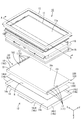
- FIG. 1 is an exploded perspective view showing a schematic configuration of a television receiver according to Embodiment 1 of the present invention.
- the exploded perspective view which shows schematic structure of the liquid crystal display device with which a television receiver is equipped
- Sectional drawing which shows the cross-sectional structure along the long side direction of a liquid crystal panel
- Enlarged plan view showing the planar configuration of the array substrate
- the top view which shows the arrangement
- Embodiment 1 of the present invention will be described with reference to FIGS.
- the lighting device 12, the liquid crystal display device 10 including the lighting device 12, and the television receiver TV including the liquid crystal display device 10 are illustrated.
- an X axis, a Y axis, and a Z axis are shown as appropriate.
- the upper side shown by FIG.2 and FIG.3 be a front side, and let the lower side be a back side.
- FIG. 1 is an exploded perspective view showing a schematic configuration of a television receiver TV according to Embodiment 1 of the present invention.
- the television receiver TV includes a liquid crystal display device 10, front and back cabinets Ca and Cb that are accommodated so as to sandwich the liquid crystal display device 10, a power source P, a tuner T, and a stand S. I have.
- the liquid crystal display device (display device) 10 has a horizontally long (longitudinal) rectangular shape as a whole, and is accommodated between the front and back cabinets Ca and Cb in a so-called vertical state.
- FIG. 2 is an exploded perspective view showing a schematic configuration of the liquid crystal display device 10 included in the television receiver TV.
- the liquid crystal display device 10 includes a liquid crystal panel 11 as a display panel, and a backlight device (illumination device) 12 as an external light source, which includes a frame-like bezel 13 and the like. It is held integrally using.
- FIG. 3 is a cross-sectional view showing a cross-sectional configuration along the long side direction of the liquid crystal panel 11.
- the liquid crystal panel 11 is made of a liquid crystal material, which is a substance whose optical characteristics change with application of an electric field, between a pair of transparent (translucent) glass substrates 20 and 21.
- the liquid crystal layer 22 containing it is enclosed.
- the two substrates 20 and 21 constituting the liquid crystal panel 11 the one arranged on the back side (backlight device 12 side) is an array substrate (TFT substrate, active matrix substrate) 20 and arranged on the front side (light emitting side).
- TFT substrate, active matrix substrate active matrix substrate
- What is to be processed is a CF (color filter) substrate (counter substrate) 21.
- a pair of front and back polarizing plates 23 are respectively attached to the outer surface sides of both the substrates 20 and 21.
- the liquid crystal panel 11 displays an image on the front surface (display surface) 11a.
- FIG. 4 is an enlarged plan view showing a planar configuration of the array substrate 20.
- a TFT Thin Film
- Transistors 24 and pixel electrodes 25 are arranged in a matrix (matrix shape) along the plate surface of the array substrate 20, and around the TFTs 24 and the pixel electrodes 25, gate wirings in a lattice shape are provided. 26 and the source wiring 27 are disposed so as to surround them.
- the pixel electrode 25 is made of a transparent conductive film such as ITO (Indium Tin Oxide).
- Both the gate wiring 26 and the source wiring 27 are made of a conductive material.
- the gate wiring 26 and the source wiring 27 are connected to the gate electrode 24a and the source electrode 24b of the TFT 24, respectively, and the pixel electrode 25 is connected to the drain electrode 24c of the TFT 24 via the drain wiring (not shown).
- the array substrate 20 is provided with a capacitor wiring (auxiliary capacitor wiring, storage capacitor wiring, Cs wiring) 33 that is arranged in parallel to the gate wiring 26 and overlaps the pixel electrode 25 in plan view.
- the capacitor wiring 33 is arranged alternately with the gate wiring 26 in the Y-axis direction.
- the gate wiring 26 is disposed between the pixel electrodes 25 adjacent to each other in the Y-axis direction, whereas the capacitor wiring 33 is disposed at a position that substantially crosses the central portion of each pixel electrode 25 in the Y-axis direction.
- the end portion of the array substrate 20 is provided with a terminal portion routed from the gate wiring 26 and the capacitor wiring 33 and a terminal portion routed from the source wiring 27.
- Each signal or reference potential is input from a panel control section provided on the control board that is not to be operated, and thereby the driving of the TFTs 24 arranged in parallel in a matrix is individually controlled.
- An alignment film 28 for aligning liquid crystal molecules included in the liquid crystal layer 22 is formed on the inner surface side of the array substrate 20 (see FIG. 3).
- FIG. 5 is an enlarged plan view showing a planar configuration of the CF substrate 21.
- the inner surface side (the liquid crystal layer 22 side, the surface facing the array substrate 20) of the CF substrate 21 is superimposed on each pixel electrode 25 on the array substrate 20 side in a plan view as shown in FIGS. 3 and 5.
- a large number of color filters 29 are arranged in a matrix along the plate surface of the CF substrate 21 at positions where the color filters 29 are arranged.
- the color filter 29 constitutes a colored portion group by alternately arranging the colored portions 29R, 29G, and 29B exhibiting red, green, and blue along the row direction (X-axis direction). Many arrangements are arranged along the direction (Y-axis direction).
- the coloring portions 29R, 29G, and 29B that constitute the color filter 29 selectively transmit light of each color (each wavelength).
- the outer shape of each of the colored portions 29R, 29G, and 29B has a vertically long rectangular shape as viewed in a plane following the outer shape of the pixel electrode 25.
- a light shielding portion (black matrix) 30 having a lattice shape for preventing color mixture is formed.
- the light shielding unit 30 is superimposed on the gate wiring 26, the source wiring 27, and the capacitor wiring 33 on the array substrate 20 side in plan view. Further, as shown in FIG.
- a counter electrode 31 that faces the pixel electrode 25 on the array substrate 20 side is provided on the surface of the color filter 29 and the light shielding portion 30.
- An alignment film 32 for aligning liquid crystal molecules contained in the liquid crystal layer 22 is formed on the inner surface side of the CF substrate 21.
- the liquid crystal panel 11 is a display unit by a set of three colored portions 29R, 29G, and 29B of three colors of R, G, and B and three pixel electrodes 25 facing them.
- One unit pixel PX is configured, and the unit pixels PX are arranged in parallel in a matrix form in large numbers along the plate surfaces of both the substrates 11a and 11b, that is, the display surfaces (X-axis direction and Y-axis direction). Yes. That is, the unit pixel PX includes a red pixel RPX having a red coloring portion 29R, a green pixel GPX having a green coloring portion 29G, and a blue pixel BPX having a blue coloring portion 29B.
- the red pixel RPX, the green pixel GPX, and the blue pixel BPX constituting the unit pixel PX are repeatedly arranged along the row direction (X-axis direction) to form a pixel group, and the pixel group is in the column direction Many are arranged along the (Y-axis direction).
- the panel controller controls the driving of the TFTs 24 included in the pixels RPX, GPX, and BPX, so that a predetermined voltage is applied between the pixel electrodes 25 connected to the TFTs 24 and the counter electrode 31. Then, the alignment state of the liquid crystal layer 22 disposed therebetween changes according to the voltage, and as a result, the amount of light transmitted through the colored portions 29R, 29G, and 29B of each color is individually controlled.
- the backlight device 12 includes a chassis 14 having a substantially box shape having a light emitting portion 14 c that opens on the front side (light emitting side, liquid crystal panel 11 side), and a light emitting portion of the chassis 14. 14c, an optical member 15, a frame 16 that holds a light guide plate 19 described below from the front side, a light source LED (Light Emitting Diode) 17, and an LED substrate on which the LED 17 is mounted (light source)
- An LED unit (light source unit) LU including a substrate 18, a light guide plate 19 that guides light from the LED 17 and guides the light to the optical member 15 (liquid crystal panel 11, light emission side), and the like.
- the backlight device 12 is configured such that one LED unit LU is arranged at each of the both ends on the short side, and light is incident from both end surfaces on the short side of the light guide plate 19. . That is, the backlight device 12 according to the present embodiment is an edge light type of both-side incident light type.
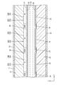
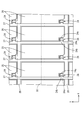
- FIG. 6 is a plan view showing a positional relationship among the chassis 14, the light guide plate 19 and the LED unit LU included in the backlight device 12, and
- FIG. 7 is a cross-sectional view taken along the line AA in FIG. 2.
- the chassis 14 is formed by processing a metal plate such as an aluminum plate or an electrogalvanized steel plate (SECC) into a shallow box shape. As shown in FIG. 2 and the like, the chassis 14 has a horizontally long bottom plate 14a and outer ends of each side (a pair of long sides and a pair of short sides) surrounding the bottom plate 14a, as in the liquid crystal panel 11. And a side plate 14b rising toward the front side.
- the pair of side plates 14b on the long side may be specifically referred to as side plates 14b1 and 14b2
- the pair of side plates 14b on the short side may be specifically referred to as side plates 14b3 and 14b4.
- the chassis 14 (bottom plate 14a) is shown in each drawing such that its long side direction coincides with the X-axis direction and its short side direction coincides with the Y-axis direction. Note that substrates such as a control board and an LED drive circuit board (not shown) are attached to the back side of the bottom plate 14a. Further, the side plate 14 b is configured to be screwed to the frame 16 and the bezel 13.
- the optical member 15 has a horizontally long rectangular shape as viewed from above, like the liquid crystal panel 11 and the chassis 14.
- the optical member 15 is accommodated in the backlight device 12 so as to be placed on the front side (light emitting side) of the light guide plate 19.
- the optical member 15 is interposed between the liquid crystal panel 11 and the light guide plate 19, and transmits the light emitted from the light guide plate 19 toward the liquid crystal panel 11. It has a function of imparting optical action.
- the optical member 15 is composed of a plurality of (three in the present embodiment) sheet-like members stacked on each other.
- Specific examples of the optical member (optical sheet) 15 include a diffusion sheet 15a, a lens sheet 15b, a reflective polarizing sheet 15c, and the like, and are appropriately selected from these.
- the frame 16 is formed in a frame shape (frame shape) extending substantially along the outer peripheral end of the light guide plate 19.
- the frame 16 is configured to hold the outer peripheral end portion of the light guide plate 19 from the front side over substantially the entire circumference.
- the frame 16 is made of a synthetic resin molded product or the like.
- the surface of the frame 16 has a light-shielding color such as black.
- the frame 16 is configured to be covered from the upper end side of the side plate 14 of the chassis 14 that houses the light guide plate 19 and the like.
- the frame 16 is configured to receive the outer peripheral end of the liquid crystal panel 11 from the back side.
- a pair of LED units LU (one set) are arranged in the backlight device 12 so as to face each other with the light guide plate 19 interposed therebetween.
- One LED unit LU is assigned to each of both ends on the short side of the light guide plate 19.
- the pair of LED units LU the one arranged on the side plate 14b3 side of the chassis 14 is particularly referred to as a first LED unit (first light source unit) LU1, and the one arranged on the side plate 14b4 side of the chassis 14 is particularly preferred. This is called a second LED unit (second light source unit) LU2.
- the first LED unit LU1 includes a first LED row (first light source row) 171 including a plurality of (four in the case of the present embodiment) LEDs 17 arranged in a row, and a longitudinal LED substrate 18.
- the LED substrate 18 included in the first LED unit LU1 is particularly referred to as a first substrate 181.
- the first substrate 181 has a plate shape (strip shape) elongated along the short side direction of the light guide plate 19, and includes a first mounting portion 181 a on which each LED 17 constituting the first LED row 171 is mounted, And a first non-mounting portion 181b adjacent to the mounting portion 181a.
- the second LED unit LU2 includes a second LED row (second light source row) 172 composed of a plurality of (four in the case of the present embodiment) LEDs 17 arranged in a row, and a long LED substrate 18.
- the LED substrate 18 provided in the second LED unit LU2 is particularly referred to as a second substrate 182.
- the second substrate 182 has a plate shape (strip shape) elongated along the short side direction of the light guide plate.
- the basic configurations of the first LED unit LU1 and the second LED unit LU2 are the same. However, as shown in FIG. 2, FIG. 7 and the like, the first LED unit LU1 and the second LED unit LU2 are mounted on the first LED unit LU1 although they are arranged facing each other across the light guide plate 19. Each LED 17 and each LED 17 mounted on the second LED unit LU2 do not face each other.
- each LED 17 (first LED row 171) of the first LED unit LU1 is mainly a portion of one light guide plate 19. Light is supplied to (the portion disposed on the side plate 14b1 side, the lower portion of the light guide plate 19 in FIG. 6), and each LED 17 (second LED row 172) of the second LED unit LU2 is mainly configured of the other light guide plate 19. Light is supplied to the portion (the portion disposed on the side plate 14b2 side, the upper portion of the light guide plate 19 in FIG. 6).
- the first mounting portion 181a of the first LED unit LU1 faces the second non-mounting portion 182b of the second LED unit LU2, and the second mounting portion 182a of the second LED unit LU2 is the first LED unit.
- the first LED unit LU1 and the second LED unit LU2 are fixed to the light guide plate 19 so as to face the first non-mounting portion 181b of LU1.
- the portions where the LEDs 17 are mounted that is, the first mounting portion 181a and the second mounting portion 182a
- each LED 17 (first LED row) 171 on the first LED unit LU1 side is in a state of being offset toward the side plate 14b1 side of the chassis 14, and each LED 17 (second LED row) 172 on the second LED unit LU2 side is the chassis. 14 side plates 14b2 side.
- the backlight device 12 of the present embodiment is an edge light type of both-side incident light type, it is set so that the light incident surfaces (light incident surface, light incident portion) of the light guide plate 19 do not overlap each other.
- the LEDs 17 forming the first LED row 171 of the first LED unit LU1 are arranged in a row on the first mounting portion 181a while maintaining an equal interval therebetween.
- the LEDs 17 forming the second LED row 172 of the second LED unit LU2 are also arranged in a row on the second mounting portion 182a while maintaining an equal interval therebetween.
- the interval (pitch) between the LEDs 17 in the first LED row 171 and the interval (pitch) between the LEDs 17 in the second LED row 172 are set to be the same.
- the interval between the first LED row 171 and the second LED row 172 is also set to be the same as the interval (pitch) between the LEDs 17 described above. That is, the LEDs 17 forming the first LED row 171 and the LEDs 17 forming the second LED 172 are arranged in the same direction along the short side direction of the light guide plate, although the light emission directions are different from each other. It has become.
- the lengths of the first substrate 181 and the second substrate 182 are set to be the same, and are substantially the same as the length of the short side of the light guide plate 19.
- the first substrate 181 is divided into two equal parts in the longitudinal direction (the short side direction of the light guide plate 19) into a first mounting part 181a and a first non-mounting part 181b.
- the second substrate 182 is equally divided into a second mounting portion 182a and a second non-mounting portion 182b in the longitudinal direction (the short side direction of the light guide plate 19).
- the first non-mounting portion 181b included in the first LED unit LU1 and the second non-mounting portion 182b included in the second LED unit LU2 are directly fixed to the end portions of the light guide plate 19, respectively. It has become.
- the LED 17 used in the LED unit LU is mounted on the surface of the LED substrate 18 and its light emitting surface 17a faces away from the LED substrate 18 side. It is a surface emitting type.
- the LED 17 mainly includes an LED element (LED chip, light emitting element) that is a light source, a sealing material (translucent resin material) that seals the LED element, and an LED element that is housed and a sealing material. It has a configuration including a case (container, housing) to be filled.
- the LED 17 of the present embodiment is configured to emit white light.
- the LED substrate 18 used in the LED unit LU has a long plate shape extending along the short side direction (Y-axis direction) of the light guide plate 19. .
- the LED substrate 18 is fixed to the light guide plate 19, and its plate surface is oriented along the Y-axis direction and the Z-axis direction (that is, the LED substrate 18 is orthogonal to the plate surfaces of the liquid crystal panel 11 and the light guide plate 19).
- the LED substrate 18 has the long side direction on the plate surface coincident with the Y-axis direction, the short side direction coincides with the Z-axis direction, and the thickness direction perpendicular to the plate surface coincides with the X-axis direction. Is shown in
- the LED substrate 18 includes portions on which the LEDs 17 are mounted (the first mounting portion 181a of the first LED unit LU1 and the second mounting portion 182a of the second LED unit LU2) on a part of each end face on the short side of the light guide plate 19. Opposite portions where the LED 17 is not mounted (the first non-mounting portion 181b of the first LED unit LU1 and the second non-mounting portion 182b of the second LED unit LU2) are the other end surfaces on the short side of the light guide plate 19 It is attached directly to the light guide plate 19 by being fixed in close contact with a part of the light guide plate 19. Each LED 17 mounted on the LED board 18 has an optical axis that substantially coincides with the X-axis direction (the long side direction of the light guide plate 19 and the X-axis direction).
- the LED substrate 18 is a single-sided mounting type in which only one side of the plate surface is a mounting surface.
- the mounting surface of the LED substrate 18 (the mounting surface 181a1 of the first mounting portion 181a, the mounting surface 182a1 of the second mounting portion 182a, FIG. 6), extending along the Y-axis direction, crossing each LED row (first LED row 171 and second LED row 172), and connecting adjacent LEDs 17 in series, a metal film (copper foil or the like)
- a wiring pattern (not shown) is formed.
- a backlight control unit provided on an LED drive circuit board (not shown) is electrically connected to a terminal portion formed at an end of the wiring pattern via a wiring member or the like, so that a backlight is obtained. Drive power from the control unit is supplied to each LED 17 of each LED unit LU.
- the base material constituting the LED substrate 18 is made of a metal plate material such as aluminum.
- the LED substrate 18 has the wiring pattern (not shown) formed on the surface of the base material via an insulating layer.
- insulating materials such as a synthetic resin and a ceramic, may be used as a material used for the base material of the LED board 18.
- Double-sided adhesive tape is affixed.
- the LED substrate 18 is affixed to the end surface of the light guide plate 19 using a double-sided adhesive tape.
- a double-sided adhesive tape is attached to the surface 181b1 of the first non-mounting portion 181b of the LED substrate 18 (that is, the first substrate 181) included in the first LED unit LU1 so as to cover the surface 181b1.
- the first LED unit LU1 is fixed to the light guide plate 19 by attaching the first non-mounting portion 181b to a part of one end surface on the short side of the light guide plate 19 via a double-sided adhesive tape.
- a double-sided adhesive tape is attached to the surface 182b1 of the second non-mounting portion 182b of the LED substrate 18 (that is, the second substrate 182) included in the second LED unit LU2 so as to cover the surface 182b1.
- the second LED unit LU2 is fixed to the light guide plate 19 by attaching the second non-mounting portion 182b to a part of the other end surface on the short side of the light guide plate 19 via a double-sided adhesive tape. That is, the first non-mounting portion 181b is a fixed portion (first fixed portion) for fixing the first LED unit LU1 to the light guide plate 19, and the second non-mounting portion 182b is the second LED unit LU2. This is a fixed part (second fixed part) for fixing the light to the light guide plate 19.
- the light guide plate 19 is a plate-like member made of a synthetic resin material (for example, acrylic resin) having a refractive index sufficiently higher than that of air and substantially transparent (exceeding translucency). As shown in FIGS. 2 and 6, the light guide plate 19 has a substantially horizontally long rectangular shape when seen in a plane, like the liquid crystal panel 11 and the bottom plate 14a of the chassis 14. In each drawing, the light guide plate 19 has a long side direction on the plate surface that matches the X-axis direction, a short side direction that matches the Y-axis direction, and a plate thickness direction that is orthogonal to the plate surface matches the Z-axis direction. Shown to be.
- a synthetic resin material for example, acrylic resin
- the light guide plate 19 is disposed in the chassis 14 at a position directly below the liquid crystal panel 11 and the optical member 15.
- Each end on the long side of the light guide plate 19 has a substantially straight shape, but each end on the short side of the light guide plate 19 has a shape that is partially cut away. There is no.
- the end portion 191 on the side to which the first LED unit LU1 is fixed has a shape in which the side plate 14b1 side of the chassis 14 is cut away, and is opposite to the side plate 14b1.
- the side plate 14b2 side on the side has a shape projecting outwardly (side plate 14b3 side) in a convex shape.
- the part of the end 191 that is notched is a first housing portion 191a that houses the first LED row 171 of the first LED unit LU1, and has a convex shape adjacent to the first housing portion 191a.
- the portion is a first fixing portion 191b to which the first non-mounting portion 181b of the first LED unit LU1 is fixed.
- the end 192 on the side where the second LED unit LU2 is fixed has a shape in which the side plate 14b1 side protrudes outwardly (side plate 14b4 side) in a convex shape.
- the side plate 14b2 side is cut out.
- the notched portion is a second housing portion 192a that houses the second LED row 172 of the second LED unit LU2, and a convex shape adjacent to the second housing portion 192a.
- the portion is a second fixing portion 192b to which the second non-mounting portion 182b of the second LED unit LU2 is fixed.
- the first storage portion 191 a and the second storage portion 192 a provided at each end portion on the short side of the light guide plate 19 are mutually in the long side direction of the light guide plate 19. In order not to overlap, it is a so-called alternate state.
- the light guide plate 19 introduces light emitted from the LED 17 along the X-axis direction from the respective end portions 191 and 192 on the short side, and propagates the light inside thereof (on the optical member 15 side (front side, light It has the function of rising from the plate surface and emitting from the plate surface.
- the surface facing the front side (the surface facing the liquid crystal panel 11 and the optical member 15) is configured to transmit internal light to the optical member as shown in FIGS. 15 and the light emission surface (light emission part) 19a which radiate
- the first housing portion 191a is formed, and the end surface facing each LED 17 forming the first LED row 171 is emitted from the LED 17 of the first LED unit LU1. It is a light incident surface (first light incident portion) 191c on which light is incident.
- the light incident surface 191c extends along the short side direction of the light guide plate 19, and has a shape along the Y-axis direction and the Z-axis direction. A slight gap (clearance) is provided between the light incident surface 191c and each LED 17 of the first LED row 171.
- the second housing portion 192a is formed, and the end surface facing each LED 17 forming the second LED row 172 is emitted from the LED 17 of the second LED unit LU2.
- a light incident surface (second light incident portion) 192c on which the incident light is incident is formed.
- the light incident surface 192c extends along the short side direction of the light guide plate 19, and has a shape along the Y-axis direction and the Z-axis direction.
- a slight gap (clearance) is provided between the light incident surface 192c and each LED 17 of the first LED row 171.
- the light guide plate 19 is provided with two light incident surfaces (first light incident portion and second light incident portion) 191c and 192c.
- the light incident surfaces 191c and 192c are provided on a pair of end portions 191 and 192 on the short side facing each other.
- the light incident surface 191c and the light incident surface 192c are provided on the light guide plate 19 so as not to overlap each other in the long side direction of the light guide plate 19 (optical axis direction of the LED 17).
- the light incident surfaces 191c and 192c are substantially orthogonal to the light emitting surface 19a.
- each end surface 19b1, 19b2 on the long side of the light guide plate 19 has a shape facing the side plates 14b1, 14b2 on the long side in the chassis 14, respectively.
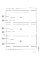
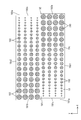
- a light reflection / scattering portion that reflects or scatters the light in the light guide plate 19 is provided on the plate surface (back surface) 19c on the opposite side of the light emitting surface 19a. It is patterned to have FIG. 8 is an explanatory diagram of the light reflection / scattering portion 193 formed on the back surface 19 c of the light guide plate 19.
- the light reflection / scattering portion 193 is formed of a coating film in which a paint containing a white pigment or the like is formed on a plate surface (back surface) 19c in a spot shape using a printing technique such as silk printing.
- the light reflection / scattering part 193 is set in a pattern so that the size of the spot increases in the long side direction of the light guide plate 19 away from the light incident surface 191c and approaching the second fixed part 192b.
- the light reflection / scattering portion 193 is set in a pattern so that the size of the spots increases in the long side direction of the light guide plate 19 away from the light incident surface 192c and approaching the first fixed portion 191b. ing. That is, in the vicinity of the light incident surfaces 191c and 192c with sufficient light, the pattern of the light reflection / scattering portion 193 is set small, and the light reflection / scattering portion is increased as the distance from the light incident surfaces 191c and 192c increases.
- the pattern 193 is set to be large.
- a light reflection / scattering portion by so-called embossing may be used.
- the reflection sheet R is arranged in the chassis 14 so as to cover the back surface (back surface) 19 c of the light guide plate 19.
- the reflection sheet R has a horizontally long rectangular shape, like the light guide plate 19 and the liquid crystal panel 11, and is accommodated in the chassis 14 so as to cover the bottom plate 14a.
- the reflection sheet R is made of, for example, a white foamable plastic sheet (foamable polyethylene terephthalate sheet).
- the reflection sheet R has a function of reflecting the light in the light guide plate 19 and raising it to the front side.
- the reflection sheet R is provided so as to cover the entire plate surface 19 c of the light guide plate 19. In the chassis 14, the reflection sheet R is sandwiched between the light guide plate 19 and the bottom plate 14 a.
- a plurality of rod-like locking pins are erected on the bottom plate 14 a of the chassis 14.
- the light guide plate 19 is provided with a plurality of locking holes (not shown) for inserting the locking pins from the back side (plate surface 19c side) to the front side (light emitting surface 19a side).
- the light guide plate 19 is positioned at a predetermined position in the chassis 14 by inserting a locking pin into the locking hole.
- the locking pin is provided at the center of the long side of the bottom plate 14 a, and the locking hole is provided at the center of the long side of the light guide plate 19.
- the reflection sheet R described above also includes a hole-shaped or notched locking portion for locking the locking pin, and is positioned in the chassis 14 using the locking pin. .
- the liquid crystal panel 11 is attached to the chassis 14 in a state of being sandwiched between the frame 16 provided in the backlight device 12 and the above-described bezel 13 covered from the front side of the frame 16.
- each LED 17 of each LED unit LU included in the backlight device (illumination device) 12 emits light (lights up).
- each LED 17 emits light
- light enters the light guide plate 19 from the light incident surfaces 191 c and 192 c of the light guide plate 19.
- the incident light is reflected and reflected by the reflection sheet R laid on the back side of the light guide plate 19 and the light reflection / scattering portion 193 formed on the back surface 19 c of the light guide plate 19, and proceeds in the light guide plate 19.
- the light is emitted from a light emission surface 19a formed of a front plate surface.
- the light emitted from the light emitting surface 19 a passes through the optical member 15 and becomes light spread in a planar shape, and illuminates the back surface 11 b of the liquid crystal panel 11. Then, the liquid crystal panel 11 uses the light from the backlight device 12 to display an image on the display surface 11a.
- the pair of LED units LU (the first LED unit LU1 and the second LED unit LU2) are directly fixed to the light guide plate 19, respectively. Therefore, if the pair of LED units LU is attached to the light guide plate 19 in advance, it can be assembled together with the light guide plate 19 at a predetermined location on the chassis 14.
- the distance (distance) between each light incident surface (first light incident part, second light incident part) 191c, 192c of the light guide plate 19 and each LED 17 of each LED unit LU. ) can be set to a predetermined value in advance.
- the distance between each LED 17 of the first LED unit LU1 and the light incident surface (first light incident portion) 191c is the length of the convex first fixing portion 191b at the end 191 of the light guide plate 19 (light incident surface). The length can be appropriately set by adjusting the length extending outward from 191c.
- the distance between each LED 17 of the second LED unit LU2 and the light incident surface (second light incident portion) 192c is the length of the convex second fixed portion 192b at the end 192 of the light guide plate 19 (light incident surface).
- the length can be appropriately set by adjusting the length extending outward from 192c.
- each LED unit LU is directly fixed to each end 191, 192 of the light guide plate 19.
- each LED unit LU also moves together with each end 191, 192. Therefore, even if the light guide plate 19 is expanded and contracted due to thermal expansion or the like, the light incident efficiency on each light incident surface 191c, 192c of the light guide plate 19 is suppressed from decreasing. Further, even if the light guide plate 19 is expanded or contracted due to thermal expansion or the like, it is also possible to prevent the respective light incident surfaces 191c and 192c and the respective LEDs 17 from being damaged due to the respective LEDs 17 coming into contact with the respective light incident surfaces 191c and 192c. Is done.
- the first LED unit LU1 uses the first non-mounting portion 181b
- the second LED unit LU2 uses the second non-mounting portion 182b, respectively
- the light guide plate 19 is used.
- each LED unit LU of the present embodiment uses each of the end portions 191 and 192 (specifically, the first fixing portion 191b and the second fixing portion) of the light guide plate 19 by using a portion where the LED 17 is not mounted. 192b), the light incident on the light incident surfaces 191c and 192c is not hindered by the fixing structure, and a decrease in light incident efficiency on the light incident surfaces 191c and 192c is suppressed. it can.
- the LEDs 17 constituting the first LED row 171 of the first LED unit LU1 can be arranged at a so-called narrow pitch interval. Therefore, when another member such as a support member is arranged between the adjacent LEDs 17, a portion where the light amount is partially insufficient (luminance unevenness) occurs in the light emitted from the backlight device 12. Is suppressed.
- the LEDs 17 are not mounted in a row in the longitudinal direction on each LED board 18 of each LED unit LU, but are mounted in a half portion in the longitudinal direction. The Therefore, the number of LEDs 17 to be mounted on one LED substrate 18 can be suppressed as compared with, for example, a case where the LEDs 17 are mounted in an overall row in the longitudinal direction. As a result, it becomes easy to stabilize lighting of the LEDs 17 connected in series with each other. And it becomes possible to narrow the space
- FIG. 9 is a plan view showing a positional relationship among the chassis 14A, the light guide plate 19A, and the LED units LU (LU1A, LU2A) included in the backlight device 12A according to the second embodiment.
- each structure corresponding to Embodiment 1 is represented by adding “A” to the reference numerals representing each structure of Embodiment 1, and description thereof will be omitted as appropriate.
- one LED unit (first LED unit LU1A, second LED unit LU2A) is provided at each end on the long side of the light guide plate 19A having a rectangular shape in plan view. It is attached. As in the present embodiment, the LED unit may be fixed to each end portion on the long side of the light guide plate 19A.
- FIG. 10 is a plan view illustrating a positional relationship among the chassis 14B, the light guide plate 19B, and the LED units included in the backlight device 12B according to the third embodiment.
- each structure corresponding to Embodiment 1 is represented by adding a sign “B” to the reference numerals representing each structure of Embodiment 1, and description thereof will be omitted as appropriate.
- two pairs (two sets) of LED units are used so as to sandwich the light guide plate 19B in the long side direction and the short side direction, respectively.
- a pair of LED units (first LED unit LU1B and second LED unit LU2B) arranged at each end on the short side of the light guide plate 19B, and each end on the long side of the light guide plate 19B.
- a pair of LED units (a third LED unit LU3B and a fourth LED unit LU4B).
- two or more sets of LED units may be used. In that case, it is preferable to set so that LED17B of each LED unit may not mutually adjoin between the long side of the adjacent light-guide plate 19B like this embodiment.
- the luminance of the portion may become higher than necessary.
- the light incident surface (light incident portion) on the long side of the light guide plate 19B and the light incident surface (light incident portion) on the short side are not adjacent to each other.
- FIG. 11 is a plan view illustrating a positional relationship among the chassis 14C, the light guide plate 19C, and the LED units included in the backlight device 12C according to the fourth embodiment.
- each component corresponding to the first embodiment is represented by adding a symbol “C” to the symbols representing the components of the first embodiment, and the description thereof will be omitted as appropriate.
- the backlight device 12C of the present embodiment includes a pair of LED units LU1C and LU2C that are arranged to face each other with the light guide plate 19C interposed therebetween, as in the first embodiment.
- the LED units LU1C and LU2C are assigned to the end portions 191C and 192C on the short side of the light guide plate 19C, respectively.
- the end portions 191C and 192C to which the LED units LU1C and LU2C are attached have a flat shape.
- the first fixed portion 191b does not protrude outwardly. That is, the light guide plate 19C has a horizontally long rectangular shape in plan view.
- the light incident surface (first light incident portion) 191Cc at the end 191C of the light guide plate 19C is adjacent to the first fixing portion 191Cb, and the light incident surface 191Cc and the surface of the first fixing portion 191Cb are the same. It is arranged on a plane.
- the light incident surface (second light incident portion) 192Cc at the end 192C of the light guide plate 19C and the second fixing portion 192Cb are adjacent to each other, and the light incident surface 192Cc and the surface of the second fixing portion 192Cb are the same. It is arranged on a plane.
- the backlight device 12C of the present embodiment includes each non-mounting portion (first non-mounting portion 181Cb and second non-mounting portion 182Cb) of each LED unit LU1C, LU2C.
- the thickness is set larger than each mounting part (first mounting part 181Ca and second mounting part 182Ca).
- each non-mounting part has the shape which protruded convexly to the light-guide plate 19C side rather than LED17C mounted in each mounting part (1st mounting part 181Ca and 2nd mounting part 182Ca).
- the first non-mounting portion 181Cb of the first LED unit LU1C is thicker than the first mounting portion 181Ca, and more convex than each LED 17C mounted on the first mounting portion 181C. It has a raised shape.
- the first LED unit LU1C is fixed to the light guide plate 19C in such a manner that the first non-mounting portion 181Cb is attached to the first fixing portion 191Cb via a double-sided adhesive tape.
- the second non-mounting portion 182Cb of the second LED unit LU2C is thicker than the second mounting portion 182Ca, and has a shape that rises more convex than each LED 17C mounted on the second mounting portion 182Ca. There is no.
- the second LED unit LU2C is fixed to the light guide plate 19C in such a manner that the second non-mounting portion 182Cb is attached to the second fixing portion 192Cb via a double-sided adhesive tape.
- the LED unit side is provided with raised portions (first non-mounting portion 181Cb and second non-mounting portion 182Cb), and each LED 17C of the LED unit is guided to the LED unit.
- interval (gap) between each light-incidence surface 191Cc and 192Cc of the optical plate 19C may be sufficient.
- the number of LEDs 17 forming the first LED row 171 of the first LED unit LU1 and the number of LEDs forming the second LED row 172 of the second LED unit LU2 are the same.
- the forms may be different from each other.
- each LED unit LU is fixed to the light guide plate 19 using a double-sided adhesive tape.
- a fixing means such as a screw is used. It may be fixed.
- a double-sided adhesive tape you may use the thing provided with the light reflectivity.
- each LED unit LU may be attached to the light guide plate 19 in a state where a slight gap is formed instead of being in close contact with the light guide plate 19 as long as the object of the present invention can be achieved. However, in consideration of light incident efficiency and the like, it is preferable that each LED unit LU is in close contact with the light guide plate 19.
- the first mounting portion 181a of the first LED unit LU and the second mounting portion 182a of the second LED unit LU do not overlap each other in the longitudinal direction of the light guide plate 19.
- the first mounting portion 181a and the second mounting portion 182a may partially overlap each other. That is, in the center of the light guide plate 19, there may be a portion where the light supplied from the first LED unit LU1 and the light supplied from the second LED unit LU2 overlap each other.
- the first LED unit LU1 and the second LED unit LU2 may be arranged as described above.
- a TFT is used as a switching element of a liquid crystal display device.
- the present invention can also be applied to a liquid crystal display device using a switching element other than TFT (for example, a thin film diode (TFD)).
- a switching element other than TFT for example, a thin film diode (TFD)
- the present invention can also be applied to a liquid crystal display device for monochrome display.
- the television receiver provided with the tuner is exemplified, but the present invention can also be applied to a display device not provided with the tuner. Specifically, the present invention can also be applied to a liquid crystal display device used as an electronic signboard (digital signage) or an electronic blackboard.
- DESCRIPTION OF SYMBOLS 10 ... Liquid crystal display device (display device), 11 ... Liquid crystal panel (display panel), 12 ... Backlight device (illumination device), 13 ... Bezel, 14 ... Chassis, 15 ... Optical member, 16 ... Frame, 17 ... LED ( Light source), 171 ... first LED row (first light source row), 172 ... second LED row (second light source row), 18 ... LED substrate (light source substrate), 181 ... first substrate, 181a ... first mounting portion, 181b ... 1st non-mounting part, 182 ... 2nd board
Landscapes
- Physics & Mathematics (AREA)
- General Physics & Mathematics (AREA)
- Optics & Photonics (AREA)
- Chemical & Material Sciences (AREA)
- Crystallography & Structural Chemistry (AREA)
- Engineering & Computer Science (AREA)
- Multimedia (AREA)
- Signal Processing (AREA)
- Planar Illumination Modules (AREA)
Abstract
Description
特許文献1に示されるように、一対のLED光源が導光板を挟んで互いに向かい合う形で配されている場合、部品の組立公差等を考慮すると、一方のLED光源のみが配されている場合と比べて、光入射面とLED光源との間の隙間を広めに設計する必要がある。そのため、このような構成の照明装置では、光入射面に対する入光効率が低下してしまうことが問題となっていた。
本発明に係る照明装置は、列状に並ぶ複数の光源からなる第1光源列と、前記第1光源列をなす各光源が実装される第1実装部、及び前記第1実装部に隣接する第1非実装部を含む長手状の第1基板とを有する第1光源ユニットと、列状に並ぶ複数の光源からなる第2光源列と、前記第2光源列をなす各光源が実装される第2実装部、及び前記第2実装部に隣接する第2非実装部を含む長手状の第2基板とを有する第2光源ユニットと、板状部材であって、前記板状部材の一端に設けられ前記第1光源列をなす各光源からの光が入射される第1光入射部と、前記第1光入射部に隣接する形で前記一端に設けられ前記第1非実装部に密着する形で前記第1光源ユニットを固定する第1固定部と、前記一端の反対側にある前記板状部材の他端に前記1固定部と重なる形で設けられ前記第2光源列をなす各光源からの光が入射される第2光入射部と、前記第2入射部に隣接しつつ前記第1光入射部と重なる形で設けられ前記第2非実装部に密着する形で前記第2光源ユニットを固定する第2固定部と、前記板状部材の板面からなり前記第1光入射部及び前記第2光入射部から入射された光を出射する光出射部とを有する導光板と、を備える。
本発明によれば、導光板を挟んで互いに向かい合う形で配されている一対の光源ユニットを備える照明装置において、導光板に対する入光効率の低下を抑制する技術を提供することができる。
本発明の実施形態1を図1から図8を参照しつつ説明する。本実施形態では、照明装置12と、この照明装置12を備える液晶表示装置10と、この液晶表示装置10を備えるテレビ受信装置TVについて例示する。なお、各図面には、適宜、X軸、Y軸及びZ軸が示されている。また、図2及び図3に示される上側を表側とし、下側を裏側とする。
次いで、本発明の実施形態2を、図9を参照しつつ説明する。図9は、実施形態2に係るバックライト装置12Aが備えるシャーシ14A、導光板19A及びLEDユニットLU(LU1A,LU2A)の配置関係を示す平面図である。なお、本実施形態において、実施形態1と対応する各構成は、実施形態1の各構成を表す符号に、更に符号「A」を追加して表し、適宜、説明を省略する。
次いで、本発明の実施形態3を、図10を参照しつつ説明する。図10は、実施形態3に係るバックライト装置12Bが備えるシャーシ14B、導光板19B及びLEDユニットの配置関係を示す平面図である。なお、本実施形態において、実施形態1と対応する各構成は、実施形態1の各構成を表す符号に、更に符号「B」を追加等して表し、適宜、説明を省略する。本実施形態では、導光板19Bを、長辺方向及び短辺方向においてそれぞれ挟むように、二対(2組)のLEDユニットが利用される。具体的には、導光板19Bの短辺側の各端部に配される一対のLEDユニット(第1LEDユニットLU1B、及び第2LEDユニットLU2B)と、導光板19Bの長辺側の各端部に配される一対のLEDユニット(第3LEDユニットLU3B、及び第4LEDユニットLU4B)とを備えている。本実施形態のバックライト装置12Bのように、2組以上のLEDユニットを利用してもよい。その場合、本実施形態のように、隣り合った導光板19Bの長辺と短辺との間において、各LEDユニットのLED17B同士が互いに隣接しないように設定されることが好ましい。隣り合った導光板19Bの長辺と短辺との間において、各LEDユニットのLED17B同士が互いに隣接すると、その部分の輝度が必要以上に高くなってしまう虞があるからである。要するに、導光板19Bの長辺側の光入射面(光入射部)と、短辺側の光入射面(光入射部)とが互いに隣接しないように設定されることが好ましい。
次いで、本発明の実施形態4を、図11を参照しつつ説明する。図11は、実施形態4に係るバックライト装置12Cが備えるシャーシ14C、導光板19C及びLEDユニットの配置関係を示す平面図である。なお、本実施形態において、実施形態1と対応する各構成は、実施形態1の各構成を表す符号に、更に符号「C」を追加等して表し、適宜、説明を省略する。
本発明は上記記述及び図面によって説明した実施形態に限定されるものではなく、例えば次のような実施形態も本発明の技術的範囲に含まれる。
Claims (10)
- 列状に並ぶ複数の光源からなる第1光源列と、前記第1光源列をなす各光源が実装される第1実装部、及び前記第1実装部に隣接する第1非実装部を含む長手状の第1基板とを有する第1光源ユニットと、
列状に並ぶ複数の光源からなる第2光源列と、前記第2光源列をなす各光源が実装される第2実装部、及び前記第2実装部に隣接する第2非実装部を含む長手状の第2基板とを有する第2光源ユニットと、
板状部材であって、前記板状部材の一端に設けられ前記第1光源列をなす各光源からの光が入射される第1光入射部と、前記第1光入射部に隣接する形で前記一端に設けられ前記第1非実装部に密着する形で前記第1光源ユニットを固定する第1固定部と、前記一端の反対側にある前記板状部材の他端に前記1固定部と重なる形で設けられ前記第2光源列をなす各光源からの光が入射される第2光入射部と、前記第2入射部に隣接しつつ前記第1光入射部と重なる形で設けられ前記第2非実装部に密着する形で前記第2光源ユニットを固定する第2固定部と、前記板状部材の板面からなり前記第1光入射部及び前記第2光入射部から入射された光を出射する光出射部とを有する導光板と、を備える照明装置。 - 前記導光板は、前記第1固定部が前記第1光入射部よりも外側に凸状に張り出した形をなし、前記第2固定部が前記第2光入射部よりも外側に凸状に張り出した形をなす請求項1に記載の照明装置。
- 前記第1基板は、前記光源が実装される前記第1実装部の表面と、前記第1固定部に密着される前記第1非実装部の表面とが同一平面上に配される形をなし、
前記第2基板は、前記光源が実装される前記第2実装部の表面と、前記第2固定部に密着される前記第2非実装部の表面とが同一面上に配される形をなす請求項2に記載の照明装置。 - 前記第1基板は、前記第1非実装部が、前記第1実装部に実装されている前記光源よりも凸状に盛り上がった形をなし、
前記第2基板は、前記第2非実装部が、前記第2実装部に実装されている前記光源よりも凸状に盛り上がった形をなす請求項1に記載の照明装置。 - 前記導光板は、前記第1光源列をなす各光源と対向する前記第1光入射部の表面と、前記第1非実装部と密着する前記第1固定部の表面とが同一平面上に配される形をなし、かつ前記第2光源列をなす各光源と対向する前記第2光入射部の表面と、前記第2非実装部と密着する前記第2固定部の表面とが同一平面上に配される形をなす請求項4に記載の照明装置。
- 前記第1光源ユニットは、前記第1非実装部が前記第1固定部に対して両面接着テープを介して貼り付けられる形で、前記導光板に固定され、
前記第2光源ユニットは、前記第2非実装部が前記第2固定部に対して両面接着テープを介して貼り付けられる形で、前記導光板に固定される請求項1から5の何れか一項に記載の照明装置。 - 前記第1光源列をなす光源同士の間隔と、前記第2光源列をなす光源同士の間隔とが、同じに設定されている請求項1から6の何れか一項に記載の照明装置。
- 請求項1から請求項7のいずれか一項に記載の照明装置と、前記照明装置からの光を利用して表示を行う表示パネルとを備える表示装置。
- 前記表示パネルは、一対の基板間に液晶を封入してなる液晶パネルからなる請求項8に記載の表示装置。
- 請求項8又は請求項9に記載された表示装置を備えるテレビ受信装置。
Priority Applications (2)
| Application Number | Priority Date | Filing Date | Title |
|---|---|---|---|
| CN201480014255.1A CN105190154B (zh) | 2013-04-25 | 2014-02-25 | 照明装置、显示装置以及电视接收装置 |
| US14/780,020 US9482813B2 (en) | 2013-04-25 | 2014-02-25 | Lighting device, display device and television device |
Applications Claiming Priority (2)
| Application Number | Priority Date | Filing Date | Title |
|---|---|---|---|
| JP2013092384 | 2013-04-25 | ||
| JP2013-092384 | 2013-04-25 |
Publications (1)
| Publication Number | Publication Date |
|---|---|
| WO2014174885A1 true WO2014174885A1 (ja) | 2014-10-30 |
Family
ID=51791470
Family Applications (1)
| Application Number | Title | Priority Date | Filing Date |
|---|---|---|---|
| PCT/JP2014/054450 Ceased WO2014174885A1 (ja) | 2013-04-25 | 2014-02-25 | 照明装置、表示装置及びテレビ受信装置 |
Country Status (3)
| Country | Link |
|---|---|
| US (1) | US9482813B2 (ja) |
| CN (1) | CN105190154B (ja) |
| WO (1) | WO2014174885A1 (ja) |
Cited By (1)
| Publication number | Priority date | Publication date | Assignee | Title |
|---|---|---|---|---|
| US9904108B2 (en) | 2015-05-26 | 2018-02-27 | Lg Display Co., Ltd. | Liquid crystal display with multiple display areas |
Families Citing this family (4)
| Publication number | Priority date | Publication date | Assignee | Title |
|---|---|---|---|---|
| CN106782349B (zh) * | 2017-01-04 | 2019-01-22 | 深圳市华星光电技术有限公司 | 一种led背光驱动电路及液晶显示器 |
| CN106773313A (zh) * | 2017-01-10 | 2017-05-31 | 友达光电(厦门)有限公司 | 背光模块 |
| JP2019067593A (ja) * | 2017-09-29 | 2019-04-25 | シャープ株式会社 | 照明装置及び表示装置 |
| JP2019139996A (ja) * | 2018-02-13 | 2019-08-22 | シャープ株式会社 | 照明装置 |
Citations (3)
| Publication number | Priority date | Publication date | Assignee | Title |
|---|---|---|---|---|
| JP2007019024A (ja) * | 2005-07-06 | 2007-01-25 | Samsung Electro Mech Co Ltd | Led光源が導光板に挿入されたバックライト装置の光源−導光板構造およびこれを含むバックライト装置 |
| JP2010114028A (ja) * | 2008-11-10 | 2010-05-20 | Panasonic Electric Works Co Ltd | 誘導灯装置および誘導灯器具 |
| JP2011232607A (ja) * | 2010-04-28 | 2011-11-17 | Funai Electric Co Ltd | 液晶モジュール |
Family Cites Families (4)
| Publication number | Priority date | Publication date | Assignee | Title |
|---|---|---|---|---|
| JP5295523B2 (ja) * | 2007-05-30 | 2013-09-18 | 株式会社ジャパンディスプレイ | 液晶表示装置 |
| TWM410895U (en) * | 2010-09-30 | 2011-09-01 | Chunghwa Picture Tubes Ltd | Backlight module |
| JP2012220689A (ja) | 2011-04-07 | 2012-11-12 | Sharp Corp | バックライト装置および液晶表示装置 |
| JP2012237826A (ja) * | 2011-05-10 | 2012-12-06 | Funai Electric Co Ltd | 液晶モジュール |
-
2014
- 2014-02-25 WO PCT/JP2014/054450 patent/WO2014174885A1/ja not_active Ceased
- 2014-02-25 US US14/780,020 patent/US9482813B2/en not_active Expired - Fee Related
- 2014-02-25 CN CN201480014255.1A patent/CN105190154B/zh not_active Expired - Fee Related
Patent Citations (3)
| Publication number | Priority date | Publication date | Assignee | Title |
|---|---|---|---|---|
| JP2007019024A (ja) * | 2005-07-06 | 2007-01-25 | Samsung Electro Mech Co Ltd | Led光源が導光板に挿入されたバックライト装置の光源−導光板構造およびこれを含むバックライト装置 |
| JP2010114028A (ja) * | 2008-11-10 | 2010-05-20 | Panasonic Electric Works Co Ltd | 誘導灯装置および誘導灯器具 |
| JP2011232607A (ja) * | 2010-04-28 | 2011-11-17 | Funai Electric Co Ltd | 液晶モジュール |
Cited By (2)
| Publication number | Priority date | Publication date | Assignee | Title |
|---|---|---|---|---|
| US9904108B2 (en) | 2015-05-26 | 2018-02-27 | Lg Display Co., Ltd. | Liquid crystal display with multiple display areas |
| TWI637214B (zh) * | 2015-05-26 | 2018-10-01 | 南韓商樂金顯示科技股份有限公司 | 具有多個顯示區域之液晶顯示器 |
Also Published As
| Publication number | Publication date |
|---|---|
| US20160033716A1 (en) | 2016-02-04 |
| CN105190154B (zh) | 2017-04-12 |
| CN105190154A (zh) | 2015-12-23 |
| US9482813B2 (en) | 2016-11-01 |
Similar Documents
| Publication | Publication Date | Title |
|---|---|---|
| US20160381317A1 (en) | Display device and television receiving device | |
| KR20100109785A (ko) | 액정표시장치 | |
| KR20110052069A (ko) | 백라이트 유닛 및 이를 포함하는 액정표시장치 | |
| KR20100078296A (ko) | 액정표시장치모듈 | |
| US8441597B2 (en) | Liquid crystal display device for preventing light leakage | |
| WO2013121998A1 (ja) | 照明装置、表示装置、及びテレビ受信装置 | |
| KR20100120407A (ko) | 액정표시장치 | |
| CN105209818A (zh) | 照明装置和显示装置 | |
| CN103998979B (zh) | 显示装置和电视接收装置 | |
| WO2013115084A1 (ja) | 表示装置、及びテレビ受信装置 | |
| US9304345B2 (en) | Liquid crystal display device | |
| WO2012133888A1 (ja) | 照明装置、表示装置、及びテレビ受信装置 | |
| CN105190154B (zh) | 照明装置、显示装置以及电视接收装置 | |
| JP5662952B2 (ja) | 照明装置、表示装置、及びテレビ受信装置 | |
| CN107532785A (zh) | 照明装置、显示装置、以及电视接收装置 | |
| WO2012165282A1 (ja) | 照明装置、表示装置、及びテレビ受信装置 | |
| WO2011092953A1 (ja) | 照明装置、表示装置、及びテレビ受信装置 | |
| US20150103258A1 (en) | Lighting device, display device and television device | |
| KR20130126407A (ko) | 액정표시장치 | |
| JP5368586B2 (ja) | 照明装置、表示装置、テレビ受信装置 | |
| US20160131828A1 (en) | Illumination device, display device, and tv receiver | |
| US10860277B2 (en) | Coupled display device | |
| WO2018066513A1 (ja) | 表示装置 | |
| WO2012077562A1 (ja) | 照明装置、表示装置及びテレビ受信装置 | |
| KR101785340B1 (ko) | 커버버툼 및 이를 포함하는 액정표시장치 |
Legal Events
| Date | Code | Title | Description |
|---|---|---|---|
| WWE | Wipo information: entry into national phase |
Ref document number: 201480014255.1 Country of ref document: CN |
|
| 121 | Ep: the epo has been informed by wipo that ep was designated in this application |
Ref document number: 14789096 Country of ref document: EP Kind code of ref document: A1 |
|
| WWE | Wipo information: entry into national phase |
Ref document number: 14780020 Country of ref document: US |
|
| NENP | Non-entry into the national phase |
Ref country code: DE |
|
| 122 | Ep: pct application non-entry in european phase |
Ref document number: 14789096 Country of ref document: EP Kind code of ref document: A1 |
|
| NENP | Non-entry into the national phase |
Ref country code: JP |