WO2014157281A1 - 配線基板 - Google Patents
配線基板 Download PDFInfo
- Publication number
- WO2014157281A1 WO2014157281A1 PCT/JP2014/058426 JP2014058426W WO2014157281A1 WO 2014157281 A1 WO2014157281 A1 WO 2014157281A1 JP 2014058426 W JP2014058426 W JP 2014058426W WO 2014157281 A1 WO2014157281 A1 WO 2014157281A1
- Authority
- WO
- WIPO (PCT)
- Prior art keywords
- acrylate
- meth
- wiring board
- pulse signal
- component
- Prior art date
- Legal status (The legal status is an assumption and is not a legal conclusion. Google has not performed a legal analysis and makes no representation as to the accuracy of the status listed.)
- Ceased
Links
Images




Classifications
-
- C—CHEMISTRY; METALLURGY
- C09—DYES; PAINTS; POLISHES; NATURAL RESINS; ADHESIVES; COMPOSITIONS NOT OTHERWISE PROVIDED FOR; APPLICATIONS OF MATERIALS NOT OTHERWISE PROVIDED FOR
- C09J—ADHESIVES; NON-MECHANICAL ASPECTS OF ADHESIVE PROCESSES IN GENERAL; ADHESIVE PROCESSES NOT PROVIDED FOR ELSEWHERE; USE OF MATERIALS AS ADHESIVES
- C09J133/00—Adhesives based on homopolymers or copolymers of compounds having one or more unsaturated aliphatic radicals, each having only one carbon-to-carbon double bond, and at least one being terminated by only one carboxyl radical, or of salts, anhydrides, esters, amides, imides, or nitriles thereof; Adhesives based on derivatives of such polymers
- C09J133/04—Homopolymers or copolymers of esters
- C09J133/06—Homopolymers or copolymers of esters of esters containing only carbon, hydrogen and oxygen, the oxygen atom being present only as part of the carboxyl radical
- C09J133/10—Homopolymers or copolymers of methacrylic acid esters
-
- G—PHYSICS
- G06—COMPUTING OR CALCULATING; COUNTING
- G06F—ELECTRIC DIGITAL DATA PROCESSING
- G06F3/00—Input arrangements for transferring data to be processed into a form capable of being handled by the computer; Output arrangements for transferring data from processing unit to output unit, e.g. interface arrangements
- G06F3/01—Input arrangements or combined input and output arrangements for interaction between user and computer
- G06F3/03—Arrangements for converting the position or the displacement of a member into a coded form
- G06F3/041—Digitisers, e.g. for touch screens or touch pads, characterised by the transducing means
- G06F3/0416—Control or interface arrangements specially adapted for digitisers
- G06F3/04164—Connections between sensors and controllers, e.g. routing lines between electrodes and connection pads
-
- G—PHYSICS
- G06—COMPUTING OR CALCULATING; COUNTING
- G06F—ELECTRIC DIGITAL DATA PROCESSING
- G06F3/00—Input arrangements for transferring data to be processed into a form capable of being handled by the computer; Output arrangements for transferring data from processing unit to output unit, e.g. interface arrangements
- G06F3/01—Input arrangements or combined input and output arrangements for interaction between user and computer
- G06F3/03—Arrangements for converting the position or the displacement of a member into a coded form
- G06F3/041—Digitisers, e.g. for touch screens or touch pads, characterised by the transducing means
- G06F3/044—Digitisers, e.g. for touch screens or touch pads, characterised by the transducing means by capacitive means
- G06F3/0445—Digitisers, e.g. for touch screens or touch pads, characterised by the transducing means by capacitive means using two or more layers of sensing electrodes, e.g. using two layers of electrodes separated by a dielectric layer
-
- G—PHYSICS
- G06—COMPUTING OR CALCULATING; COUNTING
- G06F—ELECTRIC DIGITAL DATA PROCESSING
- G06F3/00—Input arrangements for transferring data to be processed into a form capable of being handled by the computer; Output arrangements for transferring data from processing unit to output unit, e.g. interface arrangements
- G06F3/01—Input arrangements or combined input and output arrangements for interaction between user and computer
- G06F3/03—Arrangements for converting the position or the displacement of a member into a coded form
- G06F3/041—Digitisers, e.g. for touch screens or touch pads, characterised by the transducing means
- G06F3/044—Digitisers, e.g. for touch screens or touch pads, characterised by the transducing means by capacitive means
- G06F3/0446—Digitisers, e.g. for touch screens or touch pads, characterised by the transducing means by capacitive means using a grid-like structure of electrodes in at least two directions, e.g. using row and column electrodes
-
- H—ELECTRICITY
- H05—ELECTRIC TECHNIQUES NOT OTHERWISE PROVIDED FOR
- H05K—PRINTED CIRCUITS; CASINGS OR CONSTRUCTIONAL DETAILS OF ELECTRIC APPARATUS; MANUFACTURE OF ASSEMBLAGES OF ELECTRICAL COMPONENTS
- H05K2201/00—Indexing scheme relating to printed circuits covered by H05K1/00
- H05K2201/07—Electric details
- H05K2201/0753—Insulation
- H05K2201/0769—Anti metal-migration, e.g. avoiding tin whisker growth
-
- H—ELECTRICITY
- H05—ELECTRIC TECHNIQUES NOT OTHERWISE PROVIDED FOR
- H05K—PRINTED CIRCUITS; CASINGS OR CONSTRUCTIONAL DETAILS OF ELECTRIC APPARATUS; MANUFACTURE OF ASSEMBLAGES OF ELECTRICAL COMPONENTS
- H05K3/00—Apparatus or processes for manufacturing printed circuits
- H05K3/22—Secondary treatment of printed circuits
- H05K3/28—Applying non-metallic protective coatings
Definitions
- the present invention relates to a wiring board, and more particularly, to a wiring board considering ion migration between wirings.
- Japanese Patent Publication No. 2011-501767 discloses a transparent conductive wiring when stored for 30 to 40 days in a predetermined environment (temperature 60 ° C., relative humidity 90%) by selecting a constituent material of the transparent adhesive. Examples in which the increase in the surface resistance of the sheet is suppressed are described.
- JP 2011-501767 discloses a combination of a transparent conductive wiring and a transparent adhesive as described above.
- the purpose is to suppress a change in resistance of the transparent conductive wiring when stored for a long time in a predetermined environment.
- miniaturization of metal extraction wiring due to miniaturization or the like has progressed, and this is insufficient to suppress disconnection due to ion migration between metal wirings and short circuit between wirings.
- the present invention has been made in consideration of such problems, and an object thereof is to provide a wiring board having the following effects.
- A The potential difference between the metal extraction wirings can be effectively reduced.
- B Suppressing the occurrence of ion migration between metal extraction wires made of silver, copper, or the like.
- C It is possible to further promote downsizing, miniaturization of wiring, and narrowing between wirings.
- a wiring board according to the present invention is a wiring board having a plurality of metal wirings arranged on an insulating substrate and a transparent adhesive layer arranged on the metal wiring in direct contact with the metal wiring.
- the metal wiring is supplied with a first metal wiring to which the first pulse signal is supplied and a second pulse signal synchronized with the first pulse signal during a period in which the first pulse signal is supplied to the first metal wiring, And a second metal wiring to which a fixed potential is applied in other periods.
- a second pulse signal synchronized with the first pulse signal is supplied to the second metal wiring during a period in which the first pulse signal is supplied to the first metal wiring. Therefore, the potential difference between the first metal wiring and the second metal wiring can be reduced. Therefore, even if the first metal wiring and the second metal wiring are each composed of silver, copper, or the like, the occurrence of ion migration between the wirings can be suppressed.
- the metal wiring may contain silver and / or copper.
- each reference level of the first pulse signal and the second pulse signal is the same level as the fixed potential, and the absolute value of the amplitude of the first pulse signal and the absolute value of the amplitude of the second pulse signal are May be equal to or less than 1 ⁇ 2 of the absolute value of the amplitude of the first pulse signal.
- the first pulse signal and the second pulse signal may be the same pulse signal.
- the potential difference between the first metal wiring and the second metal wiring can be made substantially zero, and migration between the wirings can be prevented.
- the transparent pressure-sensitive adhesive layer has a transparent pressure-sensitive adhesive composed of at least one selected from the group consisting of the following optically transparent constituent component A, constituent component B, and constituent component C.
- the transparent adhesive is 100 parts
- the component A may contain 45 to 95 parts
- the component B may contain 20 to 50 parts
- the component C may contain 1 to 40 parts.
- Components A alkyl having a glass transition temperature T g of 25 ° C. or less (meth) acrylate monomer (wherein the alkyl group has 4 to 18 carbon atoms).
- Components B esters of (meth) acrylate monomer having a glass transition temperature T g of 25 ° C. or higher.
- Component C hydroxyalkyl (meth) acrylate, unsubstituted (meth) acrylamide, N-alkyl substituted (meth) acrylamide, N, N-dialkyl substituted (meth) acrylamide, monomer having urea functional group, lactam functional group, three A monomer selected from the group consisting of monomers having a primary amine, an alicyclic amine, an aromatic amine, and combinations thereof.
- the component A is at least one selected from the group consisting of n-butyl acrylate, 2-ethyl-hexyl (meth) acrylate, isooctyl acrylate, 2-methylhexyl acrylate, and combinations thereof. It may be.
- Component B may be at least one selected from the group consisting of methyl (meth) acrylate, ethyl (meth) acrylate, isobornyl (meth) acrylate, and combinations thereof.
- Component C is 2-hydroxyethyl (meth) acrylate, 3-hydroxypropyl (meth) acrylate, N-octylacrylamide, N, N-dimethylacrylamide, N, N-diethylacrylamide, vinylpyridine, vinylimidazole , N, N-dialkylaminoalkyl (meth) acrylate (wherein the alkyl group has 1 to 4 carbon atoms), and combinations thereof may be at least one selected from the group consisting of .
- component A is 2-ethyl-hexyl (meth) acrylate
- component B is isobornyl (meth) acrylate
- component C is 2-hydroxyethyl (meth) acrylate.
- the transparent adhesive contains 50 to 65 parts of 2-ethyl-hexyl (meth) acrylate as component A and 15 to 30 parts of isobornyl (meth) acrylate as component B.
- C preferably contains 20 to 30 parts of 2-hydroxyethyl (meth) acrylate.
- component A may be n-butyl acrylate and component C may be 2-hydroxyethyl (meth) acrylate. Also in this case, the whitening resistance performance of the transparent adhesive layer can be enhanced.
- the wiring board according to the present invention has the following effects.
- A The potential difference between the wirings can be effectively reduced.
- B The occurrence of ion migration between wirings made of silver, copper, or the like can be suppressed.
- C It is possible to further promote downsizing, miniaturization of wiring, and narrowing between wirings.
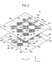
- FIG. 1 is an exploded perspective view showing a configuration example in which the wiring board according to the present embodiment is applied to a touch panel.
- FIG. 2 is an exploded perspective view showing a laminated conductive film (wiring board).
- FIG. 3 is an explanatory diagram illustrating an example of a cross-sectional structure of a laminated conductive film and an example of a control system (self-capacitance method).
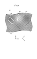
- FIG. 4 is a plan view showing a partially omitted example in which a laminated conductive film is formed by combining the first conductive film (wiring substrate) and the second conductive film (wiring substrate).
- FIG. 5 is an explanatory diagram showing a state in which one line is formed by the first auxiliary line and the second auxiliary line.
- FIG. 1 is an exploded perspective view showing a configuration example in which the wiring board according to the present embodiment is applied to a touch panel.
- FIG. 2 is an exploded perspective view showing a laminated conductive film (wiring board).
- FIG. 3
- FIG. 6 is a waveform diagram showing an example of signal waveforms of the first pulse signal to the fourth pulse signal.
- FIG. 7 is an explanatory diagram illustrating an example of a cross-sectional structure of a laminated conductive film and another example of a control system (self-capacitance method).
- FIG. 8 is an explanatory diagram showing an example of a cross-sectional structure of a laminated conductive film and an example of a control system (mutual capacitance method).
- FIG. 9 is an explanatory diagram illustrating an example of a cross-sectional structure of a laminated conductive film and another example of a control system (mutual capacitance method).
- FIG. 10 is an explanatory view showing another example of the cross-sectional structure of the laminated conductive film.
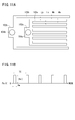
- FIG. 11A is an explanatory view showing a pattern example of the first metal wiring and the second metal wiring used in the first embodiment and the second embodiment, and FIG. 11B is applied to the first terminal of the first metal wiring. It is a wave form diagram which shows a pulse signal.
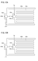
- FIG. 12A is an explanatory diagram showing a wiring state in Examples 1 to 17, and
- FIG. 12B is an explanatory diagram showing a wiring state in Comparative Examples 1 to 8.
- FIGS. 1 to 12B an embodiment in which the wiring board according to the present invention is applied to, for example, a touch panel will be described with reference to FIGS. 1 to 12B.
- ⁇ indicating a numerical range is used as a meaning including numerical values described before and after the numerical value as a lower limit value and an upper limit value.
- the touch panel 10 to which the wiring board according to the present embodiment is applied includes a sensor body 12 and a control circuit 14 (configured by an IC circuit or the like: see FIG. 3), as shown in FIG.
- the sensor body 12 includes a laminated conductive film 18 formed by laminating a first conductive film 16A (wiring board) and a second conductive film 16B (wiring board), and a protective layer 20 laminated thereon. And have.
- the laminated conductive film 18 and the protective layer 20 are arranged on a display panel 24 in a display device 22 such as a liquid crystal display.
- the first conductive film 16A and the second conductive film 16B include the first sensor unit 26A and the second sensor unit 26B arranged in a region corresponding to the display screen 24a of the display panel 24 when viewed from above. Have. Moreover, it has the 1st terminal wiring part 28A and the 2nd terminal wiring part 28B (what is called a frame) distribute
- the first sensor part 26A and the first terminal wiring part 28A constitute a first conductive part 30A
- the first conductive film 16A includes a first transparent base 32A, the above-described first conductive portion 30A formed on the surface of the first transparent base 32A, A first transparent pressure-sensitive adhesive layer 34A (see FIG. 3) formed so as to cover one conductive part 30A.
- the first sensor unit 26A includes a plurality of first conductive patterns 36A made of a transparent conductive layer composed of fine metal wires, and a plurality of first conductive patterns arranged around each first conductive pattern 36A.
- a first auxiliary pattern 38A configured by the auxiliary line 37A.
- the first conductive patterns 36A extend in the first direction (x direction) and are arranged in a second direction (y direction) orthogonal to the first direction.
- the first conductive pattern 36A is configured by connecting two or more first large lattices 40A in series in the first direction.
- Each first large lattice 40A is configured by combining two or more small lattices 42.
- the above-described first auxiliary pattern 38A that is not connected to the first large lattice 40A is formed around the side of the first large lattice 40A.
- first connection portions 44A for electrically connecting the first large lattices 40A are formed.
- a direction that bisects the first direction and the second direction is a third direction (m direction), and a direction orthogonal to the third direction is a fourth direction (n direction).
- the first connection portion 44A is configured by arranging a medium lattice 46 having a size in which p (p is a real number larger than 1) small lattices 42 are arranged in the fourth direction (n direction). .
- the small lattice 42 has the smallest square shape here.
- the medium lattice 46 has a size in which, for example, three small lattices 42 are arranged in one direction.
- the first conductive film 16 ⁇ / b> A configured as described above has an open end of the first large lattice 40 ⁇ / b> A existing on one end side of each first conductive pattern 36 ⁇ / b> A as a first connection.
- the portion 44A does not exist.
- the end portion of the first large lattice 40A existing on the other end portion side of each first conductive pattern 36A is electrically connected to the first terminal wiring pattern 50a made of metal wiring through the first connection portion 48a. .
- the first conductive film 16A applied to the touch panel 10 has the above-described multiple first conductive patterns 36A arranged in a portion corresponding to the first sensor unit 26A.
- a plurality of first terminal wiring patterns 50a (first metal wirings) derived from the first connection portions 48a are arranged.
- a first ground line for the purpose of shielding is provided so as to surround the first sensor portion 26A from one first ground terminal 52a to the other first ground terminal 52a.
- 54a (second metal wiring) is formed.
- the outer shape of the first conductive film 16A has a rectangular shape when viewed from above, and the outer shape of the first sensor portion 26A also has a rectangular shape.
- a peripheral portion on one long side of the first conductive film 16A is provided with a plurality of first ground terminals 52a in addition to the above-described pair of first grounding terminals 52a at the central portion in the length direction.
- the first connection terminals 56a are arranged in the length direction of the one long side.
- a plurality of first connection portions 48a are linearly arranged along one long side of the first sensor portion 26A (long side closest to one long side of the first conductive film 16A: y direction). Yes.
- the first terminal wiring pattern 50a derived from each first connection portion 48a is routed toward a substantially central portion on one long side of the first conductive film 16A, and is electrically connected to the corresponding first connection terminal 56a. Connected.
- the first transparent pressure-sensitive adhesive layer 34A formed so as to cover the first conductive portion 30A is a first terminal wiring pattern 50a (first metal wiring) of the first terminal wiring portion 28A.
- first metal wiring first metal wiring
- second metal wiring transparent conductive layer
- the second conductive film 16B includes a second transparent base 32B, the above-described second conductive portion 30B formed on the surface of the second transparent base 32B, And a second transparent adhesive layer 34B (see FIG. 3) formed to cover the two conductive portions 30B.
- the second sensor unit 26B includes a plurality of second conductive patterns 36B made of a transparent conductive layer formed of thin metal wires, and a plurality of second auxiliary lines 37B arranged around each second conductive pattern 36B. And a second auxiliary pattern 38B.
- the second conductive patterns 36B extend in the second direction (y direction) and are arranged in the first direction (x direction).
- the second conductive pattern 36B is configured by connecting two or more second large lattices 40B in series in the second direction.
- Each second large lattice 40B is also configured by combining two or more small lattices 42.
- the above-described second auxiliary pattern 38B that is not connected to the second large lattice 40B is formed around the side of the second large lattice 40B.
- second connection portions 44B that electrically connect the second large lattices 40B are formed.
- the second connection portion 44B is configured by arranging a medium lattice 46 having a size in which p small lattices 42 are arranged in the third direction (m direction).
- the open end of the second large lattice 40B existing on one end side of each second conductive pattern 36B has a shape in which the second connection portion 44B does not exist. It has become.
- the end portions of the large lattice 40B are electrically connected to the second terminal wiring pattern 50b made of metal wiring via the second connection portions 48b.
- the second conductive film 16B applied to the touch panel 10 has a large number of second conductive patterns 36B arranged at portions corresponding to the second sensor part 26B.
- a plurality of second terminal wiring patterns 50b (first metal wirings) derived from the respective second connection portions 48b are arranged.
- a second ground line for the purpose of shielding is provided so as to surround the second sensor portion 26B from one second ground terminal 52b to the other second ground terminal 52b.
- 54b second metal wiring
- a peripheral portion on one long side of the second conductive film 16B has a pair of the above-described second ground terminals at the central portion in the length direction.
- a plurality of second connection terminals 56b are arranged in the length direction of the one long side.
- a plurality of second connection portions 48b (for example, odd-numbered second lines) along one short side of the second sensor unit 26B (short side closest to one short side of the second conductive film 16B: x direction).
- the connecting portions 48b) are arranged in a straight line.
- a plurality of second connection portions 48b (for example, even-numbered second connection portions) along the other short side of the second sensor portion 26B (the short side closest to the other short side of the second conductive film 16B: the x direction). 48b) are arranged linearly.
- odd-numbered second conductive patterns 36B are connected to the corresponding odd-numbered second connection portions 48b.
- the even-numbered second conductive patterns 36B are connected to the corresponding even-numbered second connection portions 48b.
- the second terminal wiring patterns 50b derived from the odd-numbered and even-numbered second connection portions 48b are routed toward the substantially central portion on one long side of the second conductive film 16B, and the corresponding second terminals are connected. It is electrically connected to the connection terminal 56b.
- the first terminal wiring pattern 50a may be derived in the same manner as the second terminal wiring pattern 50b, and the second terminal wiring pattern 50b may be derived in the same manner as the first terminal wiring pattern 50a.
- the second transparent adhesive layer 34B formed so as to cover the second conductive portion 30B the second terminal wiring pattern 50b (first metal wiring) of the second terminal wiring portion 28B and the second ground line 54b.
- (2nd metal wiring) and 2nd conductive pattern 36B (transparent conductive layer) are contacted. And it arrange
- the thin metal wires constituting the first metal wiring, the second metal wiring, and the transparent conductive layer described above contain silver and / or copper, respectively.
- the length of one side of the first large lattice 40A and the second large lattice 40B is preferably 3 to 10 mm, and more preferably 4 to 6 mm. If the length of one side is less than the lower limit value, the capacitance of the first large grid 40A and the second large grid 40B at the time of detection is reduced, so that the possibility of detection failure increases. On the other hand, if the upper limit is exceeded, the position detection accuracy may be reduced. From the same viewpoint, the length of one side of the small lattice 42 constituting the first large lattice 40A and the second large lattice 40B is preferably 50 to 500 ⁇ m, and more preferably 150 to 300 ⁇ m. When the small lattice 42 is in the above range, it is possible to keep the transparency even better, and when it is mounted on the display panel 24 of the display device 22, the display can be visually recognized without a sense of incongruity.
- the line width of the first conductive pattern 36A (first large lattice 40A, medium lattice 46), the line width of the second conductive pattern 36B (second large lattice 40B, medium lattice 46), the first auxiliary pattern 38A (first The line widths of the auxiliary line 37A) and the second auxiliary pattern 38B (second auxiliary line 37B) are 1 to 9 ⁇ m, respectively.
- the line width of the first conductive pattern 36A and the line width of the second conductive pattern 36B may be the same or different.
- it is preferable that the line widths of the first conductive pattern 36A, the second conductive pattern 36B, the first auxiliary pattern 38A, and the second auxiliary pattern 38B are the same.
- the line width of the fine metal wire constituting the transparent conductive layer is preferably 1 ⁇ m or more, 3 ⁇ m or more, 4 ⁇ m or more, or 5 ⁇ m or more, and the upper limit is preferably 9 ⁇ m or less and 8 ⁇ m or less.
- the line width is less than the above lower limit value, the conductivity becomes insufficient, so that when used for a touch panel, the detection sensitivity becomes insufficient.
- the above upper limit is exceeded, moire becomes noticeable, or the visibility becomes poor when used for a touch panel.
- the moire in the 1st sensor part 26A and the 2nd sensor part 26B is improved, and visibility becomes especially good.
- the line spacing is preferably 30 ⁇ m or more and 500 ⁇ m or less, more preferably 50 ⁇ m or more and 400 ⁇ m or less, and most preferably 100 ⁇ m or more and 350 ⁇ m or less.
- the thin metal wire may have a portion whose line width is wider than 200 ⁇ m for the purpose of ground connection or the like.
- the first conductive film 16A and the second conductive film 16B in the present embodiment preferably have an aperture ratio of 85% or more, more preferably 90% or more, from the viewpoint of visible light transmittance, 95 % Or more is most preferable.
- the aperture ratio is the ratio of the entire light-transmitting portion excluding the thin metal wires.
- the aperture ratio of a square lattice having a line width of 6 ⁇ m and a fine wire pitch of 240 ⁇ m is 95%.
- the first conductive pattern 36A and the second conductive pattern 36B are as shown in FIG.
- the first connecting portion 44A of the first conductive pattern 36A and the second connecting portion 44B of the second conductive pattern 36B are arranged in the first transparent base 32A (see FIG. 3). It becomes the form which faced on both sides.
- the second conductive film 16B When the laminated conductive film 18 is viewed from the upper surface, as shown in FIG. 4, the second conductive film 16B has the second conductive film 16B so as to fill the gaps of the first large lattice 40A formed in the first conductive film 16A.
- the large lattice 40B is arranged.
- a combination pattern 58 is formed between the first large lattice 40A and the second large lattice 40B so that the first auxiliary pattern 38A and the second auxiliary pattern 38B face each other. As shown in FIG.
- the first axis 60A of the first auxiliary line 37A matches the second axis 60B of the second auxiliary line 37B, and the first auxiliary line 37A and the second auxiliary line 37B does not overlap. Moreover, one end of the first auxiliary line 37A coincides with one end of the second auxiliary line 37B, thereby constituting one side of the small lattice 42. That is, the combination pattern 58 is a form in which two or more small lattices 42 are combined. As a result, when the laminated conductive film 18 is viewed from above, a large number of small lattices 42 are spread as shown in FIG.
- the protective layer 20 is laminated on the first conductive film 16A.
- the first terminal wiring pattern 50a derived from the multiple first conductive patterns 36A of the first conductive film 16A is connected to, for example, the control circuit 14 (see FIG. 3) that controls scanning.
- the second terminal wiring pattern 50b derived from the multiple second conductive patterns 36B of the second conductive film 16B is connected to the control circuit 14.
- a self-capacitance method or a mutual capacitance method can be preferably employed. That is, in the case of the self-capacitance method, voltage signals for touch position detection are sequentially applied to the first conductive pattern 36A, and voltage signals for touch position detection are sequentially applied to the second conductive pattern 36B. Apply.
- the capacitance between the first conductive pattern 36A and the second conductive pattern 36B facing the touch position and GND (ground) increases. Thereby, the waveform of the transmission signal from the first conductive pattern 36A and the second conductive pattern 36B is different from the waveform of the transmission signal from the other conductive pattern. Therefore, the control circuit 14 calculates the touch position based on the transmission signal supplied from the first conductive pattern 36A and the second conductive pattern 36B.
- a voltage signal for touch position detection is sequentially applied to the first conductive pattern 36A, and sensing (detection of a transmission signal) is sequentially performed on the second conductive pattern 36B.
- sensing detection of a transmission signal
- the stray capacitance of the finger is added in parallel to the parasitic capacitance between the first conductive pattern 36A and the second conductive pattern 36B facing the touch position.
- the waveform of the transmission signal from the second conductive pattern 36B is different from the waveform of the transmission signal from the other second conductive pattern 36B.
- the control circuit 14 calculates the touch position based on the order of the first conductive pattern 36A that supplies the voltage signal and the transmission signal from the supplied second conductive pattern 36B.
- the first control system corresponds to the self-capacitance method, and, as shown in FIG. 3, in addition to the sensor main body 12 and the control circuit 14, the first switching unit 62A, the second switching unit 62B, and the pulse generation circuit 64.
- the first switching unit 62A, the second switching unit 62B, and the pulse generation circuit 64 may be included in the control circuit 14.
- the control circuit 14 outputs a first pulse signal P1 for detecting a touch position on at least the first terminal wiring pattern 50a (first metal wiring).
- the first switching unit 62A applies the first pulse to the first ground line 54a in place of the ground potential based on the input of the first control signal Sc1 from the control circuit 14 during the period in which the first pulse signal P1 is supplied.
- a second pulse signal P2 synchronized with the signal P1 is supplied.
- the second pulse signal P2 is output from the pulse generation circuit 64.
- control circuit 14 outputs a third pulse signal P3 for detecting a touch position on at least the second terminal wiring pattern 50b (first metal wiring).
- the second switching unit 62B supplies the third pulse to the second ground line 54b in place of the ground potential based on the input of the second control signal Sc2 from the control circuit 14 during the period in which the third pulse signal P3 is supplied.
- a fourth pulse signal P4 synchronized with the signal P3 is supplied.
- the fourth pulse signal P4 is output from the pulse generation circuit 64.
- the second pulse signal P2 synchronized with the first pulse signal P1 is supplied to the first ground line 54a instead of the ground potential, and the third pulse signal P3 is replaced with the second ground line 54b instead of the ground potential.
- a fourth pulse signal P4 synchronized with the first pulse signal P4 is supplied.
- the first switching unit 62A and the second switching unit 62B switch the ground potential to the second pulse signal P2 and the fourth pulse signal P4 only to the first ground line 54a and the second ground line 54b in the sensor body 12. It is. A ground potential is permanently applied to the ground line wired to the control circuit 14. Therefore, it does not affect the detection and calculation of the touch position in the control circuit 14. Further, each amplitude of the transmission signal from the first terminal wiring pattern 50a and the second terminal wiring pattern 50b to the control circuit 14 is very small compared to each amplitude of the first pulse signal P1 and the third pulse signal P3. Therefore, ion migration does not occur between the wirings.
- each reference level of the first pulse signal P1 to the fourth pulse signal P4 is the same level as the ground potential (0 V).
- the polarities of the first pulse signal P1 and the second pulse signal P2 are the same, and the polarities of the third pulse signal P3 and the fourth pulse signal P4 are also the same.
- of the second pulse signal P2 is the absolute value of the amplitude of the first pulse signal. It is preferably 1/2 or less of
- the difference is more preferably
- the first switching unit 62A does not include the pulse generation circuit 64 as shown in FIG. Then, the first switching unit 62 ⁇ / b> A is based on the input of the first control signal Sc ⁇ b> 1 from the control circuit 14 at least during the period in which the first pulse signal P ⁇ b> 1 is supplied to the first terminal wiring pattern 50 a. In addition, the first pulse signal P1 is supplied instead of the ground potential.
- the second switching unit 62B the second ground line 54b is input based on the input of the second control signal Sc2 from the control circuit 14 at least during the period in which the third pulse signal P3 is supplied to the second terminal wiring pattern 50b. In addition, the third pulse signal P3 is supplied instead of the ground potential.
- the duty ratio (pulse width Ta / pulse period T1) of the first pulse signal P1 and the duty ratio (Tb / T2) of the second pulse signal P2 are the same as the first pulse signal P1 and the second pulse signal P1. Both of the pulse signals P2 are preferably 1/50 to 1/20.
- the duty ratio (Tc / T3) of the third pulse signal P3 and the duty ratio (Td / T4) of the fourth pulse signal P4 are both 1/50 to 1 in both the third pulse signal P3 and the fourth pulse signal P4. / 20 is preferable.
- the integration period in which the reference level (ground potential) is applied is 20 to 50 times longer than the integration period in which the pulse waveform is supplied. Therefore, it is possible to maintain the shielding effect (shielding of electromagnetic waves or the like) which is a role as the first ground line 54a and the second ground line 54b, and suppress deterioration in detection sensitivity.
- B Fourth pulse signal P4 (or third pulse signal P3) to the second ground line 54b Period during which
- the second control system corresponds to the mutual capacitance method and has almost the same configuration as the first control system as shown in FIG. 8, but the second switching unit 62B does not exist, The difference is that the ground potential is always applied to the two ground lines 54b.
- the second pulse signal P2 synchronized with the first pulse signal P1 is supplied to the first ground line 54a instead of the ground potential.
- the potential difference between the first terminal wiring pattern 50a and the first ground line 54a can be reduced, and the occurrence of ion migration between the wirings can be suppressed.
- deterioration in detection accuracy can be suppressed.
- the amplitude of the transmission signal from the second terminal wiring pattern 50b is very small compared to the amplitude of the first pulse signal P1, so that ion migration does not occur between the wirings.
- the first control signal Sc1 is input based on the input of the first control signal Sc1.
- the first pulse signal P1 may be supplied to the one ground line 54a. Also in this case, since it is not necessary to install the pulse generation circuit 64, the circuit configuration is simplified and the size can be reduced.
- the first conductive portion 30A is formed on the surface of the first transparent substrate 32A
- the second conductive portion 30B is formed on the surface of the second transparent substrate 32B.
- the first conductive portion 30A is formed on the surface of the first transparent base 32A
- the second conductive portion 30B is formed on the back surface of the first transparent base 32A.
- the second transparent base 32B does not exist, and the first transparent base 32A is stacked on the second conductive portion 30B, and the first conductive portion 30A is stacked on the first transparent base 32A.
- the first transparent pressure-sensitive adhesive layer 34A is formed so as to cover the first conductive part 30A
- the second transparent pressure-sensitive adhesive layer 34B is formed so as to cover the second conductive part 30B.
- the first conductive film 16A and the second conductive film 16B may have other layers between them, and if the first conductive pattern 36A and the second conductive pattern 36B are in an insulating state, they are You may arrange
- first alignment mark 66a and the second alignment mark 66b are preferably formed.
- the first alignment mark 66a and the second alignment mark 66b become new composite alignment marks when the first conductive film 16A and the second conductive film 16B are laminated to form the laminated conductive film 18.
- This composite alignment mark also functions as an alignment mark for positioning used when the laminated conductive film 18 is installed on the display panel 24.
- the first conductive film 16A and the second conductive film 16B are applied to the projected capacitive touch panel 10.
- the surface capacitive touch panel, the resistance It can also be applied to a membrane touch panel.
- a conductive pattern formed on the first conductive film 16A and the second conductive film 16B in addition to the above, a conductive pattern in which a mesh pattern is partitioned into strips at the insulating portion and a plurality of them are arranged in parallel is used. be able to.
- each conductive pattern can be a pattern in which a large number of closed mesh shapes are arranged by enclosing one opening with a thin metal wire. Examples of the mesh shape include a square shape, a rectangular shape, and a regular hexagonal shape.
- the band-shaped first conductive pattern and the band-shaped second conductive pattern intersect each other by, for example, overlapping the pattern according to the first modified example and the pattern according to the second modified example with the transparent substrate interposed therebetween. It becomes a form to do. This is suitable, for example, for a conductive pattern of a projected capacitive touch panel.
- the first conductive film 16A and the second conductive film 16B according to this embodiment described above can be applied to a conductive film for a touch panel of the display device 22.
- it can be used as an electromagnetic wave shielding film of the display device 22 or an optical film installed on the display panel 24 of the display device 22.
- the display device 22 include a liquid crystal display, a plasma display, an organic EL, and an inorganic EL.
- the first conductive film 16A As a first method for producing the first conductive film 16A, for example, a photosensitive material having an emulsion layer containing a photosensitive silver halide salt is exposed to the first transparent substrate 32A, and development processing is performed. Thus, the first conductive portion 30A is formed by forming the metallic silver portion and the light transmitting portion in the exposed portion and the unexposed portion, respectively. Further, a conductive metal may be supported on the metal silver portion by further subjecting the metal silver portion to physical development and / or plating treatment. The entire layer in which the conductive metal is supported on the metallic silver portion is referred to as a conductive metallic portion.
- a photosensitive plating layer is formed on the first transparent substrate 32A using a pre-plating treatment material, and then exposed and developed, followed by plating.
- the first conductive portion 30A is formed by forming the metal portion and the light transmissive portion in the exposed portion and the unexposed portion, respectively.
- a conductive metal may be supported on the metal part by further subjecting the metal part to physical development and / or plating treatment.
- a photoresist film on the copper foil formed on the first transparent substrate 32A is exposed and developed to form a resist pattern.
- the copper foil exposed from the resist pattern is etched to form the first conductive portion 30A.
- a paste containing metal fine particles is printed on the first transparent substrate 32A. Thereafter, the first conductive portion 30A is formed by performing metal plating on the paste.
- the first conductive portion 30A is printed and formed on the first transparent substrate 32A by a screen printing plate or a gravure printing plate.
- the first conductive portion 30A is formed on the first transparent substrate 32A by inkjet.
- Examples of the first transparent substrate 32A and the second transparent substrate 32B include a plastic film, a plastic plate, and a glass plate.
- Examples of the raw material for the plastic film and the plastic plate include polyesters such as polyethylene terephthalate (PET) and polyethylene naphthalate (PEN); triacetyl cellulose (TAC) and the like.
- the first transparent substrate 32A and the second transparent substrate 32B are preferably a plastic film or a plastic plate having a melting point of about 290 ° C. or less. In particular, PET is preferable from the viewpoints of light transmittance and processability.
- the silver salt emulsion layer which is a fine metal wire constituting the transparent conductive layer, contains additives such as a solvent and a dye in addition to the silver salt and the binder.
- Examples of the silver salt used in the present embodiment include inorganic silver salts such as silver halide and organic silver salts such as silver acetate. In the present embodiment, it is preferable to use silver halide having excellent characteristics as an optical sensor.
- Silver coating amount of silver salt emulsion layer is preferably 1 ⁇ 30g / m 2 in terms of silver, more preferably 1 ⁇ 25g / m 2, more preferably 5 ⁇ 20g / m 2 .
- binder used in this embodiment examples include gelatin, polyvinyl alcohol (PVA), polyvinyl pyrrolidone (PVP), starch and other polysaccharides, cellulose and derivatives thereof, polyethylene oxide, polyvinyl amine, chitosan, polylysine, and polyacryl.
- PVA polyvinyl alcohol
- PVP polyvinyl pyrrolidone
- starch and other polysaccharides, cellulose and derivatives thereof, polyethylene oxide, polyvinyl amine, chitosan, polylysine, and polyacryl.
- acid polyalginic acid, polyhyaluronic acid, carboxycellulose and the like. These have neutral, anionic, and cationic properties depending on the ionicity of the functional group.
- the content of the binder contained in the silver salt emulsion layer of the present embodiment is not particularly limited and can be appropriately determined as long as dispersibility and adhesion can be exhibited.
- the binder content in the silver salt emulsion layer is preferably 1 ⁇ 4 or more, more preferably 1 ⁇ 2 or more in terms of the silver / binder volume ratio.
- the silver / binder volume ratio is preferably 100/1 or less, and more preferably 50/1 or less.
- the silver / binder volume ratio is more preferably 1/1 to 4/1. Most preferably, it is 1/1 to 3/1.
- the silver / binder volume ratio is converted from the amount of silver halide / binder amount (weight ratio) of the raw material to the amount of silver / binder amount (weight ratio), and the amount of silver / binder amount (weight ratio) is further converted to the amount of silver. / It can obtain
- the solvent used for forming the silver salt emulsion layer is not particularly limited.
- water organic solvents (for example, alcohols such as methanol, ketones such as acetone, amides such as formamide, dimethyl sulfoxide, etc. Sulphoxides such as, esters such as ethyl acetate, ethers, etc.), ionic liquids, and mixed solvents thereof.
- the first transparent pressure-sensitive adhesive layer 34A and the second transparent pressure-sensitive adhesive layer 34B are made of at least one selected from the group consisting of the following optically transparent constituent component A, constituent component B, and constituent component C. Has an adhesive.
- the component A contains 45 to 95 parts
- the component B contains 20 to 50 parts
- the component C contains 1 to 40 parts.
- Component A an alkyl (meth) acrylate monomer having a glass transition temperature T g of 25 ° C. or less (wherein the alkyl group has 4 to 18 carbon atoms).
- - component B esters of (meth) acrylate monomer having a glass transition temperature T g of 25 ° C. or higher.
- Component C hydroxyalkyl (meth) acrylate, unsubstituted (meth) acrylamide, N-alkyl substituted (meth) acrylamide, N, N-dialkyl substituted (meth) acrylamide, monomer having urea functional group, lactam functional group, A monomer selected from the group consisting of tertiary amines, alicyclic amines, aromatic amines, and monomers having combinations thereof.
- the component A is at least one selected from the group consisting of n-butyl acrylate, 2-ethyl-hexyl (meth) acrylate, isooctyl acrylate, 2-methylhexyl acrylate, and combinations thereof.
- Component B is at least one selected from the group consisting of methyl (meth) acrylate, ethyl (meth) acrylate, isobornyl (meth) acrylate, and combinations thereof.
- Component C includes 2-hydroxyethyl (meth) acrylate, 3-hydroxypropyl (meth) acrylate, N-octylacrylamide, N, N-dimethylacrylamide, N, N-diethylacrylamide, vinylpyridine, vinylimidazole, N, N-dialkylaminoalkyl (meth) acrylate (wherein the alkyl group has 1 to 4 carbon atoms), and at least one selected from the group consisting of these.
- the above-described components A, B and C may be weighed and mixed to prepare an optically transparent adhesive.
- These components may be crosslinked alone or with a common crosslinking agent.
- Such cross-linking agents include thermal cross-linking agents that are activated during the drying process to produce the solvent coating adhesive. Examples of such thermal crosslinking agents include polyfunctional isocyanates, aziridines, and epoxy compounds.
- the transparent adhesive may be crosslinked using a photoinitiator. Suitable photoinitiators include benzophenone and 4-acryloxybenzophenone.
- the above-mentioned transparent adhesive can be prepared using solvent-based solution polymerization or using bulk polymerization.
- the solvent-based transparent pressure-sensitive adhesive, components and additives are mixed in an organic solvent, coated from solution, and then dried.
- the solvent-based transparent adhesive may be crosslinked during the drying process, or in some cases, crosslinked after the drying step.
- a monomer premix containing component A and at least one of components B and C is mixed with an initiator (either a photoinitiator or a thermal initiator), and then Is partially polymerized using radiation such as UV to form a coatable syrup.
- an initiator either a photoinitiator or a thermal initiator
- a cross-linking agent is added to the syrup before coating the syrup on the flexible substrate.
- the components of the transparent adhesive are mixed with additives (eg, a reaction initiator (light or thermal reaction initiator) and optionally a crosslinking agent).
- additives eg, a reaction initiator (light or thermal reaction initiator) and optionally a crosslinking agent.
- the monomer or monomer mixture can be used in gap filling applications, for example, in filling a gap between two substrates, such as two glass substrates.
- components A, B and C are as follows. That is, component A is 2-ethyl-hexyl (meth) acrylate, component B is isobornyl (meth) acrylate, and component C is 2-hydroxyethyl (meth) acrylate. More specifically, the transparent adhesive contains 50 to 65 parts of 2-ethyl-hexyl (meth) acrylate as component A. As component B, 15-30 parts of isobornyl (meth) acrylate are included. As component C, 20 to 30 parts of 2-hydroxyethyl (meth) acrylate is contained.
- the transparent adhesive contains the constituent components A and C (excluding the constituent component B), it is preferable that the constituent component A is n-butyl acrylate and the constituent component C is 2-hydroxyethyl (meth) acrylate. is there.
- a protective layer (not shown) may be provided on the silver salt emulsion layer.
- An undercoat layer for example, can be provided below the silver salt emulsion layer.
- the thickness of the first transparent substrate 32A of the first conductive film 16A and the second transparent substrate 32B of the second conductive film 16B is preferably 5 to 350 ⁇ m, and more preferably 30 to 150 ⁇ m. If it is in the range of 5 to 350 ⁇ m, a desired visible light transmittance can be obtained, and handling is easy.
- the thickness of the metallic silver portion provided on the first transparent substrate 32A and the second transparent substrate 32B depends on the coating thickness of the silver salt emulsion layer coating applied on the first transparent substrate 32A and the second transparent substrate 32B. Can be determined as appropriate.
- the thickness of the metallic silver part can be selected from 0.001 mm to 0.2 mm. Preferably it is 30 micrometers or less, More preferably, it is 20 micrometers or less. More preferably, it is 0.01 to 9 ⁇ m, and most preferably 0.05 to 5 ⁇ m.
- a metal silver part is pattern shape.
- the metallic silver part may be a single layer or a multilayer structure of two or more layers.
- the metallic silver portion When the metallic silver portion is patterned and has a multilayer structure of two or more layers, different color sensitivities can be imparted so as to be sensitive to different wavelengths. Thereby, when the exposure wavelength is changed and exposed, a different pattern can be formed in each layer.
- the thickness of the conductive metal part is preferable for the use of the touch panel 10 because the viewing angle of the display panel 24 is wider as the thickness is thinner, and a thin film is also required from the viewpoint of improving the visibility.
- the thickness of the layer made of the conductive metal carried on the conductive metal part is preferably less than 9 ⁇ m, more preferably 0.1 ⁇ m or more and less than 5 ⁇ m, and more preferably 0.1 ⁇ m or more. More preferably, it is less than 3 ⁇ m.
- a metallic silver portion having a desired thickness can be formed by controlling the coating thickness of the silver salt emulsion layer described above. Furthermore, the thickness of the layer made of conductive metal particles can be freely controlled by physical development and / or plating treatment. Therefore, even a conductive film having a thickness of less than 5 ⁇ m, preferably less than 3 ⁇ m, can be easily formed.
- this invention can be used in combination with the technique of the publication gazette and international publication pamphlet which are described in following Table 1 and Table 2.
- FIG. Notations such as “JP,” “Gazette” and “No. Pamphlet” are omitted.
- the pressure-sensitive adhesive composition was coated on a 50 ⁇ m thick PET film having one surface peeled off with a silicone compound so that the thickness after drying was 50 ⁇ m. Then, it dried for 5 minutes at 75 degreeC. A PET film having a thickness of 38 ⁇ m, one side of which was peeled off with the obtained pressure-sensitive adhesive sheet and silicone compound, was bonded. Thereafter, it was aged at 23 ° C. for 5 days to obtain a transparent double-sided pressure-sensitive adhesive sheet (baseless pressure-sensitive adhesive sheet) S-1 having a thickness of 50 ⁇ m.
- Example 1 A metal wiring was formed on a PET substrate by screen printing using a silver paste (LS450-7HL manufactured by Asahi Chemical Research Laboratory). Specifically, as shown in FIG. 11A, the first terminal wiring pattern 50a is assumed to be a comb-shaped first metal wiring 100a, and the first ground wiring 54a is routed around the first metal wiring 100a. The assumed second metal wiring 100b was formed. That is, a striped metal wiring as a whole having the first metal wiring 100a and the second metal wiring 100b was formed. The first metal wiring 100a has a first pad 102a, and the second metal wiring 100b has a second pad 102b.
- the line width Wa of the comb tooth portion of the first metal wiring 100a was set to 40 ⁇ m.
- the line width Wb of the portion adjacent to the comb teeth of the first metal wiring 100a is 40 ⁇ m
- the inter-wiring space distance La between the first metal wirings 100a is 40 ⁇ m.
- the spatial distance Lb between the adjacent first metal wiring 100a and second metal wiring 100b was 40 ⁇ m.
- the release film on one side of the transparent double-sided pressure-sensitive adhesive sheet S-1 was peeled off, and one surface showing adhesiveness was bonded as a laminated surface. Further, the release film on the other side of the transparent double-sided pressure-sensitive adhesive sheet S-1 was peeled off, and a PET film (film thickness: 50 ⁇ m) was bonded to the other surface exhibiting adhesiveness to obtain a wiring board. Thereafter, the obtained wiring board was autoclaved for 20 minutes at 45 ° C. and 0.5 MPa. As a result, a wiring board T-1 was obtained.
- windows are provided in portions corresponding to the first pads 102a and the second pads 102b, and a metal layer (for example, Au (gold)) that hardly corrodes is embedded in each window, and the first terminals 104a. And the second terminal 104b.
- a metal layer for example, Au (gold)
- the obtained wiring board T-1 was subjected to the following life test. That is, as shown in FIG. 12A, the first terminal 104a and the second terminal 104b were short-circuited with a metal layer. In this wiring state, the wiring board T-1 was placed in a temperature 85 ° C. and relative humidity 90% Rh environment.
- a pulse signal Pa shown in FIG. 11B was generated by an arbitrary waveform generator, and the pulse signal Pa was applied to the first terminal 104a from the outside.
- the pulse signal Pa is a pulse waveform having a reference level of 0 V, an amplitude
- the application of the pulse signal Pa is stopped, the connection between the first terminal 104a and the second terminal 104b is disconnected, and the insulation resistance value between both terminals (between the first terminal 104a and the second terminal 104b) is set. It was measured. The time until the resistance value between both terminals fell below 1 ⁇ 10 6 ohms was measured and evaluated according to the following criteria. Since it is a life test, the characteristics are excellent in the order of “A”, “B”, “C”, “D”.
- A Application time of integrated voltage 10V 50 hours or more
- B Application time of integrated voltage 10V 30 hours or more and less than 50 hours
- C Application time of integrated voltage 10V 10 hours or more and less than 30 hours
- D Application time of integrated voltage 10V Less than 10 hours
- Example 2 A wiring board was produced in the same manner as in Example 1 except that S-2 was used instead of the transparent double-sided PSA sheet, and a wiring board T-2 was obtained. Evaluation was made with the same wiring state as in Example 1 (see FIG. 12A).
- Example 3 A wiring board was produced in the same manner as in Example 1 except that S-3 was used instead of the transparent double-sided PSA sheet, and wiring board T-3 was obtained. Evaluation was made with the same wiring state as in Example 1 (see FIG. 12A).
- Example 4 A wiring board was prepared in the same manner as in Example 1 except that S-4 was used instead of the transparent double-sided PSA sheet, and a wiring board T-4 was obtained. Evaluation was made with the same wiring state as in Example 1 (see FIG. 12A).
- Example 5 A wiring board was produced in the same manner as in Example 1 except that S-5 was used instead of the transparent double-sided PSA sheet, and a wiring board T-5 was obtained. Evaluation was made with the same wiring state as in Example 1 (see FIG. 12A).
- Example 6 A wiring board was produced in the same manner as in Example 1 except that S-6 was used instead of the transparent double-sided PSA sheet, and a wiring board T-6 was obtained. Evaluation was made with the same wiring state as in Example 1 (see FIG. 12A).
- Example 7 The copper foil board
- An etching mask was formed on the copper foil substrate by a photoresist method, and the first metal wiring 100a and the second metal wiring 100b were formed in the same manner as in Example 1 by etching.
- a negative photoresist manufactured by Fuji Film Co., Ltd. was coated on a copper foil substrate by about 10 ⁇ m. It exposed at 0.1 J / cm ⁇ 2 > through the negative mask of the wiring pattern, Then, alkali development and drying were performed.
- Example 2 Next, the copper foil was etched into a pattern shape with an aqueous iron (III) chloride solution. Otherwise, the substrate was manufactured in the same manner as in Example 1 to obtain a wiring substrate T-7. The obtained wiring board T-7 was subjected to the same insulation resistance life test (migration evaluation) as in Example 1.
- a wiring board was produced in the same manner as in Example 1 to obtain a wiring board T-1.
- the first terminal 104a and the second terminal 104b were insulated and the second terminal 104b was grounded.
- the wiring board T-1 was placed in a temperature 85 ° C. and relative humidity 90% Rh environment.
- a pulse signal Pa shown in FIG. 11B was generated by an arbitrary waveform generator, and the pulse signal Pa was applied to the first terminal 104a from the outside. The application of the pulse signal Pa was stopped every 24 hours, and the insulation resistance value between the first terminal 104a and the second terminal 104b was measured. The time until the resistance value between both terminals fell below 1 ⁇ 10 6 ohms was measured.
- ⁇ Comparative example 2> A wiring board was produced in the same manner as in Example 1 except that S-2 was used instead of the transparent double-sided PSA sheet, and a wiring board T-2 was obtained. Evaluation was made with the same wiring state as in Comparative Example 1 (see FIG. 12B).
- the sample for evaluation was left for 120 hours at 85 ° C. and 85% RH. Then, when the sample for evaluation was allowed to stand at 23 ° C. and 50% RH, the time until the sample for evaluation (transparent adhesive layer) reached 3% or less of haze was measured. Evaluation was made according to the following criteria. In practical use, if the evaluation is A, the whitening resistance is excellent. A: Less than 6 hours B: 6 hours or more and less than 12 hours C: 12 hours or more
- the haze was measured using “HR-100 type” manufactured by Murakami Color Research Laboratory.
- the pulse signal Pa it is preferable to supply the pulse signal Pa to the second metal wiring 100b in place of the ground potential at least during the period in which the pulse signal Pa is supplied to the first metal wiring 100a.
- 2-ethyl-hexyl (meth) acrylate, isobornyl (meth) acrylate and 2-hydroxyethyl (meth) acrylate may be used as a constituent component of the transparent adhesive layer.
- it contains 50 to 65 parts of 2-ethyl-hexyl (meth) acrylate, 15 to 30 parts of isobornyl (meth) acrylate, and 20 to 30 parts of 2-hydroxyethyl (meth) acrylate.
- Example 8> The transparent double-sided pressure-sensitive adhesive sheet S-1 was used, the inter-wiring spatial distance La between the first metal wirings 100a was 40 ⁇ m, and the spatial distance Lb between the adjacent first metal wiring 100a and the second metal wiring 100b was 40 ⁇ m. That is, a wiring board having the same configuration as that of the above-described wiring board T-1 was used. Evaluation was made with the same wiring state as in Example 1 (see FIG. 12A).
- Example 9 to 12 a wiring board having the same configuration as that of the wiring board T-1 was used except that the inter-wiring space distances La and Lb were 30 ⁇ m, 25 ⁇ m, 20 ⁇ m and 15 ⁇ m. Evaluation was made with the same wiring state as in Example 1 (see FIG. 12A).
- Example 13> A transparent double-sided pressure-sensitive adhesive sheet S-2 was used, and the inter-wiring space distances La and Lb were both 40 ⁇ m. That is, a wiring board having the same configuration as the wiring board T-2 described above was used. Evaluation was made with the same wiring state as in Example 1 (see FIG. 12A).
- Example 14 to 17 a wiring board having the same configuration as that of the wiring board T-2 was used except that the inter-wiring space distances La and Lb were 30 ⁇ m, 25 ⁇ m, 20 ⁇ m and 15 ⁇ m. Evaluation was made with the same wiring state as in Example 1 (see FIG. 12A).
- Comparative Examples 5 to 8 a wiring board having the same configuration as that of the wiring board T-1 was used except that the inter-wiring space distances La and Lb were 30 ⁇ m, 25 ⁇ m, 20 ⁇ m, and 15 ⁇ m. Evaluation was made with the same wiring state as in Comparative Example 1 (see FIG. 12B).
- Table 4 shows the migration evaluation results of Examples 8 to 17 and Comparative Examples 4 to 8. The evaluation results of the whitening resistance performance of the transparent double-sided pressure-sensitive adhesive sheets S-1 and S-2 are also shown.
- the wiring board according to the present invention is not limited to the above-described embodiment, and various configurations can be adopted without departing from the gist of the present invention.
Landscapes
- Engineering & Computer Science (AREA)
- Theoretical Computer Science (AREA)
- General Engineering & Computer Science (AREA)
- Human Computer Interaction (AREA)
- Physics & Mathematics (AREA)
- General Physics & Mathematics (AREA)
- Computer Networks & Wireless Communication (AREA)
- Chemical & Material Sciences (AREA)
- Organic Chemistry (AREA)
- Position Input By Displaying (AREA)
- Adhesives Or Adhesive Processes (AREA)
- Non-Metallic Protective Coatings For Printed Circuits (AREA)
- Production Of Multi-Layered Print Wiring Board (AREA)
- Structure Of Printed Boards (AREA)
Abstract
絶縁基板(32A)上に配置された複数の金属配線と、前記金属配線と直接接触して前記金属配線上に配置された透明粘着剤層(34A)とを有する配線基板であって、前記金属配線は、第1パルス信号(P1)が供給される第1金属配線(50a)と、前記第1金属配線(50a)に前記第1パルス信号(P1)が供給されている期間に前記第1パルス信号(P1)に同期した第2パルス信号(P2)が供給され、それ以外の期間に固定電位が印加される第2金属配線(54a)とを有する。
Description
本発明は、配線基板に関し、特に、配線間のイオンマイグレーションを考慮した配線基板に関する。
近時、インジウムスズ酸化物(ITO)を含有する透明導電性配線に、光学的に透明な感圧性接着剤組成物を直接接触させた配線基板が知られている(特表2011-501767号公報参照)。特に、特表2011-501767号公報には、透明粘着剤の構成材料を選定することで、所定の環境(温度60℃、相対湿度90%)に30~40日保存した際の透明導電性配線の表面抵抗の上昇を抑えた実施例が記載されている。
近年、半導体集積回路やチップ部品等の小型化が進んでいる。例えばタッチパネルの周辺回路や配線部においても、できるだけ小型化すること、端子配線等の金属取り出し配線の微細化が進んでいる。そのため、配線基板中の金属取り出し配線の幅及び配線間の間隔はより狭小化しており、イオンマイグレーションによる回路の断線や配線間の短絡が生じやすくなっている。特に、金属取り出し配線を構成する金属として、導電性が高い銀や銅がよく用いられているが、これらの金属はイオンマイグレーションが発生し易いという問題があり、とりわけ銀はこの問題が顕著に現れる。
特表2011-501767号公報は、上述したように、透明導電性配線と透明粘着剤との組み合わせが記載されている。しかし、あくまでも所定の環境下で長時間保存した際の透明導電性配線の抵抗変化を抑えることが目的である。また、近年の小型化等による金属取り出し配線の微細化が進んでいる中で、金属配線間のイオンマイグレーションによる断線や、配線間の短絡を抑制するには不十分である。
つまり、従来技術においては、イオンマイグレーションの抑制について、要求されるレベルを満たしておらず、さらなる改良が必要であった。
本発明はこのような課題を考慮してなされたものであり、以下の効果を奏する配線基板を提供することを目的とする。
(a) 金属取り出し配線間の電位差を効果的に低減することができる。
(b) 銀や銅等で構成された金属取り出し配線間のイオンマイグレーションの発生を抑制する。
(c) 小型化並びに配線の微細化、配線間の狭小化をさらに促進させることができる。
(a) 金属取り出し配線間の電位差を効果的に低減することができる。
(b) 銀や銅等で構成された金属取り出し配線間のイオンマイグレーションの発生を抑制する。
(c) 小型化並びに配線の微細化、配線間の狭小化をさらに促進させることができる。
[1] 本発明に係る配線基板は、絶縁基板上に配置された複数の金属配線と、金属配線と直接接触して金属配線上に配置された透明粘着剤層とを有する配線基板であって、金属配線は、第1パルス信号が供給される第1金属配線と、第1金属配線に第1パルス信号が供給されている期間に第1パルス信号に同期した第2パルス信号が供給され、それ以外の期間に固定電位が印加される第2金属配線とを有することを特徴とする。
これにより、第2金属配線に、第1金属配線に第1パルス信号が供給されている期間に、前記第1パルス信号に同期した第2パルス信号が供給される。そのため、第1金属配線と第2金属配線間の電位差を低減することができる。従って、これら第1金属配線及び第2金属配線がそれぞれ銀や銅等で構成されていても、配線間のイオンマイグレーションの発生を抑制することができる。
[2] 本発明において、金属配線は銀及び/又は銅を含んでもよい。
[3] 本発明において、第1パルス信号及び第2パルス信号の各基準レベルは、固定電位と同じレベルであり、第1パルス信号の振幅の絶対値と第2パルス信号の振幅の絶対値との差が第1パルス信号の振幅の絶対値の1/2以下であってもよい。これにより、第1金属配線と第2金属配線間の電位差を低減することができ、配線間のマイグレーションを抑制する上で有利となる。
[4] 本発明において、第1パルス信号と第2パルス信号とが同じパルス信号であってもよい。これにより、第1金属配線と第2金属配線間の電位差をほぼゼロにすることができ、配線間のマイグレーションの発生を防止することができる。
[5] 本発明において、透明粘着剤層は、光学的に透明な下記構成成分A、構成成分B及び構成成分Cとからなる群から選択される少なくとも1つから構成された透明粘着剤を有し、透明粘着剤を100部としたとき、構成成分Aは45~95部含み、構成成分Bは20~50部含み、構成成分Cは1~40部含んでもよい。
構成成分A:25℃以下のガラス転移温度Tgを有するアルキル(メタ)アクリレートモノマー(ここで、アルキル基が4~18個の炭素原子を有する)。
構成成分B:25℃以上のガラス転移温度Tgを有する(メタ)アクリレートモノマーのエステル。
構成成分C:ヒドロキシアルキル(メタ)アクリレート、非置換(メタ)アクリルアミド、N-アルキル置換(メタ)アクリルアミド、N,N-ジアルキル置換(メタ)アクリルアミド、尿素官能基を有するモノマー、ラクタム官能基、三級アミン、脂環式アミン、芳香族アミン、及びこれらの組み合わせを有するモノマーからなる群から選択されるモノマー。
構成成分A:25℃以下のガラス転移温度Tgを有するアルキル(メタ)アクリレートモノマー(ここで、アルキル基が4~18個の炭素原子を有する)。
構成成分B:25℃以上のガラス転移温度Tgを有する(メタ)アクリレートモノマーのエステル。
構成成分C:ヒドロキシアルキル(メタ)アクリレート、非置換(メタ)アクリルアミド、N-アルキル置換(メタ)アクリルアミド、N,N-ジアルキル置換(メタ)アクリルアミド、尿素官能基を有するモノマー、ラクタム官能基、三級アミン、脂環式アミン、芳香族アミン、及びこれらの組み合わせを有するモノマーからなる群から選択されるモノマー。
[6] この場合、構成成分Aは、n-ブチルアクリレート、2-エチル-ヘキシル(メタ)アクリレート、イソオクチルアクリレート、2-メチルヘキシルアクリレート、及びこれらの組み合わせからなる群から選択される少なくとも1つであってもよい。
[7] 構成成分Bは、メチル(メタ)アクリレート、エチル(メタ)アクリレート、イソボルニル(メタ)アクリレート、及びこれらの組み合わせからなる群から選択される少なくとも1つであってもよい。
[8] 構成成分Cは、2-ヒドロキシエチル(メタ)アクリレート、3-ヒドロキシプロピル(メタ)アクリレート、N-オクチルアクリルアミド、N,N-ジメチルアクリルアミド、N,N-ジエチルアクリルアミド、ビニルピリジン、ビニルイミダゾール、N,N-ジアルキルアミノアルキル(メタ)アクリレート(ここで、アルキル基は、1~4個の炭素原子を有する)、及びこれらの組み合わせからなる群から選択される少なくとも1つであってもよい。
[9] そして、構成成分Aが2-エチル-ヘキシル(メタ)アクリレート、構成成分Bがイソボルニル(メタ)アクリレート、構成成分Cが2-ヒドロキシエチル(メタ)アクリレートであることが好ましい。
[10] 特に、透明粘着剤は、構成成分Aとして、2-エチル-ヘキシル(メタ)アクリレートを50~65部含み、構成成分Bとして、イソボルニル(メタ)アクリレートを15~30部含み、構成成分Cとして、2-ヒドロキシエチル(メタ)アクリレートを20~30部含むことが好ましい。これにより、透明粘着剤層の耐白化性能を高めることができる。
[11] あるいは、構成成分Aがn-ブチルアクリレート、構成成分Cが2-ヒドロキシエチル(メタ)アクリレートであってもよい。この場合も、透明粘着剤層の耐白化性能を高めることができる。
以上説明したように、本発明に係る配線基板によれば、以下の効果を奏する。
(a) 配線間の電位差を効果的に低減することができる。
(b) 銀や銅等で構成された配線間のイオンマイグレーションの発生を抑制することができる。
(c) 小型化並びに配線の微細化、配線間の狭小化をさらに促進させることができる。
(a) 配線間の電位差を効果的に低減することができる。
(b) 銀や銅等で構成された配線間のイオンマイグレーションの発生を抑制することができる。
(c) 小型化並びに配線の微細化、配線間の狭小化をさらに促進させることができる。
添付した図面と協同する次の好適な実施の形態例の説明から、上記の目的及び他の目的、特徴及び利点がより明らかになるであろう。
以下、本発明に係る配線基板を例えばタッチパネルに適用した実施の形態例を図1~図12Bを参照しながら説明する。なお、本明細書において数値範囲を示す「~」は、その前後に記載される数値を下限値及び上限値として含む意味として使用される。
本実施の形態に係る配線基板が適用されるタッチパネル10は、図1に示すように、センサ本体12と制御回路14(IC回路等で構成:図3参照)とを有する。センサ本体12は、第1導電性フィルム16A(配線基板)と第2導電性フィルム16B(配線基板)とを積層して構成された積層導電性フィルム18と、その上に積層された保護層20とを有する。積層導電性フィルム18及び保護層20は、例えば液晶ディスプレイ等の表示装置22における表示パネル24上に配置されるようになっている。第1導電性フィルム16A及び第2導電性フィルム16Bは、上面から見たときに、表示パネル24の表示画面24aに対応した領域に配された第1センサ部26A及び第2センサ部26Bとを有する。また、表示パネル24の外周部分に対応する領域に配された第1端子配線部28A及び第2端子配線部28B(いわゆる額縁)とを有する。第1センサ部26Aと第1端子配線部28Aとで第1導電部30Aが構成され、第2センサ部26Bと第2端子配線部28Bとで第2導電部30Bが構成される。
[規則91に基づく訂正 07.07.2014]
そして、第1導電性フィルム16Aは、図2及び図3に示すように、第1透明基体32Aと、該第1透明基体32Aの表面上に形成された上述の第1導電部30Aと、第1導電部30Aを被覆するように形成された第1透明粘着剤層34A(図3参照)とを有する。
そして、第1導電性フィルム16Aは、図2及び図3に示すように、第1透明基体32Aと、該第1透明基体32Aの表面上に形成された上述の第1導電部30Aと、第1導電部30Aを被覆するように形成された第1透明粘着剤層34A(図3参照)とを有する。
第1センサ部26Aは、図2に示すように、金属細線にて構成された透明導電層による複数の第1導電パターン36Aと、各第1導電パターン36Aの周辺に配列された複数の第1補助線37Aにて構成された第1補助パターン38Aとを有する。第1導電パターン36Aは、第1方向(x方向)に延在し、且つ、第1方向と直交する第2方向(y方向)に配列されている。
具体的には、第1導電パターン36Aは、2以上の第1大格子40Aが第1方向に直列に接続されて構成されている。各第1大格子40Aは、それぞれ2以上の小格子42が組み合わされて構成されている。また、第1大格子40Aの辺の周囲に、第1大格子40Aと非接続とされた上述の第1補助パターン38Aが形成されている。
隣接する第1大格子40A間には、これら第1大格子40Aを電気的に接続する第1接続部44Aが形成されている。第1方向と第2方向とを二等分する方向を第3方向(m方向)とし、第3方向と直交する方向を第4方向(n方向)とする。このとき、第1接続部44Aは、p個(pは1より大きい実数)の小格子42が第4方向(n方向)に配列された大きさの中格子46が配置されて構成されている。
なお、小格子42は、ここでは一番小さい正方形状とされている。中格子46は、例えば3個分の小格子42が一方向に配列された大きさを有する。
上述のように構成された第1導電性フィルム16Aは、図2に示すように、各第1導電パターン36Aの一方の端部側に存在する第1大格子40Aの開放端は、第1接続部44Aが存在しない形状となっている。各第1導電パターン36Aの他方の端部側に存在する第1大格子40Aの端部は、第1結線部48aを介して金属配線による第1端子配線パターン50aに電気的に接続されている。
すなわち、タッチパネル10に適用した第1導電性フィルム16Aは、図2に示すように、第1センサ部26Aに対応した部分に、上述した多数の第1導電パターン36Aが配列されている。第1端子配線部28Aには各第1結線部48aから導出された複数の第1端子配線パターン50a(第1金属配線)が配列されている。また、第1端子配線パターン50aの外側には、一方の第1接地端子52aから他方の第1接地端子52aにかけて、第1センサ部26Aを囲むように、シールド効果を目的とした第1接地ライン54a(第2金属配線)が形成されている。
図1の例では、第1導電性フィルム16Aの外形は、上面から見て長方形状を有し、第1センサ部26Aの外形も長方形状を有する。第1端子配線部28Aのうち、第1導電性フィルム16Aの一方の長辺側の周縁部には、その長さ方向中央部分に、上述した一対の第1接地端子52aに加えて、複数の第1接続端子56aが前記一方の長辺の長さ方向に配列形成されている。また、第1センサ部26Aの一方の長辺(第1導電性フィルム16Aの一方の長辺に最も近い長辺:y方向)に沿って複数の第1結線部48aが直線状に配列されている。各第1結線部48aから導出された第1端子配線パターン50aは、第1導電性フィルム16Aの一方の長辺におけるほぼ中央部に向かって引き回され、それぞれ対応する第1接続端子56aに電気的に接続されている。
従って、図3に示すように、第1導電部30Aを被覆するように形成された第1透明粘着剤層34Aは、第1端子配線部28Aの第1端子配線パターン50a(第1金属配線)、第1接地ライン54a(第2金属配線)及び第1導電パターン36A(透明導電層)と接触して、これら第1金属配線、第2金属配線及び透明導電層上に配置される。
一方、第2導電性フィルム16Bは、図2及び図3に示すように、第2透明基体32Bと、該第2透明基体32Bの表面上に形成された上述の第2導電部30Bと、第2導電部30Bを被覆するように形成された第2透明粘着剤層34B(図3参照)とを有する。
第2センサ部26Bは、金属細線にて構成された透明導電層による複数の第2導電パターン36Bと、各第2導電パターン36Bの周辺に配列された複数の第2補助線37Bにて構成された第2補助パターン38Bとを有する。第2導電パターン36Bは、第2方向(y方向)に延在し、且つ、第1方向(x方向)に配列されている。
具体的には、第2導電パターン36Bは、2以上の第2大格子40Bが第2方向に直列に接続されて構成されている。各第2大格子40Bにおいても、それぞれ2以上の小格子42が組み合わされて構成されている。また、第2大格子40Bの辺の周囲に、第2大格子40Bと非接続とされた上述の第2補助パターン38Bが形成されている。
隣接する第2大格子40B間には、これら第2大格子40Bを電気的に接続する第2接続部44Bが形成されている。第2接続部44Bは、p個の小格子42が第3方向(m方向)に配列された大きさの中格子46が配置されて構成されている。
上述のように構成された第2導電性フィルム16Bは、各第2導電パターン36Bの一方の端部側に存在する第2大格子40Bの開放端は、第2接続部44Bが存在しない形状となっている。一方、奇数番目の各第2導電パターン36Bの他方の端部側に存在する第2大格子40Bの端部、並びに偶数番目の各第2導電パターン36Bの一方の端部側に存在する第2大格子40Bの端部は、それぞれ第2結線部48bを介して金属配線による第2端子配線パターン50bに電気的に接続されている。
すなわち、タッチパネル10に適用した第2導電性フィルム16Bは、図1及び図2に示すように、第2センサ部26Bに対応した部分に、多数の第2導電パターン36Bが配列されている。第2端子配線部28Bには各第2結線部48bから導出された複数の第2端子配線パターン50b(第1金属配線)が配列されている。また、第2端子配線パターン50bの外側には、一方の第2接地端子52bから他方の第2接地端子52bにかけて、第2センサ部26Bを囲むように、シールド効果を目的とした第2接地ライン54b(第2金属配線)が形成されている。
図1に示すように、第2端子配線部28Bのうち、第2導電性フィルム16Bの一方の長辺側の周縁部には、その長さ方向中央部分に、上述した一対の第2接地端子52bに加えて、複数の第2接続端子56bが前記一方の長辺の長さ方向に配列形成されている。また、第2センサ部26Bの一方の短辺(第2導電性フィルム16Bの一方の短辺に最も近い短辺:x方向)に沿って複数の第2結線部48b(例えば奇数番目の第2結線部48b)が直線状に配列されている。第2センサ部26Bの他方の短辺(第2導電性フィルム16Bの他方の短辺に最も近い短辺:x方向)に沿って複数の第2結線部48b(例えば偶数番目の第2結線部48b)が直線状に配列されている。
複数の第2導電パターン36Bのうち、例えば奇数番目の第2導電パターン36Bが、それぞれ対応する奇数番目の第2結線部48bに接続されている。偶数番目の第2導電パターン36Bが、それぞれ対応する偶数番目の第2結線部48bに接続されている。奇数番目及び偶数番目の第2結線部48bから導出された第2端子配線パターン50bは、第2導電性フィルム16Bの一方の長辺におけるほぼ中央部に向かって引き回され、それぞれ対応する第2接続端子56bに電気的に接続されている。
なお、第1端子配線パターン50aの導出形態を上述した第2端子配線パターン50bと同様にし、第2端子配線パターン50bの導出形態を上述した第1端子配線パターン50aと同様にしてもよい。
従って、第2導電部30Bを被覆するように形成された第2透明粘着剤層34Bにおいても、第2端子配線部28Bの第2端子配線パターン50b(第1金属配線)、第2接地ライン54b(第2金属配線)及び第2導電パターン36B(透明導電層)と接触する。そして、これら第1金属配線、第2金属配線及び透明導電層上に配置される。
上述した第1金属配線、第2金属配線及び透明導電層を構成する金属細線は、それぞれ銀及び/又は銅を含む。
第1大格子40A及び第2大格子40Bの一辺の長さは、3~10mmであることが好ましく、4~6mmであることがより好ましい。一辺の長さが、上記下限値未満であると、検出時の第1大格子40A及び第2大格子40Bの静電容量が減るため、検出不良になる可能性が高くなる。他方、上記上限値を超えると、位置検出精度が低下する虞がある。同様の観点から、第1大格子40A及び第2大格子40Bを構成する小格子42の一辺の長さは50~500μmであることが好ましく、150~300μmであることがさらに好ましい。小格子42が上記範囲である場合には、さらに透明性も良好に保つことが可能であり、表示装置22の表示パネル24上にとりつけた際に、違和感なく表示を視認することができる。
また、第1導電パターン36A(第1大格子40A、中格子46)の線幅、第2導電パターン36B(第2大格子40B、中格子46)の線幅、第1補助パターン38A(第1補助線37A)及び第2補助パターン38B(第2補助線37B)の線幅はそれぞれ1~9μmである。この場合、第1導電パターン36Aの線幅や第2導電パターン36Bの線幅と同じでもよく、異なっていてもよい。ただ、第1導電パターン36A、第2導電パターン36B、第1補助パターン38A及び第2補助パターン38Bの各線幅を同じにすることが好ましい。
すなわち、透明導電層を構成する金属細線の線幅は、下限は1μm以上、3μm以上、4μm以上、もしくは5μm以上が好ましく、上限は9μm以下、8μm以下が好ましい。線幅が上記下限値未満の場合には、導電性が不十分となるためタッチパネルに使用した場合に、検出感度が不十分となる。他方、上記上限値を越えるとモアレが顕著になったり、タッチパネルに使用した際に視認性が悪くなったりする。なお、上記範囲にあることで、第1センサ部26A及び第2センサ部26Bでのモアレが改善され、視認性が特によくなる。線間隔は(隣接する金属細線の間隔)は30μm以上500μm以下であることが好ましく、さらに好ましくは50μm以上400μm以下、最も好ましくは100μm以上350μm以下である。また、金属細線は、アース接続等の目的においては、線幅は200μmより広い部分を有していてもよい。
本実施の形態における第1導電性フィルム16A及び第2導電性フィルム16Bは、可視光透過率の点から開口率は85%以上であることが好ましく、90%以上であることがさらに好ましく、95%以上であることが最も好ましい。開口率とは、金属細線を除いた透光性部分が全体に占める割合であり、例えば、線幅6μm、細線ピッチ240μmの正方形の格子状の開口率は、95%である。
そして、例えば第2導電性フィルム16B上に第1導電性フィルム16Aを積層して積層導電性フィルム18としたとき、図4に示すように、第1導電パターン36Aと第2導電パターン36Bとが交差して配置された形態とされ、具体的には、第1導電パターン36Aの第1接続部44Aと第2導電パターン36Bの第2接続部44Bとが第1透明基体32A(図3参照)を間に挟んで対向した形態となる。
積層導電性フィルム18を上面から見たとき、図4に示すように、第1導電性フィルム16Aに形成された第1大格子40Aの隙間を埋めるように、第2導電性フィルム16Bの第2大格子40Bが配列された形態となる。このとき、第1大格子40Aと第2大格子40Bとの間に、第1補助パターン38Aと第2補助パターン38Bとが対向することによる組合せパターン58が形成される。組合せパターン58は、図5に示すように、第1補助線37Aの第1軸線60Aと第2補助線37Bの第2軸線60Bとが一致し、且つ、第1補助線37Aと第2補助線37Bとが重ならない。しかも、第1補助線37Aの一端と第2補助線37Bの一端とが一致し、これにより、小格子42の1つの辺を構成することとなる。つまり、組合せパターン58は、2以上の小格子42が組み合わされた形態となる。その結果、積層導電性フィルム18を上面から見たとき、図4に示すように、多数の小格子42が敷き詰められた形態となる。
そして、この積層導電性フィルム18をタッチパネル10として使用する場合は、第1導電性フィルム16A上に保護層20を積層する。第1導電性フィルム16Aの多数の第1導電パターン36Aから導出された第1端子配線パターン50aを例えばスキャンをコントロールする制御回路14(図3参照)に接続する。同じく、第2導電性フィルム16Bの多数の第2導電パターン36Bから導出された第2端子配線パターン50bを制御回路14に接続する。
タッチ位置の検出方式としては、自己容量方式や相互容量方式を好ましく採用することができる。すなわち、自己容量方式であれば、第1導電パターン36Aに対して順番にタッチ位置検出のための電圧信号を印加し、第2導電パターン36Bに対して順番にタッチ位置検出のための電圧信号を印加する。指先が保護層20の上面に接触又は近接させることで、タッチ位置に対向する第1導電パターン36A及び第2導電パターン36BとGND(グランド)間の容量が増加する。これにより、当該第1導電パターン36A及び第2導電パターン36Bからの伝達信号の波形が他の導電パターンからの伝達信号の波形と異なった波形となる。従って、制御回路14では、第1導電パターン36A及び第2導電パターン36Bから供給された伝達信号に基づいてタッチ位置を演算する。
一方、相互容量方式の場合は、例えば第1導電パターン36Aに対して順番にタッチ位置検出のための電圧信号を印加し、第2導電パターン36Bに対して順番にセンシング(伝達信号の検出)を行う。指先が保護層20の上面に接触又は近接させることで、タッチ位置に対向する第1導電パターン36Aと第2導電パターン36B間の寄生容量に対して並列に指の浮遊容量が加わる。これにより、当該第2導電パターン36Bからの伝達信号の波形が他の第2導電パターン36Bからの伝達信号の波形と異なった波形となる。従って、制御回路14では、電圧信号を供給している第1導電パターン36Aの順番と、供給された第2導電パターン36Bからの伝達信号に基づいてタッチ位置を演算する。このような自己容量方式又は相互容量方式のタッチ位置の検出方法を採用することで、保護層20の上面に同時に2つの指先を接触又は近接させても、各タッチ位置を検出することが可能となる。
なお、投影型静電容量方式の検出回路に関する先行技術文献として、米国特許第4,582,955号明細書、米国特許第4,686,332号明細書、米国特許第4,733,222号明細書、米国特許第5,374,787号明細書、米国特許第5,543,588号明細書、米国特許第7,030,860号明細書、米国特許出願公開第2004/0155871号明細書等がある。
ここで、本実施の形態に係るタッチパネル10の2つの制御系について図3、図6~図9を参照しながら説明する。
第1制御系は、自己容量方式に対応させたもので、図3に示すように、センサ本体12及び制御回路14に加えて、第1切替部62A、第2切替部62B及びパルス生成回路64を有する。これら第1切替部62A、第2切替部62B及びパルス生成回路64を制御回路14に含めてもよい。
制御回路14は、少なくとも第1端子配線パターン50a(第1金属配線)にタッチ位置を検出するための第1パルス信号P1を出力する。第1切替部62Aは、第1パルス信号P1が供給される期間において、制御回路14からの第1制御信号Sc1の入力に基づいて、第1接地ライン54aに、接地電位に代えて第1パルス信号P1と同期した第2パルス信号P2を供給する。第2パルス信号P2はパルス生成回路64から出力される。
また、制御回路14は、少なくとも第2端子配線パターン50b(第1金属配線)にタッチ位置を検出するための第3パルス信号P3を出力する。第2切替部62Bは、第3パルス信号P3が供給される期間において、制御回路14からの第2制御信号Sc2の入力に基づいて、第2接地ライン54bに、接地電位に代えて第3パルス信号P3と同期した第4パルス信号P4を供給する。第4パルス信号P4はパルス生成回路64から出力される。
このように、第1接地ライン54aに、接地電位に代えて第1パルス信号P1と同期した第2パルス信号P2を供給し、第2接地ライン54bに、接地電位に代えて第3パルス信号P3と同期した第4パルス信号P4を供給する。これにより、第1端子配線パターン50aと第1接地ライン54a間の電位差、並びに第2端子配線パターン50bと第2接地ライン54b間の電位差を低減することができる。従って、これら第1端子配線パターン50a、第1接地ライン54a、第2端子配線パターン50b、第2接地ライン54bがそれぞれ銀や銅等で構成されていても、配線間のイオンマイグレーションの発生を抑制することができ、検知精度の劣化を抑えることができる。
なお、第1切替部62A及び第2切替部62Bによって、接地電位から第2パルス信号P2及び第4パルス信号P4に切り替わるのは、あくまでもセンサ本体12における第1接地ライン54a及び第2接地ライン54bである。制御回路14に配線された接地ラインには永続的に接地電位が印加される。従って、制御回路14でのタッチ位置の検出、演算等には影響を及ぼさない。また、第1端子配線パターン50a及び第2端子配線パターン50bから制御回路14への伝達信号の各振幅は、第1パルス信号P1及び第3パルス信号P3の各振幅と比して微小である。そのため、配線間にイオンマイグレーションが生じるほどではない。
図6に示すように、第1パルス信号P1~第4パルス信号P4の各基準レベルは、接地電位(0V)と同じレベルである。また、第1パルス信号P1及び第2パルス信号P2の各極性が同じで、第3パルス信号P3及び第4パルス信号P4の各極性も同じである。
パルス信号の振幅については、第1パルス信号P1の振幅の絶対値|A1|と第2パルス信号P2の振幅の絶対値|A2|との差|ΔA12|が第1パルス信号の振幅の絶対値|A1|の1/2以下であることが好ましい。これにより、第1端子配線パターン50aと第1接地ライン54a間の電位差を低減することができ、配線間のマイグレーションを抑制する上で有利となる。さらに好ましくは差|ΔA12|≦1/5×|A1|であり、より好ましくは|ΔA12|≦1/10×|A1|である。最も好ましくは|A1|=|A2|である。|A1|=|A2|であれば、第1端子配線パターン50aと第1接地ライン54a間の電位差をほぼゼロにすることができ、配線間のマイグレーションの発生を防止することができる。
すなわち、最も好ましい態様としては、第1切替部62Aは、図7に示すように、パルス生成回路64を設置しない。そして、第1切替部62Aは、少なくとも第1端子配線パターン50aに第1パルス信号P1が供給される期間において、制御回路14からの第1制御信号Sc1の入力に基づいて、第1接地ライン54aに、接地電位に代えて第1パルス信号P1を供給する。第2切替部62Bも同様に、少なくとも第2端子配線パターン50bに第3パルス信号P3が供給される期間において、制御回路14からの第2制御信号Sc2の入力に基づいて、第2接地ライン54bに、接地電位に代えて第3パルス信号P3を供給する。これにより、回路構成が簡単になり、サイズの小型化も図ることができる。
また、図6に示すように、第1パルス信号P1のデューティ比(パルス幅Ta/パルス周期T1)及び第2パルス信号P2のデューティ比(Tb/T2)は、第1パルス信号P1及び第2パルス信号P2共に、1/50~1/20であることが好ましい。同様に、第3パルス信号P3のデューティ比(Tc/T3)及び第4パルス信号P4のデューティ比(Td/T4)も、第3パルス信号P3及び第4パルス信号P4共に、1/50~1/20であることが好ましい。この範囲であれば、以下の期間(A)及び(B)において、基準レベル(接地電位)が印加されている積算期間が、パルス波形が供給されている積算期間の20~50倍長くなる。そのため、第1接地ライン54a及び第2接地ライン54bとしての役割であるシールド効果(電磁波等のシールド)を維持させることができ、検出感度の劣化を抑えることができる。
(A) 第1接地ライン54aに第2パルス信号P2(又は第1パルス信号P1)が供給されている期間
(B) 第2接地ライン54bに第4パルス信号P4(又は第3パルス信号P3)が供給されている期間
(A) 第1接地ライン54aに第2パルス信号P2(又は第1パルス信号P1)が供給されている期間
(B) 第2接地ライン54bに第4パルス信号P4(又は第3パルス信号P3)が供給されている期間
次に、第2制御系は、相互容量方式に対応させたもので、図8に示すように、第1制御系とほぼ同様の構成を有するが、第2切替部62Bが存在せず、第2接地ライン54bに常時接地電位が印加される点で異なる。
この場合も、第1接地ライン54aに、接地電位に代えて第1パルス信号P1と同期した第2パルス信号P2を供給する。これにより、第1端子配線パターン50aと第1接地ライン54a間の電位差を低減することができ、配線間のイオンマイグレーションの発生を抑制することができる。その結果、検知精度の劣化を抑えることができる。なお、第2端子配線パターン50bからの伝達信号の振幅は、第1パルス信号P1の振幅と比して微小であるため、配線間にイオンマイグレーションが生じるほどではない。
また、好ましい態様として、図9に示すように、少なくとも第1端子配線パターン50aに第1パルス信号P1が供給される期間において、制御回路14からの第1制御信号Sc1の入力に基づいて、第1接地ライン54aに、接地電位に代えて第1パルス信号P1を供給してもよい。この場合も、パルス生成回路64を設置する必要がないため、回路構成が簡単になり、サイズの小型化も図ることができる。
上述の積層導電性フィルム18では、図3に示すように、第1透明基体32Aの表面に第1導電部30Aを形成し、第2透明基体32Bの表面に第2導電部30Bを形成する。その他の例としては、図10に示すように、第1透明基体32Aの表面に第1導電部30Aを形成し、第1透明基体32Aの裏面に第2導電部30Bを形成するようにしてもよい。この場合、第2透明基体32Bが存在せず、第2導電部30B上に、第1透明基体32Aが積層され、第1透明基体32A上に第1導電部30Aが積層された形態となる。この場合も、第1導電部30Aを被覆するように第1透明粘着剤層34Aが形成され、第2導電部30Bを被覆するように第2透明粘着剤層34Bが形成される。また、第1導電性フィルム16Aと第2導電性フィルム16Bとはその間に他の層が存在してもよく、第1導電パターン36Aと第2導電パターン36Bとが絶縁状態であれば、それらが対向して配置されてもよい。
図1に示すように、第1導電性フィルム16Aと第2導電性フィルム16Bの例えば各コーナー部に、第1導電性フィルム16Aと第2導電性フィルム16Bの貼り合わせの際に使用する位置決め用の第1アライメントマーク66a及び第2アライメントマーク66bを形成することが好ましい。この第1アライメントマーク66a及び第2アライメントマーク66bは、第1導電性フィルム16Aと第2導電性フィルム16Bを貼り合わせて積層導電性フィルム18とした場合に、新たな複合アライメントマークとなる。この複合アライメントマークは、該積層導電性フィルム18を表示パネル24に設置する際に使用する位置決め用のアライメントマークとしても機能することになる。
上述の例では、第1導電性フィルム16A及び第2導電性フィルム16Bを投影型静電容量方式のタッチパネル10に適用した例を示したが、その他、表面型静電容量方式のタッチパネルや、抵抗膜式のタッチパネルにも適用することができる。
第1導電性フィルム16Aや第2導電性フィルム16Bに形成される導電パターンとしては、上述のほか、メッシュパターンが絶縁部で帯状に区画され、それが平行に複数配置された導電パターンを使用することができる。
すなわち、第1の変形例に係るパターンとして、それぞれ端子から第1方向(x方向)に延在し、且つ、第1方向と直交する第2方向(y方向)に配列された2以上の帯状の第1導電パターンを有するようにしてもよい。また、第2の変形例に係るパターンとして、第1の変形例とは逆に、それぞれ端子から第2方向(y方向)に延在し、且つ、第1方向(x方向)に配列された2以上の帯状の第2導電パターンを有するようにしてもよい。各導電パターンは、1つの開口部を金属細線で囲むことで、閉じた複数のメッシュ形状が多数配列されたパターンとすることができる。メッシュ形状としては、例えば正方形状、長方形状、正六角形状等が挙げられる。
そして、上述の第1の変形例に係るパターンと第2の変形例に係るパターンを例えば透明基体を間に挟んで重ねることで、帯状の第1導電パターンと帯状の第2導電パターンとが交差する形態となる。これは、例えば投影型静電容量方式のタッチパネルの導電パターンに用いて好適となる。
なお、上述した本実施の形態に係る第1導電性フィルム16A及び第2導電性フィルム16Bは、表示装置22のタッチパネル用の導電フィルムに適用することができる。そのほか、表示装置22の電磁波シールドフィルムや、表示装置22の表示パネル24に設置される光学フィルムとしても利用することができる。表示装置22としては液晶ディスプレイ、プラズマディスプレイ、有機EL、無機EL等が挙げられる。
次に、代表的に第1導電性フィルム16Aの製造方法について簡単に説明する。第1導電性フィルム16Aを製造する第1の方法としては、例えば第1透明基体32Aに感光性ハロゲン化銀塩を含有する乳剤層を有する感光材料を露光し、現像処理を施す。これにより、露光部及び未露光部にそれぞれ金属銀部及び光透過性部を形成して第1導電部30Aを形成する。なお、さらに金属銀部に物理現像及び/又はめっき処理を施すことによって金属銀部に導電性金属を担持させてもよい。金属銀部に導電性金属を担持させた層全体を導電性金属部と記す。
第2の方法は、第1透明基体32A上にめっき前処理材を用いて感光性被めっき層を形成し、その後、露光、現像処理した後にめっき処理を施す。これにより、露光部及び未露光部にそれぞれ金属部及び光透過性部を形成して第1導電部30Aを形成する。なお、さらに金属部に物理現像及び/又はめっき処理を施すことによって金属部に導電性金属を担持させてもよい。
めっき前処理材を用いる方法(第2の方法)のさらに好ましい形態としては、次の2通りの形態が挙げられる。なお、下記のより具体的な内容は、特開2003-213437号公報、特開2006-64923号公報、特開2006-58797号公報、特開2006-135271号公報等に開示されている。
(a) 第1透明基体32A上に、めっき触媒又はその前駆体と相互作用する官能基を含む被めっき層を塗布し、その後、露光・現像した後にめっき処理して金属部を被めっき材料上に形成させる態様。
(b) 第1透明基体32A上に、ポリマー及び金属酸化物を含む下地層と、めっき触媒又はその前駆体と相互作用する官能基を含む被めっき層とをこの順に積層し、その後、露光・現像した後にめっき処理して金属部を被めっき材料上に形成させる態様。
(a) 第1透明基体32A上に、めっき触媒又はその前駆体と相互作用する官能基を含む被めっき層を塗布し、その後、露光・現像した後にめっき処理して金属部を被めっき材料上に形成させる態様。
(b) 第1透明基体32A上に、ポリマー及び金属酸化物を含む下地層と、めっき触媒又はその前駆体と相互作用する官能基を含む被めっき層とをこの順に積層し、その後、露光・現像した後にめっき処理して金属部を被めっき材料上に形成させる態様。
第3の方法は、第1透明基体32A上に形成された銅箔上のフォトレジスト膜を露光、現像処理してレジストパターンを形成する。レジストパターンから露出する銅箔をエッチングして、第1導電部30Aを形成する。
第4の方法は、第1透明基体32A上に金属微粒子を含むペーストを印刷する。その後、ペーストに金属めっきを行うことによって、第1導電部30Aを形成する。
第5の方法は、第1透明基体32A上に、第1導電部30Aをスクリーン印刷版又はグラビア印刷版によって印刷形成する。
第6の方法は、第1透明基体32A上に、第1導電部30Aをインクジェットにより形成する。
ここで、第1導電性フィルム16A及び第2導電性フィルム16Bの各層の構成について、以下に詳細に説明する。
[透明基体]
第1透明基体32A及び第2透明基体32Bとしては、プラスチックフィルム、プラスチック板、ガラス板等を挙げることができる。上記プラスチックフィルム及びプラスチック板の原料としては、例えば、ポリエチレンテレフタレート(PET)、ポリエチレンナフタレート(PEN)等のポリエステル類;トリアセチルセルロース(TAC)等を用いることができる。第1透明基体32A及び第2透明基体32Bとしては、融点が約290℃以下であるプラスチックフィルム、又はプラスチック板が好ましい。特に、光透過性や加工性等の観点から、PETが好ましい。
第1透明基体32A及び第2透明基体32Bとしては、プラスチックフィルム、プラスチック板、ガラス板等を挙げることができる。上記プラスチックフィルム及びプラスチック板の原料としては、例えば、ポリエチレンテレフタレート(PET)、ポリエチレンナフタレート(PEN)等のポリエステル類;トリアセチルセルロース(TAC)等を用いることができる。第1透明基体32A及び第2透明基体32Bとしては、融点が約290℃以下であるプラスチックフィルム、又はプラスチック板が好ましい。特に、光透過性や加工性等の観点から、PETが好ましい。
[銀塩乳剤層]
透明導電層を構成する金属細線となる銀塩乳剤層は、銀塩とバインダーのほか、溶媒や染料等の添加剤を含有する。
透明導電層を構成する金属細線となる銀塩乳剤層は、銀塩とバインダーのほか、溶媒や染料等の添加剤を含有する。
本実施の形態に用いられる銀塩としては、ハロゲン化銀等の無機銀塩及び酢酸銀等の有機銀塩が挙げられる。本実施の形態においては、光センサーとしての特性に優れるハロゲン化銀を用いることが好ましい。
銀塩乳剤層の塗布銀量(銀塩の塗布量)は、銀に換算して1~30g/m2が好ましく、1~25g/m2がより好ましく、5~20g/m2がさらに好ましい。この塗布銀量を上記範囲とすることで、導電性フィルムとした場合に所望の表面抵抗を得ることができる。
本実施の形態に用いられるバインダーとしては、例えば、ゼラチン、ポリビニルアルコール(PVA)、ポリビニルピロリドン(PVP)、澱粉等の多糖類、セルロース及びその誘導体、ポリエチレンオキサイド、ポリビニルアミン、キトサン、ポリリジン、ポリアクリル酸、ポリアルギン酸、ポリヒアルロン酸、カルボキシセルロース等が挙げられる。これらは、官能基のイオン性によって中性、陰イオン性、陽イオン性の性質を有する。
本実施の形態の銀塩乳剤層中に含有されるバインダーの含有量は、特に限定されず、分散性と密着性を発揮し得る範囲で適宜決定することができる。銀塩乳剤層中のバインダーの含有量は、銀/バインダー体積比で1/4以上が好ましく、1/2以上がより好ましい。銀/バインダー体積比は、100/1以下が好ましく、50/1以下がより好ましい。また、銀/バインダー体積比は1/1~4/1であることがさらに好ましい。1/1~3/1であることが最も好ましい。銀塩乳剤層中の銀/バインダー体積比をこの範囲にすることで、塗布銀量を調整した場合でも抵抗値のばらつきを抑制することができる。その結果、均一な表面抵抗を有する導電性フィルムを得ることができる。なお、銀/バインダー体積比は、原料のハロゲン化銀量/バインダー量(重量比)を銀量/バインダー量(重量比)に変換し、さらに、銀量/バインダー量(重量比)を銀量/バインダー量(体積比)に変換することで求めることができる。
<溶媒>
銀塩乳剤層の形成に用いられる溶媒は、特に限定されるものではないが、例えば、水、有機溶媒(例えば、メタノール等のアルコール類、アセトン等のケトン類、ホルムアミド等のアミド類、ジメチルスルホキシド等のスルホキシド類、酢酸エチル等のエステル類、エーテル類等)、イオン性液体、及びこれらの混合溶媒を挙げることができる。
銀塩乳剤層の形成に用いられる溶媒は、特に限定されるものではないが、例えば、水、有機溶媒(例えば、メタノール等のアルコール類、アセトン等のケトン類、ホルムアミド等のアミド類、ジメチルスルホキシド等のスルホキシド類、酢酸エチル等のエステル類、エーテル類等)、イオン性液体、及びこれらの混合溶媒を挙げることができる。
<その他の添加剤>
本実施の形態に用いられる各種添加剤に関しては、特に制限は無く、公知のものを好ましく用いることができる。
本実施の形態に用いられる各種添加剤に関しては、特に制限は無く、公知のものを好ましく用いることができる。
[透明粘着剤層]
第1透明粘着剤層34A及び第2透明粘着剤層34Bは、光学的に透明な下記構成成分A、構成成分B及び構成成分Cとからなる群から選択される少なくとも1つから構成された透明粘着剤を有する。
第1透明粘着剤層34A及び第2透明粘着剤層34Bは、光学的に透明な下記構成成分A、構成成分B及び構成成分Cとからなる群から選択される少なくとも1つから構成された透明粘着剤を有する。
透明粘着剤を100部としたとき、構成成分Aは45~95部含み、構成成分Bは20~50部含み、構成成分Cは1~40部含む。
・構成成分A:25℃以下のガラス転移温度Tgを有するアルキル(メタ)アクリレートモノマー(ここで、アルキル基が4~18個の炭素原子を有する)。
・構成成分B:25℃以上のガラス転移温度Tgを有する(メタ)アクリレートモノマーのエステル。
・構成成分C:ヒドロキシアルキル(メタ)アクリレート、非置換(メタ)アクリルアミド、N-アルキル置換(メタ)アクリルアミド、N,N-ジアルキル置換(メタ)アクリルアミド、尿素官能基を有するモノマー、ラクタム官能基、三級アミン、脂環式アミン、芳香族アミン、及びこれらの組み合わせを有するモノマーからなる群から選択されるモノマー。
・構成成分A:25℃以下のガラス転移温度Tgを有するアルキル(メタ)アクリレートモノマー(ここで、アルキル基が4~18個の炭素原子を有する)。
・構成成分B:25℃以上のガラス転移温度Tgを有する(メタ)アクリレートモノマーのエステル。
・構成成分C:ヒドロキシアルキル(メタ)アクリレート、非置換(メタ)アクリルアミド、N-アルキル置換(メタ)アクリルアミド、N,N-ジアルキル置換(メタ)アクリルアミド、尿素官能基を有するモノマー、ラクタム官能基、三級アミン、脂環式アミン、芳香族アミン、及びこれらの組み合わせを有するモノマーからなる群から選択されるモノマー。
ここで、構成成分Aは、n-ブチルアクリレート、2-エチル-ヘキシル(メタ)アクリレート、イソオクチルアクリレート、2-メチルヘキシルアクリレート、及びこれらの組み合わせからなる群から選択される少なくとも1つである。
構成成分Bは、メチル(メタ)アクリレート、エチル(メタ)アクリレート、イソボルニル(メタ)アクリレート、及びこれらの組み合わせからなる群から選択される少なくとも1つである。
構成成分Cは、2-ヒドロキシエチル(メタ)アクリレート、3-ヒドロキシプロピル(メタ)アクリレート、N-オクチルアクリルアミド、N,N-ジメチルアクリルアミド、N,N-ジエチルアクリルアミド、ビニルピリジン、ビニルイミダゾール、N,N-ジアルキルアミノアルキル(メタ)アクリレート(ここで、アルキル基は、1~4個の炭素原子を有する)、及びこれらの組み合わせからなる群から選択される少なくとも1つである。
そして、上述した構成成分A、B及びCを秤量混合して、光学的に透明な粘着剤を調製してもよい。これらの構成成分は、単独で架橋しても、又は共通の架橋剤で架橋してもよい。このような架橋剤としては、溶剤コーティング接着剤を製造する乾燥工程中に活性化される熱架橋剤が挙げられる。このような熱架橋剤としては、多官能性イソシアネート、アジリジン、及びエポキシ化合物を挙げることができる。加えて、光反応開始剤を使用して、透明粘着剤を架橋させてよい。好適な光反応開始剤としては、ベンゾフェノン及び4-アクリロキシベンゾフェノンを挙げることができる。
上述の透明粘着剤は、溶剤系溶液重合を使用して、又はバルク重合を使用して調製することができる。
溶剤系溶液重合においては、溶剤系透明粘着剤、構成成分及び添加剤は、有機溶媒内で混合され、溶液からコーティングされ、そして次に乾燥される。溶剤系透明粘着剤は、乾燥プロセス中に架橋し、あるいは場合によっては、乾燥工程後に架橋してよい。
バルク重合においては、構成成分A並びに構成成分B及びCのうち少なくとも1つを含むモノマープレミックスを反応開始剤(光反応開始剤又は熱反応開始剤のいずれか)と共に混合し、次に、これを紫外線等の放射線を使用して部分的に重合させて、コーティング可能なシロップを形成する。所望により、シロップを可撓性基材上にコーティングする前に、架橋剤をシロップに添加する。
さらに別の方法では、透明粘着剤の構成成分(構成成分A、B、及びC)を添加剤(例えば、反応開始剤(光又は熱反応開始剤)及び所望により、架橋剤)と共に混合する。モノマー又はモノマー混合物は、ギャップ充填用途にて、例えば、2枚のガラス基材等の2枚の基材の間の空隙を充填すること等において使用可能である。
そして、構成成分A、B及びCの好ましい例は以下の通りである。すなわち、構成成分Aが2-エチル-ヘキシル(メタ)アクリレート、構成成分Bがイソボルニル(メタ)アクリレート、構成成分Cが2-ヒドロキシエチル(メタ)アクリレートである。より具体的には、透明粘着剤は、構成成分Aとして、2-エチル-ヘキシル(メタ)アクリレートを50~65部含む。構成成分Bとして、イソボルニル(メタ)アクリレートを15~30部含む。構成成分Cとして、2-ヒドロキシエチル(メタ)アクリレートを20~30部含む。
また、透明粘着剤は、構成成分A及びCを含む場合において(構成成分Bを含まず)、好ましくは、構成成分Aがn-ブチルアクリレート、構成成分Cが2-ヒドロキシエチル(メタ)アクリレートである。
[その他の層構成]
銀塩乳剤層の上に図示しない保護層を設けてもよい。また、銀塩乳剤層よりも下に、例えば下塗り層を設けることもできる。
銀塩乳剤層の上に図示しない保護層を設けてもよい。また、銀塩乳剤層よりも下に、例えば下塗り層を設けることもできる。
[導電性フィルム]
第1導電性フィルム16Aの第1透明基体32A及び第2導電性フィルム16Bの第2透明基体32Bの厚さは、5~350μmであることが好ましく、30~150μmであることがさらに好ましい。5~350μmの範囲であれば所望の可視光の透過率が得られ、且つ、取り扱いも容易である。
第1導電性フィルム16Aの第1透明基体32A及び第2導電性フィルム16Bの第2透明基体32Bの厚さは、5~350μmであることが好ましく、30~150μmであることがさらに好ましい。5~350μmの範囲であれば所望の可視光の透過率が得られ、且つ、取り扱いも容易である。
第1透明基体32A及び第2透明基体32B上に設けられる金属銀部の厚さは、第1透明基体32A及び第2透明基体32B上に塗布される銀塩乳剤層用塗料の塗布厚みに応じて適宜決定することができる。金属銀部の厚さは、0.001mm~0.2mmから選択可能である。好ましくは30μm以下であり、より好ましくは20μm以下である。さらに好ましくは0.01~9μmであり、最も好ましくは0.05~5μmである。また、金属銀部はパターン状であることが好ましい。金属銀部は1層でもよく、2層以上の重層構成であってもよい。金属銀部がパターン状であり、且つ、2層以上の重層構成である場合、異なる波長に感光できるように、異なる感色性を付与することができる。これにより、露光波長を変えて露光すると、各層において異なるパターンを形成することができる。
導電性金属部の厚さは、タッチパネル10の用途としては、薄いほど表示パネル24の視野角が広がるため好ましく、視認性の向上の点でも薄膜化が要求される。このような観点から、導電性金属部に担持された導電性金属からなる層の厚さは、9μm未満であることが好ましく、0.1μm以上5μm未満であることがより好ましく、0.1μm以上3μm未満であることがさらに好ましい。
本実施の形態では、上述した銀塩乳剤層の塗布厚みをコントロールすることにより、所望の厚さの金属銀部を形成することができる。さらに、物理現像及び/又はめっき処理により、導電性金属粒子からなる層の厚みを自在にコントロールすることができる。従って、5μm未満、好ましくは3μm未満の厚みを有する導電フィルムであっても容易に形成することができる。
なお、第1導電性フィルム16A及び第2導電性フィルム16Bの製造方法では、めっき等の工程は必ずしも行う必要はない。銀塩乳剤層の塗布銀量、銀/バインダー体積比を調整することで所望の表面抵抗を得ることができるからである。なお、必要に応じてカレンダー処理等を行ってもよい。
なお、本発明は、下記表1及び表2に記載の公開公報及び国際公開パンフレットの技術と適宜組合わせて使用することができる。「特開」、「号公報」、「号パンフレット」等の表記は省略する。


以下に、本発明の実施例を挙げて本発明をさらに具体的に説明する。なお、以下の実施例に示される材料、使用量、割合、処理内容、処理手順等は、本発明の趣旨を逸脱しない限り適宜変更することができる。従って、本発明の範囲は以下に示す具体例により限定的に解釈されるべきものではない。
[第1実施例]
この第1実施例では、実施例1~7、比較例1~3について、配線間の絶縁抵抗の維持時間(絶縁抵抗寿命)と、使用する透明粘着剤層の耐白化性能を評価した。
この第1実施例では、実施例1~7、比較例1~3について、配線間の絶縁抵抗の維持時間(絶縁抵抗寿命)と、使用する透明粘着剤層の耐白化性能を評価した。
[透明両面粘着シート]
(合成例1:透明両面粘着シートS-1の作製)
アクリル共重合体の調製攪拌機、還流冷凍機、温度計、滴下漏斗及び窒素ガス導入口を備えた反応容器を用いた。この反応容器に、2-エチルヘキシルアクリレート50質量部と、イソボルニルアクリレート25質量部と、2-ヒドロキシエチルアクリレート25質量部とを酢酸エチル100重量部に溶解した。窒素置換後に内温70℃までに加温した。
(合成例1:透明両面粘着シートS-1の作製)
アクリル共重合体の調製攪拌機、還流冷凍機、温度計、滴下漏斗及び窒素ガス導入口を備えた反応容器を用いた。この反応容器に、2-エチルヘキシルアクリレート50質量部と、イソボルニルアクリレート25質量部と、2-ヒドロキシエチルアクリレート25質量部とを酢酸エチル100重量部に溶解した。窒素置換後に内温70℃までに加温した。
[規則91に基づく訂正 07.07.2014]
この反応液に2,2’-アゾビス(2,4-ジメチルバレロニトリル)0.1部と酢酸エチル10部とを予め溶解させた溶液をゆっくり滴下しながら、3時間攪拌して重量平均分子量40万のアクリル共重合体(P-1)を得た。
この反応液に2,2’-アゾビス(2,4-ジメチルバレロニトリル)0.1部と酢酸エチル10部とを予め溶解させた溶液をゆっくり滴下しながら、3時間攪拌して重量平均分子量40万のアクリル共重合体(P-1)を得た。
次に、上記アクリル共重合体(P-1)とイソシアネート系架橋剤(日本ポリウレタン社製コロネートL-45、固形分45%)0.7重量部を添加し、5分間攪拌した。これにDL-α-トコフェロールを酢酸エチル/トルエン混合溶剤(酢酸エチル/トルエン=1/1)に溶解した溶液を添加した。5分間攪拌して、アクリル共重合体固形分100重量部に対してDL-α-トコフェロール0.5重量部の粘着剤組成物を得た。
上記粘着剤組成物をシリコーン化合物で片面を剥離処理した厚さ50μmのPETフィルム上に乾燥後の厚さが50μmになるように塗工した。その後、75℃で5分間乾燥した。得られた粘着シートとシリコーン化合物で片面を剥離処理した厚さ38μmのPETフィルムを貼り合わせた。その後、23℃で5日間熟成し、厚さ50μmの透明両面粘着シート(基材レス粘着シート)S-1を得た。
(合成例2:透明両面粘着シートS-2の製造)
2-エチルヘキシルアクリレート50質量部と、イソボルニルアクリレート25質量部と、2-ヒドロキシエチルアクリレート25質量部の代わりに、ブチルアクリレート75質量部と2-ヒドロキシエチルアクリレート25質量部とを使用した。これらの材料を使用してアクリル共重合体の重合を行い、DL-α-トコフェロールを使用しなかった以外は合成例1と同様の手順に従って、透明両面粘着シートS-2を製造した。
2-エチルヘキシルアクリレート50質量部と、イソボルニルアクリレート25質量部と、2-ヒドロキシエチルアクリレート25質量部の代わりに、ブチルアクリレート75質量部と2-ヒドロキシエチルアクリレート25質量部とを使用した。これらの材料を使用してアクリル共重合体の重合を行い、DL-α-トコフェロールを使用しなかった以外は合成例1と同様の手順に従って、透明両面粘着シートS-2を製造した。
(合成例3:透明両面粘着シートS-3の製造)
2-エチルヘキシルアクリレート50質量部と、イソボルニルアクリレート25質量部と、2-ヒドロキシエチルアクリレート25質量部の代わりにブチルアクリレート60質量部と2-エチルヘキシルアクリレート25質量部、メチルメタクリレート15質量部とを使用した。これらの材料を使用してアクリル共重合体の重合を行い、DL-α-トコフェロールを使用しなかった以外は合成例1と同様の手順に従って、透明両面粘着シートS-3を製造した。
2-エチルヘキシルアクリレート50質量部と、イソボルニルアクリレート25質量部と、2-ヒドロキシエチルアクリレート25質量部の代わりにブチルアクリレート60質量部と2-エチルヘキシルアクリレート25質量部、メチルメタクリレート15質量部とを使用した。これらの材料を使用してアクリル共重合体の重合を行い、DL-α-トコフェロールを使用しなかった以外は合成例1と同様の手順に従って、透明両面粘着シートS-3を製造した。
(合成例4:透明両面粘着シートS-4の製造)
2-ヒドロキシエチルアクリレート25質量部を20質量部に代え、イソボルニルアクリレート25質量部を30質量部に代えた以外は合成例1と同様の手順に従って、透明両面粘着シートS-4を製造した。
2-ヒドロキシエチルアクリレート25質量部を20質量部に代え、イソボルニルアクリレート25質量部を30質量部に代えた以外は合成例1と同様の手順に従って、透明両面粘着シートS-4を製造した。
(合成例5:透明両面粘着シートS-5の製造)
2-ヒドロキシエチルアクリレート25質量部を30質量部に代え、イソボルニルアクリレート25質量部を20質量部に代えた以外は合成例1と同様の手順に従って、透明両面粘着シートS-5を製造した。
2-ヒドロキシエチルアクリレート25質量部を30質量部に代え、イソボルニルアクリレート25質量部を20質量部に代えた以外は合成例1と同様の手順に従って、透明両面粘着シートS-5を製造した。
(合成例6:透明両面粘着シートS-6の製造)
2-エチルヘキシルアクリレート50質量部を65質量部に代え、イソボルニルアクリレート25質量部を15質量部に代えた以外は合成例1と同様の手順に従って、透明両面粘着シートS-6を製造した。
2-エチルヘキシルアクリレート50質量部を65質量部に代え、イソボルニルアクリレート25質量部を15質量部に代えた以外は合成例1と同様の手順に従って、透明両面粘着シートS-6を製造した。
[規則91に基づく訂正 07.07.2014]
<実施例1>
PET基板上にスクリーン印刷法により、銀ペースト(アサヒ化学研究所製 LS450-7HL)を用いて金属配線を形成した。具体的には、図11Aに示すように、第1端子配線パターン50aを想定したくし歯状の第1金属配線100aと、該第1金属配線100aの周りに配線され、第1接地ライン54aを想定した第2金属配線100bとを形成した。すなわち、第1金属配線100aと第2金属配線100bとを有する全体としてストライプ状の金属配線を形成した。第1金属配線100aは第1パッド102aを有し、第2金属配線100bは第2パッド102bを有する。
<実施例1>
PET基板上にスクリーン印刷法により、銀ペースト(アサヒ化学研究所製 LS450-7HL)を用いて金属配線を形成した。具体的には、図11Aに示すように、第1端子配線パターン50aを想定したくし歯状の第1金属配線100aと、該第1金属配線100aの周りに配線され、第1接地ライン54aを想定した第2金属配線100bとを形成した。すなわち、第1金属配線100aと第2金属配線100bとを有する全体としてストライプ状の金属配線を形成した。第1金属配線100aは第1パッド102aを有し、第2金属配線100bは第2パッド102bを有する。
第1金属配線100aのうち、くし歯部分の線幅Waを40μmとした。第2金属配線100bのうち、第1金属配線100aのくし歯と隣接する部分の線幅Wbを40μm、第1金属配線100a同士の配線間空間距離Laを40μmとした。隣接する第1金属配線100aと第2金属配線100b間の空間距離Lbを40μmとした。
その後、130℃で30分加熱処理を行い、銀配線を硬化させることで、銀配線を備える金属配線付き絶縁基板を作製した。
(配線基板の製造)
得られた金属配線付き絶縁基板上に、透明両面粘着シートS-1の一方の片面の剥離フィルムを剥がして、粘着性を示す一方の表面を積層面として貼り合せた。さらに透明両面粘着シートS-1の他方の片面上の剥離フィルムを剥がして、粘着性を示す他方の表面にPETフィルム(膜厚:50μm)を貼り合せて配線基板を得た。その後、得られた配線基板を45℃、0.5MPaの条件下で20分オートクレーブ処理を行った。これにより配線基板T-1を得た。なお、透明両面粘着シートのうち、第1パッド102a及び第2パッド102bに対応する部分にそれぞれ窓を設け、各窓に腐食しにくい金属層(例えばAu(金))を埋め込んで第1端子104a及び第2端子104bとした。
得られた金属配線付き絶縁基板上に、透明両面粘着シートS-1の一方の片面の剥離フィルムを剥がして、粘着性を示す一方の表面を積層面として貼り合せた。さらに透明両面粘着シートS-1の他方の片面上の剥離フィルムを剥がして、粘着性を示す他方の表面にPETフィルム(膜厚:50μm)を貼り合せて配線基板を得た。その後、得られた配線基板を45℃、0.5MPaの条件下で20分オートクレーブ処理を行った。これにより配線基板T-1を得た。なお、透明両面粘着シートのうち、第1パッド102a及び第2パッド102bに対応する部分にそれぞれ窓を設け、各窓に腐食しにくい金属層(例えばAu(金))を埋め込んで第1端子104a及び第2端子104bとした。
[絶縁抵抗寿命試験(マイグレーション評価)]
得られた配線基板T-1に関して以下の寿命試験を行った。すなわち、図12Aに示すように、第1端子104aと第2端子104b間を金属層にて短絡した。この配線状態で、配線基板T-1を温度85℃、相対湿度90%Rh環境内に設置した。任意波形発生装置にて図11Bに示すパルス信号Paを生成して、外部より第1端子104aにパルス信号Paを印加した。パルス信号Paは、基準レベルが0V、振幅|Aa|が+10V、パルス幅Twが1msec、パルス周期TCが33.33msecのパルス波形である。
得られた配線基板T-1に関して以下の寿命試験を行った。すなわち、図12Aに示すように、第1端子104aと第2端子104b間を金属層にて短絡した。この配線状態で、配線基板T-1を温度85℃、相対湿度90%Rh環境内に設置した。任意波形発生装置にて図11Bに示すパルス信号Paを生成して、外部より第1端子104aにパルス信号Paを印加した。パルス信号Paは、基準レベルが0V、振幅|Aa|が+10V、パルス幅Twが1msec、パルス周期TCが33.33msecのパルス波形である。
そして、24時間毎に、パルス信号Paの印加をやめ、第1端子104a-第2端子104b間の接続を外し、両端子間(第1端子104a-第2端子104b間)の絶縁抵抗値を測定した。両端子間の抵抗値が1×10⁶オームを下回るまでの時間を測定し、以下の基準に従って評価をした。寿命試験であるため「A」、「B」、「C」、「D」の順で特性が優れている。
「A」: 積算の電圧10Vの印加時間 50時間以上
「B」: 積算の電圧10Vの印加時間 30時間以上50時間未満
「C」: 積算の電圧10Vの印加時間 10時間以上30時間未満
「D」: 積算の電圧10Vの印加時間 10時間未満
「A」: 積算の電圧10Vの印加時間 50時間以上
「B」: 積算の電圧10Vの印加時間 30時間以上50時間未満
「C」: 積算の電圧10Vの印加時間 10時間以上30時間未満
「D」: 積算の電圧10Vの印加時間 10時間未満
<実施例2>
透明両面粘着シートをS-1に代えてS-2を用いたほかは、実施例1と同様に配線基板を作製して、配線基板T-2を得た。実施例1と同様の配線状態(図12A参照)にして評価した。
透明両面粘着シートをS-1に代えてS-2を用いたほかは、実施例1と同様に配線基板を作製して、配線基板T-2を得た。実施例1と同様の配線状態(図12A参照)にして評価した。
<実施例3>
透明両面粘着シートをS-1に代えてS-3を用いたほかは、実施例1と同様に配線基板を作製して、配線基板T-3を得た。実施例1と同様の配線状態(図12A参照)にして評価した。
透明両面粘着シートをS-1に代えてS-3を用いたほかは、実施例1と同様に配線基板を作製して、配線基板T-3を得た。実施例1と同様の配線状態(図12A参照)にして評価した。
<実施例4>
透明両面粘着シートをS-1に代えてS-4を用いたほかは、実施例1と同様に配線基板を作製して、配線基板T-4を得た。実施例1と同様の配線状態(図12A参照)にして評価した。
透明両面粘着シートをS-1に代えてS-4を用いたほかは、実施例1と同様に配線基板を作製して、配線基板T-4を得た。実施例1と同様の配線状態(図12A参照)にして評価した。
<実施例5>
透明両面粘着シートをS-1に代えてS-5を用いたほかは、実施例1と同様に配線基板を作製して、配線基板T-5を得た。実施例1と同様の配線状態(図12A参照)にして評価した。
透明両面粘着シートをS-1に代えてS-5を用いたほかは、実施例1と同様に配線基板を作製して、配線基板T-5を得た。実施例1と同様の配線状態(図12A参照)にして評価した。
<実施例6>
透明両面粘着シートをS-1に代えてS-6を用いたほかは、実施例1と同様に配線基板を作製して、配線基板T-6を得た。実施例1と同様の配線状態(図12A参照)にして評価した。
透明両面粘着シートをS-1に代えてS-6を用いたほかは、実施例1と同様に配線基板を作製して、配線基板T-6を得た。実施例1と同様の配線状態(図12A参照)にして評価した。
<実施例7>
厚さ50μmのPET基板上に20μmの粘着材を介して18μmの銅箔を貼合した銅箔基板を使用した。この銅箔基板に対して、フォトレジスト法にてエッチングマスクを形成し、エッチングにて第1金属配線100aと第2金属配線100bを実施例1と同様に形成した。フォトレジスト工程は富士フイルム株式会社製のネガ型フォトレジストを銅箔基板上に約10μm塗工した。配線パターンのネガマスクを通して0.1J/cm2で露光し、その後、アルカリ現像、乾燥を行った。次いで、塩化鉄(III)水溶液でパターン形状に銅箔をエッチングした。それ以外は、実施例1と同様に、基板の製造を行い、配線基板T-7を得た。得られた配線基板T-7について、実施例1と同様の絶縁抵抗寿命試験(マイグレーション評価)を行った。
厚さ50μmのPET基板上に20μmの粘着材を介して18μmの銅箔を貼合した銅箔基板を使用した。この銅箔基板に対して、フォトレジスト法にてエッチングマスクを形成し、エッチングにて第1金属配線100aと第2金属配線100bを実施例1と同様に形成した。フォトレジスト工程は富士フイルム株式会社製のネガ型フォトレジストを銅箔基板上に約10μm塗工した。配線パターンのネガマスクを通して0.1J/cm2で露光し、その後、アルカリ現像、乾燥を行った。次いで、塩化鉄(III)水溶液でパターン形状に銅箔をエッチングした。それ以外は、実施例1と同様に、基板の製造を行い、配線基板T-7を得た。得られた配線基板T-7について、実施例1と同様の絶縁抵抗寿命試験(マイグレーション評価)を行った。
<比較例1>
実施例1と同様に配線基板を作製して、配線基板T-1を得た。マイグレーション評価では、図12Bに示すように、第1端子104a-第2端子104b間を絶縁とし、第2端子104bを接地した。この配線状態で、配線基板T-1を温度85℃、相対湿度90%Rh環境内に設置した。任意波形発生装置にて図11Bに示すパルス信号Paを生成して、外部より第1端子104aにパルス信号Paを印加した。24時間毎に、パルス信号Paの印加をやめ、第1端子104a-第2端子104b間の絶縁抵抗値を測定した。両端子間の抵抗値が1×10⁶オームを下回るまでの時間を測定した。
実施例1と同様に配線基板を作製して、配線基板T-1を得た。マイグレーション評価では、図12Bに示すように、第1端子104a-第2端子104b間を絶縁とし、第2端子104bを接地した。この配線状態で、配線基板T-1を温度85℃、相対湿度90%Rh環境内に設置した。任意波形発生装置にて図11Bに示すパルス信号Paを生成して、外部より第1端子104aにパルス信号Paを印加した。24時間毎に、パルス信号Paの印加をやめ、第1端子104a-第2端子104b間の絶縁抵抗値を測定した。両端子間の抵抗値が1×10⁶オームを下回るまでの時間を測定した。
<比較例2>
透明両面粘着シートをS-1に代えてS-2を用いたほかは、実施例1と同様に配線基板を作製して、配線基板T-2を得た。比較例1と同様の配線状態(図12B参照)にして評価した。
透明両面粘着シートをS-1に代えてS-2を用いたほかは、実施例1と同様に配線基板を作製して、配線基板T-2を得た。比較例1と同様の配線状態(図12B参照)にして評価した。
<比較例3>
透明両面粘着シートをS-1に代えてS-3を用いたほかは、実施例1と同様に配線基板を作製して、配線基板T-3を得た。比較例1と同様の配線状態(図12B参照)にして評価した。
透明両面粘着シートをS-1に代えてS-3を用いたほかは、実施例1と同様に配線基板を作製して、配線基板T-3を得た。比較例1と同様の配線状態(図12B参照)にして評価した。
[規則91に基づく訂正 07.07.2014]
[環境試験(耐白化性能の評価)]
透明両面粘着シートS-1、S-2、S-3、S-4、S-5及びS-6を所定の大きさ(長さ5cm×幅4cm)に切断した。一方の片面上の剥離フィルムを剥がして、粘着性を示す一方の表面を積層面としてガラス基板に貼り合わせた。さらに透明両面粘着シートの他方の片面上の剥離フィルムを剥がし、PET基板(厚み50μm)を貼り付けて、評価用サンプルを作製した。
[環境試験(耐白化性能の評価)]
透明両面粘着シートS-1、S-2、S-3、S-4、S-5及びS-6を所定の大きさ(長さ5cm×幅4cm)に切断した。一方の片面上の剥離フィルムを剥がして、粘着性を示す一方の表面を積層面としてガラス基板に貼り合わせた。さらに透明両面粘着シートの他方の片面上の剥離フィルムを剥がし、PET基板(厚み50μm)を貼り付けて、評価用サンプルを作製した。
評価用サンプルを85℃、85%RHの条件で120時間放置した。その後、評価用サンプルを23℃、50%RHに放置した際に、評価用サンプル(透明粘着剤層)がヘイズ3%以下に達するまでの時間を測定した。以下の基準に従って評価した。実用上、A評価であれば耐白化性能に優れる。
A: 6時間未満
B: 6時間以上12時間未満
C: 12時間以上
A: 6時間未満
B: 6時間以上12時間未満
C: 12時間以上
なお、ヘイズは、村上色彩技術研究所製の「HR-100型」を用いて測定した。
[評価結果]
実施例1~7、比較例1~3のマイグレーション評価結果、並びに透明両面粘着シートS-1、S-2、S-3、S-4、S-5及びS-6の耐白化性能の評価結果を表3にまとめて示す。
実施例1~7、比較例1~3のマイグレーション評価結果、並びに透明両面粘着シートS-1、S-2、S-3、S-4、S-5及びS-6の耐白化性能の評価結果を表3にまとめて示す。

表3から、図12Bに示す配線状態で評価した比較例1~3は、いずれもマイグレーション評価が「D」であった。これに対して、図12Aに示す配線状態で評価した実施例1~7は評価が「C」以上であった。特に、アクリル共重合体のモノマー成分が、2-エチルヘキシルアクリレートと、イソボルニルアクリレートと、2-ヒドロキシエチルアクリレートである実施例1、4、5、6及び7は、評価が「B」以上であって良好であった。そのうち、実施例1、5及び7は「A」評価であり、最も良好な評価結果であった。特に、透明両面粘着シートS-1を用いた実施例1及び7は耐白化性能も「A」であった。
このことから、少なくとも第1金属配線100aにパルス信号Paが供給される期間において、第2金属配線100bに、接地電位に代えてパルス信号Paを供給することが好ましい。
また、耐白化性能の評価結果からわかるように、透明粘着剤層の構成成分として、2-エチル-ヘキシル(メタ)アクリレート、イソボルニル(メタ)アクリレート及び2-ヒドロキシエチル(メタ)アクリレートを用いることが好ましい。さらに好ましくは、2-エチル-ヘキシル(メタ)アクリレートを50~65部、イソボルニル(メタ)アクリレートを15~30部、2-ヒドロキシエチル(メタ)アクリレートを20~30部含むことである。その他、透明粘着剤層の構成成分として、n-ブチルアクリレート及び2-ヒドロキシエチル(メタ)アクリレートを用いることが好ましい。
[第2実施例]
この第2実施例では、実施例8~17、比較例4~8について、配線間の空間距離を変化させた場合の配線間の絶縁抵抗の維持時間(絶縁抵抗寿命)を評価した。透明粘着剤層は、上述した第1実施例において、耐白化性能が評価「A」であった透明両面粘着シートS-1及びS-2を使用した。
この第2実施例では、実施例8~17、比較例4~8について、配線間の空間距離を変化させた場合の配線間の絶縁抵抗の維持時間(絶縁抵抗寿命)を評価した。透明粘着剤層は、上述した第1実施例において、耐白化性能が評価「A」であった透明両面粘着シートS-1及びS-2を使用した。
<実施例8>
透明両面粘着シートS-1を使用し、第1金属配線100a同士の配線間空間距離Laを40μm、隣接する第1金属配線100aと第2金属配線100b間の空間距離Lbを40μmとした。すなわち、上述した配線基板T-1と同様の構成を有する配線基板を使用した。実施例1と同様の配線状態(図12A参照)にして評価した。
透明両面粘着シートS-1を使用し、第1金属配線100a同士の配線間空間距離Laを40μm、隣接する第1金属配線100aと第2金属配線100b間の空間距離Lbを40μmとした。すなわち、上述した配線基板T-1と同様の構成を有する配線基板を使用した。実施例1と同様の配線状態(図12A参照)にして評価した。
<実施例9~12>
実施例9、10、11及び12は、配線間空間距離La及びLbを共に30μm、25μm、20μm、15μmとしたこと以外は、配線基板T-1と同様の構成を有する配線基板を使用した。実施例1と同様の配線状態(図12A参照)にして評価した。
実施例9、10、11及び12は、配線間空間距離La及びLbを共に30μm、25μm、20μm、15μmとしたこと以外は、配線基板T-1と同様の構成を有する配線基板を使用した。実施例1と同様の配線状態(図12A参照)にして評価した。
<実施例13>
透明両面粘着シートS-2を使用し、配線間空間距離La及びLbを共に40μmとした。すなわち、上述した配線基板T-2と同様の構成を有する配線基板を使用した。実施例1と同様の配線状態(図12A参照)にして評価した。
透明両面粘着シートS-2を使用し、配線間空間距離La及びLbを共に40μmとした。すなわち、上述した配線基板T-2と同様の構成を有する配線基板を使用した。実施例1と同様の配線状態(図12A参照)にして評価した。
<実施例14~17>
実施例14、15、16及び17は、配線間空間距離La及びLbを共に30μm、25μm、20μm、15μmとしたこと以外は、配線基板T-2と同様の構成を有する配線基板を使用した。実施例1と同様の配線状態(図12A参照)にして評価した。
実施例14、15、16及び17は、配線間空間距離La及びLbを共に30μm、25μm、20μm、15μmとしたこと以外は、配線基板T-2と同様の構成を有する配線基板を使用した。実施例1と同様の配線状態(図12A参照)にして評価した。
<比較例4>
上述した配線基板T-1と同様の構成を有する配線基板を使用した。上述した比較例1と同様の配線状態(図12B参照)にして評価した。
上述した配線基板T-1と同様の構成を有する配線基板を使用した。上述した比較例1と同様の配線状態(図12B参照)にして評価した。
<比較例5~8>
比較例5、6、7及び8は、配線間空間距離La及びLbを共に30μm、25μm、20μm、15μmとしたこと以外は、配線基板T-1と同様の構成を有する配線基板を使用した。比較例1と同様の配線状態(図12B参照)にして評価した。
比較例5、6、7及び8は、配線間空間距離La及びLbを共に30μm、25μm、20μm、15μmとしたこと以外は、配線基板T-1と同様の構成を有する配線基板を使用した。比較例1と同様の配線状態(図12B参照)にして評価した。
[評価結果]
実施例8~17、比較例4~8のマイグレーション評価結果を表4に示す。なお、透明両面粘着シートS-1及びS-2の耐白化性能の評価結果も併せて示す。
実施例8~17、比較例4~8のマイグレーション評価結果を表4に示す。なお、透明両面粘着シートS-1及びS-2の耐白化性能の評価結果も併せて示す。
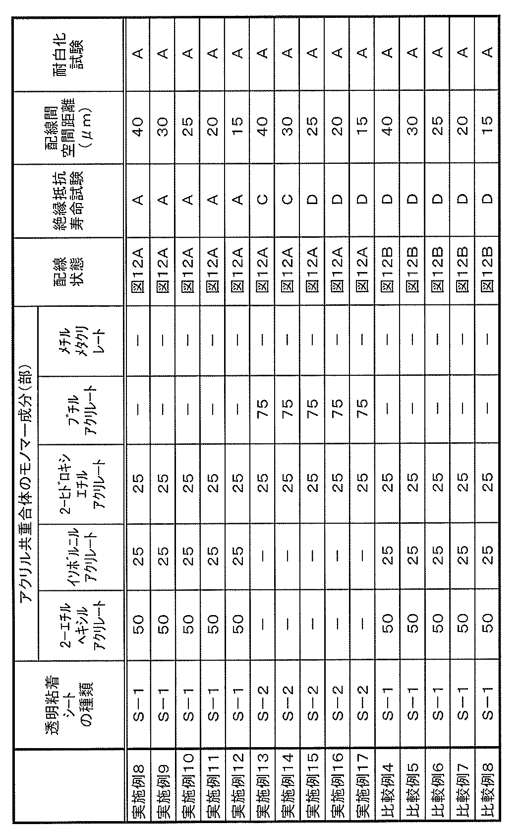
表4から、図12Bに示す配線状態で評価した比較例4~8は、いずれもマイグレーション評価が「D」であった。これに対して、透明両面粘着シートS-1を使用し、且つ、図12Aに示す配線状態で評価した実施例8~12は、配線間の空間距離の変化にも拘わらず、評価が「A」であり、非常に良好であった。透明両面粘着シートS-2を使用し、且つ、図12Aに示す配線状態で評価した実施例13~17は、配線間の空間距離が狭くなるに従ってマイグレーション評価が劣化する傾向にあった。
なお、本発明に係る配線基板は、上述の実施の形態に限らず、本発明の要旨を逸脱することなく、種々の構成を採り得ることはもちろんである。
Claims (11)
- 絶縁基板(32A)上に配置された複数の金属配線と、前記金属配線と直接接触して前記金属配線上に配置された透明粘着剤層(34A)とを有する配線基板であって、
前記金属配線は、
第1パルス信号(P1)が供給される第1金属配線(50a)と、
前記第1金属配線(50a)に前記第1パルス信号(P1)が供給されている期間に前記第1パルス信号(P1)に同期した第2パルス信号(P2)が供給され、それ以外の期間に固定電位が印加される第2金属配線(54a)とを有することを特徴とする配線基板。 - 請求項1記載の配線基板において、
前記金属配線は銀及び/又は銅を含むことを特徴とする配線基板。 - 請求項1記載の配線基板において、
前記第1パルス信号(P1)及び前記第2パルス信号(P2)の各基準レベルは、前記固定電位と同じレベルであり、
前記第1パルス信号(P1)の振幅の絶対値(|A1|)と前記第2パルス信号(P2)の振幅の絶対値(|A2|)との差が前記第1パルス信号(P1)の振幅の絶対値(|A1|)の1/2以下であることを特徴とする配線基板。 - 請求項1記載の配線基板において、
前記第1パルス信号(P1)と前記第2パルス信号(P2)とが同じパルス信号であることを特徴とする配線基板。 - 請求項1記載の配線基板において、
前記透明粘着剤層(34A)は、光学的に透明な下記構成成分A、構成成分B及び構成成分Cとからなる群から選択される少なくとも1つから構成された透明粘着剤を有し、
前記透明粘着剤を100部としたとき、前記構成成分Aは45~95部含み、前記構成成分Bは20~50部含み、前記構成成分Cは1~40部含むことを特徴とする配線基板。
構成成分A:25℃以下のガラス転移温度Tgを有するアルキル(メタ)アクリレートモノマー(ここで、アルキル基が4~18個の炭素原子を有する)。
構成成分B:25℃以上のガラス転移温度Tgを有する(メタ)アクリレートモノマーのエステル。
構成成分C:ヒドロキシアルキル(メタ)アクリレート、非置換(メタ)アクリルアミド、N-アルキル置換(メタ)アクリルアミド、N,N-ジアルキル置換(メタ)アクリルアミド、尿素官能基を有するモノマー、ラクタム官能基、三級アミン、脂環式アミン、芳香族アミン、及びこれらの組み合わせを有するモノマーからなる群から選択されるモノマー。 - 請求項5記載の配線基板において、
前記構成成分Aは、n-ブチルアクリレート、2-エチル-ヘキシル(メタ)アクリレート、イソオクチルアクリレート、2-メチルヘキシルアクリレート、及びこれらの組み合わせからなる群から選択される少なくとも1つであることを特徴とする配線基板。 - 請求項5記載の配線基板において、
前記構成成分Bは、メチル(メタ)アクリレート、エチル(メタ)アクリレート、イソボルニル(メタ)アクリレート、及びこれらの組み合わせからなる群から選択される少なくとも1つであることを特徴とする配線基板。 - 請求項5記載の配線基板において、
前記構成成分Cは、2-ヒドロキシエチル(メタ)アクリレート、3-ヒドロキシプロピル(メタ)アクリレート、N-オクチルアクリルアミド、N,N-ジメチルアクリルアミド、N,N-ジエチルアクリルアミド、ビニルピリジン、ビニルイミダゾール、N,N-ジアルキルアミノアルキル(メタ)アクリレート(ここで、アルキル基は、1~4個の炭素原子を有する)、及びこれらの組み合わせからなる群から選択される少なくとも1つであることを特徴とする配線基板。 - 請求項5記載の配線基板において、
前記構成成分Aが2-エチル-ヘキシル(メタ)アクリレート、前記構成成分Bがイソボルニル(メタ)アクリレート、前記構成成分Cが2-ヒドロキシエチル(メタ)アクリレートであることを特徴とする配線基板。 - 請求項5記載の配線基板において、
前記透明粘着剤は、
前記構成成分Aとして、2-エチル-ヘキシル(メタ)アクリレートを50~65部含み、前記構成成分Bとして、イソボルニル(メタ)アクリレートを15~30部含み、前記構成成分Cとして、2-ヒドロキシエチル(メタ)アクリレートを20~30部含むことを特徴とする配線基板。 - 請求項5記載の配線基板において、
前記構成成分Aがn-ブチルアクリレート、前記構成成分Cが2-ヒドロキシエチル(メタ)アクリレートであることを特徴とする配線基板。
Applications Claiming Priority (2)
| Application Number | Priority Date | Filing Date | Title |
|---|---|---|---|
| JP2013-071869 | 2013-03-29 | ||
| JP2013071869A JP5864469B2 (ja) | 2013-03-29 | 2013-03-29 | 配線基板 |
Publications (1)
| Publication Number | Publication Date |
|---|---|
| WO2014157281A1 true WO2014157281A1 (ja) | 2014-10-02 |
Family
ID=51624246
Family Applications (1)
| Application Number | Title | Priority Date | Filing Date |
|---|---|---|---|
| PCT/JP2014/058426 Ceased WO2014157281A1 (ja) | 2013-03-29 | 2014-03-26 | 配線基板 |
Country Status (3)
| Country | Link |
|---|---|
| JP (1) | JP5864469B2 (ja) |
| TW (1) | TW201503772A (ja) |
| WO (1) | WO2014157281A1 (ja) |
Citations (4)
| Publication number | Priority date | Publication date | Assignee | Title |
|---|---|---|---|---|
| JP2006039927A (ja) * | 2004-07-27 | 2006-02-09 | Fujitsu Component Ltd | タッチパネルの制御装置および制御方法 |
| JP2011501767A (ja) * | 2007-09-28 | 2011-01-13 | スリーエム イノベイティブ プロパティズ カンパニー | インジウムスズ酸化物に適合した光学的に透明な接着剤 |
| JP2011221949A (ja) * | 2010-04-14 | 2011-11-04 | Panasonic Corp | タッチパネル装置 |
| JP2013105327A (ja) * | 2011-11-14 | 2013-05-30 | Japan Display East Co Ltd | タッチパネル |
-
2013
- 2013-03-29 JP JP2013071869A patent/JP5864469B2/ja active Active
-
2014
- 2014-03-26 WO PCT/JP2014/058426 patent/WO2014157281A1/ja not_active Ceased
- 2014-03-27 TW TW103111361A patent/TW201503772A/zh unknown
Patent Citations (4)
| Publication number | Priority date | Publication date | Assignee | Title |
|---|---|---|---|---|
| JP2006039927A (ja) * | 2004-07-27 | 2006-02-09 | Fujitsu Component Ltd | タッチパネルの制御装置および制御方法 |
| JP2011501767A (ja) * | 2007-09-28 | 2011-01-13 | スリーエム イノベイティブ プロパティズ カンパニー | インジウムスズ酸化物に適合した光学的に透明な接着剤 |
| JP2011221949A (ja) * | 2010-04-14 | 2011-11-04 | Panasonic Corp | タッチパネル装置 |
| JP2013105327A (ja) * | 2011-11-14 | 2013-05-30 | Japan Display East Co Ltd | タッチパネル |
Also Published As
| Publication number | Publication date |
|---|---|
| JP2014197584A (ja) | 2014-10-16 |
| JP5864469B2 (ja) | 2016-02-17 |
| TW201503772A (zh) | 2015-01-16 |
Similar Documents
| Publication | Publication Date | Title |
|---|---|---|
| JP5864470B2 (ja) | 配線基板 | |
| WO2015005319A1 (ja) | 配線基板 | |
| JP6092363B2 (ja) | 粘着フィルム、タッチパネル用積層体 | |
| CN106132687B (zh) | 导电膜层叠体以及使用该导电膜层叠体的触摸面板 | |
| US10125294B2 (en) | Adhesive sheet, laminate for touch panel, and capacitance-type touch panel | |
| US20160216809A1 (en) | Laminate for touch panel | |
| JP6267340B2 (ja) | 静電容量式タッチパネル | |
| WO2016140131A1 (ja) | タッチパネル用粘着シート、タッチパネル用積層体、静電容量式タッチパネル | |
| WO2015025803A1 (ja) | タッチパネル用粘着シート、タッチパネル用積層体、静電容量式タッチパネル | |
| EP3037930A1 (en) | Capacitive touch panel | |
| JP5864469B2 (ja) | 配線基板 | |
| JP2015166900A (ja) | タッチパネル用粘着フィルムおよびタッチパネル用積層体 | |
| WO2015107759A1 (ja) | 導電性フイルム |
Legal Events
| Date | Code | Title | Description |
|---|---|---|---|
| 121 | Ep: the epo has been informed by wipo that ep was designated in this application |
Ref document number: 14774447 Country of ref document: EP Kind code of ref document: A1 |
|
| NENP | Non-entry into the national phase |
Ref country code: DE |
|
| 122 | Ep: pct application non-entry in european phase |
Ref document number: 14774447 Country of ref document: EP Kind code of ref document: A1 |