WO2014148457A1 - セラミックパッケージ及び電子部品 - Google Patents
セラミックパッケージ及び電子部品 Download PDFInfo
- Publication number
- WO2014148457A1 WO2014148457A1 PCT/JP2014/057225 JP2014057225W WO2014148457A1 WO 2014148457 A1 WO2014148457 A1 WO 2014148457A1 JP 2014057225 W JP2014057225 W JP 2014057225W WO 2014148457 A1 WO2014148457 A1 WO 2014148457A1
- Authority
- WO
- WIPO (PCT)
- Prior art keywords
- mass
- layer
- ceramic package
- ceramic
- powder
- Prior art date
- Legal status (The legal status is an assumption and is not a legal conclusion. Google has not performed a legal analysis and makes no representation as to the accuracy of the status listed.)
- Ceased
Links
Images
Classifications
-
- H—ELECTRICITY
- H10—SEMICONDUCTOR DEVICES; ELECTRIC SOLID-STATE DEVICES NOT OTHERWISE PROVIDED FOR
- H10W—GENERIC PACKAGES, INTERCONNECTIONS, CONNECTORS OR OTHER CONSTRUCTIONAL DETAILS OF DEVICES COVERED BY CLASS H10
- H10W76/00—Containers; Fillings or auxiliary members therefor; Seals
- H10W76/60—Seals
-
- H—ELECTRICITY
- H10—SEMICONDUCTOR DEVICES; ELECTRIC SOLID-STATE DEVICES NOT OTHERWISE PROVIDED FOR
- H10W—GENERIC PACKAGES, INTERCONNECTIONS, CONNECTORS OR OTHER CONSTRUCTIONAL DETAILS OF DEVICES COVERED BY CLASS H10
- H10W76/00—Containers; Fillings or auxiliary members therefor; Seals
- H10W76/10—Containers or parts thereof
- H10W76/12—Containers or parts thereof characterised by their shape
- H10W76/15—Containers comprising an insulating or insulated base
-
- H—ELECTRICITY
- H10—SEMICONDUCTOR DEVICES; ELECTRIC SOLID-STATE DEVICES NOT OTHERWISE PROVIDED FOR
- H10W—GENERIC PACKAGES, INTERCONNECTIONS, CONNECTORS OR OTHER CONSTRUCTIONAL DETAILS OF DEVICES COVERED BY CLASS H10
- H10W76/00—Containers; Fillings or auxiliary members therefor; Seals
- H10W76/10—Containers or parts thereof
- H10W76/17—Containers or parts thereof characterised by their materials
Definitions
- the present invention relates to a ceramic package, for example, a ceramic package and an electronic component suitable for mounting an element such as a vibrator inside.
- Ceramic packages for mounting elements such as vibrators are known.
- This ceramic package is configured by sealing a metal lid member, for example, by seam welding, using a high-temperature sealing material such as silver brazing in a ceramic container having an upper surface opening.
- a metallized layer and a nickel (Ni) plating layer are interposed between a container and a high temperature sealing material, and the thickness of the metallized layer and the Ni plating layer is adjusted.
- the occurrence of cracks is suppressed.
- the thickness of the metallizing layer for sealing is made thicker than that of the Ni plating layer, the electric resistance of the metallizing layer for sealing becomes low, and it becomes difficult for the welding current to flow to the metal lid during seam welding. Therefore, an extremely large welding current must be applied, and the thermal stress due to the large welding current also increases, so that the residual stress between the insulating substrate and the lid after welding causes cracks in the metallization layer for sealing and the insulating substrate. Has a problem that it is likely to occur.
- an electroless Ni plating layer is used for a sealing portion of a ceramic package for sealing a metal lid using a high-temperature sealing material such as silver solder, the Ni plating layer and the ceramic portion are sealed after sealing.
- a high-temperature sealing material such as silver solder
- an electrolytic Ni plating layer has been used.
- An object of the present invention is to provide a ceramic package and an electronic component that can be formed without causing any cracks, can suppress the generation of cracks when sealed with a high-temperature sealing material, and have high hermetic reliability.
- a ceramic container having an upper surface opening having a bottom and a side wall and a lid for closing the opening of the container are sealed using a high-temperature sealing material.
- the container has a bonding layer between an upper end surface of the side wall and the high-temperature sealing material in the container, and the bonding layer includes a metallization layer formed on the upper end surface of the side wall, and the metallization layer.
- the stress relaxation layer is an electroless plating layer having a film hardness (Vickers hardness) of 50 or more and less than 500.
- the stress relaxation layer may be an electroless plating layer containing nickel (Ni) as a main component.
- the stress relaxation layer is preferably an electroless plating layer in which boron (B) is contained in the nickel (Ni) in an amount of 0.01% by mass or more and less than 1.0% by mass.
- the stress relaxation layer is more preferably an electroless plating layer in which boron (B) is contained in an amount of 0.01% by mass to 0.3% by mass in the nickel (Ni).
- the stress relaxation layer is preferably an electroless plating layer in which phosphorus (P) is contained in the nickel (Ni) in an amount of 0.01% by mass to less than 8% by mass.
- the stress relaxation layer is more preferably an electroless plating layer in which phosphorus (P) is contained in an amount of 0.01% by mass to 1.5% by mass in the nickel (Ni).
- the container may be formed of a ceramic substrate having a bending strength of 500 MPa or more.
- the ceramic substrate includes Al 2 O 3 as a main crystal phase, and further includes a MnTiO 3 crystal phase and a MnAl 2 O 4 crystal phase, and has a specific gravity greater than 3.6.
- the bonding layer may further include an electroless plating layer of at least a noble metal between the stress relaxation layer and the high temperature sealing material.
- the stress relaxation layer may function as a layer for improving the wettability of the brazing material together with the electroless plating layer of the noble metal.
- An electronic component according to a second aspect of the present invention includes the element sealed in the container of the ceramic package according to the first aspect of the present invention described above.
- an electrically independent wiring pattern can be formed without increasing man-hours by forming an electroless plating layer having a film hardness of 50 or more and less than 500 as a stress relaxation layer. Moreover, when sealed with a high-temperature sealing material, the generation of cracks can be suppressed, and a ceramic package with high hermetic reliability can be obtained. This leads to an improvement in the reliability of the ceramic package, a reduction in cost, an improvement in yield, and an improvement in productivity.
- ⁇ indicating a numerical range is used as a meaning including numerical values described before and after the numerical value as a lower limit value and an upper limit value.
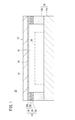
- a ceramic package 10 includes a ceramic container 12 having an upper surface opening having a bottom portion 12a and a side wall 12b, and a metal lid body 14 that closes the opening of the container 12. And are hermetically sealed using a high-temperature sealing material 16 such as silver solder.
- At least one element 20 of, for example, a crystal resonator, a resistor, a filter, a capacitor, and a semiconductor element. Is mounted and sealed, whereby the electronic component 22 according to the present embodiment is configured.
- the joining layer 24 is interposed between the upper end surface of the side wall 12b of the container 12, and the high temperature sealing material 16.
- the bonding layer 24 has a metallized layer 26 formed on the upper end surface of the side wall 12 b and a stress relaxation layer 28 formed on the metalized layer 26. And this stress relaxation layer 28 is comprised by the electroless-plating layer whose film hardness (Vickers hardness) is 50-500.
- the container 12 is made of a ceramic substrate. Ceramic green body, the Al 2 O 3 as the main crystal phase, other, MnTiO 3 crystal phase alone, or including MnTiO 3 crystal phase and MnAl 2 O 4 crystalline phase.
- Al is 85.0 to 95.0% by mass in terms of Al 2 O 3
- Mg is 0.1 to 0.6% by mass in terms of MgO
- Si is 2.0 to 6 in terms of SiO 2 .
- Mn 2.4-7.1% by mass in terms of MnCO 3 and Ti 0.1-2.0% by mass in terms of TiO 2 .
- the content ratio of SiO 2 and MgCO 3 is preferably larger than 1 in terms of SiO 2 / MgO.
- the ceramic substrate is composed of 85.0 to 95.0 mass% of Al 2 O 3 powder, 0.1 to 0.6 mass% of MgO powder, and 2.0 to 6.0 mass of SiO 2 powder. %, MnCO 3 powder 2.4-7.1% by mass and TiO 2 powder 0.1-2.0% by mass, and then the molded body is fired at 1200-1400 ° C. It is produced by this.
- MgO powder is added as a sintering aid for Al 2 O 3
- SiO 2 powder is added as a sintering aid for Al 2 O 3 in order to lower the sintering temperature.
- the MnCO 3 powder is added to produce a Mn 2 SiO 4 glass phase to lower the sintering temperature and to produce MnTiO 3 crystals to improve the strength of the glass phase.
- the TiO 2 powder is added to produce MnTiO 3 crystals and improve the strength of the glass phase.
- sintering can be performed at a low temperature of 1200 to 1400 ° C., and a ceramic body having a bending strength of 500 MPa or more can be realized. If the bending strength is lower than 500 MPa, thermal stress may be applied during the sealing of the lid body 14 or the secondary mounting, resulting in destruction. Alternatively, there is a risk of destruction due to an impact or the like during handling or use. If the bending strength is 500 MPa or more, such a risk of destruction can be avoided.
- the “bending strength” refers to a four-point bending strength, which is a value measured at room temperature based on JIS R1601 (bending test method for fine ceramics).
- the lid body 14 is formed in a flat plate shape having a thickness of 0.05 to 0.20 mm, and is made of an iron-nickel alloy plate or an iron-nickel-cobalt alloy plate.
- a brazing material such as a silver-copper eutectic brazing which is a high-temperature sealing material 16 is formed on the lower surface (the entire surface or a portion corresponding to the side wall 12 b) of the lid body 14. The thickness is about 5 to 20 ⁇ m.
- the lid body 14 is formed by punching a composite plate formed by rolling an iron-nickel alloy plate or an iron-nickel-cobalt alloy plate with a brazing filler metal foil such as silver-copper brazing. Is manufactured by punching into a predetermined shape.
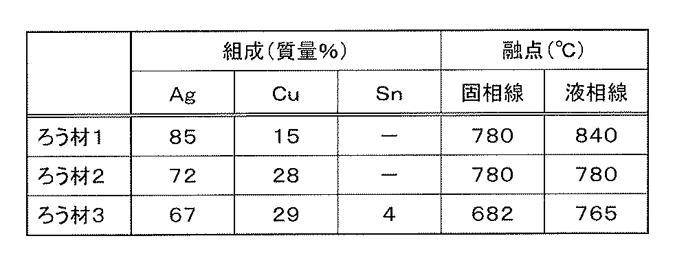
- any one of the brazing material 1 (85Ag-15Cu), the brazing material 2 (72Ag-28Cu) and the brazing material 3 (67Ag-29Cu-4Sn) shown in Table 1 below is used. Can be used.
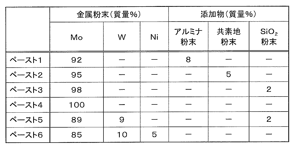
- the metallized layer 26 is formed of a conductor paste containing at least one of metal powders such as W (tungsten), Mo (molybdenum), and nickel (Ni) as a conductor component (main component).
- metal powders such as W (tungsten), Mo (molybdenum), and nickel (Ni) as a conductor component (main component).
- the electroless plating layer that is the stress relaxation layer 28 is preferably an electroless plating layer mainly composed of Ni. Specifically, it is an electroless plating layer containing Ni as a main component and containing boron (B) or phosphorus (P) as an additive.
- Ni is contained in B
- it is preferably an electroless plating layer in which B is contained in Ni in an amount of 0.01% by mass or more and less than 1.0% by mass, and more preferably, B is 0.01% in Ni.
- the electroless plating layer is contained in an amount of 0.3% to 0.3% by mass.
- Ni contains P
- it is preferably an electroless plating layer in which P is contained in Ni in an amount of 0.01% by mass or more and less than 8.0% by mass, and more preferably, Ni contains P in an amount of 0.01% by mass.
- % Is an electroless plating layer containing 1.5% by mass or more and 1.5% by mass or less.
- the reason why the lower limit of the addition amount of B or P is set to 0.01% by mass is to maintain the reactivity of the Ni plating layer in electroless plating.
- dimethylamine borane and sodium hypophosphite containing B and P as reducing agents in electroless plating, if the reducing agent is reduced in the plating reaction tank, the reduction effect is not sufficient and the reactivity cannot be maintained. This is because cases are likely to occur.
- the reducing agent it is also possible to use hydrazine or the like that does not contain B or P metal ions. Also in this case, in order to maintain the reaction stability at the time of plating, dimethylamine borane, sodium hypophosphite and the like are used, and as a result, the addition amounts of B and P are 0.01% by mass or more.
- the bonding layer 24 includes a noble metal electroless plating layer 30 in addition to the stress relaxation layer 28 described above.
- the noble metal electroless plating layer 30 is formed between the high temperature sealing material 16 and the stress relaxation layer 28, and an electroless plating layer 30a of, for example, palladium (Pb) formed on the stress relaxation layer 28, for example, an electroless plating layer 30b made of gold (Au) is formed on the electroless plating layer 30a.
- the noble metal electroless plating layer 30 is formed for the purpose of improving the wettability of the high temperature sealing material 16, and the lower stress relaxation layer 28 is also used together with the noble metal electroless plating layer 30. It functions as a layer that improves the wettability of the metallized layer 26.
- an electrically independent wiring pattern can be increased in man-hours.
- the high-temperature sealing material 16 is used for sealing, the generation of cracks can be suppressed, and the ceramic package 10 with high hermetic reliability can be obtained. This leads to an improvement in the reliability of the ceramic package 10, a reduction in cost, an improvement in yield, and an improvement in productivity.
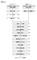
- step S1 of FIG. 2 raw material powder, an organic component and a solvent for preparing a ceramic tape are prepared.
- the raw material powders to be prepared are Al 2 O 3 powder 85.0 to 95.0 mass%, MgO powder 0.1 to 0.6 mass%, SiO 2 powder 2.0 to 6.0 mass%, MnCO 3 Mixed powder containing 2.4 to 7.1% by mass of powder and 0.1 to 2.0% by mass of TiO 2 powder.
- the average particle size of these powders is, for example, 0.7 to 2.5 ⁇ m for Al 2 O 3 powder, 0.1 to 1.0 ⁇ m for MgO powder, 0.1 to 2.5 ⁇ m for SiO 2 powder, and MnCO 3 powder. 0.5 to 4.0 ⁇ m, and TiO 2 powder 0.1 to 0.5 ⁇ m.
- the powder particle size is measured by, for example, a laser diffraction / scattering method.
- Examples of the organic component (binder) to be prepared include a resin, a surfactant, and a plasticizer.
- the resin include polyvinyl butyral
- examples of the surfactant include tertiary amines
- examples of the plasticizer include phthalic acid esters (for example, diisononyl phthalate: DINP).
- Examples of the solvent to be prepared include alcohol solvents and aromatic solvents.
- Examples of the alcohol solvent include IPA (isopropyl alcohol), and examples of the aromatic solvent include toluene.
- step S2 the organic powder and the solvent are mixed and dispersed in the above-mentioned mixed powder.
- step S3 the ceramic substrate is formed by a known forming method such as a pressing method, a doctor blade method, a rolling method, or an injection method.
- a ceramic molded body (ceramic tape) which is a precursor of the above is prepared.
- an organic component and a solvent are added to the mixed powder to prepare a slurry, and then a ceramic tape having a predetermined thickness is produced by a doctor blade method.
- an organic component is added to the mixed powder, and a ceramic tape having a predetermined thickness is produced by press molding, rolling molding, or the like.
- step S4 the ceramic tape is cut and processed into a desired shape to produce, for example, a first tape for the bottom of the container and a second tape for the side wall of the container. If necessary, through holes for via holes are formed by micro drilling, laser processing, or the like.
- a raw material powder, an organic component and a solvent for the conductor paste are prepared.
- the raw material powder to be prepared is equivalent to at least one of metal powders such as W (tungsten), Mo (molybdenum), nickel (Ni) and the like, and Al 2 O 3 powder, SiO 2 powder, or ceramic substrate as appropriate.
- a mixed powder obtained by adding 1 to 20% by mass, particularly 8% by mass or less of the above powder.
- Examples of the organic component to be prepared include a resin (for example, ethyl cellulose) and a surfactant.
- Examples of the solvent to be prepared include terpenol.
- step S6 a conductive paste is prepared by mixing and dispersing the organic component and the solvent in the mixed powder.
- step S7 a conductor paste is printed and applied to the first tape and the second tape produced as described above by a method such as screen printing or gravure printing.
- step S8 the first tape and the second tape on which the conductor paste is printed and applied are aligned and laminated and pressure-bonded to produce a laminate.
- a forming gas atmosphere wetter temperature 25 to 47 ° C.
- a laminated original sheet in which the laminate and the conductor paste are simultaneously fired is produced.
- This laminated original plate has a shape in which the shapes of many containers 12 are integrally arranged.
- the conductor paste becomes the metallized layer 26 by this firing.
- the oxidation of the metal in the conductor paste can be prevented by performing the firing atmosphere in the forming gas atmosphere as described above.
- the firing temperature is preferably in the temperature range described above. When the firing temperature is lower than 1200 ° C., the densification is insufficient and the bending strength does not reach 500 MPa. When the firing temperature is higher than 1400 ° C., the shrinkage of the first tape and the second tape constituting the laminate varies. Increases and the dimensional accuracy decreases. This leads to a decrease in yield and increases the cost. Of course, the higher the firing temperature, the more expensive the equipment.
- the surface of the metallized layer 26 is washed with alkali, acid or the like (pretreatment).
- step S11 Ni electroless plating is performed to form a Ni electroless plating layer on the metallized layer 26, that is, a stress relaxation layer 28 (film thickness: 1.0 to 5.0 ⁇ m). If necessary, heat treatment is performed in an atmosphere containing H 2 gas.
- step S12 Pd electroless plating treatment is performed to form a Pd electroless plating layer 30a (film thickness: 0.1 to 0.8 ⁇ m) on the stress relaxation layer 28.
- step S13 Au Then, an electroless plating layer 30b (thickness: 0.05 to 0.5 ⁇ m) of Au is formed on the electroless plating layer 30a of Pd.
- step S14 each element 20 is mounted in the accommodation space 18 of each container 12 formed integrally with the laminated original plate.
- step S15 the characteristics of each element 20 are inspected in the state of the laminated original sheet, and then in step S16, the laminated original sheet is divided into a plurality of containers 12 each having the element 20 mounted in the accommodation space 18.
- step S ⁇ b> 17 the lid body 14 having the high temperature sealing material 16 formed on the back surface is placed on the container 12 with the high temperature sealing material 16 facing the side wall 12 b (bonding layer 24) of the container 12. . Thereafter, while rolling a pair of roller electrodes of the seam welding machine in contact with the opposing outer peripheral edges of the lid 14, a part of the high-temperature sealing material 16 is melted by passing an electric current between the roller electrodes. By doing so, the lid 14 is hermetically sealed on the side wall 12 b of the container 12. The atmosphere at the time of sealing is performed in N 2 gas or vacuum.
- the metallized layer 26 and the stress relaxation layer 28 are interposed between the ceramic package 10 in which the element 20 is accommodated in the container 12, that is, the upper end surface of the side wall 12 b of the container 12 and the high-temperature sealing material 16.
- the ceramic package 10 in which the relaxing layer 28 is configured with an electroless plating layer having at least a film hardness (Vickers hardness) of 50 or more and less than 500 is completed.
- the raw material powder includes an Al 2 O 3 powder having an average particle size of 1.5 ⁇ m, an MgO powder having an average particle size of 0.5 ⁇ m, an SiO 2 powder having an average particle size of 4.0 ⁇ m, an MnCO 3 powder having an average particle size of 3.0 ⁇ m, and an average TiO 2 powder having a particle size of 0.25 ⁇ m.
- a ceramic tape having a thickness of 60 to 270 ⁇ m was produced by a doctor blade method. The obtained ceramic tape was fired at 1330 ° C. to prepare a substrate 1.
- Base 3 A substrate 3 was prepared in the same manner as the substrate 1 described above except that the average particle diameter of the MnCO 3 powder was 1.0 ⁇ m among the raw material powders.
- a substrate 5 was prepared in the same manner as the substrate 1 described above, except that among the raw material powders, the Al 2 O 3 powder was 90.2 mass% and the MgO powder was 0.10 mass%.
- a substrate 6 was produced in the same manner as the substrate 1 described above except that the raw material powder was 90.9 mass% Al 2 O 3 powder and 0.1 mass% TiO 2 powder.
- Base 7 Among the raw material powders, Al 2 O 3 powder is 87.6 mass%, SiO 2 powder is 5.0 mass%, MnCO 3 powder is 5.9 mass%, TiO 2 powder is 1.2 mass%, SiO 2 A substrate 7 was produced in the same manner as the substrate 1 described above except that / MnCO 3 was 1.37 in terms of SiO 2 / MnO and the firing temperature was 1280 ° C.
- a substrate 9 was produced in the same manner as the substrate 1 described above, except that among the raw material powders, Al 2 O 3 powder was 89.3 mass% and TiO 2 powder was 2.0 mass%.
- the substrate 10 is produced in the same manner as the substrate 1 described above except that the Al 2 O 3 powder is 89.7 mass%, the MgO powder is 0.60 mass%, and the firing temperature is 1310 ° C. did.
- Al 2 O 3 powder is 92.0% by mass
- MgO powder is 0.34% by mass
- SiO 2 powder is 3.4% by mass
- MnCO 3 powder is 6.4% by mass
- TiO 2 powder is A substrate 12 was produced in the same manner as the substrate 1 described above except that the content was 0.0% by mass and SiO 2 / MnCO 3 was 0.87 in terms of SiO 2 / MnO.
- Al 2 O 3 powder is 90.2 mass%
- MgO powder is 0.34 mass%
- SiO 2 powder is 4.4 mass%
- MnCO 3 powder is 5.0 mass%
- TiO 2 powder is A substrate 13 was produced in the same manner as the substrate 1 described above except that the content was 0.0% by mass and SiO 2 / MnCO 3 was 1.43 in terms of SiO 2 / MnO.
- Base 15 Of the raw material powder, Al 2 O 3 powder is 88.4 mass%, SiO 2 powder is 2.9 mass%, MnCO 3 powder is 8.5 mass%, and SiO 2 / MnCO 3 is converted to SiO 2 / MnO.
- a substrate 15 was produced in the same manner as the substrate 1 described above except for 0.55.
- a substrate 16 was produced in the same manner as the substrate 1 described above, except that 0.02 mass% of the TiO 2 powder was used as the raw material powder.
- a substrate 17 was prepared in the same manner as the substrate 1 described above, except that among the raw material powders, Al 2 O 3 powder was 91.3 mass% and MgO powder was 0.00 mass%.
- the substrates 1 to 17 were measured by the Archimedes method using the medium as water.
- the substrates 1 to 17 were measured at room temperature based on the four-point bending strength test of JIS R1601.
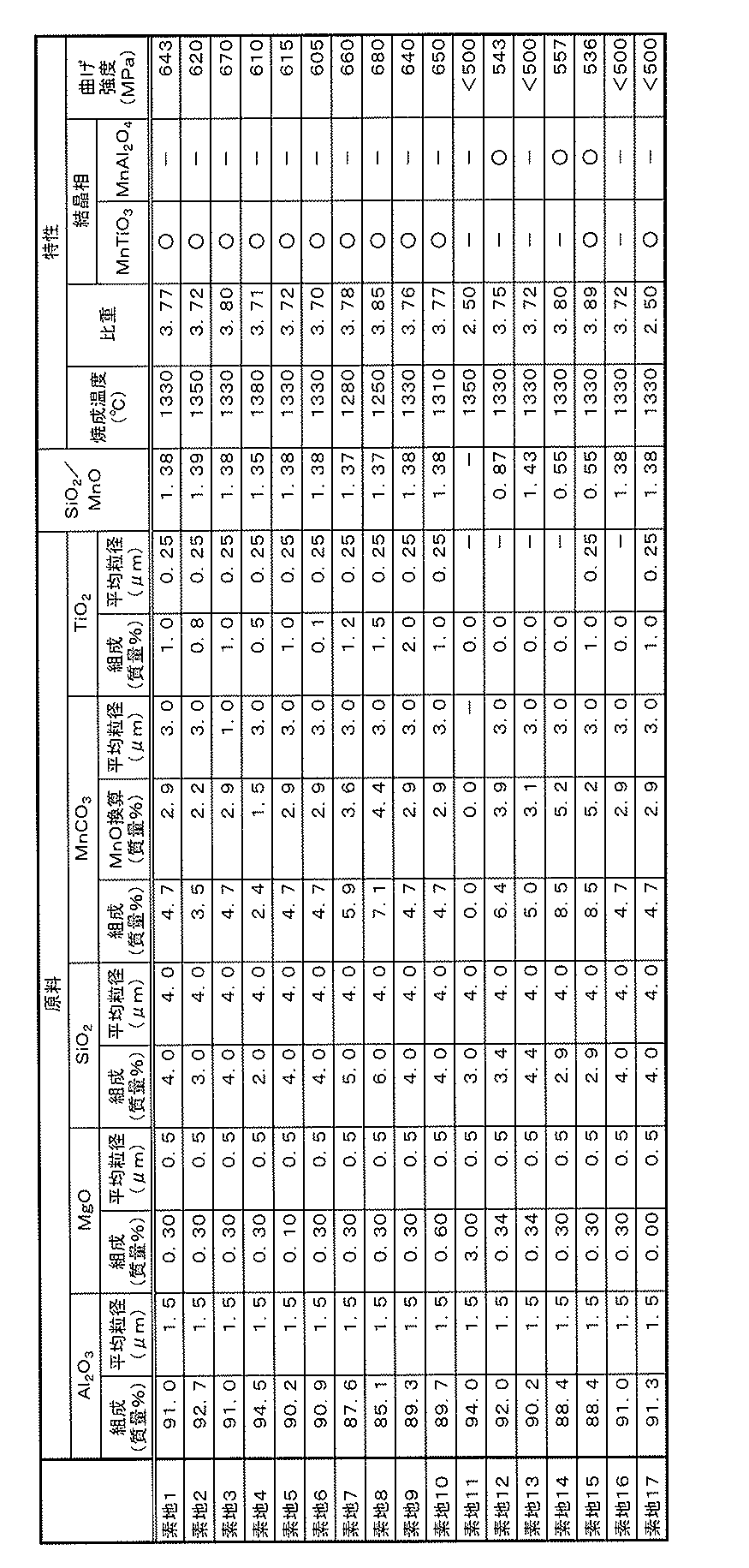
- the breakdown and characteristics (specific gravity, crystal phase, bending strength) of the above-mentioned substrates 1 to 17 are shown in Table 2 below.
- Example 1 The substrate 1 is used as the ceramic substrate, the paste 1 is used as the conductor paste, the composition of the stress relaxation layer 28 is Ni—B (B is 0.9 mass%), and 625 in accordance with the manufacturing method shown in FIG. Individual samples 1 were prepared. As the high-temperature sealing material 16, the brazing material 3 in Table 1 described above was used. The thickness of the stress relaxation layer 28 was 3 ⁇ m. Similarly, 625 samples 2 to 6 were produced using pastes 2 to 6 as conductor pastes, respectively. This was designated Example 1.
- Examples 2 to 6 In the same manner as in Example 1, the amount of addition of B in the composition Ni—B of the stress relaxation layer 28 was changed, and Example 2 (Samples 7 to 12), Example 3 (Samples 13 to 18), and Example 4 ( Samples 19 to 24), Example 5 (Samples 25 to 30), and Example 6 (Samples 31 to 36) were produced.
- the addition amount of B was 0.5 mass% in Example 2, 0.3 mass% in Example 3, 0.1 mass% in Example 4, and 0.05 mass% in Example 5.
- Example 6 is 0.01 mass%.
- Example 7 Samples 37 to 42 were produced in the same manner as in Example 1 except that the composition of the stress relaxation layer 28 was Ni—P (P was 7.0 mass%).
- Example 8 In the same manner as in Example 7, the amount of addition of P in the composition Ni—P of the stress relaxation layer 28 was changed, and Example 8 (Samples 43 to 48), Example 9 (Samples 49 to 54), and Example 10 ( Samples 55 to 60), Example 11 (Samples 61 to 66), and Example 12 (Samples 67 to 72) were produced.
- the amount of P added was 5.0 mass% in Example 8, 3.0 mass% in Example 9, 1.5 mass% in Example 10, 1.0 mass% in Example 11, and Example 12 is 0.01 mass%.
- Example 2 Samples 79 to 84 were produced in the same manner as in Example 1 except that the composition of the stress relaxation layer 28 was Ni—B (B was 1.0 mass%).
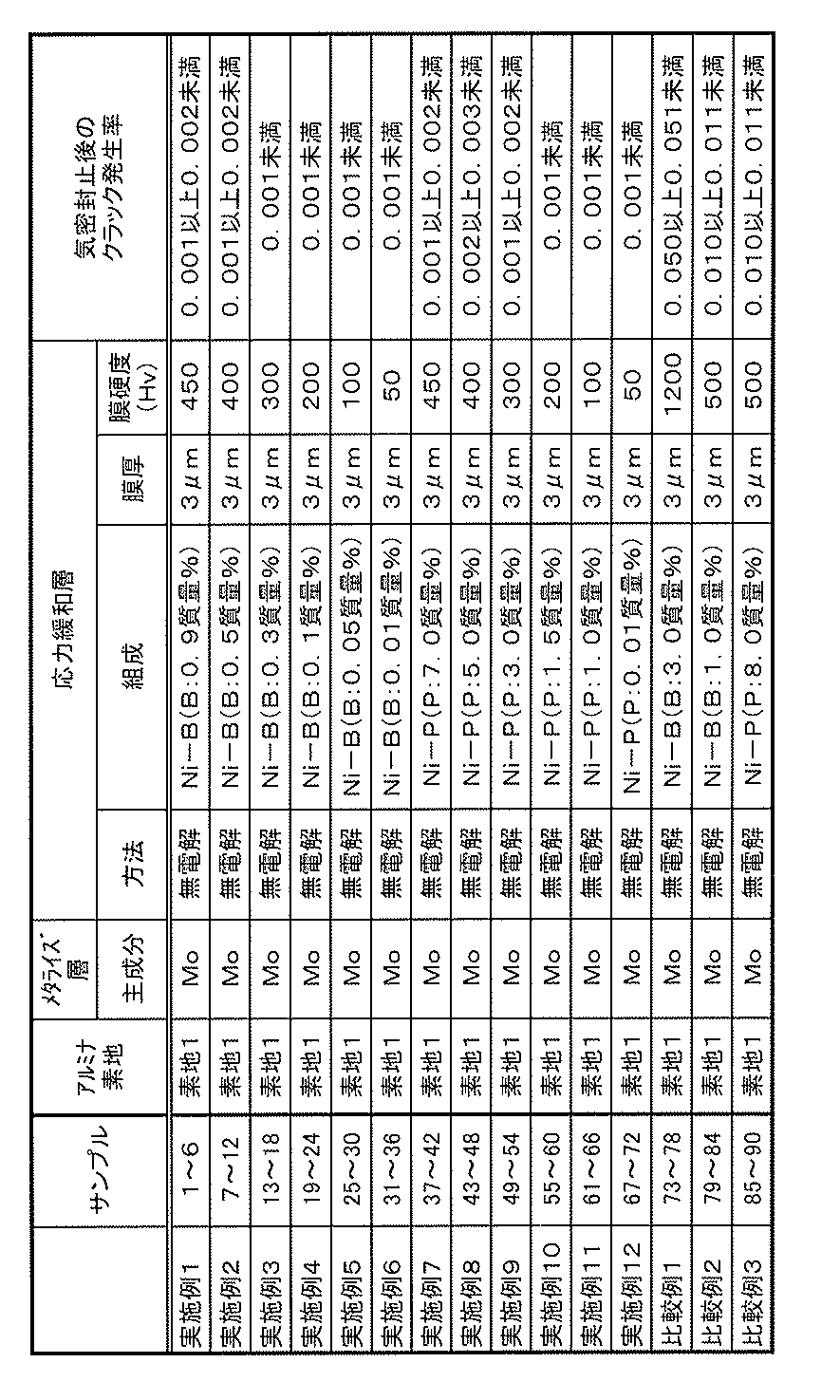
- Examples 1 to 12 having a film hardness of less than 500 were all good with a crack generation rate of less than 0.002 after hermetic sealing.
- the crack occurrence rate was less than 0.001, which was very good.
- the film hardness of the stress relaxation layer 28 composed of the electroless plating layer is preferably 50 or more and less than 500, and more preferably 50 or more and 300 or less.
- Example 21 The substrate 1 is used as the ceramic substrate, the paste 1 is used as the conductor paste, the composition of the stress relaxation layer 28 is Ni—B (B is 0.3 mass%), and 625 in accordance with the manufacturing method shown in FIG. Samples 101 were produced. The thickness of the stress relaxation layer 28 was 3 ⁇ m. Similarly, 625 samples 102 to 106 were prepared using pastes 2 to 6 as conductor pastes, respectively. This was designated as Example 21. This Example 21 is the same as Example 3 in the first example.
- Example 22 to 37 Example 22 to 37 were produced in the same manner as in Example 21 except that the ceramic substrate to be used was changed. Here, the ceramic substrates used were the substrates 2 to 17 in Examples 22 to 37.
- the ceramic substrates having a bending strength of 500 MPa or more are the substrates 1 to 10, 12, 14, and 15, and the ceramic substrates having a bending strength of less than 500 MPa are the substrates 11, 13, 16 and 17.
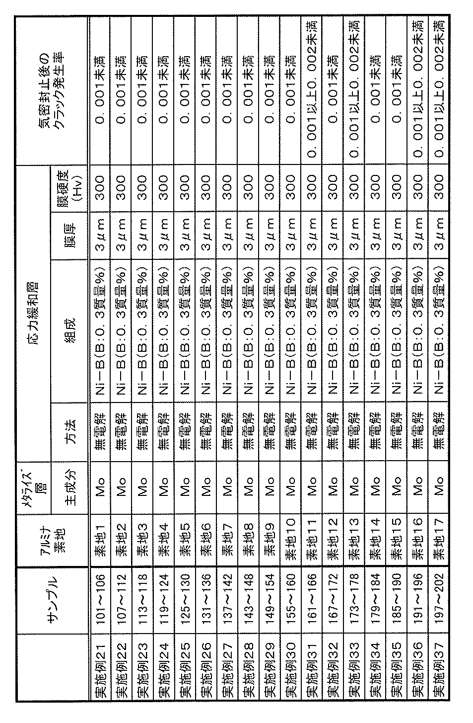
- Table 5 shows the breakdown and evaluation results (film hardness, crack occurrence rate after hermetic sealing) of Examples 21 to 37.
- Examples 21 to 30, 32, 34 and 35 using the substrates 1 to 10, 12, 14 and 15 having a bending strength of 500 MPa are all cracked as in Example 3 of the first example. The incidence was less than 0.001 and was very good.
- Examples 31, 33, 36 and 37 using the substrates 11, 13, 16 and 17 having a bending strength of less than 500 MPa have a crack occurrence rate of 0.001 or more and less than 0.002, which is not good. However, it was higher than the other examples.
- Example 41 The substrate 1 is used as the ceramic substrate, the paste 1 is used as the conductor paste, the composition of the stress relaxation layer 28 is Ni—P (P is 1.0 mass%), and 625 in accordance with the manufacturing method shown in FIG. Samples 211 were produced. The thickness of the stress relaxation layer 28 was 3 ⁇ m. Similarly, 625 samples 212 to 216 were produced using pastes 2 to 6 as conductor pastes, respectively. This was designated as Example 41. This Example 41 is the same as Example 11 in the first example.
- Example 42 to 57 were produced in the same manner as in Example 41 except that the ceramic substrate to be used was changed.
- the ceramic substrates used were the substrates 2 to 17 in Examples 42 to 57.
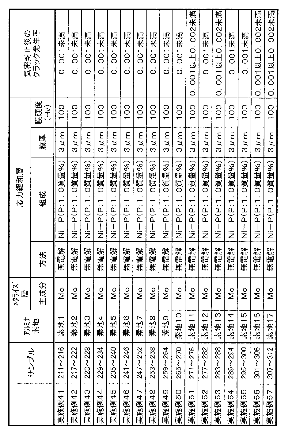
- Table 6 shows the breakdown and evaluation results (film hardness, crack occurrence rate after hermetic sealing) of Examples 41 to 57.
- Examples 41 to 50, 52, 54 and 55 using the substrates 1 to 10, 12, 14 and 15 having a bending strength of 500 MPa are all cracked as in Example 10 of the first example. The incidence was less than 0.001 and was very good. On the other hand, Examples 51, 53, 56 and 57 using the substrates 11, 13, 16 and 17 having a bending strength of less than 500 MPa have a crack generation rate of 0.001 or more and less than 0.002, which is not good. However, it was higher than the other examples.
- the ceramic package and the electronic component according to the present invention are not limited to the above-described embodiments, and various configurations can be adopted without departing from the gist of the present invention.
Landscapes
- Piezo-Electric Or Mechanical Vibrators, Or Delay Or Filter Circuits (AREA)
- Ceramic Products (AREA)
Abstract
Description
先ず、以下に示す第1実施例~第3実施例を実施するにあたって、容器12を構成する複数種のセラミック素地(素地1~17)を準備した。
原料粉末は、平均粒径1.5μmのAl2O3粉末、平均粒径0.5μmのMgO粉末、平均粒径4.0μmのSiO2粉末、平均粒径3.0μmのMnCO3粉末及び平均粒径0.25μmのTiO2粉末である。
原料粉末のうち、Al2O3粉末を92.7質量%、SiO2粉末を3.0質量%、MnCO3粉末を3.5質量%、TiO2粉末を0.8質量%とし、SiO2/MnCO3を、SiO2/MnO換算で1.39とし、焼成温度を1350℃とした点以外は、上述した素地1と同様にして素地2を作製した。
原料粉末のうち、MnCO3粉末の平均粒径を1.0μmとした点以外は、上述した素地1と同様にして素地3を作製した。
原料粉末のうち、Al2O3粉末を94.5質量%、SiO2粉末を2.0質量%、MnCO3粉末を2.4質量%、TiO2粉末を0.5質量%とし、SiO2/MnCO3を、SiO2/MnO換算で1.35とし、焼成温度を1380℃とした点以外は、上述した素地1と同様にして素地4を作製した。
原料粉末のうち、Al2O3粉末を90.2質量%、MgO粉末を0.10質量%とした点以外は、上述した素地1と同様にして素地5を作製した。
原料粉末のうち、Al2O3粉末を90.9質量%、TiO2粉末を0.1質量%とした点以外は、上述した素地1と同様にして素地6を作製した。
原料粉末のうち、Al2O3粉末を87.6質量%、SiO2粉末を5.0質量%、MnCO3粉末を5.9質量%、TiO2粉末を1.2質量%とし、SiO2/MnCO3を、SiO2/MnO換算で1.37とし、焼成温度を1280℃とした点以外は、上述した素地1と同様にして素地7を作製した。
原料粉末のうち、Al2O3粉末を85.1質量%、SiO2粉末を6.0質量%、MnCO3粉末を7.1質量%、TiO2粉末を1.5質量%とし、SiO2/MnCO3を、SiO2/MnO換算で1.37とし、焼成温度を1250℃とした点以外は、上述した素地1と同様にして素地8を作製した。
原料粉末のうち、Al2O3粉末を89.3質量%、TiO2粉末を2.0質量%とした点以外は、上述した素地1と同様にして素地9を作製した。
原料粉末のうち、Al2O3粉末を89.7質量%、MgO粉末を0.60質量%とし、焼成温度を1310℃とした点以外は、上述した素地1と同様にして素地10を作製した。
原料粉末のうち、Al2O3粉末を94.0質量%、MgO粉末を3.00質量%、SiO2粉末を3.0質量%、MnCO3粉末を0.0質量%、TiO2粉末を0.0質量%とし、焼成温度を1350℃とした点以外は、上述した素地1と同様にして素地11を作製した。
原料粉末のうち、Al2O3粉末を92.0質量%、MgO粉末を0.34質量%、SiO2粉末を3.4質量%、MnCO3粉末を6.4質量%、TiO2粉末を0.0質量%とし、SiO2/MnCO3を、SiO2/MnO換算で0.87とした点以外は、上述した素地1と同様にして素地12を作製した。
原料粉末のうち、Al2O3粉末を90.2質量%、MgO粉末を0.34質量%、SiO2粉末を4.4質量%、MnCO3粉末を5.0質量%、TiO2粉末を0.0質量%とし、SiO2/MnCO3を、SiO2/MnO換算で1.43とした点以外は、上述した素地1と同様にして素地13を作製した。
原料粉末のうち、Al2O3粉末を88.4質量%、SiO2粉末を2.9質量%、MnCO3粉末を8.5質量%、TiO2粉末を0.0質量%とし、SiO2/MnCO3を、SiO2/MnO換算で0.55とした点以外は、上述した素地1と同様にして素地14を作製した。
原料粉末のうち、Al2O3粉末を88.4質量%、SiO2粉末を2.9質量%、MnCO3粉末を8.5質量%とし、SiO2/MnCO3を、SiO2/MnO換算で0.55とした点以外は、上述した素地1と同様にして素地15を作製した。
原料粉末のうち、TiO2粉末を0.0質量%とした点以外は、上述した素地1と同様にして素地16を作製した。
原料粉末のうち、Al2O3粉末を91.3質量%、MgO粉末を0.00質量%、とした点以外は、上述した素地1と同様にして素地17を作製した。
(結晶相の確認)
素地1~17をX線回折により同定した。
素地1~17を、媒体を水とするアルキメデス法にて測定した。
素地1~17を、JISR1601の4点曲げ強度試験に基づいて室温にて測定した。
以下に示す第1実施例~第3実施例を実施するにあたって、メタライズ層を形成するための複数種の導体ペースト(ペースト1~6)を準備した。金属粉末及び添加物の混合割合を下記表3に示す。なお、共素地粉末は、上述した素地1~17のうち、使用するセラミック素地と同等の粉末をいう。
実施例1~12、比較例1~3について、同種のセラミック素地を使用し、応力緩和層の主成分(Ni)に対する添加物(B又はP)の割合を変えたときの膜硬度の変化並びに気密封止後のクラック発生率を確認した。
セラミック素地として素地1を使用し、導体ペーストとしてペースト1を使用し、応力緩和層28の組成をNi-B(Bを0.9質量%)として、図2に示す製造方法に準拠して625個のサンプル1を作製した。高温封止材16として、上述した表1のろう材3を使用した。また、応力緩和層28の膜厚を3μmとした。同様にして、導体ペーストとしてペースト2~6を使用して、それぞれ625個のサンプル2~6を作製した。これを実施例1とした。
実施例1と同様にして、応力緩和層28の組成Ni-BのBの添加量を変えて、実施例2(サンプル7~12)、実施例3(サンプル13~18)、実施例4(サンプル19~24)、実施例5(サンプル25~30)、実施例6(サンプル31~36)を作製した。ここで、Bの添加量は、実施例2が0.5質量%、実施例3が0.3質量%、実施例4が0.1質量%、実施例5が0.05質量%、実施例6が0.01質量%である。
応力緩和層28の組成をNi-P(Pを7.0質量%)とした点以外は、実施例1と同様にしてサンプル37~42を作製した。
実施例7と同様にして、応力緩和層28の組成Ni-PのPの添加量を変えて、実施例8(サンプル43~48)、実施例9(サンプル49~54)、実施例10(サンプル55~60)、実施例11(サンプル61~66)、実施例12(サンプル67~72)を作製した。ここで、Pの添加量は、実施例8が5.0質量%、実施例9が3.0質量%、実施例10が1.5質量%、実施例11が1.0質量%、実施例12が0.01質量%である。
応力緩和層28の組成をNi-B(Bを3.0質量%)とした点以外は、実施例1と同様にしてサンプル73~78を作製した。
応力緩和層28の組成をNi-B(Bを1.0質量%)とした点以外は、実施例1と同様にしてサンプル79~84を作製した。
応力緩和層28の組成をNi-P(Pを8.0質量%)とした点以外は、実施例10と同様にしてサンプル85~90を作製した。
(膜硬度)
実施例1~12、比較例1~3の各サンプルにおける応力緩和層28の膜硬度(ビッカース硬さ)を、JISZ2252の超微小負荷硬さ試験方法に基づいて室温にて測定した。
実施例1~12、比較例1~3の各サンプルにつき、625個のセラミックパッケージをHe(ヘリウム)ガスでのリーク検査を行い、さらに、接合部の断面検査での、めっき部及びセラミック部分のクラックの有無を検査した。場合によっては、接合部を平面方向から研磨し、めっき部分及びメタライズ層直下のセラミック部分のクラックの有無を検査した。例えば実施例1についてみると、サンプル1~6における全セラミックパッケージ、すなわち、625×6=3750個のセラミックパッケージについて、クラックの発生の有無を検査した。
実施例21~37について、応力緩和層28の主成分(Ni)に対する添加物(B)の割合を同じにし、使用するセラミック素地を変えたときの気密封止後のクラック発生率を確認した。
セラミック素地として素地1を使用し、導体ペーストとしてペースト1を使用し、応力緩和層28の組成をNi-B(Bを0.3質量%)として、図2に示す製造方法に準拠して625個のサンプル101を作製した。応力緩和層28の膜厚を3μmとした。同様にして、導体ペーストとしてペースト2~6を使用して、それぞれ625個のサンプル102~106を作製した。これを実施例21とした。この実施例21は、第1実施例における実施例3と同じである。
使用するセラミック素地を変えたこと以外は、実施例21と同様にして、実施例22~37を作製した。ここで、使用するセラミック素地は、実施例22~37について、素地2~17とした。
実施例41~57について、応力緩和層28の主成分(Ni)に対する添加物(P)の割合を同じにし、使用するセラミック素地を変えたときの気密封止後のクラック発生率を確認した。
セラミック素地として素地1を使用し、導体ペーストとしてペースト1を使用し、応力緩和層28の組成をNi-P(Pを1.0質量%)として、図2に示す製造方法に準拠して625個のサンプル211を作製した。応力緩和層28の膜厚を3μmとした。同様にして、導体ペーストとしてペースト2~6を使用して、それぞれ625個のサンプル212~216を作製した。これを実施例41とした。この実施例41は、第1実施例における実施例11と同じである。
使用するセラミック素地を変えたこと以外は、実施例41と同様にして、実施例42~57を作製した。ここで、使用するセラミック素地は、実施例42~57について、素地2~17とした。
Claims (11)
- 底部(12a)と側壁(12b)とを有する上面開口のセラミック製の容器(12)と、該容器(12)の前記開口を閉塞する蓋(14)とが高温封止材(16)を用いて封止されたセラミックパッケージにおいて、
前記容器(12)における前記側壁(12b)の上端面と前記高温封止材(16)との間に接合層(24)を有し、
前記接合層(24)は、
前記側壁(12b)の上端面に形成されたメタライズ層(26)と、
前記メタライズ層(26)上に形成された応力緩和層(28)とを有し、
前記応力緩和層(28)は、
膜硬度(ビッカース硬さ)が50以上500未満の無電解めっき層であることを特徴とするセラミックパッケージ。 - 請求項1記載のセラミックパッケージにおいて、
前記応力緩和層(28)は、
ニッケルを主成分とする無電解めっき層であることを特徴とするセラミックパッケージ。 - 請求項2記載のセラミックパッケージにおいて、
前記応力緩和層(28)は、
前記ニッケルに、ボロンが0.01質量%以上1.0質量%未満含有された無電解めっき層であることを特徴とするセラミックパッケージ。 - 請求項2記載のセラミックパッケージにおいて、
前記応力緩和層(28)は、
前記ニッケルに、ボロンが0.01質量%以上0.3質量%以下含有された無電解めっき層であることを特徴とするセラミックパッケージ。 - 請求項2記載のセラミックパッケージにおいて、
前記応力緩和層(28)は、
前記ニッケルに、リンが0.01質量%以上8質量%未満含有された無電解めっき層であることを特徴とするセラミックパッケージ。 - 請求項2記載のセラミックパッケージにおいて、
前記応力緩和層(28)は、
前記ニッケルに、リンが0.01質量%以上1.5質量%以下含有された無電解めっき層であることを特徴とするセラミックパッケージ。 - 請求項1~6のいずれか1項に記載のセラミックパッケージにおいて、
前記容器(12)は、曲げ強度が500MPa以上のセラミック素地にて形成されていることを特徴とするセラミックパッケージ。 - 請求項7記載のセラミックパッケージにおいて、
前記セラミック素地は、Al2O3を主結晶相とし、その他、MnTiO3結晶相、MnAl2O4結晶相を含み、比重が3.6よりも大きいことを特徴とするセラミックパッケージ。 - 請求項1~8のいずれか1項に記載のセラミックパッケージにおいて、
前記接合層(24)は、さらに、前記応力緩和層(28)と前記高温封止材(16)との間に少なくとも貴金属の無電解めっき層(30)が介在されていることを特徴とするセラミックパッケージ。 - 請求項9記載のセラミックパッケージにおいて、
前記応力緩和層(28)は、前記貴金属の無電解めっき層(30)と共に、前記高温封止材(16)の濡れ性を向上させる層として機能することを特徴とするセラミックパッケージ。 - 請求項1~10のいずれか1項に記載のセラミックパッケージと、
前記セラミックパッケージの前記容器(12)内に封止された素子(20)とを有することを特徴とする電子部品。
Priority Applications (2)
| Application Number | Priority Date | Filing Date | Title |
|---|---|---|---|
| JP2015506785A JP6406646B2 (ja) | 2013-03-21 | 2014-03-18 | セラミックパッケージ及び電子部品 |
| CN201480017049.6A CN105051889B (zh) | 2013-03-21 | 2014-03-18 | 陶瓷封装体及电子器件 |
Applications Claiming Priority (2)
| Application Number | Priority Date | Filing Date | Title |
|---|---|---|---|
| JP2013-058173 | 2013-03-21 | ||
| JP2013058173 | 2013-03-21 |
Publications (1)
| Publication Number | Publication Date |
|---|---|
| WO2014148457A1 true WO2014148457A1 (ja) | 2014-09-25 |
Family
ID=51580136
Family Applications (1)
| Application Number | Title | Priority Date | Filing Date |
|---|---|---|---|
| PCT/JP2014/057225 Ceased WO2014148457A1 (ja) | 2013-03-21 | 2014-03-18 | セラミックパッケージ及び電子部品 |
Country Status (3)
| Country | Link |
|---|---|
| JP (1) | JP6406646B2 (ja) |
| CN (1) | CN105051889B (ja) |
| WO (1) | WO2014148457A1 (ja) |
Cited By (3)
| Publication number | Priority date | Publication date | Assignee | Title |
|---|---|---|---|---|
| JP2016072321A (ja) * | 2014-09-29 | 2016-05-09 | 日本特殊陶業株式会社 | セラミック基板 |
| JP2016139758A (ja) * | 2015-01-29 | 2016-08-04 | 株式会社日立金属ネオマテリアル | 気密封止用蓋材および電子部品収容パッケージ |
| KR20210030408A (ko) | 2018-07-10 | 2021-03-17 | 니폰 덴키 가라스 가부시키가이샤 | 패키지, 패키지 제조 방법, 접합재가 부착된 덮개체, 및 접합재가 부착된 덮개체의 제조 방법 |
Families Citing this family (2)
| Publication number | Priority date | Publication date | Assignee | Title |
|---|---|---|---|---|
| JP2017204544A (ja) * | 2016-05-10 | 2017-11-16 | 太陽誘電株式会社 | 電子デバイスおよびその製造方法 |
| CN114634369A (zh) * | 2020-12-15 | 2022-06-17 | 中国科学院大连化学物理研究所 | 一种可在高温氧化和还原气氛下长期使用的陶瓷密封方法 |
Citations (4)
| Publication number | Priority date | Publication date | Assignee | Title |
|---|---|---|---|---|
| JPH0769750A (ja) * | 1993-06-29 | 1995-03-14 | Tokuyama Corp | セラミック接合構造体 |
| JPH1174392A (ja) * | 1997-08-28 | 1999-03-16 | Kyocera Corp | 電子部品収納用パッケージ |
| JP2003105549A (ja) * | 2001-09-28 | 2003-04-09 | Kyocera Corp | 配線基板およびその製造方法 |
| JP2003309226A (ja) * | 2002-02-14 | 2003-10-31 | Kyocera Corp | セラミックパッケージ及びその製造方法 |
Family Cites Families (1)
| Publication number | Priority date | Publication date | Assignee | Title |
|---|---|---|---|---|
| CN201677551U (zh) * | 2010-05-21 | 2010-12-22 | 中国电子科技集团公司第十三研究所 | 氮化铝陶瓷与金属的焊接结构 |
-
2014
- 2014-03-18 CN CN201480017049.6A patent/CN105051889B/zh active Active
- 2014-03-18 WO PCT/JP2014/057225 patent/WO2014148457A1/ja not_active Ceased
- 2014-03-18 JP JP2015506785A patent/JP6406646B2/ja active Active
Patent Citations (4)
| Publication number | Priority date | Publication date | Assignee | Title |
|---|---|---|---|---|
| JPH0769750A (ja) * | 1993-06-29 | 1995-03-14 | Tokuyama Corp | セラミック接合構造体 |
| JPH1174392A (ja) * | 1997-08-28 | 1999-03-16 | Kyocera Corp | 電子部品収納用パッケージ |
| JP2003105549A (ja) * | 2001-09-28 | 2003-04-09 | Kyocera Corp | 配線基板およびその製造方法 |
| JP2003309226A (ja) * | 2002-02-14 | 2003-10-31 | Kyocera Corp | セラミックパッケージ及びその製造方法 |
Cited By (3)
| Publication number | Priority date | Publication date | Assignee | Title |
|---|---|---|---|---|
| JP2016072321A (ja) * | 2014-09-29 | 2016-05-09 | 日本特殊陶業株式会社 | セラミック基板 |
| JP2016139758A (ja) * | 2015-01-29 | 2016-08-04 | 株式会社日立金属ネオマテリアル | 気密封止用蓋材および電子部品収容パッケージ |
| KR20210030408A (ko) | 2018-07-10 | 2021-03-17 | 니폰 덴키 가라스 가부시키가이샤 | 패키지, 패키지 제조 방법, 접합재가 부착된 덮개체, 및 접합재가 부착된 덮개체의 제조 방법 |
Also Published As
| Publication number | Publication date |
|---|---|
| CN105051889B (zh) | 2018-10-16 |
| JP6406646B2 (ja) | 2018-10-17 |
| CN105051889A (zh) | 2015-11-11 |
| JPWO2014148457A1 (ja) | 2017-02-16 |
Similar Documents
| Publication | Publication Date | Title |
|---|---|---|
| US20140196934A1 (en) | Wiring substrate and electronic device | |
| JP5902292B2 (ja) | セラミック素地及びその製造方法 | |
| JP6406646B2 (ja) | セラミックパッケージ及び電子部品 | |
| CN107409472B (zh) | 配线基板 | |
| CN107001147B (zh) | 陶瓷基体及其制造方法 | |
| JP5293605B2 (ja) | セラミック多層基板及びその製造方法 | |
| JP6314292B1 (ja) | セラミック素地及びその製造方法 | |
| CN106458761B (zh) | 陶瓷基体及其制造方法 | |
| JP6581967B2 (ja) | セラミック素地及びその製造方法 | |
| CN105470208B (zh) | 陶瓷基板 | |
| JP6195479B2 (ja) | 多層セラミック基板およびその製造方法 | |
| JP6640112B2 (ja) | セラミック素地及びその製造方法 | |
| JPH09263472A (ja) | 配線基板 | |
| JP2000191385A (ja) | 半導体素子収納用パッケ―ジ |
Legal Events
| Date | Code | Title | Description |
|---|---|---|---|
| WWE | Wipo information: entry into national phase |
Ref document number: 201480017049.6 Country of ref document: CN |
|
| 121 | Ep: the epo has been informed by wipo that ep was designated in this application |
Ref document number: 14770126 Country of ref document: EP Kind code of ref document: A1 |
|
| ENP | Entry into the national phase |
Ref document number: 2015506785 Country of ref document: JP Kind code of ref document: A |
|
| NENP | Non-entry into the national phase |
Ref country code: DE |
|
| 122 | Ep: pct application non-entry in european phase |
Ref document number: 14770126 Country of ref document: EP Kind code of ref document: A1 |