WO2014148407A1 - 透明導電体 - Google Patents
透明導電体 Download PDFInfo
- Publication number
- WO2014148407A1 WO2014148407A1 PCT/JP2014/057042 JP2014057042W WO2014148407A1 WO 2014148407 A1 WO2014148407 A1 WO 2014148407A1 JP 2014057042 W JP2014057042 W JP 2014057042W WO 2014148407 A1 WO2014148407 A1 WO 2014148407A1
- Authority
- WO
- WIPO (PCT)
- Prior art keywords
- silver
- transparent conductor
- transparent
- underlayer
- polymer
- Prior art date
- Legal status (The legal status is an assumption and is not a legal conclusion. Google has not performed a legal analysis and makes no representation as to the accuracy of the status listed.)
- Ceased
Links
Images

Classifications
-
- C—CHEMISTRY; METALLURGY
- C23—COATING METALLIC MATERIAL; COATING MATERIAL WITH METALLIC MATERIAL; CHEMICAL SURFACE TREATMENT; DIFFUSION TREATMENT OF METALLIC MATERIAL; COATING BY VACUUM EVAPORATION, BY SPUTTERING, BY ION IMPLANTATION OR BY CHEMICAL VAPOUR DEPOSITION, IN GENERAL; INHIBITING CORROSION OF METALLIC MATERIAL OR INCRUSTATION IN GENERAL
- C23C—COATING METALLIC MATERIAL; COATING MATERIAL WITH METALLIC MATERIAL; SURFACE TREATMENT OF METALLIC MATERIAL BY DIFFUSION INTO THE SURFACE, BY CHEMICAL CONVERSION OR SUBSTITUTION; COATING BY VACUUM EVAPORATION, BY SPUTTERING, BY ION IMPLANTATION OR BY CHEMICAL VAPOUR DEPOSITION, IN GENERAL
- C23C18/00—Chemical coating by decomposition of either liquid compounds or solutions of the coating forming compounds, without leaving reaction products of surface material in the coating; Contact plating
- C23C18/16—Chemical coating by decomposition of either liquid compounds or solutions of the coating forming compounds, without leaving reaction products of surface material in the coating; Contact plating by reduction or substitution, e.g. electroless plating
- C23C18/31—Coating with metals
- C23C18/42—Coating with noble metals
- C23C18/44—Coating with noble metals using reducing agents
-
- C—CHEMISTRY; METALLURGY
- C08—ORGANIC MACROMOLECULAR COMPOUNDS; THEIR PREPARATION OR CHEMICAL WORKING-UP; COMPOSITIONS BASED THEREON
- C08J—WORKING-UP; GENERAL PROCESSES OF COMPOUNDING; AFTER-TREATMENT NOT COVERED BY SUBCLASSES C08B, C08C, C08F, C08G or C08H
- C08J7/00—Chemical treatment or coating of shaped articles made of macromolecular substances
- C08J7/04—Coating
- C08J7/042—Coating with two or more layers, where at least one layer of a composition contains a polymer binder
- C08J7/0423—Coating with two or more layers, where at least one layer of a composition contains a polymer binder with at least one layer of inorganic material and at least one layer of a composition containing a polymer binder
-
- C—CHEMISTRY; METALLURGY
- C08—ORGANIC MACROMOLECULAR COMPOUNDS; THEIR PREPARATION OR CHEMICAL WORKING-UP; COMPOSITIONS BASED THEREON
- C08J—WORKING-UP; GENERAL PROCESSES OF COMPOUNDING; AFTER-TREATMENT NOT COVERED BY SUBCLASSES C08B, C08C, C08F, C08G or C08H
- C08J7/00—Chemical treatment or coating of shaped articles made of macromolecular substances
- C08J7/04—Coating
- C08J7/043—Improving the adhesiveness of the coatings per se, e.g. forming primers
-
- C—CHEMISTRY; METALLURGY
- C08—ORGANIC MACROMOLECULAR COMPOUNDS; THEIR PREPARATION OR CHEMICAL WORKING-UP; COMPOSITIONS BASED THEREON
- C08J—WORKING-UP; GENERAL PROCESSES OF COMPOUNDING; AFTER-TREATMENT NOT COVERED BY SUBCLASSES C08B, C08C, C08F, C08G or C08H
- C08J7/00—Chemical treatment or coating of shaped articles made of macromolecular substances
- C08J7/04—Coating
- C08J7/044—Forming conductive coatings; Forming coatings having anti-static properties
-
- C—CHEMISTRY; METALLURGY
- C23—COATING METALLIC MATERIAL; COATING MATERIAL WITH METALLIC MATERIAL; CHEMICAL SURFACE TREATMENT; DIFFUSION TREATMENT OF METALLIC MATERIAL; COATING BY VACUUM EVAPORATION, BY SPUTTERING, BY ION IMPLANTATION OR BY CHEMICAL VAPOUR DEPOSITION, IN GENERAL; INHIBITING CORROSION OF METALLIC MATERIAL OR INCRUSTATION IN GENERAL
- C23C—COATING METALLIC MATERIAL; COATING MATERIAL WITH METALLIC MATERIAL; SURFACE TREATMENT OF METALLIC MATERIAL BY DIFFUSION INTO THE SURFACE, BY CHEMICAL CONVERSION OR SUBSTITUTION; COATING BY VACUUM EVAPORATION, BY SPUTTERING, BY ION IMPLANTATION OR BY CHEMICAL VAPOUR DEPOSITION, IN GENERAL
- C23C18/00—Chemical coating by decomposition of either liquid compounds or solutions of the coating forming compounds, without leaving reaction products of surface material in the coating; Contact plating
- C23C18/16—Chemical coating by decomposition of either liquid compounds or solutions of the coating forming compounds, without leaving reaction products of surface material in the coating; Contact plating by reduction or substitution, e.g. electroless plating
- C23C18/1601—Process or apparatus
- C23C18/1633—Process of electroless plating
- C23C18/1646—Characteristics of the product obtained
- C23C18/165—Multilayered product
-
- C—CHEMISTRY; METALLURGY
- C23—COATING METALLIC MATERIAL; COATING MATERIAL WITH METALLIC MATERIAL; CHEMICAL SURFACE TREATMENT; DIFFUSION TREATMENT OF METALLIC MATERIAL; COATING BY VACUUM EVAPORATION, BY SPUTTERING, BY ION IMPLANTATION OR BY CHEMICAL VAPOUR DEPOSITION, IN GENERAL; INHIBITING CORROSION OF METALLIC MATERIAL OR INCRUSTATION IN GENERAL
- C23C—COATING METALLIC MATERIAL; COATING MATERIAL WITH METALLIC MATERIAL; SURFACE TREATMENT OF METALLIC MATERIAL BY DIFFUSION INTO THE SURFACE, BY CHEMICAL CONVERSION OR SUBSTITUTION; COATING BY VACUUM EVAPORATION, BY SPUTTERING, BY ION IMPLANTATION OR BY CHEMICAL VAPOUR DEPOSITION, IN GENERAL
- C23C18/00—Chemical coating by decomposition of either liquid compounds or solutions of the coating forming compounds, without leaving reaction products of surface material in the coating; Contact plating
- C23C18/16—Chemical coating by decomposition of either liquid compounds or solutions of the coating forming compounds, without leaving reaction products of surface material in the coating; Contact plating by reduction or substitution, e.g. electroless plating
- C23C18/1601—Process or apparatus
- C23C18/1633—Process of electroless plating
- C23C18/1655—Process features
-
- C—CHEMISTRY; METALLURGY
- C08—ORGANIC MACROMOLECULAR COMPOUNDS; THEIR PREPARATION OR CHEMICAL WORKING-UP; COMPOSITIONS BASED THEREON
- C08J—WORKING-UP; GENERAL PROCESSES OF COMPOUNDING; AFTER-TREATMENT NOT COVERED BY SUBCLASSES C08B, C08C, C08F, C08G or C08H
- C08J2367/00—Characterised by the use of polyesters obtained by reactions forming a carboxylic ester link in the main chain; Derivatives of such polymers
- C08J2367/02—Polyesters derived from dicarboxylic acids and dihydroxy compounds
Definitions
- the present invention relates to a transparent conductor. More specifically, the present invention relates to a transparent conductor having low surface resistance and high light transmittance.
- Transparent conductors are used in electrode materials for display devices such as liquid crystal displays, plasma displays, inorganic and organic electroluminescence (EL) displays, electrode materials for inorganic and organic EL elements, touch panels and solar cells. .
- display devices such as liquid crystal displays, plasma displays, inorganic and organic electroluminescence (EL) displays, electrode materials for inorganic and organic EL elements, touch panels and solar cells. .
- EL electroluminescence
- a transparent conductor As a material constituting such a transparent conductor, gold (Au), silver (Ag), platinum (Pt), copper (Cu), rhodium (Rh), palladium (Pd), aluminum (Al), chromium (Cr ) And other metals, indium oxide (In 2 O 3 ), cadmium oxide (CdO), cadmium indium oxide (CdIn 2 O 4 ), cadmium tin oxide (Cd 2 SnO 4 ), titanium oxide (TiO 2 ), oxidation Oxide semiconductors such as tin (SnO 2 ) and zinc oxide (ZnO) are known. Among these, a transparent conductor made of an indium tin oxide (ITO) film is frequently used from the viewpoint of light transmittance and conductivity.
- ITO indium tin oxide
- a transparent conductor in which silver is arranged in a mesh shape has been proposed as a transparent conductor that replaces the ITO film (see, for example, Patent Document 1).
- the transparent conductive film disclosed in Patent Document 1 has a silver mesh width of about 20 ⁇ m. Therefore, the silver mesh is easily visible and cannot be applied to uses where high transparency is required. Furthermore, although there is conduction in the mesh portion, it is not sufficiently conducted in the gap portion of the mesh, and the surface resistance cannot be lowered sufficiently.
- a transparent conductor containing silver nanowires has been proposed (see, for example, Patent Document 2).
- the transparent conductive film has a large surface resistance, and the thickness of the transparent conductive film needs to be about 200 nm. For this reason, it is difficult to apply the transparent conductor to applications that require flexibility.
- Non-Patent Document 1 A transparent conductor in which a niobium oxide (Nb 2 O 5 ) film, a silver film, and an indium zinc oxide (IZO) film are stacked has also been proposed (see, for example, Non-Patent Document 1).
- the present invention has been made in view of the above-mentioned problems and situations, and a problem to be solved is to provide a transparent conductor having low surface resistance and high light transmittance.
- the present inventor can solve the problem by providing a silver layer and an underlayer containing a specific polymer having a sulfur atom adjacent to each other. And found the present invention.
- an underlayer containing a polymer having a sulfur atom and a weight average molecular weight in the range of 1,000 to 1,000,000, and a transparent conductive layer containing silver or a silver alloy adjacent to the underlayer A transparent conductor, comprising:
- a transparent conductor having both low surface resistance and high light transmittance can be provided.
- the specific polymer having a sulfur atom and silver or a silver alloy (hereinafter also referred to as silver or the like). Due to the action, the diffusion distance of silver or the like at the adjacent interface is reduced, and aggregation at a specific location is suppressed. Therefore, in general, a thin conductive layer containing silver or a silver alloy that is easily isolated in an island shape by film growth of an island-like growth type (Volume-Weber: VW type) is a single-layer growth type (Frank-van der Merwe (FM type) film growth is considered to be uniform.
- the transparent conductor of the present invention comprises an underlayer containing a polymer having a sulfur atom and a weight average molecular weight in the range of 1,000 to 1,000,000 on a transparent support, and silver or a silver alloy adjacent to the underlayer It has the transparent conductive layer containing this, It is characterized by the above-mentioned.
- This feature is a technical feature common to the inventions according to claims 1 to 4.
- the polymer has an aromatic ring from the viewpoint of manifesting the effect of the present invention.
- the layer thickness of the transparent conductive layer is preferably in the range of 1 to 20 nm.
- the transparent conductor preferably has a light transmittance of 80% or more at a wavelength of 550 nm.
- ⁇ is used to mean that the numerical values described before and after it are included as a lower limit value and an upper limit value.
- the transparent conductor of the present invention comprises a base layer containing a polymer having a sulfur atom and a weight average molecular weight in the range of 1,000 to 1,000,000 (hereinafter also referred to as S polymer) on a transparent support. And a transparent conductive layer containing silver or a silver alloy adjacent to the base layer.
- FIG. 1 is a schematic cross-sectional view showing an example of the configuration of the transparent conductor according to the embodiment.
- the transparent conductor 1 is a layer in which a base layer 3 and a transparent conductive layer 4 containing silver or a silver alloy formed thereon are sequentially laminated on a transparent support 2.
- the structure is a structure, and the underlayer 3 is a layer configured to contain an S polymer.
- the term “transparent” means that the light transmittance at a wavelength of 550 nm is 50% or more.
- the transparent conductor of the present invention has a light transmittance of 50% or more at a wavelength of 550 nm, and preferably has a light transmittance of 80% or more at a wavelength of 550 nm.
- the light transmittance can be measured by a known method using a spectrophotometer or the like.
- a transparent conductive layer containing silver or a silver alloy is provided adjacent to the underlayer, and the underlayer has a sulfur atom having an affinity for silver atoms. It is the structure that S polymer is contained.
- the silver atoms constituting the conductive layer interact with the S polymer contained in the underlayer, and silver on the surface of the underlayer The diffusion distance of atoms is reduced, and the aggregation of silver at specific points is suppressed.
- a silver atom first forms a two-dimensional nucleus on the surface of the underlayer containing a compound having an atom having an affinity for the silver atom, and forms a two-dimensional single crystal layer around it.
- the film is formed by the layer growth type (Frank-van der Merwe: FM type) film growth.
- an island-shaped growth type (Volume-Weber) in which silver atoms adhering to the surface of the underlayer are bonded while diffusing the surface to form a three-dimensional nucleus and grow into a three-dimensional island shape. : VW type), it is considered that the film is easily formed into an island shape.
- the S polymer contained in the underlayer prevents the island-like growth in this manner, and a single layer. It is assumed that growth will be promoted.
- a transparent conductive layer having a uniform layer thickness can be obtained even though the layer thickness is thin.
- the transparent conductive layer containing silver or a silver alloy according to the present invention includes aluminum (Al), gold (Au), In (indium), copper (Cu), palladium (Pd), platinum, which are solid solution elements with respect to silver. (Pt) can be contained. Thereby, it becomes what was comprised with the solid solution of silver and these additional elements, silver migration is suppressed, and a layer becomes uniform.
- the silver content in the transparent conductive layer containing silver or a silver alloy is 50% by mass or more, and preferably in the range of 80 to 100% by mass. More preferably, the transparent conductive layer containing silver or a silver alloy is preferably a layer made of silver.
- the layer thickness of the transparent conductive layer containing silver or a silver alloy is preferably in the range of 1 to 20 nm, more preferably in the range of 3 to 15 nm. When the layer thickness is within this range, it is preferable to achieve both high light transmittance and low surface resistance.
- the underlayer according to the present invention contains, as a main component, a polymer (S polymer) having a sulfur atom and having a weight average molecular weight in the range of 1,000 to 1,000,000.
- the main component refers to 50% by mass or more based on the total composition of the underlayer. Preferably, it is in the range of 70 to 100% by mass.
- the S polymer according to the present invention may be one kind or a plurality may be mixed. It is also permitted to mix a compound having no sulfur atom within a range that does not impair the effects of the present invention.
- the thickness of the underlayer according to the present invention can be provided in an arbitrary range from 5 nm to 1 ⁇ m, but is preferably in the range of 10 to 500 nm as a range for ensuring the uniformity of the transparent conductive layer.
- the polymer (S polymer) having a sulfur atom and a weight average molecular weight in the range of 1,000 to 1,000,000 according to the present invention has a sulfide bond, a disulfide bond, a mercapto group, a sulfone group, a thiocarbonyl bond, etc. What is necessary is just to have, and it is especially preferable that they are a sulfide bond and a mercapto group.
- the S polymer preferably has an aromatic ring.
- polymerization form of the S polymer examples include a polycondensation polymer such as polyester, an acrylic derivative monomer, a vinyl polymerization polymer composed of a styrene derivative monomer, and the like.
- specific S polymers include, for example, polymers composed of the following monomer units.
- the subscript of each monomer unit indicates the constituent ratio (molar ratio) of the copolymer.
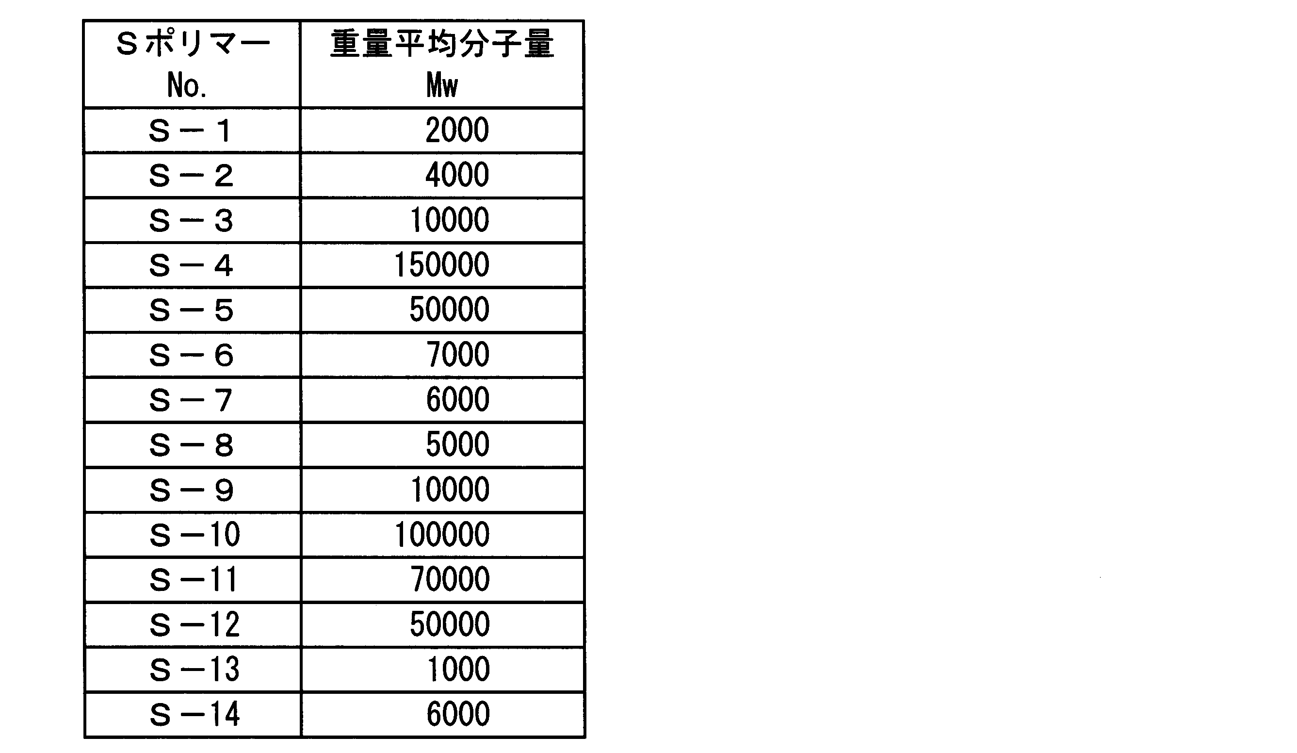
- the total molecular weight is within the range of 1,000 to 1,000,000 as shown in Table 1 as the weight average molecular weight.
- the S polymer according to the present invention can be produced by a known and well-known method.
- the weight average molecular weight can be adjusted by a well-known method such as adjusting the amount of the polymerization initiator, adjusting the reaction temperature, or introducing a polymerization terminator.
- the weight average molecular weight Mw of the S polymer according to the present invention is a value measured under the following measurement conditions at room temperature.
- Examples of the transparent support according to the present invention include glass, quartz, and a transparent resin film.
- Examples of the glass include silica glass, soda-lime silica glass, lead glass, borosilicate glass, and alkali-free glass.
- On the surface of these glass materials from the viewpoint of adhesion with the underlayer, durability, and smoothness, if necessary, physical treatment such as polishing is performed, coatings made of inorganic or organic substances, and these A hybrid coating combining the coatings may be formed.
- polyesters such as polyethylene terephthalate (PET) and polyethylene naphthalate (PEN), polyethylene, polypropylene, cellophane, cellulose diacetate, cellulose triacetate (TAC), cellulose acetate butyrate, cellulose acetate propionate ( CAP), cellulose esters such as cellulose acetate phthalate, cellulose nitrate or derivatives thereof, polyvinylidene chloride, polyvinyl alcohol, polyethylene vinyl alcohol, syndiotactic polystyrene, polycarbonate, norbornene resin, polymethylpentene, polyether ketone, polyimide , Polyethersulfone (PES), polyphenylene sulfide, polysulfones Cycloolefin resins such as polyetherimide, polyetherketoneimide, polyamide, fluororesin, nylon, polymethylmethacrylate, acrylic or polyarylate, Arton (trade name, manufactured by JSR) or Appel (trade name, manufactured by J
- the underlayer according to the present invention can be provided by a coating method, and the transparent conductive layer containing silver or a silver alloy can be provided by using a usual method such as a vapor deposition method, a sputtering method, or a coating method.
- Examples of the method for forming the underlayer include methods that can be generally used, such as a coating method (including a casting method and a spin coating method).
- the coating method is also excellent in production speed.
- the S polymer according to the present invention and other additives for example, an electron transport material, a hole transport material, etc.
- the present invention are dissolved in an appropriate solvent.
- this solution is applied on a transparent support, dried and then heat-treated.
- the solvent is not particularly limited as long as it can dissolve and disperse the S polymer, but includes alcohols such as isopropanol and n-butanol; those containing hydrogen atoms of alcohols such as hexafluoroisopropanol and tetrafluoropropanol substituted with halogen atoms.
- Alcohols such as isopropanol and n-butanol; those containing hydrogen atoms of alcohols such as hexafluoroisopropanol and tetrafluoropropanol substituted with halogen atoms.
- Halogen alcohol dimethyl sulfoxide, dimethylformamide and the like can be mentioned. These may be used individually by 1 type, and may mix and use 2 or more types.
- concentration of the S polymer in the solvent and, if necessary, the concentration of other additives is not particularly limited, but for example, the concentration in the solution is 0.005 to 0.5% by mass. Is preferred.
- the coating method is not limited, and examples thereof include spin coating, casting from a solution, dip coating, blade coating, wire bar coating, gravure coating, and spray coating. Furthermore, patterning can also be performed by a printing method such as an ink jet method, a screen printing method, a relief printing method, an intaglio printing method, an offset printing method, or a flexographic printing method.
- the heat treatment conditions after coating are not particularly limited.
- the heat treatment temperature is preferably room temperature (25 ° C.) to 180 ° C., more preferably 60 to 120 ° C.
- the heat treatment time is preferably 10 seconds to 10 minutes, more preferably 30 seconds to 5 minutes.
- polymer particles for example, latex particles
- a particle diameter of 0.01 to 0.8 ⁇ m can be used.
- Transparent conductive layer Examples of the method for forming a transparent conductive layer containing silver or a silver alloy according to the present invention include methods that can be usually used such as a vapor deposition method, a CVD method, and a coating method (including a casting method and a spin coating method).
- a method in which a transparent conductive layer is provided on the underlayer by a silver mirror reaction is preferably exemplified.
- a processing method for treating the underlayer with the active treatment liquid for silver mirror a method of applying the active treatment liquid for silver mirror to the surface on which the transparent conductive layer of the transparent support provided with the underlayer is formed, or And a method of applying an active treatment solution for silver mirror containing stannous chloride or the like to the surface of the underlayer.
- spray coating that does not select the shape of the support is particularly suitable as the coating method. Furthermore, you may wash
- Examples of the active treatment liquid for silver mirror containing stannous chloride include activation treatment liquids described in JP-A-2007-197743, JP-A-2006-274400, and the like. You may provide the process of performing the activation process by silver ion after the process processed with the active process liquid for silver mirrors.
- activation treatment with silver ions for example, treatment with a treatment solution containing silver nitrate is simple and preferable.
- the silver nitrate concentration of the silver nitrate aqueous solution used in this step is preferably 0.01 mol / L or less, and then brought into contact with the underlayer treated with stannous chloride.
- spray coating in which a new solution is always supplied is suitable.
- the silver thin film layer is formed by silver mirror reaction by mixing two liquids, an ammoniacal silver nitrate solution containing silver nitrate and ammonia, and a reducing agent solution containing a reducing agent and a strong alkali component, on the surface of the underlayer subjected to the activation treatment. Apply as is. As a result, an oxidation-reduction reaction occurs, so that metallic silver is deposited and a silver coating is formed to form a silver thin film layer.
- an aldehyde compound such as glucose or glyoxal
- an organic compound such as a hydrazine compound such as hydrazine sulfate, hydrazine carbonate or hydrazine hydrate
- an aqueous solution such as sodium sulfite or sodium thiosulfate is preferably used.
- ammoniacal silver nitrate aqueous solution several additives can be added to produce good silver.
- amino alcohol compounds such as amine, triethanolamine and triisopropanolamine
- amino acids such as glycine, alanine and sodium glycine, and salts thereof, but are not particularly limited.
- aqueous solutions are mixed in advance, and this mixed solution is applied to the surface of the underlayer using a spray gun or the like.
- Spraying method spraying method using a concentric spray gun with a structure in which two types of aqueous solutions are mixed and immediately discharged in the spray gun head, and discharging two types of aqueous solutions from a double-headed spray gun with two spray nozzles, respectively.
- spraying two kinds of aqueous solutions simultaneously using two separate spray guns. These can be arbitrarily selected according to the situation.
- a protective layer can be provided for the purpose of stabilizing the metallic silver deposited on the silver thin film layer.
- the protective layer can be subjected to a treatment such as immersion in a solution containing an organic compound having a reaction or affinity with silver, or application of the solution, but is preferably within a range not impairing the effects of the present invention.
- organic compound a well-known organic compound having an affinity for silver, such as a nitrogen-containing heterocyclic compound having a mercapto group or a thione group, is effectively used.
- the transparent conductor of the present invention includes various types of optoelectronic devices such as liquid crystal, plasma, organic electroluminescence, field emission display, touch panel, mobile phone, electronic paper, various solar cells, various electroluminescence dimming elements, etc.
- the substrate can be preferably used.
- the surface of the transparent conductor (for example, the surface on the side opposite to the transparent support material via the base layer) may be bonded to another member via the adhesive layer or the like.
- the equivalent admittance coordinates of the surface of the transparent conductor are close to the equivalent admittance coordinates of the adhesive layer.
- the equivalent admittance coordinates of the surface of the transparent conductor and the admittance coordinates of air are preferably close. Thereby, reflection of the light on the transparent conductor surface is suppressed.
- a layer for example, a TiO 2 -containing layer or a ZrO-containing layer
- a layer having a higher refractive index than that of the transparent support can be provided between the layer made of silver or the like and the transparent support.
- Transparent conductor no. 1 was prepared, the underlayer S polymer (Exemplary Compound S-1) was changed as shown in Table 2, and the others were transparent conductor Nos. 1 in the same manner as in the production of 2 to 6 were produced. Table 1 lists the weight average molecular weight of each S polymer used.
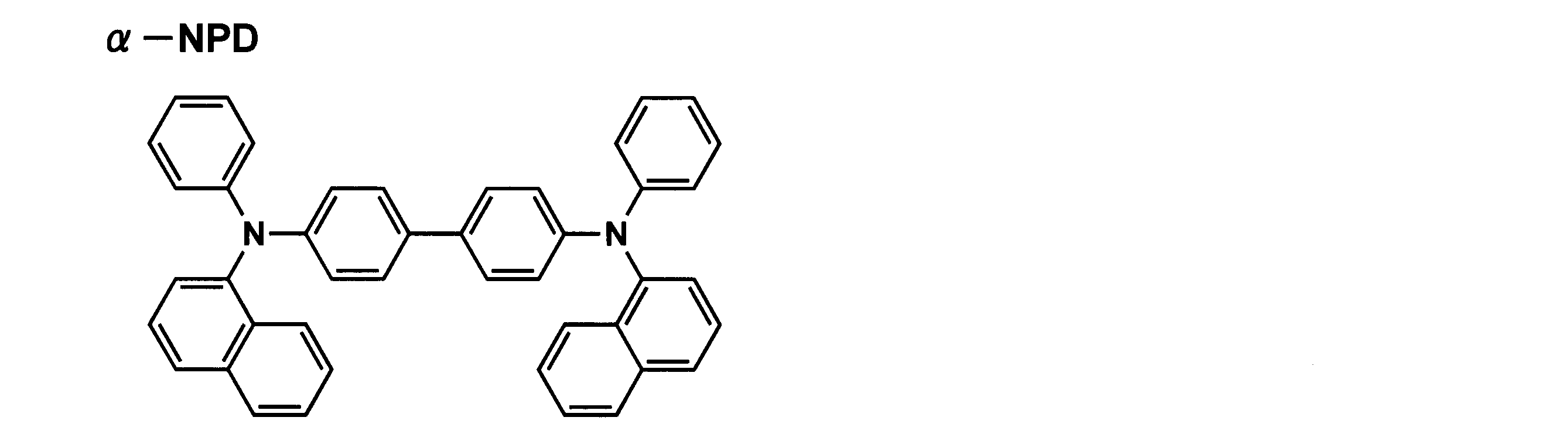
- Transparent Conductor No. 7 Preparation As a transparent conductor for comparison, transparent conductor No. In production of No. 1, ⁇ -NPD described in Patent Document 3 was provided in a thickness of 40 nm as an underlayer instead of S polymer. At this time, the degree of vacuum in the vapor deposition chamber was on the order of 10 ⁇ 5 Pa, and the film formation rate was 3 ⁇ / s. Others are transparent conductor no. 1 in the same manner as in the production of 7 was produced.
- transparent conductor No. In the production of 1, in a sample in which a conductive layer made of silver was formed without providing an underlayer, a uniform film could not be formed by electron microscope observation with an amount of silver having a thickness of 10 nm, but a uniform film at 30 nm. It was. However, the reflection was strong and there was almost no transparency.
- Table 2 shows the above evaluation results.
- sample no. 1 to 6 are comparative sample Nos. It can be seen that the surface resistance is lower than that in FIG.
- the silver mirror plating solution was prepared as follows. Separately from a silver nitrate solution in which 20 g of silver nitrate was dissolved in 10000 g of deionized water, 100 g of 28% ammonia aqueous solution and 5 g of monoethanolamine were dissolved in 10000 g of deionized water to prepare an ammonia solution. Prior to use, the silver nitrate solution and the ammonia solution were mixed one-to-one to obtain an ammoniacal silver nitrate solution. Next, 10 g of hydrazine sulfate, 5 g of monoethanolamine and 10 g of sodium hydroxide were dissolved in 10000 g of deionized water to prepare a reducing agent solution.
- the ammoniacal silver nitrate solution and the reducing agent solution thus obtained are simultaneously sprayed using a double-head spray gun so that the layer thickness after drying becomes 10 nm, to form a transparent conductive layer made of silver, and then removed. After washing with ionic water, it was dried in a dryer at 70 ° C. for 30 minutes to obtain a transparent conductor no. 11 was produced.
- Transparent Conductor No. Production of 12 to 16 >> Transparent conductor no.
- the S polymer (Exemplary Compound S-2) was changed as described in Table 3, and the others were transparent conductor No. In the same manner as the production of the transparent conductor No. 11 12 to 16 were produced.
- Table 1 lists the weight average molecular weight of each S polymer used.
- Transparent Conductor No. Preparation of No. 17 As a transparent conductor for comparison, transparent conductor No. 11 was prepared, instead of the S polymer (Exemplary Compound S-2), ⁇ -NPD described in Patent Document 3 was provided as a base layer with a thickness of 40 nm. At this time, the degree of vacuum in the vapor deposition chamber was on the order of 10 ⁇ 5 Pa, and the film formation rate was 3 ⁇ / s. Others are transparent conductor no. In the same manner as the production of the transparent conductor No. 11 17 was produced.
- sample no. 11 to 16 are comparative sample Nos. It can be seen that the surface resistance is low and the light transmittance is high compared to 17.
- the transparent conductor of the present invention includes various types of optoelectronic devices such as liquid crystal, plasma, organic electroluminescence, field emission display, touch panel, mobile phone, electronic paper, various solar cells, various electroluminescence dimming elements, etc.
- the substrate can be preferably used.
Landscapes
- Chemical & Material Sciences (AREA)
- Organic Chemistry (AREA)
- Chemical Kinetics & Catalysis (AREA)
- Polymers & Plastics (AREA)
- Medicinal Chemistry (AREA)
- Health & Medical Sciences (AREA)
- Engineering & Computer Science (AREA)
- Metallurgy (AREA)
- Mechanical Engineering (AREA)
- Materials Engineering (AREA)
- General Chemical & Material Sciences (AREA)
- Inorganic Chemistry (AREA)
- Laminated Bodies (AREA)
- Non-Insulated Conductors (AREA)
Abstract
本発明の課題は、表面抵抗が低く、かつ光透過性の高い透明導電体を提供することである。本発明の透明導電体は、透明支持体上に、硫黄原子を有し重量平均分子量が1000~1000000の範囲内であるポリマーを含有する下地層と、該下地層に隣接する銀又は銀の合金を含有する透明導電層とを有することを特徴とする。
Description
本発明は、透明導電体に関する。より詳しくは、表面抵抗が低く、かつ光透過性の高い透明導電体に関する。
液晶ディスプレイやプラズマディスプレイ、無機及び有機エレクトロルミネッセンス(EL)ディスプレイ等の表示装置の電極材料や、無機及び有機EL素子の電極材料、タッチパネル及び太陽電池等の各種装置に透明導電体が使用されている。
このような透明導電体を構成する材料として、金(Au)、銀(Ag)、白金(Pt)、銅(Cu)、ロジウム(Rh)、パラジウム(Pd)、アルミニウム(Al)、クロム(Cr)等の金属や酸化インジウム(In2O3)、酸化カドミウム(CdO)、カドミウムインジウム酸化物(CdIn2O4)、カドミウムスズ酸化物(Cd2SnO4)、酸化チタン(TiO2)、酸化スズ(SnO2)、酸化亜鉛(ZnO)等の酸化物半導体が知られている。これらの中でも、光透過性及び導電性の観点から、インジウムスズ酸化物(ITO)膜からなる透明導電体が多用されている。
近年、静電容量方式のタッチパネルが開発され、この方式では、表面抵抗が低く、かつ透明性の高い透明導電体が求められている。しかし、ITO膜では、表面抵抗を十分に低くすることが難しい。また、ITO膜は割れやすく、フレキシブル性が求められる用途に適用できない、という問題もある。
そこで、ITO膜に代わる透明導電体として、銀をメッシュ状に配置した透明導電体が提案されている(例えば、特許文献1参照。)。しかし、特許文献1に開示されている透明導電膜は、銀メッシュの幅が20μm程度である。そのため、銀メッシュが視認されやすく、高い透明性が必要とされる用途には適用できない。さらに、メッシュ部分では導通があるが、メッシュの隙間部分では十分に導通せず、表面抵抗を十分に下げることができない。
また、銀ナノワイヤを含む透明導電体も提案されている(例えば、特許文献2参照。)。しかし、当該透明導電膜は表面抵抗が大きく、透明導電膜の厚さを200nm程度にする必要がある。そのため、透明導電体をフレキシブル性が求められる用途に適用することは難しい。
さらに、銀薄膜を透明導電体とすることも提案されている(例えば、特許文献3参照。)。しかし、銀薄膜は、低い表面抵抗と、高い光透過性とを両立させることが難しい。表面抵抗を低くするために、銀薄膜の厚さを厚くすると、銀本来の反射が生じ、光透過率が低くなる。一方、光透過率を高めるために、銀薄膜を薄くすると、十分な導通が得られない。
また、さらにプラズモン吸収が生じて、透明導電膜の透過率が低くなる。なお、酸化ニオブ(Nb2O5)膜と、銀膜と、インジウム亜鉛酸化物(IZO)膜とを積層した透明導電体も提案されている(例えば、非特許文献1参照。)。
SID 2012 DIGEST p.352-353
本発明は、上記問題・状況に鑑みてなされたものであり、その解決課題は、表面抵抗が低く、かつ光透過性の高い透明導電体を提供することである。
本発明者は、上記課題を解決すべく、上記問題の原因等について検討した結果、銀層と硫黄原子を有する特定のポリマーを含有する下地層とを隣接して設けることで、問題を解決できることを見出し本発明に至った。
すなわち、本発明に係る上記課題は、以下の手段により解決される。
1.透明支持体上に、硫黄原子を有し重量平均分子量が1000~1000000の範囲内であるポリマーを含有する下地層と、該下地層に隣接する銀又は銀の合金を含有する透明導電層とを有することを特徴とする透明導電体。
2.前記ポリマーが、芳香族環を有することを特徴とする第1項に記載の透明導電体。
3.前記透明導電層の層厚が、1~20nmの範囲内にあることを特徴とする第1項又は第2項に記載の透明導電体。
4.波長550nmでの光透過率が、80%以上であることを特徴とする第1項から第3項までのいずれか一項に記載の透明導電体。
本発明の上記手段により、低い表面抵抗と高い光透過性とを兼ね備えた透明導電体を提供することができる。
本発明の効果の発現機構ないし作用機構については、明確にはなっていないが、以下のように推察している。
銀層と硫黄原子を有する特定のポリマーを含有する下地層とを隣接して設けることで、硫黄原子を有する特定のポリマーと、銀又は銀の合金(以下、銀等ともいう。)との相互作用により隣接界面においての銀等の拡散距離が減少して、特異箇所での凝集が抑えられたものとなる。このため、一般的には島状成長型(Volumer-Weber:VW型)での膜成長により島状に孤立しやすい銀又は銀の合金を含む薄い導電層が、単層成長型(Frank-van der Merwe:FM型)の膜成長によって均一に形成されるものと考えられる。
本発明の透明導電体は、透明支持体上に、硫黄原子を有し重量平均分子量が1000~1000000の範囲内であるポリマーを含有する下地層と、該下地層に隣接する銀又は銀の合金を含有する透明導電層とを有することを特徴とする。この特徴は、請求項1から請求項4に係る発明に共通する技術的特徴である。
本発明の実施態様としては、本発明の効果発現の観点から、前記ポリマーが、芳香族環を有することが好ましい。また前記透明導電層の層厚が、1~20nmの範囲内にあることが好ましい。また、透明導電体は、波長550nmでの光透過率が、80%以上であることが好ましい。
以下、本発明とその構成要素、及び本発明を実施するための形態・態様について詳細な説明をする。なお、本願において、「~」は、その前後に記載される数値を下限値及び上限値として含む意味で使用する。
<透明導電体の構成>
本発明の透明導電体は、透明支持体上に、硫黄原子を有し重量平均分子量が1000~1000000の範囲内であるポリマー(以下、Sポリマーともいう。)を含有する下地層と、該下地層に隣接する銀又は銀の合金を含有する透明導電層とを有することを特徴とする。
本発明の透明導電体は、透明支持体上に、硫黄原子を有し重量平均分子量が1000~1000000の範囲内であるポリマー(以下、Sポリマーともいう。)を含有する下地層と、該下地層に隣接する銀又は銀の合金を含有する透明導電層とを有することを特徴とする。
図1は、実施形態の透明導電体の構成の一例を示す概略断面図である。図1に示すように、透明導電体1は、透明支持体2上に、下地層3と、この上部に製膜された銀又は銀の合金を含有する透明導電層4とを順に積層した層構造であり、下地層3は、Sポリマーが含有されて構成されている層である。
なお、本発明において透明とは、波長550nmでの光透過率が50%以上であることをいう。本発明の透明導電体は、波長550nmでの光透過率が50%以上であり、好ましくは、波長550nmでの光透過率が80%以上である。光透過率は、分光光度計等を用い公知の方法で測定することができる。
本発明の透明導電体は、下地層に隣接して、銀又は銀の合金を含有する透明導電層が設けられており、かつ当該下地層には、銀原子と親和性のある硫黄原子を有するSポリマーが含有されているという構成である。
これにより、下地層に隣接して導電層を製膜する際には、導電層を構成する銀原子が、下地層に含有されているSポリマーと相互作用し、当該下地層表面上での銀原子の拡散距離が減少し、特異箇所での銀の凝集が抑えられる。
すなわち、銀原子は、まず銀原子と親和性のある原子を有する化合物を含有する下地層表面上で2次元的な核を形成し、それを中心に2次元の単結晶層を形成するという単層成長型(Frank-van der Merwe:FM型)の膜成長によって製膜されるようになる。
なお、一般的には、下地層表面において付着した銀原子が表面を拡散しながら結合し3次元的な核を形成し、3次元的な島状に成長するという島状成長型(Volumer-Weber:VW型)での膜成長により島状に製膜しやすいと考えられるが、本発明では、下地層に含有されているSポリマーにより、このような様式の島状成長が防止され、単層成長が促進されると推察される。
したがって、薄い層厚でありながらも、均一な層厚の透明導電層が得られるようになる。この結果、より薄い層厚として光透過率を保ちつつも、導電性が確保された透明導電体とすることができる。
<銀又は銀の合金を含有する透明導電層>
本発明に係る銀又は銀の合金を含有する透明導電層は、銀に対する固溶元素であるアルミニウム(Al)、金(Au)、In(インジウム)、銅(Cu)、パラジウム(Pd)、白金(Pt)を含有させることができる。これにより、銀とこれらの添加元素との固溶体で構成されたものとなり、銀のマイグレーションが抑制され層を均一なものとなる。
本発明に係る銀又は銀の合金を含有する透明導電層は、銀に対する固溶元素であるアルミニウム(Al)、金(Au)、In(インジウム)、銅(Cu)、パラジウム(Pd)、白金(Pt)を含有させることができる。これにより、銀とこれらの添加元素との固溶体で構成されたものとなり、銀のマイグレーションが抑制され層を均一なものとなる。
銀又は銀の合金を含有する透明導電層における銀の含量は50質量%以上であり、80~100質量%の範囲内であることが好ましい。さらに好ましくは、銀又は銀の合金を含有する透明導電層が銀からなる層であることが好ましい。
銀又は銀の合金を含有する透明導電層の層厚は、1~20nmの範囲内にあることが好ましく、より好ましくは3~15nmの範囲内である。層厚がこの範囲内にあると、高い光透過性と低い表面抵抗を両立させる上で好ましい。
<下地層>
本発明に係る下地層は、硫黄原子を有し重量平均分子量が1000~1000000の範囲内であるポリマー(Sポリマー)を主成分とする。ここで主成分とは、下地層の全構成物に対して50質量%以上をいう。好ましくは70~100質量%の範囲内である。
本発明に係る下地層は、硫黄原子を有し重量平均分子量が1000~1000000の範囲内であるポリマー(Sポリマー)を主成分とする。ここで主成分とは、下地層の全構成物に対して50質量%以上をいう。好ましくは70~100質量%の範囲内である。
本発明に係るSポリマーは、1種でもよく複数を混合してもよい。また硫黄原子を有していない化合物を本発明の効果を阻害しない範囲で混合することも許される。
本発明に係る下地層の厚さは、5nm~1μmまでの任意の範囲で設けることができるが、透明導電層の均一性を担保する範囲として10~500nmの範囲内であることが好ましい。
<硫黄原子を有し重量平均分子量が1000~1000000の範囲内であるポリマー>
本発明に係る硫黄原子を有し重量平均分子量が1000~1000000の範囲内であるポリマー(Sポリマー)は、ポリマーの繰り返し単位にスルフィド結合、ジスルフィド結合、メルカプト基、スルホン基、チオカルボニル結合等を有していればよく、特に、スルフィド結合、メルカプト基であることが好ましい。
本発明に係る硫黄原子を有し重量平均分子量が1000~1000000の範囲内であるポリマー(Sポリマー)は、ポリマーの繰り返し単位にスルフィド結合、ジスルフィド結合、メルカプト基、スルホン基、チオカルボニル結合等を有していればよく、特に、スルフィド結合、メルカプト基であることが好ましい。
また、Sポリマーは芳香族環を有することが好ましい。
Sポリマーの重合形態としては、ポリエステル等の重縮合系ポリマー、アクリル誘導体モノマー、スチレン誘導体モノマーからなるビニル重合ポリマー等が挙げられるが、いずれも好ましく使用することができる。
以下、具体的なSポリマーとして、例えば下記のモノマー単位からなるポリマーを挙げることができる。各モノマー単位の添え字は、共重合体の構成比率(モル比)を示す。総分子量としては、重量平均分子量として表1に示したように、それぞれ1000~1000000の範囲内のものである。

本発明に係るSポリマーは公知、周知の方法で作製することができる。重量平均分子量の調整は、周知の方法、例えば重合開始剤の量調整、反応温度の調整、重合停止剤の導入等により行うことができる。
本発明に係るSポリマーの重量平均分子量Mwは、室温下、下記の測定条件にて測定を行った値である。
(測定条件)
装置:東ソー高速GPC装置 HLC-8220GPC
カラム:TOSOH TSKgel Super HM-M
検出器:RI及びUV
溶出液流速:0.6ml/分
温度:30℃
試料濃度:0.1質量%
試料量:100μl
検量線:標準ポリスチレンにて作製:標準ポリスチレンSTK standard ポリスチレン(東ソー(株)製)Mw=500~1000000までの13サンプルを用いて検量線(校正曲線ともいう)を作成、分子量の算出に使用した。ここで、13サンプルは、ほぼ等間隔にした。
装置:東ソー高速GPC装置 HLC-8220GPC
カラム:TOSOH TSKgel Super HM-M
検出器:RI及びUV
溶出液流速:0.6ml/分
温度:30℃
試料濃度:0.1質量%
試料量:100μl
検量線:標準ポリスチレンにて作製:標準ポリスチレンSTK standard ポリスチレン(東ソー(株)製)Mw=500~1000000までの13サンプルを用いて検量線(校正曲線ともいう)を作成、分子量の算出に使用した。ここで、13サンプルは、ほぼ等間隔にした。
<透明支持体>
本発明に係る透明支持体としては、ガラス、石英、透明樹脂フィルムを挙げることができる。ガラスとしては、例えば、シリカガラス、ソーダ石灰シリカガラス、鉛ガラス、ホウケイ酸塩ガラス、無アルカリガラス等が挙げられる。これらのガラス材料の表面には、下地層との密着性、耐久性、平滑性の観点から、必要に応じて、研磨等の物理的処理を施したり、無機物又は有機物からなる被膜や、これらの被膜を組み合わせたハイブリッド被膜が形成されても良い。
本発明に係る透明支持体としては、ガラス、石英、透明樹脂フィルムを挙げることができる。ガラスとしては、例えば、シリカガラス、ソーダ石灰シリカガラス、鉛ガラス、ホウケイ酸塩ガラス、無アルカリガラス等が挙げられる。これらのガラス材料の表面には、下地層との密着性、耐久性、平滑性の観点から、必要に応じて、研磨等の物理的処理を施したり、無機物又は有機物からなる被膜や、これらの被膜を組み合わせたハイブリッド被膜が形成されても良い。
樹脂フィルムとしては、例えば、ポリエチレンテレフタレート(PET)、ポリエチレンナフタレート(PEN)等のポリエステル、ポリエチレン、ポリプロピレン、セロファン、セルロースジアセテート、セルローストリアセテート(TAC)、セルロースアセテートブチレート、セルロースアセテートプロピオネート(CAP)、セルロースアセテートフタレート、セルロースナイトレート等のセルロースエステル類又はそれらの誘導体、ポリ塩化ビニリデン、ポリビニルアルコール、ポリエチレンビニルアルコール、シンジオタクティックポリスチレン、ポリカーボネート、ノルボルネン樹脂、ポリメチルペンテン、ポリエーテルケトン、ポリイミド、ポリエーテルスルホン(PES)、ポリフェニレンスルフィド、ポリスルホン類、ポリエーテルイミド、ポリエーテルケトンイミド、ポリアミド、フッ素樹脂、ナイロン、ポリメチルメタクリレート、アクリルあるいはポリアリレート類、アートン(商品名JSR社製)あるいはアペル(商品名三井化学社製)といったシクロオレフィン系樹脂等が挙げられる。
<製造方法>
本発明に係る下地層は塗布法により設けることができ、銀又は銀の合金を含有する透明導電層は、蒸着法、スパッタ法、塗布法等通常の方法を使用して設けることができる。
本発明に係る下地層は塗布法により設けることができ、銀又は銀の合金を含有する透明導電層は、蒸着法、スパッタ法、塗布法等通常の方法を使用して設けることができる。
(下地層)
下地層の形成方法としては、塗布法(キャスト法、スピンコート法を含む。)等、通常使用することができる方法が挙げられる。塗布法は、製造速度にも優れている。塗布法による下地層の形成方法としては、例えば、本願発明に係るSポリマー及び必要であれば他の添加物(例えば、電子輸送材料、正孔輸送材料等。)を、適当な溶媒に溶解して溶液を調製する。次に、この溶液を透明支持体上に塗布し、乾燥した後、加熱処理する方法がある。
下地層の形成方法としては、塗布法(キャスト法、スピンコート法を含む。)等、通常使用することができる方法が挙げられる。塗布法は、製造速度にも優れている。塗布法による下地層の形成方法としては、例えば、本願発明に係るSポリマー及び必要であれば他の添加物(例えば、電子輸送材料、正孔輸送材料等。)を、適当な溶媒に溶解して溶液を調製する。次に、この溶液を透明支持体上に塗布し、乾燥した後、加熱処理する方法がある。
溶媒としては、Sポリマーを溶解、分散できるものであれば特に制限されないが、イソプロパノール、n-ブタノール等のアルコール;ヘキサフルオロイソプロパノール、テトラフルオロプロパノール等のアルコールの水素原子がハロゲン原子で置換された含ハロゲンアルコール;ジメチルスルホキシド、ジメチルホルムアミドなどが挙げられる。これらは1種を単独で用いてもよいし、2種以上を混合して用いてもよい。
これらのうち、アルコール、含ハロゲンアルコール、又はこれらの混合溶媒が好ましい。この際の溶媒中のSポリマー及び必要であれば他の添加物の濃度(固形分濃度)は、特に制限されないが、例えば、溶液中の濃度が0.005~0.5質量%であることが好ましい。
本発明において、塗布法に制限はないが、例えば、スピンコート法、溶液からのキャスト法、ディップコート法、ブレードコート法、ワイヤバーコート法、グラビアコート法、スプレーコート法等が挙げられる。さらには、インクジェット法、スクリーン印刷法、凸版印刷法、凹版印刷法、オフセット印刷法、フレキソ印刷法等の印刷法でパターニングすることもできる。また、塗布後の加熱処理条件は、特に制限されないが、例えば、加熱処理温度が、好ましくは室温(25℃)~180℃、より好ましくは60~120℃である。また、加熱処理時間は、好ましくは10秒~10分、より好ましくは30秒~5分である。
Sポリマーを含有する下地層には、層の柔軟性を向上させるために、ポリマー粒子(例えばラテックス粒子)を添加してもよい。粒径としては、0.01~0.8μmのものを使用することができる。
(透明導電層)
本発明に係る銀又は銀の合金を含有する透明導電層の形成方法としては、蒸着法、CVD法、塗布法(キャスト法、スピンコート法を含む)等通常使用できる方法が挙げられる。
本発明に係る銀又は銀の合金を含有する透明導電層の形成方法としては、蒸着法、CVD法、塗布法(キャスト法、スピンコート法を含む)等通常使用できる方法が挙げられる。
塗布法としては、下地層に銀鏡反応で透明導電層を設ける方法が好ましく挙げられる。具体的には、下地層に銀鏡用活性処理液で処理する処理方法としては、下地層を設けた透明支持体の透明導電層を形成する面に、銀鏡用活性処理液を塗布する方法、あるいは、下地層表面に塩化第1スズ等を含む銀鏡用活性処理液を塗布する方法等を挙げることができる。
透明支持体の形状等によって任意に選択することができるが、塗布法としては、特に支持体の形状を選ばないスプレー塗布が好適である。更に下地層表面に余分に付着した活性化処理液を脱イオン水又は精製蒸留水で洗浄してもよい。
塩化第一スズを含有する銀鏡用活性処理液としては、例えば特開2007-197743号公報、特開2006-274400号公報等に記載の活性化処理液等が挙げられる。銀鏡用活性処理液で処理する工程の後には、銀イオンによる活性化処理を行う工程を設けても良い。銀イオンによる活性化処理は例えば硝酸銀を含有する処理液での処理が簡便で好ましい。
この工程で用いる硝酸銀水溶液の硝酸銀濃度としては0.01mol/L以下の、より希薄な溶液としたうえで、塩化第1スズで処理された下地層に接触させることが好ましい。この銀イオン処理を行う場合、銀イオン処理後に脱イオン水で洗浄しておくことが好ましい。これら活性化処理には常に新液が供給されるスプレー塗布が好適である。
銀鏡反応による銀薄膜層の形成は、硝酸銀及びアンモニアを含むアンモニア性硝酸銀溶液と、還元剤及び強アルカリ成分を含む還元剤溶液の2液を、上記活性化処理を施した下地層表面上で混合されるように塗布する。これにより酸化還元反応が生じることで金属銀が析出し、銀被膜が形成され銀薄膜層となる。
前記還元剤溶液としては、グルコース、グリオキサール等のアルデヒド化合物、硫酸ヒドラジン、炭酸ヒドラジン又はヒドラジン水和物等のヒドラジン化合物等の有機化合物、亜硫酸ナトリウム又はチオ硫酸ナトリウム等の水溶液が好適に使用される。
アンモニア性硝酸銀水溶液には、良好な銀を生成させるためにいくつかの添加剤を加えることもできる。例えば、モノエタノールアミン、トリス(ヒドロキシメチル)アミノメタン、2-アミノ-2-ヒドロキシメチル-1,3-プロパンジオール、1-アミノ-2-プロパノール、2-アミノ-1-プロパノール、ジエタノールアミン、ジイソプロパノールアミン、トリエタノールアミン、トリイソプロパノールアミン等のアミノアルコール化合物、グリシン、アラニン、グリシンナトリウム等のアミノ酸又はその塩等が挙げられるが、特に限定されるものではない。
前記アンモニア性硝酸銀溶液と還元剤溶液の2液を下地層表面上で混合されるように塗布する方法としては、2種の水溶液をあらかじめ混合し、この混合液をスプレーガン等により下地層表面に吹き付ける方法、スプレーガンのヘッド内で2種の水溶液を混合して直ちに吐出する構造を有する同芯スプレーガンを用いて吹き付ける方法、2種の水溶液を二つのスプレーノズルを持つ双頭スプレーガンから各々吐出させ吹き付ける方法、2種の水溶液を二つの別々のスプレーガンを用いて、同時に吹き付ける方法等がある。これらは状況に応じて任意に選ぶことができる。
続いて、脱イオン水又は精製蒸留水を用いて銀薄膜層の表面を水洗し、その表面上に残留する銀鏡反応後の溶液等を取り除くことが好ましい。
また銀薄膜層上に析出した金属銀を安定化させる目的で、保護層を設けることもできる。保護層は、銀と反応若しくは親和性を有する有機化合物を含む溶液に浸漬又は該溶液を塗布する等の処理を行うことができるが、本発明の効果を損なわない範囲であることが好ましい。
該有機化合物としてはメルカプト基もしくはチオン基を有する含窒素複素環化合物等、銀と親和性のある周知の有機化合物が有効に用いられる。
<その他>
本発明の透明導電体は、液晶、プラズマ、有機エレクトロルミネッセンス、フィールドエミッションなど各種方式のディスプレイをはじめ、タッチパネルや携帯電話、電子ペーパー、各種太陽電池、各種エレクトロルミネッセンス調光素子など様々なオプトエレクトロニクスデバイスの基板等に好ましく用いることができる。
本発明の透明導電体は、液晶、プラズマ、有機エレクトロルミネッセンス、フィールドエミッションなど各種方式のディスプレイをはじめ、タッチパネルや携帯電話、電子ペーパー、各種太陽電池、各種エレクトロルミネッセンス調光素子など様々なオプトエレクトロニクスデバイスの基板等に好ましく用いることができる。
このとき、透明導電体の表面(例えば、下地層を介して透明支持材と反対側の表面)は、接着層等を介して、他の部材と貼り合わせられてもよい。この場合には、透明導電体の表面の等価アドミッタンス座標と接着層の等価アドミッタンス座標とが近いことが好ましい。これにより、透明導電体と接着層との界面での反射が抑制される。
一方、透明導電体の表面が空気と接するような構成で使用される場合には、透明導電体の表面の等価アドミッタンス座標と空気のアドミッタンス座標とが近いことが好ましい。これにより、透明導電体表面での光の反射が抑制される。
透明性を向上させるためには、銀等からなる層と透明支持体の間に、透明支持体よりも屈折率の高い層(例えば、TiO2含有層、ZrO含有層)を設けることができる。
以下、実施例を挙げて本発明を具体的に説明するが、本発明はこれらに限定されるものではない。なお、実施例において「部」あるいは「%」の表示を用いるが、特に断りがない限り「質量部」あるいは「質量%」を表す。
<実施例1>
《透明導電体No.1の作製》
(透明支持体の準備)
透明支持体としての無アルカリガラスを、界面活性剤としての花王社製クリンスルーKS3030と超純水とによる超音波洗浄、超純水による超音波洗浄の順で洗浄後、窒素ブローで乾燥させ、最後に紫外線オゾン洗浄を行った。
《透明導電体No.1の作製》
(透明支持体の準備)
透明支持体としての無アルカリガラスを、界面活性剤としての花王社製クリンスルーKS3030と超純水とによる超音波洗浄、超純水による超音波洗浄の順で洗浄後、窒素ブローで乾燥させ、最後に紫外線オゾン洗浄を行った。
(下地層の形成:塗布法)
続いて、表1に記載の重量平均分子量を有する本発明に係るSポリマー(例示化合物S-1)を、0.02質量%になるようにn-ブタノール:ヘキサフルオロイソプロパノール=1:1(体積比率)の混合溶媒に溶解して、溶液を作製した。この溶液を、支持体を65℃に調温したブレードコーターを用いて塗布速度10mm/sで塗布し、100℃のホットプレート上で2分間加熱処理することにより、乾燥層厚が1000nmの下地層を得た。
続いて、表1に記載の重量平均分子量を有する本発明に係るSポリマー(例示化合物S-1)を、0.02質量%になるようにn-ブタノール:ヘキサフルオロイソプロパノール=1:1(体積比率)の混合溶媒に溶解して、溶液を作製した。この溶液を、支持体を65℃に調温したブレードコーターを用いて塗布速度10mm/sで塗布し、100℃のホットプレート上で2分間加熱処理することにより、乾燥層厚が1000nmの下地層を得た。
(透明導電層の形成:蒸着法)
次に、上記下地層を製膜した支持体を真空蒸着装置内に設置し、10-3Pa以下まで真空蒸着機内を減圧した後、蒸着速度で2nm/秒で銀を蒸着し、銀からなる透明導電層を上記下地層上に10nm形成して透明導電体No.1を作製した。
次に、上記下地層を製膜した支持体を真空蒸着装置内に設置し、10-3Pa以下まで真空蒸着機内を減圧した後、蒸着速度で2nm/秒で銀を蒸着し、銀からなる透明導電層を上記下地層上に10nm形成して透明導電体No.1を作製した。
《透明導電体No.2~6の作製》
透明導電体No.1の作製において、下地層のSポリマー(例示化合物S-1)を、表2に記載したようにそれぞれ変え、そのほかは透明導電体No.1の作製と同様にして透明導電体No.2~6を作製した。表1に、用いた各Sポリマーの重量平均分子量を記載した。
透明導電体No.1の作製において、下地層のSポリマー(例示化合物S-1)を、表2に記載したようにそれぞれ変え、そのほかは透明導電体No.1の作製と同様にして透明導電体No.2~6を作製した。表1に、用いた各Sポリマーの重量平均分子量を記載した。
《透明導電体No.7の作製》
比較の透明導電体として、透明導電体No.1の作製において、Sポリマーの代わりに、下地層として特許文献3に記載のα-NPDを40nmの厚さで設けた。このときの蒸着チャンバ内の真空度は10-5Pa台で、製膜レートは3Å/sとした。その他は透明導電体No.1の作製と同様にして透明導電体No.7を作製した。
比較の透明導電体として、透明導電体No.1の作製において、Sポリマーの代わりに、下地層として特許文献3に記載のα-NPDを40nmの厚さで設けた。このときの蒸着チャンバ内の真空度は10-5Pa台で、製膜レートは3Å/sとした。その他は透明導電体No.1の作製と同様にして透明導電体No.7を作製した。
なお、透明導電体No.1の作製に際し、下地層を設けず、銀からなる導電層を形成した試料では、10nmの厚さの銀の量では、電子顕微鏡観察では均一な膜はできず、30nmで均一な膜となった。しかしながら、反射が強く透明性はほとんどなかった。
《透明導電体の評価》
透明導電体No.1~7の各々について、表面抵抗と透明性を下記のように評価した。
透明導電体No.1~7の各々について、表面抵抗と透明性を下記のように評価した。
<表面抵抗の測定方法>
23℃55%RHの環境下、三菱化学アナリテック製のロレスタEP MCP-T360にて測定した。
23℃55%RHの環境下、三菱化学アナリテック製のロレスタEP MCP-T360にて測定した。
<透明性評価>
23℃55%RHの環境下、透明導電体の正面に対して、5°傾けた角度から550nmの波長の測定光を入射させ、日立株式会社製分光光度計U4100にて、光透過率を測定した。
23℃55%RHの環境下、透明導電体の正面に対して、5°傾けた角度から550nmの波長の測定光を入射させ、日立株式会社製分光光度計U4100にて、光透過率を測定した。
<層の厚さの測定方法>
各層の厚さは、J.A.Woollam Co.Inc.製のVB-250型VASEエリプソメーターで測定した。
各層の厚さは、J.A.Woollam Co.Inc.製のVB-250型VASEエリプソメーターで測定した。
以上の評価結果を表2に示す。
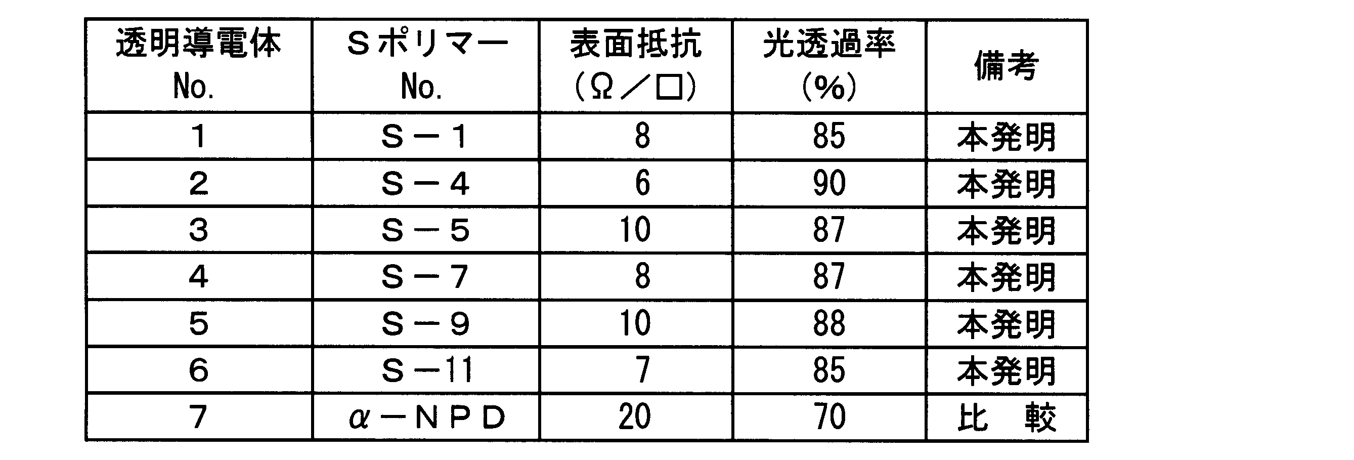
表2より、本発明の試料No.1~6は、比較の試料No.7に比べて表面抵抗が低く、かつ光透過率の高いことが分かる。
<実施例2>
《透明導電体No.11の作製》
(下引き済みPETフィルム透明支持体)
100μmの二軸延伸PET透明支持体の両面に12W・min/m2のコロナ放電処理を施し、それぞれの面に下引き塗布液B-1を乾燥層厚0.1μmになるように塗布し、さらに、それぞれの面のB-1乾燥膜上に12W・min/m2のコロナ放電処理を施し、下引き塗布液B-2を乾燥層厚0.06μmになるように塗布した。その後、120℃で1.5分の熱処理を実施し、下引き済みPETフィルム支持体を得た。
《透明導電体No.11の作製》
(下引き済みPETフィルム透明支持体)
100μmの二軸延伸PET透明支持体の両面に12W・min/m2のコロナ放電処理を施し、それぞれの面に下引き塗布液B-1を乾燥層厚0.1μmになるように塗布し、さらに、それぞれの面のB-1乾燥膜上に12W・min/m2のコロナ放電処理を施し、下引き塗布液B-2を乾燥層厚0.06μmになるように塗布した。その後、120℃で1.5分の熱処理を実施し、下引き済みPETフィルム支持体を得た。
〈下引き塗布液B-1〉
スチレン20質量部、グリシジルメタクリレート40質量部、ブチルアクリレート40質量部の共重合体ラテックス液(固形分質量30%) 50g
化合物(UL-1) 0.2g
水で仕上げる 1000ml
〈下引き塗布液B-2〉
ゼラチン(重量平均分子量:100000) 10g
化合物(UL-1) 0.2g
化合物(UL-2) 0.2g
シリカ粒子(平均粒径3μm) 0.1g
硬膜剤(UL-3) 1g
水で仕上げる 1000ml

スチレン20質量部、グリシジルメタクリレート40質量部、ブチルアクリレート40質量部の共重合体ラテックス液(固形分質量30%) 50g
化合物(UL-1) 0.2g
水で仕上げる 1000ml
〈下引き塗布液B-2〉
ゼラチン(重量平均分子量:100000) 10g
化合物(UL-1) 0.2g
化合物(UL-2) 0.2g
シリカ粒子(平均粒径3μm) 0.1g
硬膜剤(UL-3) 1g
水で仕上げる 1000ml
(下地層の形成:塗布法)
上記透明支持体の上に、表1に記載の重量平均分子量を有する本発明に係るSポリマー(例示化合物S-2)を、実施例1と同様にして塗布し、100nmの下地層を形成した。
上記透明支持体の上に、表1に記載の重量平均分子量を有する本発明に係るSポリマー(例示化合物S-2)を、実施例1と同様にして塗布し、100nmの下地層を形成した。
(透明導電層の形成:塗布法)
銀鏡めっき液は、次のようにして調製した。脱イオン水10000gに硝酸銀20gを溶解した硝酸銀溶液と、別に、脱イオン水10000gに28%アンモニア水溶液100g、モノエタノールアミン5gを溶解してアンモニア溶液を調液した。使用前に、これらの硝酸銀溶液とアンモニア溶液を1対1で混合してアンモニア性硝酸銀溶液とした。次に、脱イオン水10000gに硫酸ヒドラジン10g、モノエタノールアミン5g及び水酸化ナトリウム10gを溶解して還元剤溶液を調液した。
銀鏡めっき液は、次のようにして調製した。脱イオン水10000gに硝酸銀20gを溶解した硝酸銀溶液と、別に、脱イオン水10000gに28%アンモニア水溶液100g、モノエタノールアミン5gを溶解してアンモニア溶液を調液した。使用前に、これらの硝酸銀溶液とアンモニア溶液を1対1で混合してアンモニア性硝酸銀溶液とした。次に、脱イオン水10000gに硫酸ヒドラジン10g、モノエタノールアミン5g及び水酸化ナトリウム10gを溶解して還元剤溶液を調液した。
このようにして得られたアンモニア性硝酸銀溶液と還元剤溶液を、双頭スプレーガンを使用して乾燥後の層厚が10nmとなるように同時に吹き付けて、銀からなる透明導電層を形成させ、脱イオン水にて洗浄した後、70℃30分間乾燥機中で乾燥させて透明導電体No.11を作製した。
《透明導電体No.12~16の作製》
透明導電体No.11の作製において、Sポリマー(例示化合物S-2)を表3に記載したように代え、そのほかは透明導電体No.11の作製と同様にして透明導電体No.12~16を作製した。表1に、用いた各Sポリマーの重量平均分子量を記載した。
透明導電体No.11の作製において、Sポリマー(例示化合物S-2)を表3に記載したように代え、そのほかは透明導電体No.11の作製と同様にして透明導電体No.12~16を作製した。表1に、用いた各Sポリマーの重量平均分子量を記載した。
《透明導電体No.17の作製》
比較の透明導電体として、透明導電体No.11の作製において、Sポリマー(例示化合物S-2)の代わりに、下地層として特許文献3に記載のα-NPDを40nmの厚さで設けた。このときの蒸着チャンバ内の真空度は10-5Pa台で、製膜レートは3Å/sとした。その他は透明導電体No.11の作製と同様にして透明導電体No.17を作製した。
比較の透明導電体として、透明導電体No.11の作製において、Sポリマー(例示化合物S-2)の代わりに、下地層として特許文献3に記載のα-NPDを40nmの厚さで設けた。このときの蒸着チャンバ内の真空度は10-5Pa台で、製膜レートは3Å/sとした。その他は透明導電体No.11の作製と同様にして透明導電体No.17を作製した。
比較として、透明導電体No.11の作製に際し、下地層を設けずに銀からなる導電層を形成したが10nmの厚さの銀の量では、電子顕微鏡観察では均一な膜はできず、30nmで均一な膜となった。しかしながら、反射が強く透明性はほとんどなかった。
《透明導電体の評価》
透明導電体No.11~17の各々について、表面抵抗と透明性を実施例1と同様にして評価した。結果を以下に示す。
透明導電体No.11~17の各々について、表面抵抗と透明性を実施例1と同様にして評価した。結果を以下に示す。
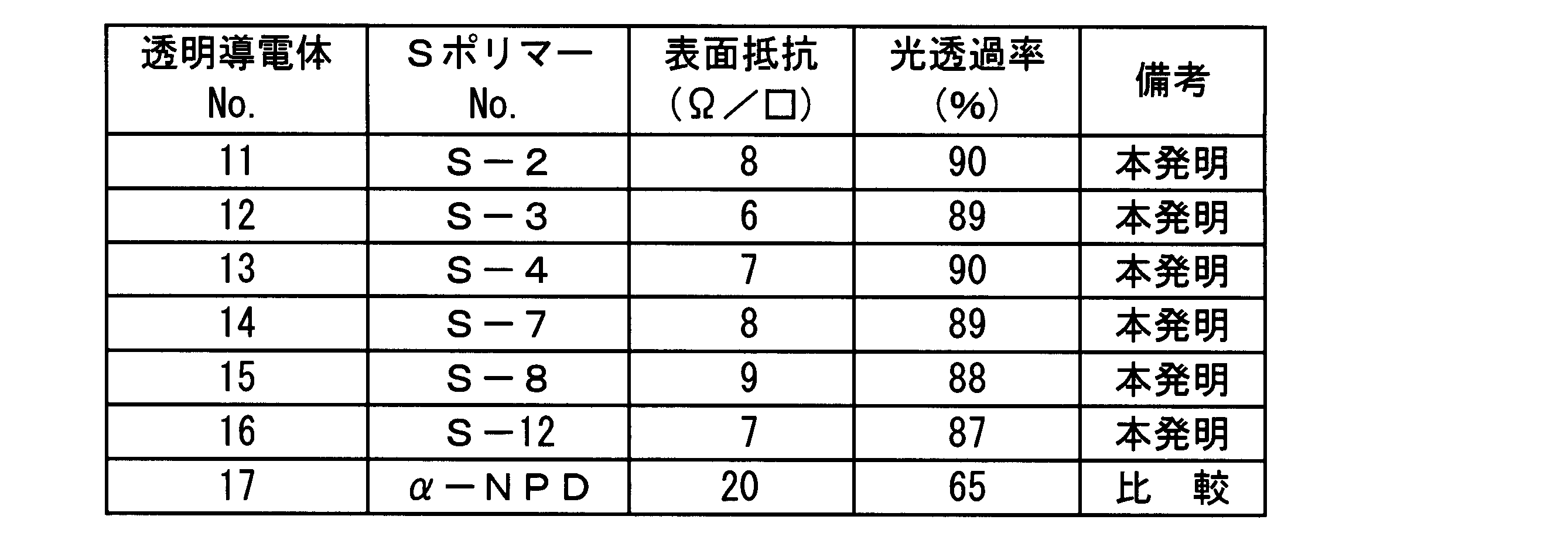
表3より、本発明の試料No.11~16は、比較の試料No.17に比べて表面抵抗が低く、かつ光透過率の高いことが分かる。
本発明の透明導電体は、液晶、プラズマ、有機エレクトロルミネッセンス、フィールドエミッションなど各種方式のディスプレイをはじめ、タッチパネルや携帯電話、電子ペーパー、各種太陽電池、各種エレクトロルミネッセンス調光素子など様々なオプトエレクトロニクスデバイスの基板等に好ましく用いることができる。
1 透明導電体
2 透明支持体
3 下地層
4 透明導電層
2 透明支持体
3 下地層
4 透明導電層
Claims (4)
- 透明支持体上に、硫黄原子を有し重量平均分子量が1000~1000000の範囲内であるポリマーを含有する下地層と、該下地層に隣接する銀又は銀の合金を含有する透明導電層とを有することを特徴とする透明導電体。
- 前記ポリマーが、芳香族環を有することを特徴とする請求項1に記載の透明導電体。
- 前記透明導電層の層厚が、1~20nmの範囲内にあることを特徴とする請求項1又は請求項2に記載の透明導電体。
- 波長550nmでの光透過率が、80%以上であることを特徴とする請求項1から請求項3までのいずれか一項に記載の透明導電体。
Priority Applications (1)
| Application Number | Priority Date | Filing Date | Title |
|---|---|---|---|
| JP2015506753A JPWO2014148407A1 (ja) | 2013-03-21 | 2014-03-17 | 透明導電体 |
Applications Claiming Priority (2)
| Application Number | Priority Date | Filing Date | Title |
|---|---|---|---|
| JP2013-057522 | 2013-03-21 | ||
| JP2013057522 | 2013-03-21 |
Publications (1)
| Publication Number | Publication Date |
|---|---|
| WO2014148407A1 true WO2014148407A1 (ja) | 2014-09-25 |
Family
ID=51580086
Family Applications (1)
| Application Number | Title | Priority Date | Filing Date |
|---|---|---|---|
| PCT/JP2014/057042 Ceased WO2014148407A1 (ja) | 2013-03-21 | 2014-03-17 | 透明導電体 |
Country Status (2)
| Country | Link |
|---|---|
| JP (1) | JPWO2014148407A1 (ja) |
| WO (1) | WO2014148407A1 (ja) |
Cited By (2)
| Publication number | Priority date | Publication date | Assignee | Title |
|---|---|---|---|---|
| WO2018074217A1 (ja) * | 2016-10-17 | 2018-04-26 | アルプス電気株式会社 | 複合成形部材および複合成形部材の製造方法、ならびに電子・電気部品および電子・電気部品の製造方法 |
| JP2019073588A (ja) * | 2017-10-13 | 2019-05-16 | Jsr株式会社 | 硬化性組成物 |
Citations (5)
| Publication number | Priority date | Publication date | Assignee | Title |
|---|---|---|---|---|
| JP2005019056A (ja) * | 2003-06-24 | 2005-01-20 | Toray Ind Inc | 複合透明導電性基材とそれを用いたディスプレイ |
| JP2009170408A (ja) * | 2007-12-20 | 2009-07-30 | Shin Etsu Polymer Co Ltd | 導電性シートおよびその製造方法、ならびに入力デバイス |
| JP2012206326A (ja) * | 2011-03-29 | 2012-10-25 | Mitsubishi Paper Mills Ltd | 銀メッキ塗装体 |
| JP5061262B1 (ja) * | 2012-03-09 | 2012-10-31 | 株式会社フジクラ | 導電性高分子組成物および導電体 |
| WO2013161785A1 (ja) * | 2012-04-26 | 2013-10-31 | コニカミノルタ株式会社 | 透明ガスバリアーフィルム及び電子デバイス |
-
2014
- 2014-03-17 WO PCT/JP2014/057042 patent/WO2014148407A1/ja not_active Ceased
- 2014-03-17 JP JP2015506753A patent/JPWO2014148407A1/ja active Pending
Patent Citations (5)
| Publication number | Priority date | Publication date | Assignee | Title |
|---|---|---|---|---|
| JP2005019056A (ja) * | 2003-06-24 | 2005-01-20 | Toray Ind Inc | 複合透明導電性基材とそれを用いたディスプレイ |
| JP2009170408A (ja) * | 2007-12-20 | 2009-07-30 | Shin Etsu Polymer Co Ltd | 導電性シートおよびその製造方法、ならびに入力デバイス |
| JP2012206326A (ja) * | 2011-03-29 | 2012-10-25 | Mitsubishi Paper Mills Ltd | 銀メッキ塗装体 |
| JP5061262B1 (ja) * | 2012-03-09 | 2012-10-31 | 株式会社フジクラ | 導電性高分子組成物および導電体 |
| WO2013161785A1 (ja) * | 2012-04-26 | 2013-10-31 | コニカミノルタ株式会社 | 透明ガスバリアーフィルム及び電子デバイス |
Cited By (2)
| Publication number | Priority date | Publication date | Assignee | Title |
|---|---|---|---|---|
| WO2018074217A1 (ja) * | 2016-10-17 | 2018-04-26 | アルプス電気株式会社 | 複合成形部材および複合成形部材の製造方法、ならびに電子・電気部品および電子・電気部品の製造方法 |
| JP2019073588A (ja) * | 2017-10-13 | 2019-05-16 | Jsr株式会社 | 硬化性組成物 |
Also Published As
| Publication number | Publication date |
|---|---|
| JPWO2014148407A1 (ja) | 2017-02-16 |
Similar Documents
| Publication | Publication Date | Title |
|---|---|---|
| CN111621201B (zh) | 用于形成具有稠合网络的透明导电膜的金属纳米线油墨 | |
| CN104040644B (zh) | 透明导电性膜及图像显示装置 | |
| TWI485721B (zh) | Transparent conductive film and touch panel | |
| US10437112B2 (en) | Transparent electrode, touch sensor and image display device including the same | |
| TW201119866A (en) | Transparent conductive film, method for production thereof and touch panel therewith | |
| CN107533880B (zh) | 透明导电性薄膜 | |
| JP2012003900A (ja) | 導電膜及びその製造方法、並びにタッチパネル及び集積型太陽電池 | |
| CN106959484A (zh) | 偏振片、偏光板和图像显示装置 | |
| JP2010231171A (ja) | 光学物品およびその製造方法 | |
| TWI706300B (zh) | 薄膜觸控感測器 | |
| CN101133463A (zh) | 结晶性透明导电性薄膜、其制造方法、透明导电性薄膜及触摸面板 | |
| CN107004463A (zh) | 透明导电性薄膜以及使用其的触摸传感器 | |
| CN103875042A (zh) | 透明导电性薄膜 | |
| JPH02129808A (ja) | 透明導電性積層体 | |
| WO2014148407A1 (ja) | 透明導電体 | |
| JP6425598B2 (ja) | 透明導電性フィルム及びタッチパネル | |
| CN110088714B (zh) | 带载体薄膜的透明导电性薄膜及使用其的触摸面板 | |
| TWI633563B (zh) | Transparent conductive film with carrier film and touch panel using the same | |
| KR20170112310A (ko) | 투명 전극 구조체 및 이의 제조방법 | |
| WO2022071422A1 (ja) | センサー、物品、センサーの製造方法、および導電体 | |
| JP2018507507A (ja) | 金属ナノワイヤーを含む透明導電体、及びこれを形成する方法 | |
| JP2014210372A (ja) | ハードコートフィルム及びそれを備えた透明導電性フィルム、タッチパネル、並びにハードコート塗液 | |
| WO2015045965A1 (ja) | タッチパネル用積層体、タッチパネル | |
| JP2000243146A (ja) | 透明導電性フィルムおよびこれを用いたタッチパネル | |
| CN102343698A (zh) | 一种硬质薄膜及其制备方法 |
Legal Events
| Date | Code | Title | Description |
|---|---|---|---|
| 121 | Ep: the epo has been informed by wipo that ep was designated in this application |
Ref document number: 14769807 Country of ref document: EP Kind code of ref document: A1 |
|
| ENP | Entry into the national phase |
Ref document number: 2015506753 Country of ref document: JP Kind code of ref document: A |
|
| NENP | Non-entry into the national phase |
Ref country code: DE |
|
| 122 | Ep: pct application non-entry in european phase |
Ref document number: 14769807 Country of ref document: EP Kind code of ref document: A1 |