WO2014142140A1 - 発光管アレイ - Google Patents
発光管アレイ Download PDFInfo
- Publication number
- WO2014142140A1 WO2014142140A1 PCT/JP2014/056399 JP2014056399W WO2014142140A1 WO 2014142140 A1 WO2014142140 A1 WO 2014142140A1 JP 2014056399 W JP2014056399 W JP 2014056399W WO 2014142140 A1 WO2014142140 A1 WO 2014142140A1
- Authority
- WO
- WIPO (PCT)
- Prior art keywords
- arc tube
- arc
- electrode
- flat surface
- electrode group
- Prior art date
- Legal status (The legal status is an assumption and is not a legal conclusion. Google has not performed a legal analysis and makes no representation as to the accuracy of the status listed.)
- Ceased
Links
Images



Classifications
-
- H—ELECTRICITY
- H01—ELECTRIC ELEMENTS
- H01J—ELECTRIC DISCHARGE TUBES OR DISCHARGE LAMPS
- H01J11/00—Gas-filled discharge tubes with alternating current induction of the discharge, e.g. alternating current plasma display panels [AC-PDP]; Gas-filled discharge tubes without any main electrode inside the vessel; Gas-filled discharge tubes with at least one main electrode outside the vessel
- H01J11/20—Constructional details
- H01J11/22—Electrodes, e.g. special shape, material or configuration
- H01J11/24—Sustain electrodes or scan electrodes
-
- H—ELECTRICITY
- H01—ELECTRIC ELEMENTS
- H01J—ELECTRIC DISCHARGE TUBES OR DISCHARGE LAMPS
- H01J11/00—Gas-filled discharge tubes with alternating current induction of the discharge, e.g. alternating current plasma display panels [AC-PDP]; Gas-filled discharge tubes without any main electrode inside the vessel; Gas-filled discharge tubes with at least one main electrode outside the vessel
- H01J11/10—AC-PDPs with at least one main electrode being out of contact with the plasma
- H01J11/18—AC-PDPs with at least one main electrode being out of contact with the plasma containing a plurality of independent closed structures for containing the gas, e.g. plasma tube array [PTA] display panels
-
- H—ELECTRICITY
- H01—ELECTRIC ELEMENTS
- H01J—ELECTRIC DISCHARGE TUBES OR DISCHARGE LAMPS
- H01J11/00—Gas-filled discharge tubes with alternating current induction of the discharge, e.g. alternating current plasma display panels [AC-PDP]; Gas-filled discharge tubes without any main electrode inside the vessel; Gas-filled discharge tubes with at least one main electrode outside the vessel
- H01J11/20—Constructional details
- H01J11/22—Electrodes, e.g. special shape, material or configuration
- H01J11/26—Address electrodes
Definitions
- the present invention relates to an improvement of an arc tube array configured by arranging a plurality of arc tubes (plasma tubes) in parallel, and more particularly to an arc tube array that enables high definition without causing an increase in driving voltage.
- An arc tube array configured by juxtaposing a plurality of arc tubes filled with discharge gas inside has been developed as a film display device or a planar light source.
- the arc tube array is, for example, a film-shaped light emitting device in which 1000 to 1 or more arc tubes (plasma tubes) having a tube diameter of 0.5 to 1 mm are juxtaposed in an array (arc tube array).
- arc tube array Configured as Further, for example, a 1 m square arc tube array can be used as a display submodule, and a plurality of display submodules can be connected to arbitrarily expand the screen size to constitute an ultra-large arc tube array type display device.
- the arc tube array uses thin glass tubes as a manufacturing unit, it does not require a large-scale facility for handling large glass substrates that are necessary when manufacturing large display panels such as LCDs and PDPs, and is also transported. Thus, installation and the like are facilitated, and an ultra-large display device can be provided at low cost.
- Patent Document 1 discloses a configuration of an arc tube in which the cross-sectional shape is a horizontally long flat shape, and the ratio of the major axis to the minor axis is in the range of 10: 7 to 5: 1.
- Patent Document 2 discloses a method for producing a flat elliptical glass capillary.
- the pixel size is determined by the major axis of the cross section of the arc tube. That is, in the case of configuring a color display device, one pixel is composed of three arc tubes each corresponding to three colors of RGB, so if the arc tube has a tube diameter of 1 mm, the size of one pixel is 3 mm.
- the arc tube having the configuration disclosed in Patent Document 1 it has been difficult to construct a high-definition color display device having a pixel size of 3 mm or less.
- the minor axis becomes excessively short, and the surface area of the phosphor layer formed on the inner wall of the arc tube decreases with a decrease in the tube volume.
- the surface area of the phosphor layer formed on the inner wall of the arc tube decreases with a decrease in the tube volume.
- the present invention has been made in view of such circumstances, and is intended to improve resolution by increasing the arrangement density of arc tubes in an arc tube array configured by juxtaposing a plurality of arc tubes. Specifically, it is an object of the present invention to provide an arc tube array capable of ensuring sufficient luminance without causing an increase in driving voltage even when the definition is increased.
- an arc tube array according to the first invention includes a plurality of arc tubes arranged side by side, a first electrode group extending in a direction crossing the arc tube, and the length of each arc tube.
- a second electrode group provided along a direction, the arc tube has a substantially flat quadrangular cross section, and the first electrode group is provided in contact with one flat surface of each arc tube The second electrode group is provided in contact with a side flat surface adjacent to the one flat surface of each arc tube.
- the arc tube array according to a second aspect of the present invention is the arc tube array according to the first aspect, wherein the first electrode group is in contact with one flat surface on the short diameter side of each arc tube as a discharge electrode pair, and the second electrode group is an address.
- the electrode is in contact with one flat surface on the long diameter side.
- An arc tube array according to a third invention is the arc tube array according to the first invention, wherein the first electrode group is in contact with one flat surface on the short diameter side of each arc tube as an address electrode, and the second electrode group is discharged.
- the electrode pair is in contact with at least one flat surface on the major axis side of each arc tube.
- the arc tube array according to a fourth invention is characterized in that, in the third invention, the second electrode group is shared by two adjacent arc tubes.
- the arc tube array according to a fifth invention is characterized in that, in the third invention, the second electrode group is provided as a discharge electrode pair on a flat surface on both opposite sides on the major axis side of each arc tube. To do.
- the arc tube array according to a sixth aspect of the present invention is the arc tube array according to any one of the first to fifth aspects, wherein the arc tube has a cross-sectional shape orthogonal to the longitudinal direction, the first and It is characterized in that it is a pseudo-octagon shape of a vertically long flat shape having a second flat surface, third and fourth flat surfaces facing each other on the long diameter side, and four curved surfaces connecting between the four flat surfaces. .
- the arc tube constituting the arc tube array of the present invention has a substantially flat quadrilateral cross section, and includes an address electrode and a discharge electrode pair on two adjacent flat surfaces, respectively.
- An address discharge is generated at the corner. Accordingly, even when a high-definition arc tube array is formed by vertically arranging the long diameter side, the address discharge gap can be shortened and the address discharge voltage can be kept low without reducing the volume of the gas discharge space. Therefore, the present invention is extremely useful for practical application of an arc tube array used as a planar light source or a large-screen high-definition display device.
- FIG. 1 is a perspective view schematically showing a configuration of a conventional arc tube array.
- the conventional arc tube array 3 is configured by juxtaposing a plurality of arc tubes 31, 31,.
- the cross sections of the arc tubes 31, 31,... Are shown in a circular shape for convenience, but the arc tubes 31, 31,.
- the diameter of the glass capillary used as the tubular body is not particularly limited, the minor axis is preferably 1 mm or less and the major axis is preferably about 1 to 3 mm.
- a discharge gas such as neon or xenon is sealed in the arc tube 31, 31,.
- a display electrode sheet 35 having display electrode pairs 34, 34,... Formed in a direction intersecting with the longitudinal direction of the arc tubes 31, 31,.
- the display electrode sheet 35 is a flexible sheet, and is composed of, for example, a polycarbonate film, a PET (polyethylene terephthalate) film, or the like.
- the plurality of display electrode pairs 34, 34,... are formed in a stripe shape on the front side of the arc tube array 3 in a direction that intersects the longitudinal direction of the arc tubes 31, 31,.
- the display electrode pairs 34, 34,... are not particularly limited as long as they can generate a display discharge in the arc tubes 31, 31,... Between the adjacent display electrodes 34, 34. Absent.
- the display electrode 34 can be formed using various materials known in the art. Examples of the material used for the display electrode 34 include transparent conductive materials such as ITO (tin oxide doped indium oxide) and SnO 2 , and Ag, Au, and Al formed with a translucent pattern such as a mesh or a ladder. , Cu, Cr, and other conductive materials.
- the cross-sectional shape perpendicular to the longitudinal direction of each arc tube 31 constituting the arc tube array 3 is made into a vertically long flat quadrilateral shape with the major axis side being vertical, and the arrangement pitch is narrowed.
- the address electrode 32 and the display electrode 34 are provided to face each other on the tube wall portion on the short diameter side.
- the address discharge gap has a length corresponding to the major axis dimension of the arc tube (flat tube) 31, and thus it is difficult to avoid an increase in the address discharge voltage.
- FIG. 2 is an enlarged perspective view partially showing the configuration of the arc tube array according to Embodiment 1 of the present invention.
- a red (R) phosphor layer 36R for each arc tube 31, a red (R) phosphor layer 36R, a green (G) phosphor layer 36G, and a blue (B) layer.
- a phosphor layer 36 ⁇ / b> B is formed on the inner wall of the arc tube 31.
- the phosphor layer 36R is made of a phosphor material such as (Y, Gd) BO 3 : Eu 3+ that emits red light when irradiated with ultraviolet rays generated by gas discharge.
- a phosphor material such as Zn 2 SiO 4 : Mn that emits green light is used
- BaMgAl 12 O 17 Eu that emits blue light.
- a phosphor material such as 2+ is used.
- the shape of the cross section orthogonal to the longitudinal direction of the arc tube 31 is a vertically long quadrilateral shape in which the major axis side is longitudinal, and the address electrode 32 is provided on the side surface of each arc tube 31. It has a feature in that. 3 is a cross-sectional view taken along a plane orthogonal to the longitudinal direction of the arc tubes 31, 31,... Partially showing the configuration of the arc tube array according to Embodiment 1 of the present invention.
- the arc tube 31 of the arc tube array according to the first embodiment has a cross-sectional shape orthogonal to the longitudinal direction, which has a minor axis a and a major axis b, and the major axis b side is longitudinal. It has a vertically long flat quadrilateral shape. In a strict sense, it is impossible to manufacture a glass tube having a flat quadrilateral cross section.
- the shape of the cross section perpendicular to the longitudinal direction of the arc tube 31 is an upper and lower flat surface on the minor axis a side ( (First flat surface and second flat surface) 41, 42 and left and right flat surfaces (third flat surface and fourth flat surface) 43 on the long diameter b side, and four corners connecting the four flat surfaces
- a pseudo octagon shape having a portion (curved surface) 44 is obtained.
- a phosphor layer 36 is formed inside a first flat surface (lower flat surface) 41, which is the opposite side of the display surface, and is in contact with a second flat surface (upper flat surface) 42 facing the display electrode sheet 35.
- a supported display electrode pair (discharge electrode pair) 34 is provided.
- the address electrode 32 is provided in contact with either the third flat surface or the fourth flat surface (side flat surface) 43 adjacent in the arrangement direction.
- the address electrode 32 has a mesh pattern electrode configuration supported by a tape-like PET film (address electrode sheet) 33, and is formed on the left flat surface (third flat surface) 43 of each arc tube 31. It is attached with an adhesive that passes through the electrode mesh.
- the tape-shaped PET film 33 has a non-selective shielding function with respect to the arc tube 31 adjacent on the left side.
- the address electrode 32 may be formed by directly printing a conductor paste (Ag paste) on the third flat surface 43 of each arc tube 31.
- the printed silver electrode film is protected, and the electrode film surface is covered with an acrylic resin or the like so that the electric field penetration strength with respect to the adjacent arc tube 31 is lowered.
- an electric field shield layer may be provided on the fourth flat surface 43 facing the address electrode 32, or a space may be provided between the tube walls of the adjacent arc tubes 31 and 31.
- the thickness of the tube wall of the other flat surface opposite to the thickness of the tube wall of the one flat surface forming the address electrode 32 is made thick so that the adjacent arc tubes 31 and 31 It is also possible to effectively apply an address electric field to one.
- the minor axis (width) a of the cross section of the arc tube 31 defining the pixel width is preferably 1 mm or less from the viewpoint of high definition.
- the major axis (height) b is shorter than the minor axis a, the amount of the phosphor is reduced, and it is difficult to ensure sufficient luminance.
- the major axis (height) b is longer than three times the minor axis a, the distance from the display electrode pair 34 to the phosphor layer 36 becomes relatively long, and the attenuation of ultraviolet rays due to discharge increases. It becomes difficult to ensure sufficient luminance. Therefore, the relationship between the minor axis a and the major axis b is preferably in the range of 3a ⁇ b> a.
- the shape of the cross section perpendicular to the longitudinal direction of the arc tube 31 is a vertically long flat quadrilateral shape, so that when the arc tubes 31 are juxtaposed, the arc tubes 31 are not easily toppled and positioning is easy.
- the address electrode 34 is directly formed on either the third flat surface or the fourth flat surface 43 of each arc tube 31, the flat surfaces to be the electrode forming surfaces of the plural arc tubes 31 are aligned.
- the conductor paste can be easily formed simultaneously by printing the conductor paste through a predetermined printing mask.
- a discharge auxiliary film 53 including a surface layer 51 made of a metal oxide and a magnesium oxide crystal fine particle group 52 partially exposed from the surface layer 51 is provided.
- the surface layer of the metal oxide is formed as a crystal film containing at least one of MgO, CaO, BaO, SrO and the like, and a part of the magnesium oxide crystal particle group 52 is exposed from the surface layer 51.
- the oxide of the Group 2 element of the periodic table has a large secondary electron emission coefficient and has an effect of reducing the discharge voltage by facing the gas discharge space.
- magnesium oxide is the most suitable material for the discharge surface. Due to the presence of the discharge auxiliary film 53 composed of the magnesium oxide surface layer 51 and the magnesium oxide crystal particle group 52, the inside of the arc tube 31 is easily discharged.
- FIG. 4 is an exemplary view showing a manufacturing process of the arc tube 31 of the arc tube array according to Embodiment 1 of the present invention.
- both ends of a borosilicate glass mother tube 45 having a cross-sectional diameter of 10 mm, a tube thickness of 1.0 mm, and a length of 500 mm are heated and melted and sealed, and air is sealed inside.
- the airtight glass mother tube 45 is placed in the forming jig 46 (see the left figure in FIG. 4A).
- the forming jig 46 has a rectangular cross section of 8.6 mm ⁇ 11.8 mm, for example, and has a length that allows the glass mother tube 45 to be accommodated.
- ceramics quartz, aluminum nitride, boron nitride, It is preferable to use silicon nitride, silicon carbide, or the like.
- the forming jig 46 on which the glass mother tube 45 is placed is left in a heating furnace (not shown), and the temperature is increased to 640 ° C. Then, the air in the glass mother tube 45 expands to increase the internal pressure and the glass mother tube 45 itself is softened. Therefore, the glass mother tube 45 has a shape (a cross section of the inner surface of the forming jig 46). It is deformed into a vertically long flat quadrilateral shape.
- a glass tube preform 47 whose cross section is a vertically long and flat quadrilateral shape is completed (see the right figure in FIG. 4A). At the time of cooling, the glass tube 45 is cooled before the air inside the glass tube 45, so that the glass tube preform 47 can maintain its shape.
- the glass mother tube 45 may have a diameter larger than the height of the inner surface of the forming jig 46 and not fit in the forming jig 46.
- the molding jig 46 on which the glass mother tube 45 is placed is left in the heating furnace with the upper lid 46a of the molding jig 46 away from the other parts of the molding jig 46, and above the upper lid 46a.
- a constant pressure 100 is applied to soften the glass mother tube 45 (see the left figure in FIG. 4B).
- the glass mother tube 45 is deformed into a shape along the shape of the inner surface of the forming jig 46 (the cross section is a vertically long flat quadrilateral shape), and the deformed glass mother tube 45 is placed in the forming jig 46.
- the glass tube preform 47 whose cross section is a vertically long flat quadrilateral is completed (see the right figure in FIG. 4B).
- a glass tube preform 47 whose cross section is a vertically long flat quadrilateral shape may be similarly formed (FIG. 4C). reference).
- the glass tube preform 47 thus formed is redrawn and drawn to a predetermined dimension in the next step, thereby producing a glass tube that serves as an envelope of the arc tube 31 having a similar cross section.
- the produced glass tube is cut into a predetermined length, and the arc tube 31 can be produced through processes such as formation of a discharge protective film, formation of a phosphor layer, gas sealing and sealing, and the like.
- the arc tube 31 has a cross-sectional shape perpendicular to the longitudinal direction, which is a vertically long quadrilateral shape with the long diameter b side being vertical, and the tube wall on the long diameter b side is The arc tube arrays are arranged side by side so as to be adjacent to each other.
- the shape of the cross section perpendicular to the longitudinal direction of the arc tube 31 is a vertically long flat quadrilateral shape (strictly, a pseudo-octagon shape)
- a stable discharge with a sufficient contact area between the arc tube 31 and the display electrode 34 is ensured.
- the characteristics can be obtained and the volume of the arc tube 31 is not reduced even though the tube diameter dimension on the short axis a side is shortened, the surface area of the phosphor layer 36 formed on the inner wall can be substantially reduced. Absent. Therefore, it is possible to provide a high-definition arc tube array type color display device having a pixel size of 3 mm or less while ensuring a certain luminance.
- the second flat surface (upper flat surface) 42 in contact with the display electrode 34 and the third flat surface (side flat surface) 43 in contact with the address electrode 32 are provided.
- An address discharge (selective discharge) is generated at the corner (curved surface) 44a as indicated by an arrow 45. Since the distance of the discharge gap between the electrodes is shortened, the reset discharge voltage and address discharge voltage are not increased, and the arc tube array is equal to or less than the arc tube array in which the transverse cross-sections are arranged in parallel. It can be driven by voltage.
- the counter discharge voltage across the major axis of 1 mm is 120 to 150 V, but the corner discharge type diagonal counter discharge voltage according to the present invention is greatly reduced to 50 to 70 V in the arc tube 31 of the same size.
- the arc tube 31 may be configured by inserting a phosphor support member (boat) in which the phosphor layer 36 is formed into a glass tube.
- FIG. 5 shows that the phosphor layer 36 is provided by inserting a phosphor support member having a bowl-shaped (U-shaped) cross section into each arc tube 31 of the arc tube array according to Embodiment 1 of the present invention. It is sectional drawing in the surface orthogonal to the longitudinal direction in the case.
- the address voltage is greatly increased by the insertion of the phosphor support member.
- the phosphor support member hardly affects the address discharge voltage.
- the phosphor support member 50 has a bowl-shaped (U-shaped) cross section with the first flat surface 41 on the short diameter side as the bottom, and the phosphor layer 36 includes the phosphor support member. 50 is formed on the inner surface.
- the length b2 of the phosphor support member 50 in the major axis direction is shorter than the major axis b1 of the arc tube 31, but in order to ensure sufficient luminance, it is longer than half of the major axis b1, and preferably longer than two thirds. Is preferred.
- the arc tube 31 has a long diameter side of each arc tube 31 such that the display electrodes 34, 34,... Are shared by two arc tubes adjacent in the arrangement direction. Is different from the first embodiment in that the address electrodes 32, 32,... Are provided in contact with the lower flat surface on the short diameter side. To do.
- the display electrodes 34 shared by two adjacent arc tubes 31 alternately function as an X electrode and a Y electrode.
- FIG. 6 is a cross-sectional view taken along a plane orthogonal to the longitudinal direction of the arc tubes 31, 31,... Partially showing the configuration of the arc tube array according to Embodiment 2 of the present invention.
- the same reference numerals are given to the same parts as those in the first embodiment.
- the arc tube 31 of the arc tube array according to Embodiment 2 also has a vertically long quadrilateral shape in which the cross section perpendicular to the longitudinal direction is vertical on the long diameter b side.
- the discharge electrodes 34a, 34b are arranged along the longitudinal direction on one flat surface (third flat surface or fourth flat surface) 43 on the long diameter b side of each arc tube 31 having a pseudo octagonal cross section. Are formed, and are shared by two arc tubes 31 and 31 adjacent to each other back to back. Since the discharge electrode 34a and the discharge electrode 34b alternately function as an X electrode and a Y electrode, by alternately applying a discharge voltage pulse between the two electrodes, a counter discharge gap having a short diameter dimension is sandwiched horizontally. Sustain discharge occurs.
- the discharge electrode 34a functioning as the X electrode is divided into two groups of the X electrode group X1 and the X electrode group X2 that are alternately adjacent to each other, and the discharge voltage pulse is applied in the order of Y ⁇ X1 ⁇ Y ⁇ X2.
- the light emitting tube group (for example, X electrode group X1) and the even numbered light emitting tube group (for example, X electrode group X2) can emit light alternately.
- the discharge electrodes 34a and 34b shared between the adjacent arc tubes 31 and 31 can be configured by contacting the conductive films printed on both sides of each arc tube 31 in a back-to-back manner.
- the adjacent conductive films may be bonded with a conductive adhesive or a conductive tape.
- the plurality of address electrodes 32, 32,... are formed on the address electrode sheet 33 in a direction crossing the arc tube 31, and are provided in contact with the first flat surface 41 of each arc tube 31. ing. That is, the address electrode 32 is provided in contact with the flat surface of the arc tube 31 on the side provided with the phosphor layer 36. Therefore, the address discharge is performed as shown by an arrow 45 at a corner portion (curved surface) 44b between the address electrode 32 and the discharge electrode 34b functioning as a Y electrode between every two adjacent light emitting tubes 31. appear.
- the discharge electrode 34a functioning as the X electrode is divided into two groups of the X electrode group X1 and the X electrode group X2 that are alternately adjacent, and a voltage having a polarity that cancels the address electric field is selectively applied.
- the discharge electrodes 34b functioning as the Y electrodes share the two arc tubes 31 and 31 that share the scan electrode, and can alternately perform divided addressing to perform so-called interlace driving.
- the address electrode sheet 33 on which the address electrodes 32 extend is provided on the back side of the array array surface, and the front side does not block light emission.
- Light from the body layer 36 can be efficiently extracted from the front side as indicated by a dotted arrow.
- a film-like arc tube array as an ultraviolet light source can be obtained. .
- a pair of X electrodes 34a and Y electrodes 34b are arranged for each arc tube 31 as display electrodes 34, 34,. , 31 is different from the second embodiment in that an insulating layer is provided between them.
- FIG. 7 is a cross-sectional view taken along a plane perpendicular to the longitudinal direction of arc tubes 31, 31,... Partially showing the configuration of the arc tube array according to Embodiment 3 of the present invention.
- the same reference numerals are given to the parts equivalent to those in the first and second embodiments.
- the arc tube 31 of the arc tube array according to Embodiment 3 also has a vertically long quadrilateral shape in which the cross section perpendicular to the longitudinal direction has a longitudinal axis b sideways.
- the X electrode 34a and the Y electrode 34b are provided on the third flat surface and the fourth flat surface (side flat surface) 43, 43 on the major axis b side of each arc tube 31, respectively. It is provided for each. Further, the plurality of address electrodes 32, 32,... Are formed on the first flat surface 41 of the arc tube 31 in a direction crossing the arc tube 31 on the address electrode sheet 33, as in the second embodiment. It is provided in contact.
- a pair of X electrodes 34a and Y electrodes 34b are arranged for each arc tube 31, and adjacent to each other.
- An intermediate insulating layer 60 is provided between the arc tubes 31 and 31 to prevent a short circuit between the X electrode 34a and the Y electrode 34b.
- the X electrode 34a and the Y electrode 34b in the third embodiment are not directly formed on the side surface of the arc tube 31 as described above, but an electrode assembly in which a strip conductor film is formed on both sides of the strip support is created.
- the arc tube array can be configured by sandwiching the created electrode assembly between the side flat surfaces of the adjacent arc tubes 31 and 31.
- the belt-like conductor film is preferably a mesh pattern.
- the arc tube array in which the long diameter of the arc tube 31 having a vertically long flat quadrilateral cross section is arranged in parallel is mainly described, but address discharge at the corner portion 44 is possible.
- the electrode arrangement of the present invention can achieve stable and reliable driving because the address discharge voltage can be lowered even when the arc tube 31 having a vertically long and flat quadrangular cross section is juxtaposed in the horizontal direction. Useful on.
- the present invention is not limited to the above-described embodiment, and various modifications and replacements are possible.
Landscapes
- Engineering & Computer Science (AREA)
- Physics & Mathematics (AREA)
- Plasma & Fusion (AREA)
- Chemical & Material Sciences (AREA)
- Materials Engineering (AREA)
- Gas-Filled Discharge Tubes (AREA)
Abstract
複数の発光管を並置して構成された発光管アレイにおいて、高精細化した場合であっても駆動電圧の上昇を招くことなく十分な輝度を確保することができる発光管アレイを提供する。 並置して配列された複数の発光管(31)と、発光管(31)を横切る方向に延伸する第1の電極群と、各発光管(31)の長手方向に沿って設けられた第2の電極群とを備え、発光管(31)が略扁平四辺形状の横断面を有し、第1の電極群が各発光管(31)の一の平坦面に接して設けられ、第2の電極群が各発光管(31)の一の平坦面に隣接した側方の平坦面に接して設けられている。アドレス放電は、隣接する平坦面のコーナー部で発生する。
Description
本発明は、複数の発光管(プラズマチューブ)を並置して構成された発光管アレイの改良に関し、さらに詳しくは、駆動電圧の上昇を招くことなく高精細化を可能とした発光管アレイに関する。
内部に放電ガスが封入された複数の発光管を並置して構成された発光管アレイがフィルム状の表示装置又は平面光源として開発されている。発光管アレイは、例えば0.5~1mmの管径を有する1~2mの長さの発光管(プラズマチューブ)を1000本乃至それ以上アレイ状に並置(発光管アレイ)したフィルム状の発光デバイスとして構成される。また、例えば1m平方の発光管アレイを表示サブモジュールとし、複数の表示サブモジュールを接続して画面サイズを任意に拡張して、超大型の発光管アレイ型表示装置を構成することができる。発光管アレイは、細いガラス管を製造単位とするので、LCD、PDPのような大型表示パネルを製造する場合に必要となる大きなガラス基板を取り扱うための大規模な設備が不要となるとともに、運搬、設置等も容易となり、超大型の表示装置を安価に提供することができる。
発光管アレイを構成する発光管の代表的な構成は、特許文献1に開示されている。特許文献1では、横断面の形状が横長扁平形状であり、長径と短径との比が、10:7~5:1の範囲である発光管の構成が開示されている。また、扁平楕円状のガラス細管の製造方法については、特許文献2に開示されている。
上述した従来の発光管アレイを表示装置として用いる場合、発光管の横断面の長径により画素のサイズが決定される。すなわち、カラー表示装置を構成する場合には、RGB3色にそれぞれ対応する3本の発光管で1画素を構成するため、管径が1mmの発光管であれば1画素のサイズは3mmとなる。しかし、特許文献1に開示されている構成の発光管では、画素のサイズが3mm以下といった高精細のカラー表示装置を構成することは困難であるというのが実情であった。すなわち、画素のサイズを小さくするために長径を短くすると、短径が過度に短くなり、管内容積の減少に伴って発光管の内壁に形成される蛍光体層の表面積が小さくなるので、表示装置として十分な輝度を確保することができないという問題点があった。
本発明は斯かる事情に鑑みてなされたものであり、複数の発光管を並置して構成された発光管アレイにおいて発光管の配置密度を高めて解像度の向上を図ろうとするものであり、さらに詳細には、高精細化した場合であっても駆動電圧の上昇を招くことなく十分な輝度を確保することができる発光管アレイを提供することを目的とする。
上記目的を達成するために第1発明に係る発光管アレイは、並置して配列された複数の発光管と、該発光管を横切る方向に延伸する第1の電極群と、各発光管の長手方向に沿って設けられた第2の電極群とを備え、前記発光管が略扁平四辺形状の横断面を有し、前記第1の電極群が各発光管の一の平坦面に接して設けられ、前記第2の電極群が各発光管の前記一の平坦面に隣接した側方の平坦面に接して設けられていることを特徴とする。
また、第2発明に係る発光管アレイは、第1発明において、前記第1の電極群が放電電極対として各発光管の短径側の一の平坦面に接し、第2の電極群がアドレス電極として長径側の一の平坦面に接していることを特徴とする。
また、第3発明に係る発光管アレイは、第1発明において、前記第1の電極群がアドレス電極として各発光管の短径側の一の平坦面に接し、前記第2の電極群が放電電極対として各発光管の長径側の少なくとも一の平坦面に接していることを特徴とする。
また、第4発明に係る発光管アレイは、第3発明において、前記第2の電極群は、隣接する二つの発光管で共有されていることを特徴とする。
また、第5発明に係る発光管アレイは、第3発明において、前記第2の電極群が放電電極対として各発光管の長径側の対向する両側の平坦面に設けられていることを特徴とする。
また、第6発明に係る発光管アレイは、第1乃至第5発明のいずれか1つにおいて、前記発光管は、長手方向に直交する横断面の形状が、短径側の対向する第一及び第二の平坦面と、長径側の対向する第三及び第四の平坦面、及びこれら4つの平坦面の間をつなぐ4つの湾曲面を有する縦長扁平の疑似八角形状であることを特徴とする。
上記のように、本発明の発光管アレイを構成する発光管は、略扁平四辺形状の横断面を有し、隣接する二つの平坦面にそれぞれアドレス電極と放電電極対とを備え、発光管のコーナー部でアドレス放電が発生するように構成されている。したがって、長径側を縦に配列して高精細の発光管アレイを構成した場合でも、ガス放電空間の容積を減らすことなくアドレス放電間隙を短くしてアドレス放電電圧を低く抑えることができる。よって本発明は、平面光源として、あるいは大画面の高精細表示装置として用いる発光管アレイの実用化に極めて有益である。
以下に、本発明の実施の形態に係る発光管アレイについて、図面に基づいて詳細に説明する。
(実施の形態1)
図1は、従来の発光管アレイの構成を模式的に示す斜視図である。図1に示すように、従来の発光管アレイ3は、内部に放電ガスが封入された複数の発光管31、31、・・・を並置して構成されている。発光管31、31、・・・の断面は、便宜上円形状に示されているが、発光管31、31、・・・は、実際には後で詳しく説明するように縦長扁平四辺形状のガラス製の放電細管であり、管体となるガラス細管の径は、特に限定されるものではないが、短径が1mm以下、長径が1~3mm程度であることが好ましい。また、発光管31、31、・・・の内部にはネオン、キセノン等の放電ガスが所定の割合で所定の圧力で封入されている。
図1は、従来の発光管アレイの構成を模式的に示す斜視図である。図1に示すように、従来の発光管アレイ3は、内部に放電ガスが封入された複数の発光管31、31、・・・を並置して構成されている。発光管31、31、・・・の断面は、便宜上円形状に示されているが、発光管31、31、・・・は、実際には後で詳しく説明するように縦長扁平四辺形状のガラス製の放電細管であり、管体となるガラス細管の径は、特に限定されるものではないが、短径が1mm以下、長径が1~3mm程度であることが好ましい。また、発光管31、31、・・・の内部にはネオン、キセノン等の放電ガスが所定の割合で所定の圧力で封入されている。
複数の発光管31、31、・・・を並置した発光管アレイ3は、発光管31、31、・・・の長手方向に沿ってアドレス電極32、32、・・・が形成されている。また、発光管31、31、・・・の長手方向と交差する方向に形成されている表示電極対34、34、・・・を有する表示電極シート35を備えている。表示電極シート35はフレキシブルシートであり、例えばポリカーボネートフィルム、PET(ポリエチレンテレフタレート)フィルム等で構成されている。
複数の表示電極対34、34、・・・は、発光管アレイ3の前面側に、発光管31、31、・・・の長手方向と交差する方向にストライプ状に形成されている。表示電極対34、34、・・・は、隣接する表示電極34、34間で発光管31、31、・・・において表示放電を発生させることができるものであれば、特に限定されるものではない。表示電極34は、当該分野で公知の各種の材料を用いて形成することができる。表示電極34に用いられる材料としては、例えば、ITO(酸化錫ドープ酸化インジウム)、SnO2 等の透明な導電性材料や、メッシュや梯子形の透光性パターンで形成されるAg、Au、Al、Cu、Cr等の導電性材料が挙げられる。
ここで、高精細化するために、発光管アレイ3を構成する各発光管31の長手方向に直交する横断面の形状を、長径側を縦にした縦長扁平四辺形状にして配列ピッチを狭めた場合、従来の構成ではアドレス電極32及び表示電極34は、短径側の管壁部に互いに対向して設けられる。その結果、アドレス放電間隙は、発光管(扁平管)31の長径寸法に相当する長さとなるので、アドレス放電電圧が高くなることを避けがたい。
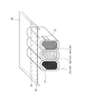
図2は、本発明の実施の形態1に係る発光管アレイの構成を部分的に示す拡大斜視図である。図2に示すように発光管アレイをカラー表示対応とするべく、発光管31ごとに赤色(R)用の蛍光体層36R、緑色(G)用の蛍光体層36G、青色(B)用の蛍光体層36Bを、発光管31の内壁に形成してある。RGB3色の発光管31、31、31を一組として一つの画素を構成することで、カラー表示に対応することができる。
なお、蛍光体層36は、赤色(R)用の蛍光体層36Rでは、ガス放電で発生する紫外線照射により赤色発光する(Y、Gd)BO3 :Eu3+等の蛍光体材料を用いる。緑色(G)用の蛍光体層36Gでは、緑色発光するZn2 SiO4 :Mn等の蛍光体材料を用い、青色(B)用の蛍光体層36Bでは、青色発光するBaMgAl12O17:Eu2+等の蛍光体材料を用いる。これらの蛍光体材料を、スラリーの状態で発光管31となるガラス管に注入して静置することにより、管の下側内壁面に直接蛍光体層36を形成することができる。
本実施の形態1では、発光管31の長手方向に直交する横断面の形状が、長径側を縦にした縦長扁平四辺形状となっており、アドレス電極32が各発光管31の側面に設けられている点に特徴を有する。図3は、本発明の実施の形態1に係る発光管アレイの構成を部分的に示す、発光管31、31、・・・の長手方向に直交する面での断面図である。
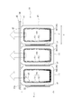
図3に示すように、本実施の形態1に係る発光管アレイの発光管31は、長手方向に直交する横断面の形状が、短径a及び長径bを有し、長径b側を縦にした縦長扁平四辺形状となっている。厳密な意味で扁平四辺形状の横断面を有するガラス管の製造は無理であり、現実的には、発光管31の長手方向に直交する横断面の形状は、短径a側の上下平坦面(第一の平坦面及び第二の平坦面)41、42と長径b側の左右平坦面(第三の平坦面及び第四の平坦面)43及びそれら4つの平坦面の間をつなぐ4つのコーナー部(湾曲面)44を有する擬似八角形状となる。表示面の反対側である第一の平坦面(下部平坦面)41の内側に蛍光体層36が形成され、対向する第二の平坦面(上部平坦面)42に接して表示電極シート35に支持された表示電極対(放電電極対)34が設けられている。
また、本実施の形態1の特徴として、配列方向に隣接する第三の平坦面又は第四の平坦面(側部平坦面)43のいずれか一方に接してアドレス電極32が設けられている。図3では、アドレス電極32は、テープ状のPETフィルム(アドレス電極シート)33に支持されたメッシュパターンの電極構成を有し、各発光管31の左側平坦面(第三の平坦面)43に電極メッシュを通る接着材で張り付けられている。テープ状のPETフィルム33が左側に隣接する発光管31に対して非選択シールド機能を持つ。なお、アドレス電極32は、各発光管31の第三の平坦面43に導電体ペースト(Agペースト)を直接印刷して形成しても良い。この場合、印刷された銀電極膜を保護するとともに、隣接する発光管31に対しての電界侵入強度が低くなるよう電極膜表面をアクリル樹脂等で被覆する。別の構成としてアドレス電極32と対向する第4の平坦面43に電界シールド層を設けるか、隣接する発光管31、31の管璧間に空隙を設けて配列しても良い。また、アドレス電極32を形成する一方の平坦面の管壁の厚さに比べて対向する他方の平坦面の管壁の厚さを厚く形成しておくことによって、隣接する発光管31、31の一方にアドレス電界を有効に印加することも可能となる。
ここで、画素幅を規定する発光管31の断面の短径(幅)aは、高精細化の観点から1mm以下であることが好ましい。この場合、長径(高さ)bが短径aより短くなると蛍光体量が少なくなり、十分な輝度を確保することが困難になる。また、長径(高さ)bが短径aの3倍よりも長くなると、表示電極対34から蛍光体層36までの距離が相対的に長くなり、放電による紫外線の減衰が増加するので、同じく十分な輝度を確保することが困難になる。したがって、短径aと長径bとの関係は3a≧b>aの範囲にあることが好ましい。
発光管31の長手方向に直交する横断面の形状が縦長扁平四辺形状であることにより、発光管31を並置する場合に、発光管31が転倒しにくく、位置決めも容易となる。また、各発光管31の第三の平坦面又は第四の平坦面43のいずれか一方にアドレス電極34を直接形成する場合にも、複数の発光管31の電極形成面となる平坦面を揃えて並べておき、所定の印刷マスクを通して導電体ペーストを印刷することにより容易に一斉形成することが可能となる。
さらに、発光管31の内面には、金属酸化物からなる表面層51と、表面層51から一部が露出している酸化マグネシウム結晶微粒子群52とからなる放電補助膜53を備えている。金属酸化物の表面層は、MgO、CaO、BaO、SrO等のうち、少なくとも1つを含む結晶膜として形成され、表面層51から酸化マグネシウム結晶微粒子群52の一部が露出している。
周期表第2族元素の酸化物は、二次電子放射係数が大きくガス放電空間に面して放電電圧を低減する効果があり、特に酸化マグネシウムは放電面に最も適した材料である。酸化マグネシウムの表面層51と酸化マグネシウム結晶微粒子群52とからなる放電補助膜53の存在により発光管31の管内は放電しやすい状態となる。
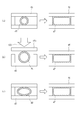
次に、上述した略扁平四辺形状の横断面を有する発光管31の製造工程について説明する。図4は、本発明の実施の形態1に係る発光管アレイの発光管31の製造工程を示す例示図である。
例えば、まず横断面の直径10mm、管厚1.0mm、長さ500mmの硼珪酸系のガラス母管45の両端部を加熱溶融して封止し、内部に空気を密封しておく。
次に、気密にしてあるガラス母管45を成形治具46内に載置する(図4(a)左図参照)。成形治具46は、例えば8.6mm×11.8mmの矩形断面を有し、ガラス母管45が収まるような長さを有しており、材料としてはセラミックス(石英、窒化アルミニウム、窒化ホウ素、窒化珪素、炭化珪素等)を用いることが好ましい。
次に、ガラス母管45を載置した成形治具46を加熱炉(図示せず)内に静置し、640℃まで温度を上昇させる。すると、ガラス母管45内の空気が膨張して内圧が上昇するとともにガラス母管45自体が軟化するので、ガラス母管45は、成形治具46の内面の形状に沿った形状(横断面が縦長扁平四辺形状)に変形する。
変形したガラス母管45を成形治具46内に載置したまま冷却することで、横断面が縦長扁平四辺形状のガラス管プリフォーム47が完成する(図4(a)右図参照)。冷却時には、ガラス母管45の方がガラス母管45の内部の空気よりも先に冷却されるので、ガラス管プリフォーム47はその形状を維持することができる。
なお、ガラス母管45は、直径が成形治具46の内面の高さより大きく、成形治具46内に収まらない大きさであっても良い。この場合、ガラス母管45を載置した成形治具46は、成形治具46の上蓋46aが成形治具46の他の部分から離れた状態で加熱炉内に静置され、上蓋46aの上方から一定の圧力100を加えてガラス母管45を軟化させる(図4(b)左図参照)。これにより、ガラス母管45は、成形治具46の内面の形状に沿った形状(横断面が縦長扁平四辺形状)に変形し、変形したガラス母管45を成形治具46内に載置したまま冷却することで、横断面が縦長扁平四辺形状のガラス管プリフォーム47が完成する(図4(b)右図参照)。
また、横断面が予め縦長扁平四辺形状に成型してあるガラス母管48を用いて、同様に横断面が縦長扁平四辺形状のガラス管プリフォーム47を成形しても良い(図4(c)参照)。このようにして成形されたガラス管プリフォーム47を、次の工程でリドローして所定寸法まで線引きすることにより、相似断面を有する発光管31の外囲器となるガラス管を作製する。作製されたガラス管を所定の長さに切断し、引き続き放電保護膜の形成、蛍光体層の形成、ガス封入及び封止等のプロセス等を経て発光管31を作製することができる。
以上のように本実施の形態1によれば、発光管31は、長手方向に直交する横断面の形状が、長径b側を縦にした縦長扁平四辺形状であり、長径b側の管壁が互いに隣接するように並置して発光管アレイを構成している。発光管31の長手方向に直交する横断面の形状を縦長扁平四辺形状(厳密には疑似八角形状)とした場合、発光管31と表示電極34との接触面積を十分に確保して安定した放電特性を得ることができ、しかも短径a側の管径寸法を短くしたにも関わらず発光管31の容積は減らないので内壁に形成する蛍光体層36の表面積が実質的に減少することがない。したがって、一定の輝度を確保しつつ画素のサイズが3mm以下という高精細の発光管アレイ型カラー表示装置を提供することが可能となる。
また、実施の形態1の構成においては、表示電極34と接する第二の平坦面(上部平坦面)42と、アドレス電極32と接する第三の平坦面(側部平坦面)43との間のコーナー部(湾曲面)44aで、矢印45に示すようにアドレス放電(選択放電)が発生する。両電極間の放電ギャップの距離が短くなることから、リセット放電電圧やアドレス放電電圧の上昇を招くことがなく、横断面が横長扁平形状の発光管を並置した発光管アレイと同等又はそれ以下の電圧で駆動することが可能となる。ちなみに、1mmの長径を挟んだ対向放電電圧は120~150Vとなるが、本発明によるコーナー放電型の斜め対向放電電圧は同じサイズの発光管31において50~70Vと大幅に低下する。
なお、発光管31は、蛍光体層36を形成した蛍光体支持部材(ボート)をガラス管の中に挿入して構成しても良い。図5は、本発明の実施の形態1に係る発光管アレイの各発光管31の中に、樋状(U字状)断面を有する蛍光体支持部材を挿入して蛍光体層36を設けた場合の長手方向に直交する面での断面図である。この場合、長径を挟む対抗放電形式であれば、蛍光体支持部材の挿入によってアドレス電圧が大きく上昇する。しかし、コーナー放電型においては、蛍光体支持部材によるアドレス放電電圧への影響はほとんど見られない。
図5に示すように、蛍光体支持部材50は、短径側の第一の平坦面41を底にした樋状(U字状)断面を有し、蛍光体層36は、蛍光体支持部材50の内面上に形成される。蛍光体支持部材50の長径方向の長さb2は、発光管31の長径b1よりも短いが、十分な輝度を確保するためには長径b1の半分以上、好ましくは3分の2よりも長いことが好ましい。
(実施の形態2)
本発明の実施の形態2に係る発光管アレイでは、発光管31は、表示電極34、34、・・・が配列方向に隣接する二つの発光管で共用するように各発光管31の長径側の左右いずれか一方の平坦面に接して設けられており、アドレス電極32、32、・・・が短径側の下部平坦面に接して設けられている点で、実施の形態1とは相違する。隣接する二つの発光管31で共用される表示電極34は交互にX電極、Y電極として機能する。
本発明の実施の形態2に係る発光管アレイでは、発光管31は、表示電極34、34、・・・が配列方向に隣接する二つの発光管で共用するように各発光管31の長径側の左右いずれか一方の平坦面に接して設けられており、アドレス電極32、32、・・・が短径側の下部平坦面に接して設けられている点で、実施の形態1とは相違する。隣接する二つの発光管31で共用される表示電極34は交互にX電極、Y電極として機能する。
図6は、本発明の実施の形態2に係る発光管アレイの構成を部分的に示す、発光管31、31、・・・の長手方向に直交する面での断面図である。図6では、実施の形態1と同等の部分には同一の符号を付している。図6に示すように、本実施の形態2に係る発光管アレイの発光管31も、長手方向に直交する横断面の形状が、長径b側を縦にした縦長扁平四辺形状となっている。
図6では、擬似八角形状の横断面を有する各発光管31の長径b側の一の平坦面(第三の平坦面又は第四の平坦面)43に長手方向に沿って放電電極34a、34bが形成されており、それぞれ背中合わせに隣接する二つの発光管31、31に共用されている。放電電極34aと放電電極34bとは交互にX電極、Y電極として機能するので、両電極間に放電電圧パルスを交互に印加することにより、短径寸法の対向放電間隙を横に挟んだ形で維持放電が発生する。また、X電極として機能する放電電極34aを交互に隣接するX電極群X1とX電極群X2との2群に分け、Y→X1→Y→X2の順に放電電圧パルスを印加することにより、奇数番目の発光管群(例えばX電極群X1)と偶数番目の発光管群(例えばX電極群X2)とを交互に発光させることができる。
また、隣接する発光管31、31の間で共用する放電電極34a、34bは、予め各発光管31の両側に印刷形成した導電膜を背中合わせにコンタクトさせて構成することもできる。この場合、隣接する導電膜間を導電性接着材又は導電性テープで接着しても良い。
さらに、複数のアドレス電極32、32、・・・は、アドレス電極シート33の上に発光管31を横切る方向に形成されていて、各発光管31の第一の平坦面41に接して設けられている。つまり、アドレス電極32は、発光管31の蛍光体層36を備える側の平坦面に接して設けられている。したがって、アドレス放電は、アドレス電極32と2本おきに隣接する二つの発光管31の間でY電極として機能する放電電極34bとの間のコーナー部(湾曲面)44bで矢印45に示すように発生する。この場合、X電極として機能する放電電極34aを交互に隣接するX電極群X1とX電極群X2との2群に分けてアドレス電界をキャンセルする極性の電圧を選択的に印加しておくことで、Y電極として機能する放電電極34bを走査電極として共用する二つの発光管31、31を交互に分割アドレスし、いわゆるインタレース駆動を行うことが可能となる。
以上のように本実施の形態2によれば、アドレス電極32が延伸するアドレス電極シート33をアレイ配列面の背面側に設けて、前面側には発光を遮るものがない構成となるので、蛍光体層36からの光を点線矢印のように前面側から効率的に取り出すことができる。この構成において、全ての発光管31の蛍光体層36を例えばGdを含んだ紫外線発光蛍光体材料を用いて形成しておくことにより、紫外線光源としてのフィルム状の発光管アレイを得ることができる。
(実施の形態3)
本発明の実施の形態3に係る発光管アレイは、表示電極34、34、・・・として、一対のX電極34a、Y電極34bが発光管31ごとに配置されており、隣接する発光管31、31の間に絶縁層を設けてある点で実施の形態2とは相違する。
本発明の実施の形態3に係る発光管アレイは、表示電極34、34、・・・として、一対のX電極34a、Y電極34bが発光管31ごとに配置されており、隣接する発光管31、31の間に絶縁層を設けてある点で実施の形態2とは相違する。
図7は、本発明の実施の形態3に係る発光管アレイの構成を部分的に示す、発光管31、31、・・・の長手方向に直交する面での断面図である。図7では、実施の形態1及び2と同等の部分には同一の符号を付している。図7に示すように、本実施の形態3に係る発光管アレイの発光管31も、長手方向に直交する横断面の形状が、長径b側を縦にした縦長扁平四辺形状となっている。
実施の形態3においては、各発光管31の長径b側の第三の平坦面及び第四の平坦面(側部平坦面)43、43に、それぞれX電極34a、Y電極34bが発光管31ごとに設けてある。また、複数のアドレス電極32、32、・・・は、実施の形態2の場合と同様に、アドレス電極シート33の上に発光管31を横切る方向に発光管31の第一の平坦面41に接して設けられている。
つまり、実施の形態3の構成では、実施の形態2とは異なり、表示電極34、34、・・・として、一対のX電極34a、Y電極34bが発光管31ごとに配置されており、隣接する発光管31、31の間には、X電極34aとY電極34bとの短絡を防止するべく、仲介絶縁層60を設けてある。ただし、仲介絶縁層60内での電力損失を最小化するよう、隣接する発光管31、31の放電タイミングを交互にずらして駆動することが好ましい。なお、本実施の形態3におけるX電極34a及びY電極34bは、上述のように発光管31の側面に直接形成する代わりに、帯状の支持体の両側に帯状導体膜を形成した電極構体を作成し、作成された電極構体を、隣接する発光管31、31の側部平坦面間に挟み込んで発光管アレイを構成することもできる。容易に、しかも強固に接着するためには、帯状導体膜はメッシュパターンが好ましい。
また、以上の実施例においては、横断面が縦長扁平四辺形状の発光管31の長径を縦にして並置した発光管アレイを中心に説明しているが、コーナー部44でのアドレス放電を可能とする本発明の電極配置は、同様に横断面が縦長扁平四辺形状の発光管31の長径を横に並置した場合でもアドレス放電電圧が低くなる効果が得られるので、安定した確実な駆動を実現する上で有益である。その他、本発明の趣旨の範囲内であれば上述した実施の形態に限定されるものではなく、多種の変形、置換等が可能である。
31、31R、31G、31B 発光管
32 アドレス電極
33 アドレス電極シート(絶縁テープ)
34 表示電極(対)(放電電極)
34a X電極、放電電極
34b Y電極、放電電極
35 表示電極シート
41 第一の平坦面
42 第二の平坦面
43 第三の平坦面、第四の平坦面
44、44a、44b 湾曲面
50 蛍光体支持部材
51 表面層
52 酸化マグネシウム結晶微粒子群
53 放電補助膜
60 仲介絶縁層
32 アドレス電極
33 アドレス電極シート(絶縁テープ)
34 表示電極(対)(放電電極)
34a X電極、放電電極
34b Y電極、放電電極
35 表示電極シート
41 第一の平坦面
42 第二の平坦面
43 第三の平坦面、第四の平坦面
44、44a、44b 湾曲面
50 蛍光体支持部材
51 表面層
52 酸化マグネシウム結晶微粒子群
53 放電補助膜
60 仲介絶縁層
Claims (6)
- 並置して配列された複数の発光管と、
該発光管を横切る方向に延伸する第1の電極群と、
各発光管の長手方向に沿って設けられた第2の電極群と
を備え、
前記発光管が略扁平四辺形状の横断面を有し、
前記第1の電極群が各発光管の一の平坦面に接して設けられ、前記第2の電極群が各発光管の前記一の平坦面に隣接した側方の平坦面に接して設けられていることを特徴とする発光管アレイ。 - 前記第1の電極群が放電電極対として各発光管の短径側の一の平坦面に接し、第2の電極群がアドレス電極として長径側の一の平坦面に接していることを特徴とする請求項1に記載の発光管アレイ。
- 前記第1の電極群がアドレス電極として各発光管の短径側の一の平坦面に接し、前記第2の電極群が放電電極対として各発光管の長径側の少なくとも一の平坦面に接していることを特徴とする請求項1に記載の発光管アレイ。
- 前記第2の電極群は、隣接する二つの発光管で共有されていることを特徴とする請求項3に記載の発光管アレイ。
- 前記第2の電極群が放電電極対として各発光管の長径側の対向する両側の平坦面に設けられていることを特徴とする請求項3に記載の発光管アレイ。
- 前記発光管は、長手方向に直交する横断面の形状が、短径側の対向する第一及び第二の平坦面と、長径側の対向する第三及び第四の平坦面、及びこれら4つの平坦面の間をつなぐ4つの湾曲面を有する縦長扁平の疑似八角形状であることを特徴とする請求項1乃至5のいずれか一項に記載の発光管アレイ。
Applications Claiming Priority (2)
| Application Number | Priority Date | Filing Date | Title |
|---|---|---|---|
| JP2013-050220 | 2013-03-13 | ||
| JP2013050220A JP2014175294A (ja) | 2013-03-13 | 2013-03-13 | 発光管アレイ |
Publications (1)
| Publication Number | Publication Date |
|---|---|
| WO2014142140A1 true WO2014142140A1 (ja) | 2014-09-18 |
Family
ID=51536792
Family Applications (1)
| Application Number | Title | Priority Date | Filing Date |
|---|---|---|---|
| PCT/JP2014/056399 Ceased WO2014142140A1 (ja) | 2013-03-13 | 2014-03-12 | 発光管アレイ |
Country Status (2)
| Country | Link |
|---|---|
| JP (1) | JP2014175294A (ja) |
| WO (1) | WO2014142140A1 (ja) |
Citations (7)
| Publication number | Priority date | Publication date | Assignee | Title |
|---|---|---|---|---|
| JPH02288061A (ja) * | 1989-03-29 | 1990-11-28 | Asea Brown Boveri Ag | 高出力放射器 |
| JP2003092085A (ja) * | 2001-09-17 | 2003-03-28 | Fujitsu Ltd | 表示装置 |
| WO2005055267A1 (ja) * | 2003-12-01 | 2005-06-16 | Fujitsu Limited | 発光管アレイ型表示装置およびその駆動方法 |
| JP2005191016A (ja) * | 2005-03-10 | 2005-07-14 | Fujitsu Ltd | 発光体および表示装置 |
| JP2005209637A (ja) * | 2003-12-24 | 2005-08-04 | Toray Ind Inc | プラズマディスプレイ部材およびプラズマディスプレイ |
| JP2009520322A (ja) * | 2005-12-12 | 2009-05-21 | レイセオン・サルコス・エルエルシー | マルチセル電子回路配列及び製造方法 |
| JP2013118070A (ja) * | 2011-12-02 | 2013-06-13 | Shinoda Plasma Kk | 発光管アレイ型表示装置 |
-
2013
- 2013-03-13 JP JP2013050220A patent/JP2014175294A/ja not_active Withdrawn
-
2014
- 2014-03-12 WO PCT/JP2014/056399 patent/WO2014142140A1/ja not_active Ceased
Patent Citations (7)
| Publication number | Priority date | Publication date | Assignee | Title |
|---|---|---|---|---|
| JPH02288061A (ja) * | 1989-03-29 | 1990-11-28 | Asea Brown Boveri Ag | 高出力放射器 |
| JP2003092085A (ja) * | 2001-09-17 | 2003-03-28 | Fujitsu Ltd | 表示装置 |
| WO2005055267A1 (ja) * | 2003-12-01 | 2005-06-16 | Fujitsu Limited | 発光管アレイ型表示装置およびその駆動方法 |
| JP2005209637A (ja) * | 2003-12-24 | 2005-08-04 | Toray Ind Inc | プラズマディスプレイ部材およびプラズマディスプレイ |
| JP2005191016A (ja) * | 2005-03-10 | 2005-07-14 | Fujitsu Ltd | 発光体および表示装置 |
| JP2009520322A (ja) * | 2005-12-12 | 2009-05-21 | レイセオン・サルコス・エルエルシー | マルチセル電子回路配列及び製造方法 |
| JP2013118070A (ja) * | 2011-12-02 | 2013-06-13 | Shinoda Plasma Kk | 発光管アレイ型表示装置 |
Also Published As
| Publication number | Publication date |
|---|---|
| JP2014175294A (ja) | 2014-09-22 |
Similar Documents
| Publication | Publication Date | Title |
|---|---|---|
| JP2001345054A (ja) | プラズマディスプレイ装置 | |
| CN100483604C (zh) | 等离子体显示装置 | |
| JP2003272562A (ja) | ガス放電管及びそれを用いた表示装置 | |
| JP5189025B2 (ja) | 表示装置 | |
| US7816850B2 (en) | Display device including gas discharge tubes, and method of manufacturing display device | |
| WO2014142140A1 (ja) | 発光管アレイ | |
| US7687993B2 (en) | Image display | |
| JP2013118070A (ja) | 発光管アレイ型表示装置 | |
| US20070108906A1 (en) | Plasma display panel (PDP) and plasma display apparatus including the PDP | |
| JP4368870B2 (ja) | プラズマディスプレイパネル | |
| KR100768188B1 (ko) | 플라즈마 디스플레이 패널 | |
| CN100530502C (zh) | 等离子体显示面板 | |
| KR100634710B1 (ko) | 플라즈마 디스플레이 패널의 제조방법 | |
| KR100970403B1 (ko) | 플라즈마 디스플레이 패널 | |
| JP2004241387A (ja) | プラズマディスプレイパネル | |
| KR100730142B1 (ko) | 플라즈마 디스플레이 패널 | |
| KR100759561B1 (ko) | 플라즈마 디스플레이 패널 | |
| KR100813837B1 (ko) | 플라즈마 디스플레이 패널 | |
| JPWO2006112419A1 (ja) | プラズマディスプレイパネル | |
| JP2009152190A (ja) | プラズマディスプレイパネルおよびその製造方法 | |
| US20070158687A1 (en) | Base substrate, method of separating the base substrate and plasma display panel using the same | |
| KR100892826B1 (ko) | 플라즈마 디스플레이 패널과 그 제조 방법 | |
| JP2004349058A (ja) | プラズマディスプレイパネル | |
| JP2002184316A (ja) | プラズマディスプレイパネル用基板、プラズマディスプレイパネル及びプラズマディスプレイ装置 | |
| JP2005056732A (ja) | プラズマディスプレイパネルの製造方法 |
Legal Events
| Date | Code | Title | Description |
|---|---|---|---|
| 121 | Ep: the epo has been informed by wipo that ep was designated in this application |
Ref document number: 14764239 Country of ref document: EP Kind code of ref document: A1 |
|
| NENP | Non-entry into the national phase |
Ref country code: DE |
|
| 122 | Ep: pct application non-entry in european phase |
Ref document number: 14764239 Country of ref document: EP Kind code of ref document: A1 |