WO2014132843A1 - 信号処理装置および信号処理方法 - Google Patents
信号処理装置および信号処理方法 Download PDFInfo
- Publication number
- WO2014132843A1 WO2014132843A1 PCT/JP2014/053813 JP2014053813W WO2014132843A1 WO 2014132843 A1 WO2014132843 A1 WO 2014132843A1 JP 2014053813 W JP2014053813 W JP 2014053813W WO 2014132843 A1 WO2014132843 A1 WO 2014132843A1
- Authority
- WO
- WIPO (PCT)
- Prior art keywords
- clock signal
- data
- signal
- timing error
- timing
- Prior art date
- Legal status (The legal status is an assumption and is not a legal conclusion. Google has not performed a legal analysis and makes no representation as to the accuracy of the status listed.)
- Ceased
Links
Images





Classifications
-
- G—PHYSICS
- G06—COMPUTING OR CALCULATING; COUNTING
- G06F—ELECTRIC DIGITAL DATA PROCESSING
- G06F1/00—Details not covered by groups G06F3/00 - G06F13/00 and G06F21/00
- G06F1/04—Generating or distributing clock signals or signals derived directly therefrom
- G06F1/12—Synchronisation of different clock signals provided by a plurality of clock generators
-
- H—ELECTRICITY
- H03—ELECTRONIC CIRCUITRY
- H03K—PULSE TECHNIQUE
- H03K5/00—Manipulating of pulses not covered by one of the other main groups of this subclass
- H03K5/153—Arrangements in which a pulse is delivered at the instant when a predetermined characteristic of an input signal is present or at a fixed time interval after this instant
- H03K5/1534—Transition or edge detectors
Definitions
- the present invention relates to a signal processing device and a signal processing method.
- the data output from the sending flip-flop is arithmetically processed by the arithmetic circuit and then received.
- a synchronous system is known in which the operation of transferring to the flip-flop on the side is performed in synchronization with a clock signal.
- Such a signal processing device is designed so that the flip-flop can operate in synchronization with the rising edge of the clock signal, and during the one cycle from the rising edge of the clock signal to before the next rising edge, The data is transferred from the flip-flop to the receiving flip-flop via the arithmetic circuit.
- the processing time of the critical path in the arithmetic circuit provided between the flip-flops is 12 [ns]
- the period of one clock from the rising edge of the clock signal to the next rising edge is 12 [ns]
- the data that has reached the receiving flip-flop via the arithmetic circuit from the sending flip-flop is synchronized with a clock cycle different from the clock cycle of the clock signal. Compare the data from the sending flip-flop via the arithmetic circuit to the receiving flip-flop, and when these two data do not match, the processing time of the data becomes long in the arithmetic circuit and a timing error occurs.
- the timing error detection circuit having such a configuration, since the timing error in the arithmetic circuit is detected afterwards, data processing is already performed in other circuits with erroneous data in which the timing error has occurred in the arithmetic circuit. Therefore, it is difficult to correct data in each circuit. For this reason, considering the time for correcting data in each circuit, the final calculation processing result in the arithmetic circuit is not analyzed afterwards as in the past, but the arithmetic circuit has the correct timing in the middle of the arithmetic processing in the arithmetic circuit. It is preferable that it can be estimated whether or not it is operating.
- An object of the present invention is to propose a signal processing apparatus and a signal processing method capable of estimating whether or not the signal is being processed.
- data being processed is acquired from a logic circuit that processes and outputs data at a predetermined timing in synchronization with a predetermined clock signal. It is characterized in that it is determined whether the timing of the data is shifted with respect to the clock signal at an intermediate stage.
- the present invention if data is already out of timing with respect to the clock signal in the middle of processing in the logic circuit, it can be assumed that the processing cannot be completed within the time assumed by the logic circuit, and thus the logic circuit. It is possible to infer whether or not the logic circuit is operating at the correct timing in the middle stage of the logic circuit processing without analyzing the final processing result in FIG.
- FIG. 6A is a schematic diagram illustrating a circuit configuration of a detection clock signal generation circuit
- FIG. 6B is a timing chart of a clock signal, a delayed clock signal, and a detection clock signal.
- 4 is a timing chart of a detection clock signal, data, an estimated timing error signal, and a gating clock signal.
- FIG. 11A is a schematic diagram illustrating a circuit configuration of a signal integration determination unit
- FIG. 11B is a schematic diagram illustrating a circuit configuration of a signal integration determination unit according to another embodiment. It is the schematic which shows the circuit structure (1) of the signal processing apparatus by other embodiment provided with the signal integration determination part. It is the schematic which shows the circuit structure (2) of the signal processing apparatus by other embodiment provided with the signal integrated determination part.
- reference numeral 1 denotes a signal processing apparatus of the present invention.
- a multiplier 4 is provided as a logic circuit between a sending flip-flop 2 and a receiving flip-flop 3. , And the data D output from the sending flip-flop 2 in synchronization with the clock signal CK can be multiplied by the multiplier 4 and then output to the receiving flip-flop 3.
- the multiplier 4 is composed of a first logic block 5a and a second logic block 5b composed of a plurality of logic gates, and is processed in the first logic block 5a in synchronization with the clock signal CK. Data obtained by multiplying the data D by the second logical block 5b is obtained.
- the multiplier 4 has a checkpoint C in which the timing error estimation unit 7 is connected between the first logic block 5a and the second logic block 5b, and is processed in the first logic block 5a. Data D can be sent to the timing error estimation unit 7.
- the multiplier 4 has the same processing time in the critical path that is the longest processing path as the period of one clock of the clock signal CK (for example, 12 [ns]). .
- the multiplier 4 is set to the rising period H1 (the period from the rising edge to the falling edge, here 6 [ns]) of the first half of one clock in the processing time in the first logic block 5a.
- the processing time of the second logic block 5b is set to the falling period L1 (the period from the falling edge to the rising edge, here 6 [ns]) of the second half of one clock.
- the clock signal CK repeats the rising period H1 and the falling period L1 alternately in order, and the rising period H1 and the falling period L1 having a duty ratio of 50% constitute one clock.
- the multiplier 4 synchronizes the arithmetic processing of the first logic block 5a and the second logic block 5b with the clock signal CK, and even when the data D passes through the critical path. It must be completed within the period of one clock. Therefore, the arithmetic processing of the first logic block 5a must be completed before the falling edge of the first half end of the clock signal CK (during the rising period H1). I must.
- the timing error estimation unit 7 extracts the data D processed in the first logic block 5a from the multiplier 4 via the check point C which is an intermediate point, and at that time, the operation of the first logic block 5a It is determined whether or not the processing is completed before the falling edge at the end of the first half of the clock signal CK (during the rising period H1).
- the timing error estimator 7 is configured so that when the arithmetic processing of the first logical block 5a is performed after the falling edge of the clock signal CK, the arithmetic processing combining the first logical block 5a and the second logical block 5b is 1 It can be determined that the timing does not end within the clock period, and it can be assumed that the multiplier 4 generates a timing error.
- the timing error estimation unit 7 includes a transition detection unit 8 that detects a transition of the data D at the check point C, and a transition of the data D detected by the transition detection unit 8 during the falling period L1 of the clock signal CK. And an error determination unit 9 for determining whether or not.
- the transition detection unit 8 has a negative exclusive OR circuit 12, and the data D during the processing of the multiplier 4 obtained at the checkpoint C is negatively exclusive via the delay circuits 11a and 11b. While inputting to one input part of the OR circuit 12, the data D in the middle of processing of the multiplier 4 obtained at the check point C can be input to the other input part of the negative exclusive OR circuit 12 as it is.
- the negative exclusive OR circuit 12 performs a negative exclusive OR of the delayed data input from one input unit and the data D input from the other input unit, and outputs the resulting data to the error determination unit 9 To do.
- the negative exclusive OR circuit 12 generates an error from the output unit when the delayed data and the data D both fall, and when both rise, the data “1” indicating that the data D has not changed It can be output to the determination unit 9.
- the negative exclusive OR circuit 12 displays one of the delayed data before the transition.
- the data D after the transition is input to the other input unit as it is, and the negative exclusive OR of the delay data and the data D is taken, and “0” data indicating that the data D has transitioned is obtained.
- the output can be output to the error determination unit 9.
- the error determination unit 9 includes an AND circuit 14 in which one input unit is connected to the output unit of the negative exclusive OR circuit 12, and an output unit of the AND circuit 14 is connected to one input unit.
- the clock signal CK is input to the other input section
- the output section includes a negative OR circuit 15 connected to the other input section of the AND circuit 14.
- the negative OR circuit 15 has the clock signal CK input to the other input unit, and the “0” data from the logical product circuit 14 input from one input unit is the rising period H1 of the clock signal CK, or It can be determined at which timing of the falling period L1. For example, when the “0” data is input from the logical product circuit 14 to one input unit, the negative logical sum circuit 15 has the first signal when the clock signal CK of the falling period L1 is input to the other input unit. Since processing of data D in 1 logic block 5a has not been completed before the falling edge of the first half of 1 clock, processing of data D by multiplier 4 can still be processed within 1 clock.
- the estimated timing error signal STE (in this case, “1” data) indicating that a timing error may occur may be output from the output unit.
- the error determination unit 9 outputs the estimated timing error signal STE to the other input unit of the AND circuit 14. Although “0” data is input to one input section of the AND circuit 14, “0” data continues to be output from the output section of the AND circuit 14.
- the negative logical sum circuit 15 is connected to the second input unit when the clock signal CK of the rising period H1 is input to the other input unit.
- the processing of data D was completed before the falling edge of the first half of one clock, so that the processing of data D by multiplier 4 could be processed within 1 clock.
- the indicated “0” data can be output from the output unit.
- the clock signal control unit 17 that gates the clock signal CK based on the “1” data output from the timing error estimation unit 7 includes the timing error estimation unit 7. Connected to the output.
- the clock signal control unit 17 includes a latch circuit 19 and a logical product circuit 20, and for example, the estimated timing error signal STE output from the timing error estimation unit 7 can be input to the latch circuit 19.
- the latch circuit 19 is input with an inverted clock signal in which the rising and falling edges of the clock signal CK are inverted, and is configured to detect the cycle of one clock in the clock signal CK.
- the latch circuit 19 has the AND circuit 20 connected to the output unit, and once receives the estimated timing error signal STE ("1" data) from the timing error estimating unit 7, the next rising edge in the clock signal CK is received. Can be output to the AND circuit 20 as it is.
- the clock signal CK is input to one input unit and the data from the latch circuit 19 is input to the other input unit.
- the logic of the clock signal CK and the data from the latch circuit 19 is input.
- the gating clock signal GCK obtained as a result can be output to the sending flip-flop 2 and the receiving flip-flop 3.
- the sending flip-flop 2 and the receiving flip-flop 3 can operate in synchronization with the gating clock signal GCK received from the clock signal control unit 17.
- the AND circuit 20 does not change the value of “0” even if the clock signal CK rises as long as “0” data obtained by inverting the “1” data output from the latch circuit 19 is input to the other input unit. ”Continues to output data and gates the clock signal CK to the sending flip-flop 2 and the receiving flip-flop 3 so that the falling state is maintained without causing the next rising edge.
- the timing clock signal GCK can be output.
- the latch circuit 19 receives the “0” data from the timing error estimation unit 7 and receives the “0” data when the clock signal CK in which the rising edge of the next one clock after the gated one clock is generated is input. It can be output to the AND circuit 20.
- the AND circuit 20 receives “1” data obtained by inverting the “0” data at the other input section connected to the latch circuit 19, and the rising clock signal CK at one input section. By taking the logical product of both of these, the gating clock signal GCK can be raised and output to the flip-flop 2 on the sending side and the flip-flop 3 on the receiving side.
- the sending flip-flop 2 and the receiving flip-flop 3 are gated and do not rise, and then follow the rising period H1 of one clock.
- the rising period H1 of one clock is supplied based on the gating clock signal GCK, and the processing operation can be executed in synchronization with one clock whose cycle is doubled (24 [ns]).
- the multiplier 4 can operate at the correct timing in synchronization with the new rising period H1 of the clock signal CK (gating clock signal GCK), and outputs the correct data D to the flip-flop 3 on the receiving side.
- the receiving flip-flop 3 can also be prevented from operating due to erroneous data due to a timing error.
- the clock signal CK is a pulse-like signal that alternately repeats the rising period H1 and the falling period L1.
- a period Tck1 of one clock is constituted by the rising period H1 in the first half and the falling period L1 in the second half.
- the arithmetic processing in the first logic block 5a takes more time than expected, and the arithmetic processing in the first logic block 5a is performed before the falling edge of the first half end of the clock signal CK (rising period H1 Middle) shows data D that has not ended.
- the timing error estimation unit 7 detects a transition of data D during the falling period L1 of the clock signal CK.
- the estimated timing error signal STE is reset when the clock signal CK rises, and as a result, during the time Err from the transition point of the data D detected by the transition detection unit 8 to the rising edge of the clock signal CK. Can occur.
- the gating clock signal GCK generated by the clock signal controller 17 is a clock signal from the generation of the estimated timing error signal STE to the next one clock rising period H1 (indicated as “CG” in FIG. 2).
- the falling period L1 can be maintained as it is without gating CK and generating the rising period H1 immediately after the generation of the estimated timing error signal STE.
- FIG. 3 is a timing chart showing a result of spice simulation when the estimated timing error signal STE is continuously generated.
- the estimated timing error signal STE is continuously generated accordingly.
- the clock signal CK is gated from the generation of the first estimated timing error signal STE to the falling edge of the clock signal CK immediately thereafter, the clock immediately after the generation of the estimated timing error signal STE is continued.
- the gating clock signal GCK in which the clock signal CK is gated again is generated.
- the signal processing device 1 gates the clock signal CK from the generation of the estimated timing error signal STE until the falling edge of the clock signal CK immediately thereafter until the estimated timing error signal STE is not detected, and the multiplier 4 The normal operation synchronized with the rising period H1 of the clock signal CK (gating clock signal GCK) in FIG.
- the signal processing apparatus 1 acquires the data D being processed from the multiplier 4 that processes and outputs the data D at a predetermined timing in synchronization with the predetermined clock signal CK, A timing error estimation unit 7 for determining whether or not the data D is out of timing with respect to the clock signal CK is provided.
- the timing of the data D is already shifted from the clock signal CK in the middle of processing in the multiplier 4, the time assumed by the multiplier 4 (in this case, a period of 12 [ns of one clock) ]) Within the middle of the arithmetic processing of the multiplier 4 without analyzing the final arithmetic processing result in the multiplier 4 afterwards. It can be estimated whether or not it is operating at the correct timing.
- the signal processing device 1 when the timing error estimation unit 7 estimates that the data D is out of timing with respect to the clock signal CK in the multiplier 4, the clock signal control unit 17 CK is gated, and the supply of the clock signal CK to the multiplier 4 is controlled. As described above, the signal processing device 1 can reflect the estimation result of the timing error occurrence obtained in the timing error estimation unit 7, and can gate the clock signal CK to the multiplier 4, thereby receiving the receiving side. It is possible to prevent the flip-flop 3 from operating due to erroneous data having a timing error.
- the number of cycles of the clock signal CK required for multiplication by the multiplier 4 is represented by ⁇ , and the throughput is represented by ⁇ . From FIG. 4, the throughput was improved up to the cycle time 8.2 [ns] of the clock signal CK. If the cycle time of the clock signal CK is made smaller than 9 [ns], the number of cycles gradually increases due to the gating of the clock signal CK by the clock signal control unit 17, and the throughput decreases accordingly. Was confirmed. However, when the cycle time of the clock signal CK is 6.4 [ns], the throughput is not improved, but the same throughput as that of the cycle time 10.8 [ns] of the clock signal CK is obtained, and it was confirmed that the clock signal CK operates normally.
- the timing error estimation unit 37 determines whether the processing of the data D by the first logical block 35a is completed within 8 [ns] based on the data D obtained from the checkpoint C. As a result, when the processing of the data D by the first logical block 35a exceeds 8 [ns], it can be estimated that a timing error has occurred.
- the timing error estimation unit 37 is different from the above-described first embodiment in that the error determination unit 39 includes a detection clock signal generation circuit 40, and the detection clock signal generation is performed.
- the circuit 40 can generate a detection clock signal DCK from which a timing error can be estimated at checkpoint C.
- the error determination unit 39 has a configuration in which the output of the detection clock signal generation circuit 40 is connected to the other input unit of the negative OR circuit 15, and the detection generated by the detection clock signal generation circuit 40.
- the logical OR of the clock signal DCK and the data from the AND circuit 14 is taken, and the resulting data can be output to the clock signal control unit 17.
- the clock signal CK is input to one input unit, and the delay clock is input to the other input unit via delay circuits 41a, 41b, 41c, 41d.
- An OR circuit 43 to which the signal Delayed_CK is input is provided.
- the delay amount of the clock signal CK by the delay circuits 41a, 41b, 41c, and 41d is selected according to the position of the check point C.
- the clock signal CK has a rising period and a falling period of 6 [ns], so that the delay circuits 41a, 41b, 41c, 41d 2 [ns] is selected as the delay amount Td for delaying the delay time, and a delayed clock signal Delayed_CK is generated by delaying the clock signal CK by 2 [ns].
- the logical sum circuit 43 generates the detection clock signal DCK in the rising period H2 of 8 [ns] which is the same as the processing time of the first logical block 35a by taking the logical sum of the clock signal CK and the delayed clock signal Delayed_CK. This can be output to the NOR circuit 15.
- the negative OR circuit 15 assumes processing in the first logic block 35a when there is a falling or rising transition of the data D during the falling period L2 of the detection clock signal DCK.
- the estimated timing error signal STE can be output to the clock signal control unit 17 on the assumption that a timing error has occurred over time (in this case, 8 [ns]).
- the clock signal control unit 17 has the same configuration as that of the first embodiment described above.
- the clock signal control unit 17 receives the estimated timing error signal from the timing error estimation unit 37, the clock signal control unit 17 and the first embodiment described above.
- a gating clock signal GCK obtained by gating the clock signal CK can be generated and output to the flip-flop 2 on the sending side and the flip-flop 3 on the receiving side.
- the sending flip-flop 2 and the receiving flip-flop 3 generate a new clock based on the gating clock signal GCK when the timing error estimation unit 37 stops generating the estimated timing error signal STE. Then, the processing operation can be executed in synchronization with the rising edge of one clock.
- the multiplier 34 can operate normally in synchronization with the rising period of the clock signal CK (gating clock signal GCK), outputs correct data D to the receiving flip-flop 3, and further receives the flip-flop on the receiving side. 3 can also prevent malfunctions due to erroneous data.
- timing error estimation correction processing will be briefly described with reference to the timing chart shown in FIG.
- the rising period H2 and the falling period L2 are adjusted to the processing time of the first logic block 35a and the processing time of the second logic block 35b, respectively.
- the arithmetic processing in the first logical block 35a takes longer than expected, and the arithmetic processing in the first logical block 35a is completed before the falling edge of the detection clock signal DCK (within 8 [ns]).
- the timing error estimating unit 37 detects the transition of the data D during the falling period L2 of the detection clock signal DCK.
- the estimated timing error signal STE is reset when the detection clock signal DCK rises, and as a result, the time from the transition point of the data D detected by the transition detection unit 8 to the rising edge of the detection clock signal DCK Can occur during Err.
- the gating clock signal GCK generated by the clock signal control unit 17 is a clock signal from the generation of the estimated timing error signal STE to the next one clock rising period H2 (indicated as “CG” in FIG. 7).
- the falling period L2 can be maintained as it is without gating CK and generating the rising period H2 immediately after the generation of the estimated timing error signal STE.
- the signal processing device 31 also gates the clock signal CK from the generation of the estimated timing error signal STE to the falling edge of the clock signal CK immediately thereafter, and the multiplier 34 synchronizes with the rising period H2 of the clock signal CK.
- the normal operation can be surely performed.
- the signal processing device 31 generates a detection clock signal DCK in which the duty ratio of the rising edge and the falling edge of the clock signal CK is variable corresponding to an arbitrary position where the data D being processed is acquired from the multiplier 34.
- a detection clock signal generation circuit 40 is provided to determine whether the timing of the data D is deviated from the detection clock signal DCK.
- the signal processing device 31 determines whether or not the data D is out of timing with respect to the detection clock signal DCK. Based on this, it is possible to determine whether or not the data D is out of timing with respect to the clock signal CK at that point even at an arbitrary position.
- a detection clock signal generation circuit may be constructed using a PLL or DLL.
- the present invention is not limited to the present embodiment, and various modifications can be made within the scope of the gist of the present invention.
- the case where the multipliers 4 and 34 are applied as the logic circuit provided between the receiver 2 and the receiving flip-flop 3 is described.
- the present invention is not limited to this, and various other combinations such as an adder and a comparator.
- a circuit may be applied, and various other logic circuits such as a sequential circuit may be applied.
- a check point C is provided at a time point 1/2 of one clock in the multiplier 4, while in FIG.
- the present invention is not limited to this, for example, the time 1/3 period of one clock in the multiplier, the time period 1/4, etc.
- Checkpoints may be provided at various positions.
- the detection clock signal generation circuit 40 varies the duty ratio having a falling edge at the period 1/3 of the clock or at the period 1/4.
- the detection clock signal DCK may be generated.
- check points C may be provided at a plurality of locations with respect to the multiplier (logic circuit). Again, a specific example will be described later in “(4-3) Circuit configuration of signal processing device according to another embodiment” below.
- the present invention is not limited to this, and a configuration may be realized in which various logic gates are combined to detect data falling from the rising edge or transition from the falling edge to the rising edge.
- the AND circuit 14 serves as an error determination unit that estimates that the data is out of timing with respect to the clock signal when the data transition is detected during the falling period of the clock signal.
- the present invention is not limited to this, and when the transition of data is detected during the falling period of the clock signal by combining various logic gates, the present invention is not limited to this.
- a configuration that estimates that data is out of timing with respect to the clock signal may be realized.
- the detection clock signal generation circuit is previously set in accordance with the position of the check point C of the multiplier 34.
- the case where the detection clock signal generation circuit for which the delay amount of the clock signal CK must be set is applied has been described.
- the present invention is not limited to this, and the delay of the clock signal CK according to the position of the check point C of the logic circuit. You may apply the clock signal generation circuit for a detection which can select the quantity freely from several types.
- reference numeral 45 denotes a detection clock signal generation circuit in which the delay amount of the clock signal CK can be freely selected from several types.
- the detection clock signal generation circuit 45 is a logic circuit (for example, in FIG. 5).
- the detection clock signal DCK having the optimum duty ratio of the rising edge and the falling edge of the clock signal CK can be selectively generated according to the position of the check point C where the data D being processed is obtained from the multiplier 34) shown in the figure.
- the detection clock signal generation circuit 45 includes a first delay unit 46, a second delay unit 47, and a third delay unit 48 as delay units, and among these, the first delay unit 46 receives a clock signal.
- CK can be input.
- the output section of the first delay section 46 is connected to the selection switch circuit 50 (also denoted as MUX in FIG. 8) and to the input section of the second delay section 47.
- the output unit of the second delay unit 47 is connected to the selection switch circuit 50 and to the input unit of the third delay unit 48. Further, the output unit of the third delay unit 48 is connected only to the selection switch circuit 50.
- the detection clock signal generation circuit 45 has the first path through which the clock signal CK reaches the selection switch circuit 50 via the first delay unit 46, and the clock signal CK has the first delay unit 46 and the second delay.
- three delay units, the first delay unit 46, the second delay unit 47, and the third delay unit 48, are provided as a delay unit, and the clock signal CK reaches the selection switch circuit 50 as a path.
- the present invention is not limited to this, and two or four or other delay parts such as two or four or other plural paths are provided. Also good.
- the first delay unit 46 includes, for example, delay circuits 46a and 46b, and can delay the clock signal CK by the delay circuits 46a and 46b to reach the selection switch circuit 50.
- the second delay unit 47 includes, for example, delay circuits 47a and 47b, and further delays the clock signal CK delayed by the first delay unit 46 (delay circuits 46a and 46b) by the delay circuits 47a and 47b.
- the selection switch circuit 50 can be reached.
- the third delay unit 48 includes, for example, delay circuits 48a, 48b, 48c, and 48d, the first delay unit 46 (delay circuits 46a and 46b) and the second delay unit 47 (delay circuits 47a and 47b),
- the delayed clock signal CK can be further delayed by the delay circuits 48a, 48b, 48c, and 48d to reach the selection switch circuit 50.
- the detection clock signal generation circuit 45 changes the route through the first delay unit 46, the second delay unit 47, and the third delay unit 48 until the clock signal CK reaches the selection switch circuit 50.
- a plurality of delayed clock signals Delayed_CK having different delay amounts can be generated, and each delayed clock signal Delayed_CK can be output to the selection switch circuit 50, respectively.
- the selection switch circuit 50 when a selection signal is input from a control unit (not shown), the selection switch circuit 50 includes the delay clock signal Delayed_CK received from each of the first delay unit 46, the second delay unit 47, and the third delay unit 48. Only the delayed clock signal Delayed_CK arbitrarily selected based on the selection signal can be output from the output unit.
- the selection switch circuit 50 includes a logic circuit (for example, the multiplier of FIG. 5) among the plurality of delayed clock signals Delayed_CK output from the output units of the first delay unit 46, the second delay unit 47, and the third delay unit 48.
- the delayed clock signal Delayed_CK having a predetermined delay amount selected by the selection signal SEL according to the position of the check point C in 34) can be output to the OR circuit 51.
- the clock signal CK is input to one input unit, and the delayed clock signal Delayed_CK is input from the selection switch circuit 50 to the other input unit, and the logical sum of the clock signal CK and the delayed clock signal Delayed_CK is calculated.
- the detection clock signal DCK having the same rising period as the processing time of the first logic block 35a (FIG. 5) can be generated. Accordingly, the OR circuit 51 can output the generated detection clock signal DCK to the negative OR circuit 15 (FIG. 5) of the error determination unit 39.
- the clock signal CK is supplied to the first delay unit 46, the second delay unit 47, and the third delay signal even after being provided in the logic circuit (multiplier 34).
- the delay unit 48 By changing the path passing through the delay unit 48, it is possible to easily generate an optimal detection clock signal DCK in which the duty ratio of the rising edge and the falling edge of the clock signal CK is adjusted according to the position of the check point C of the logic circuit.
- the processing time in the first logic block 5a is set to a cycle of 1/2 (for example, 6 [ns]) in the first logic block 5a.
- the multiplier 4 is set, and the processing time of the second logic block 5b is set to a period of 1/2 (6 [ns]) of one clock.
- the processing time of the first logic block 35a is applied.
- a multiplier 34 is applied in which the period of 1 clock is set to 2/3 (for example, 8 [ns]) and the processing time of the second logical block 35b is set to 1/3 of the period of 1 clock (4 [ns])
- the present invention is not limited to this, and a logical block in which the first logical block and the second logical block are divided into various processing times may be applied.
- the processing time (rising period H3) in the first logic block 55a is set to 1/3 period (for example, 4 [ns]) of the second clock
- the multiplier 54 in which the processing time (falling period L3) of the logic block 55b is set to a cycle of 2/3 (8 [ns]) of one clock may be applied.
- the multiplier 54 has a check point C between the first logic block 55a and the second logic block 55b, and the timing error estimation unit 37 (FIG. 5) can be connected to the check point C.
- the timing error estimation unit 37 determines whether or not the processing of the data D by the first logical block 55a is completed within 4 [ns] based on the data D obtained from the check point C of the multiplier 54. As a result, when the processing of the data D by the first logical block 55a exceeds 4 [ns], it can be estimated that a timing error has occurred.
- FIG. 10 shows a schematic circuit configuration of a signal processing device 56 according to another embodiment, and a plurality of checkpoints C1 and C2 are displayed. A configuration in which timing error estimation units 7a and 7b are provided for each check point C1 and C2 is shown.
- the clock signal control unit connected to the timing error estimation units 7a and 7b is omitted because it is the same as the configuration of the clock signal control unit 17 shown in FIGS.
- a logic circuit 58 that processes data D at a predetermined timing in synchronization with the clock signal CK, Data D being processed can be acquired from 59, and it can be determined whether or not the timing of the data D is shifted from the clock signal CK in the middle of processing.
- a sending-side flip-flop 57a, an intermediate flip-flop 57b, and a receiving-side flip-flop 57c are provided.
- a logic circuit 58 is arranged between a certain flip-flop 57b, and a logic circuit 59 is arranged between an intermediate flip-flop 57b and a receiving flip-flop 57c.
- One logic circuit 58 has a check point C1 between the first logic block 58a and the second logic block 58b, and the timing error estimation unit 7a is connected to the check point C1, and the other logic circuit 59 is also connected.
- each timing error estimation unit 7a, 7b processes the data D by the first logic blocks 58a, 59a based on the data D obtained from the check points C1, C2 of the connected logic circuits 58, 59, respectively. As a result, it can be estimated that a timing error has occurred when the processing of the data D by the first logical blocks 58a and 59a exceeds the processing time.
- the data D can be sequentially processed by the logic circuits 58 and 59.
- the estimated timing error signal obtained from one timing error estimating unit 7a is used.
- a clock signal control unit (not shown) is controlled based on these estimated timing error signals STE_1 and STE_2,
- the logic circuits 58 and 59 can be operated at the correct timing.
- the signal integration determination unit 60 includes a timing error estimation unit 7a, 7b,..., 7k-1, 7k out of any of the plurality of timing error estimation units 7a, 7b,. If the estimated timing error signals STE_1, STE_2,..., STE_k-1, STE_k indicating that there is a possibility that a timing error may occur because the processing of the data D in the logic circuit cannot be processed within one clock, 1 Two guess timing error signals STE may be generated.
- the clock signal control unit connected to the output unit of the signal integration determination unit 60 generates the gating clock signal GCK based on the estimated timing error signal STE, and uses the gating clock signal GCK for all the flip-flops 57a and 57b. , 57c,..., All the flip-flops can be operated normally in synchronization with the gating clock signal GCK.
- the signal integration determination unit 60 includes two timing error estimation units 7a, 7b (..., 7k-1, 7k) as one pair, and one OR circuit 61a (..., 61z) for each pair.
- OR circuit 61a ..., 61z
- two more OR circuits are paired, and one OR circuit (not shown) is provided for each pair.
- One estimation timing error signal STE can be output from the output section of the OR circuit 62.
- the signal integration determination unit 60 takes the logical sum of all the data obtained from the timing error estimation units 7a, 7b (..., 7k-1, 7k), so that the estimated timing error signal STE_1, When STE_2,..., STE_k-1, STE_k are supplied, one estimated timing error signal STE can be generated and sent to the clock signal control unit.
- the clock signal control unit generates the gating clock signal GCK based on the estimated timing error signal STE, and outputs the gating clock signal GCK to all the flip-flops. Normal operation synchronized with GCK can be executed.
- the signal integration determination unit 60 shown in FIG. 11A described above includes a plurality of timing error estimation units 7a, 7b,. , 7k are ORed through OR circuits 61a,... 61z, and finally ORed by one OR circuit 62 to generate one estimated timing error signal STE. It takes time to generate the final estimation timing error signal STE.
- the signal integration determination unit 65 has a configuration in which a plurality of NMOS transistors 67a, 67b, 67c,..., 67k are connected in parallel, and each timing error estimation unit By simultaneously determining the data obtained from the respective NMOS transistors 67a, 67b, 67c,..., 67k, the generation of the estimated timing error signal STE is shortened compared with the signal integration determination unit 60 shown in FIG. It is made to become possible.
- the PMOS transistor 66a to which the clock signal CK ⁇ inverted to the gate (in FIG. 11B, ⁇ is written on CK.
- the same applies hereinafter) and the clock inverted to the gate are input. Is connected to one end of the PMOS transistor 66a, one end of the NMOS transistors 67a, 67b, 67c,..., 67k connected in parallel to one end of the PMOS transistor 66a, and one end of the NMOS transistor 66b.
- the other ends of the NMOS transistors 67a, 67b, 67c,..., 67k connected in parallel are connected.
- VDD is applied to the other end of the PMOS transistor 66a, and the other end of the NMOS transistor 66b is connected to the ground GND.
- Each of the NMOS transistors 67a, 67b, 67c,..., 67k is connected to the gate of the output section of the corresponding timing error estimation section 7a, 7b,..., From the associated timing error estimation section 7a, 7b,.
- Estimated timing error signals STE_1, STE_2, STE_3,... STE_k can be input to the gate.
- the signal integration determination unit 65 unless the estimated timing error signals STE_1, STE_2, STE_3,... STE_k are generated from the timing error estimation units 7a, 7b,..., The NMOS transistors 67a, 67b, 67c,. Can be off.
- VDD is applied to one end side of the NMOS transistors 67a, 67b, 67c,..., 67k connected in parallel by the PMOS transistor 66a, and stable data is obtained by the inverters 68a, 68b. Can be supplied.
- “0” data can be output from the output section of the inverter 68a in a state where VDD is applied to one end of the NMOS transistors 67a, 67b, 67c,.
- a timing error signal STE_1, STE_2, STE_3,... STE_k is generated from any one of the timing error estimation units 7a, 7b,..., And one of the gates of the NMOS transistors 67a, 67b, 67c,. Is supplied with the estimated timing error signals STE_1, STE_2, STE_3,... STE_k, the NMOS transistor 67a, 67b, 67c,.
- the signal integration determining unit 65 generates a clock signal from the output unit of the inverter 68a.
- An estimated timing error signal STE can be output to a control unit (not shown).
- the clock signal control unit generates the gating clock signal GCK based on the estimated timing error signal STE, and outputs the gating clock signal GCK to all the flip-flops. A normal operation synchronized with the clock signal GCK can be executed.
- the logic circuit in which the estimated timing error signal is generated (hereinafter also referred to as an error estimating logic circuit) and all the logic circuits in the previous stage of the logic circuit in which the estimated timing error signal is detected are included.
- Gating clock signal GCK is supplied to the logic circuit in which the estimated timing error signal is detected by clock gating and the logic circuit in the preceding stage, but the estimated timing error signal is not generated and the error estimating logic circuit
- a signal processing apparatus in which the logic circuit in the subsequent stage can be operated by the clock signal CK as it is without performing clock gating will be described.
- a signal processing device 71 is shown in which a logic circuit 79 is provided between the flip-flops 72c and 72d, and a logic circuit 80 is provided between the flip-flops 72d and 72e.
- the signal processing device 71 supplies data in the order of the flip-flop 72a, the logic circuit 77, the flip-flop 72b, the logic circuit 78, the flip-flop 72c, the logic circuit 79, the flip-flop 72d, the logic circuit 80, and the flip-flop 72e.
- arithmetic processing using data can be executed in order by each logic circuit 77, 78, 79, 80.
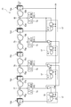
- the signal processing device 71 includes a timing error estimation unit 7a and a clock signal control unit 17 for the logic circuit 77, and a timing error estimation unit 7b and a clock signal control unit 17 for the logic circuit 78.
- a timing error estimation unit 7c and a clock signal control unit 17 are provided for the logic circuit 79, and a timing error estimation unit 7d and a clock signal control unit 17 are provided for the logic circuit 80.
- the timing error estimation units 7a, 7b, 7c, 7d and the clock signal control unit 17 have the same configuration as the timing error estimation unit 7 and the clock signal control unit 17 shown in FIG. Then, the explanation is omitted.
- timing error estimation unit 7a is provided for checkpoints C1, C2, C3, and C4 of each logic circuit 77, 78, 79, and 80.
- 7b, 7c, 7d are described, but this is only an example, and two or three other logic circuits are provided, and each checkpoint (in the middle of processing) of the logic circuit is provided.
- a timing error estimation unit may be provided.
- the timing error estimation unit 7a is connected to the check point C1 in the middle of processing between the first logic block 77a and the second logic block 77b, as in FIG.
- the timing error estimation unit 7a extracts the data processed in the first logic block 77a from the logic circuit 77 via the checkpoint C1, and at that time, the arithmetic processing of the first logic block 77a is performed as a clock signal. It can be determined whether or not the end of the first half of CK is completed before the falling edge (during the rising period).
- Each timing error estimation unit 7a, 7b, 7c, 7d determines whether the timing of the data has already shifted from the clock signal CK in the middle of processing in the corresponding logic circuit 77, 78, 79, 80, respectively. However, if the timing is shifted, it can be assumed that the arithmetic processing cannot be completed within the time assumed by the corresponding logic circuits 77, 78, 79, 80. In this way, each timing error estimation unit 7a, 7b, 7c, 7d is in the middle of arithmetic processing in the corresponding logic circuit 77, 78, 79, 80. It can be estimated whether or not it is operating.
- the signal processing device 71 includes a timing error estimation unit 7a and a clock signal control unit 17, a timing error estimation unit 7b and a clock signal control unit 17, a timing error estimation unit 7c and a clock signal control unit 17.
- OR circuits 75a, 75b, and 75c are provided as signal integration determination units, for example, the output unit of the timing error estimation unit 7a is connected to the input unit of the clock signal control unit 17 via the OR circuit 75a. It is connected.
- the OR circuit 75a is connected to the output unit of the timing error estimation unit 7a at one input unit and to the other input unit is connected to the output unit of the OR circuit 75b as a signal integration determination unit at the subsequent stage. Therefore, the logical sum of the data from the timing error estimation unit 7a and the data from the subsequent OR circuit 75b can be obtained.
- the OR circuit 75a receives the estimated timing error signal STE_1 from the timing error estimating unit 7a, receives the estimated timing error signal STE (not shown) output from the subsequent OR circuit 75b, or In both cases, an estimated timing error signal STE can be generated and sent to the latch circuit 19 of the clock signal control unit 17.
- the latch circuit 19 When the latch circuit 19 receives the estimated timing error signal STE from the corresponding OR circuit 75a, the latch circuit 19 generates the gating clock signal GCK gated with the clock signal CK, as in the first embodiment described above, This is sent to the flip-flop 72a connected to the output unit. As a result, the flip-flop 72a can execute the processing operation at the correct timing in synchronization with the new rising period of the gating clock signal GCK.
- “ ⁇ ” indicating the negation provided in the input part of the AND circuit 20 in FIG. 1 is provided in the output part of the latch circuit 19, but as in FIG. You may provide in an input part.
- the OR circuit 75b in the subsequent stage of the OR circuit 75a also receives the estimated timing error signal STE_2 from the timing error estimation unit 7b or outputs the estimated timing error signal STE (not shown) output from the subsequent OR circuit 75c.
- the estimated timing error signal STE is generated, and this is generated by the latch circuit 19 of the clock signal control unit 17 (in FIG. 12, the configuration of the clock signal control unit 17 is the same). The numbering is omitted.
- the gating clock signal GCK gated with the clock signal CK is generated as in the first embodiment described above. This is sent to the flip-flop 72b connected to the output unit. As a result, the flip-flop 72b can execute the processing operation at the correct timing in synchronization with the new rising period of the gating clock signal GCK.
- the OR circuit 75a in the preceding stage of the OR circuit 75b also sends the gating clock signal GCK to the latch circuit 19 based on the estimated timing error signal STE received from the succeeding OR circuit 75b as described above. Can be generated. As a result, not only the subsequent flip-flop 72b but also the previous flip-flop 72a can execute the processing operation at the correct timing in synchronization with the new rising period of the gating clock signal GCK.
- the OR circuit 75c in the subsequent stage of the OR circuit 75b also receives the estimated timing error signal STE_3 from the timing error estimating unit 7c or receives the estimated timing error signal STE_4 output from the subsequent timing error estimating unit 7d. In both cases, the estimated timing error signal STE can be generated and sent to the latch circuit 19 of the clock signal controller 17.
- a logic that is a signal integration determination unit is provided between the last timing error estimation unit 7d and the clock signal control unit 17. The summing circuit is not provided, and the estimated timing error signal STE_4 generated by the last timing error estimating unit 7d can be sent to the clock signal control unit 17 and the preceding OR circuit 75c as it is.
- all the OR circuits 75a, 75b, and 75c preceding the last timing error estimating unit 7d are estimated based on the estimated timing error signal STE_4 generated by the last timing error estimating unit 7d.
- the timing error signal STE is generated, and the gating clock signal GCK can be generated by each latch circuit 19 based on the estimated timing error signal STE.
- all the flip-flops 72a, 72b, 72c, 72d in the preceding stage of the logic circuit 80 having the timing error estimation unit 7d that generates the estimated timing error signal STE_4 are connected to the gating output from each clock signal control unit 17.
- the processing operation can be executed at the correct timing in synchronization with the new rising period of the clock signal GCK.
- the data is transferred to the clock signal CK in the middle of processing in the logic circuits 77, 78, 79, 80 by any one of the plurality of timing error estimation units 7a, 7b, 7c, 7d.
- the clock signal is supplied to the logic circuit (error estimation logic circuit) 79 whose timing is shifted and the logic circuits 77 and 78 in the previous stage of the logic circuit 79.
- OR circuits 75a, 75b, and 75c are provided as signal integration determination units to be controlled.
- the timing error estimation unit 7c only applies to all the logic circuits 77 and 78 preceding the logic circuit 79, including the logic circuit 79 estimated to be out of timing.
- the obtained estimation result of the timing error can be reflected, and the clock signal CK can be gated only by the minimum logic circuits 77, 78, 79 that may cause malfunction.
- the timing error estimation units 7a, 7b, 7c, 7d having the same configuration as the timing error estimation unit 7 shown in FIG. 1 are connected to the check points C1, C2 of the logic circuits 77, 78, 79, 80.
- the present invention is not limited to this, and the timing error estimation unit having the same configuration as the timing error estimation unit 37 shown in FIG. , 79, 80 may be signal processing devices connected to checkpoints C1, C2, C3, C4.
- a signal processing device 81 including a plurality of timing error estimation units 37a, 37b, 37c, and 37d is shown. This signal processing device 81 is more specifically shown, and a common wiring is provided for the plurality of timing error estimation units 37a, 37b, 37c, and 37d, and the clock signal CK is transmitted to each timing error estimation unit by the wiring. It is good also as a structure which can be supplied to 37a, 37b, 37c, 37d.
- timing error estimation units 7, 37, 37a, 37b, 37c, and 37d, the clock signal control unit 17, the signal integration determination units 60 and 65, the OR circuit (signal integration determination) Part) 75a, 75b, 75c, 75d, the first delay unit 46, the second delay unit 47, the third delay unit 48 has been described for the configuration as described above, the present invention is not limited to this,
- various timing error estimation units that combine various transistors, logic circuits, etc., clock signal control units, signal integration determination units, first delay units, second delay units, and third delay units may be applied. .
- the signal processing device has been described in which one checkpoint is provided between the sending-side and receiving-side flip-flops, and the timing error estimation unit is provided at the checkpoint.
- a signal processing apparatus may be provided in which a plurality of checkpoints are provided between the flip-flops on the sending side and the receiving side, and a timing error estimation unit is provided at each checkpoint.
- each timing error estimation unit between the sending side and receiving side flip-flops using the signal integration determining unit 60 shown in FIG. 11A or the signal integration determining unit 65 shown in FIG. 11B. Based on the estimated timing error signal obtained from the above, one estimated timing error signal STE can be generated, and the same effect as in the above-described embodiment can be obtained.
Landscapes
- Physics & Mathematics (AREA)
- Engineering & Computer Science (AREA)
- Theoretical Computer Science (AREA)
- Nonlinear Science (AREA)
- General Engineering & Computer Science (AREA)
- General Physics & Mathematics (AREA)
- Manipulation Of Pulses (AREA)
Abstract
論理回路における最終的な処理結果を事後的に解析することなく、論理回路の処理の途中段階で、論理回路が正しいタイミングで動作しているか否かを推測できる信号処理装置および信号処理方法を提案する。信号処理装置(1)では、乗算器(4)において処理途中の段階でデータ(D)がクロック信号(CK)に対して既にタイミングがずれていれば、乗算器(4)が想定した時間(この場合、1クロックの周期12[ns])内に演算処理が終了し得ないと推測でき、かくして乗算器(4)における最終的な演算処理結果を事後的に解析することなく、乗算器(4)の演算処理の途中段階で、乗算器(4)が正しいタイミングで動作しているか否かを推測できる。
Description
本発明は信号処理装置および信号処理方法に関する。
例えば、送り側のフリップフロップと受け側のフリップフロップとの間に演算回路が設けられた信号処理装置としては、送り側のフリップフロップから出力されたデータを演算回路にて演算処理した後、受け側のフリップフロップに受け渡す動作が、クロック信号に同期して行われる同期式が知られている。
このような信号処理装置は、クロック信号の立ち上がりに合わせてフリップフロップが動作し得るように設計されており、クロック信号の立ち上がりエッジ後から次の立ち上がりエッジ前までの1周期の間に、送り側のフリップフロップから演算回路を経由して受け側のフリップフロップにデータが受け渡される。
例えばフリップフロップ間に設けられた演算回路におけるクリティカルパスの処理時間が12[ns]である場合には、クロック信号の立ち上がりエッジ後から次の立ち上がりエッジ前までの1クロックの周期が12[ns]以上あれば、送り側のフリップフロップから演算回路を経由して送られたデータを受け側のフリップフロップにて受け取ることができ、演算回路や受け側のフリップフロップにて誤作動が生じることなく、正常な動作を行え得る。
しかしながら、このような信号処理装置でも、演算回路での処理時間が経年劣化等によって長くなってしまう虞もある。この場合、受け側のフリップフロップでは、送り側のフリップフロップから演算回路を経由して送られたデータを受け取るタイミングがクロック信号の立ち上がり時からずれ、その結果、誤ったデータを受け取ってしまい、誤作動が発生してしまう虞がある。
そこで、従来、クロック信号に同期して送り側のフリップフロップから演算回路を経由し受け側のフリップフロップに到達したデータと、これとは別に、クロック信号のクロック周期とは異なるクロック周期に同期させ送り側のフリップフロップから演算回路を経由し受け側のフリップフロップに到達したデータとを比較し、これら2つのデータが不一致のとき、演算回路にてデータの処理時間が長くなりタイミングエラーが生じていると判断するタイミングエラー検出回路が考えられている(例えば、非特許文献1参照)。
D.Ernst,N.Kim,S.Das,S.Pant,R.Rao,T.Pham,C.Ziesler,D.Blaauw,T.Austin,K.Flautner,and T.Mudge,"Razor:A Low-Power Pipeline Based on Circuit-Level Timing Speculation,"in Proc.IEEE/ACM Intl.Symp.Microarchitecture,pp.7-18,Dec.2003.
しかしながら、かかる構成でなるタイミングエラー検出回路では、演算回路でのタイミングエラーを事後的に検出しているため、演算回路にてタイミングエラーが生じている誤ったデータにて既に他の回路でもデータ処理が行われており、各回路でのデータ訂正を行うことが困難となる。そのため、各回路でのデータ訂正の手間を考えると、従来のように演算回路における最終的な演算処理結果を事後的に解析するのでなく、演算回路の演算処理の途中段階で演算回路が正しいタイミングで動作しているか否かを推測できることが好ましい。
そこで、本発明は以上の点を考慮してなされたもので、論理回路における最終的な処理結果を事後的に解析することなく、論理回路の処理の途中段階で、論理回路が正しいタイミングで動作しているか否かを推測できる信号処理装置および信号処理方法を提案することを目的とする。
本発明の請求項1における信号処理装置および請求項9の信号処理方法では、所定のクロック信号に同期させ所定のタイミングでデータを処理して出力する論理回路から処理途中のデータを取得し、処理途中の段階で該データが前記クロック信号に対してタイミングがずれているか否かを判断することを特徴とする。
本発明によれば、論理回路において処理途中の段階でデータがクロック信号に対して既にタイミングがずれていれば、論理回路が想定した時間内に処理が終了し得ないと推測でき、かくして論理回路における最終的な処理結果を事後的に解析することなく、論理回路の処理の途中段階で、論理回路が正しいタイミングで動作しているか否かを推測できる。
以下図面に基づいて本発明の実施の形態を詳述する。
(1)第1の実施の形態
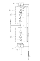
図1において、1は本発明の信号処理装置を示し、例えば、送り側のフリップフロップ2と受け側のフリップフロップ3との間に、論理回路として乗算器4が配置されており、クロック信号CKに同期して送り側フリップフロップ2から出力されたデータDが乗算器4にて乗算された後、受け側のフリップフロップ3に出力され得る。この実施の形態の場合、乗算器4は、複数の論理ゲートから構成された第1論理ブロック5aおよび第2論理ブロック5bからなり、クロック信号CKに同期して第1論理ブロック5aで演算処理されたデータDを第2論理ブロック5bで演算処理することで乗算したデータを得る。
図1において、1は本発明の信号処理装置を示し、例えば、送り側のフリップフロップ2と受け側のフリップフロップ3との間に、論理回路として乗算器4が配置されており、クロック信号CKに同期して送り側フリップフロップ2から出力されたデータDが乗算器4にて乗算された後、受け側のフリップフロップ3に出力され得る。この実施の形態の場合、乗算器4は、複数の論理ゲートから構成された第1論理ブロック5aおよび第2論理ブロック5bからなり、クロック信号CKに同期して第1論理ブロック5aで演算処理されたデータDを第2論理ブロック5bで演算処理することで乗算したデータを得る。
これに加えて、乗算器4は、第1論理ブロック5aと第2論理ブロック5bとの間にタイミングエラー推測部7が接続されたチェックポイントCがあり、第1論理ブロック5aにて処理されたデータDをタイミングエラー推測部7に送出し得る。ここで、この実施の形態の場合、乗算器4は、最も長い処理経路であるクリティカルパスでの処理時間が、クロック信号CKの1クロックの周期(例えば12[ns])と同じになっている。
また、乗算器4は、第1論理ブロック5aでの処理時間が1クロックの前半の立ち上がり期間H1(立ち上がりエッジから立ち下がりエッジまでの期間であり、ここでは6[ns])に設定されているとともに、第2論理ブロック5bの処理時間が1クロックの後半の立ち下がり期間L1(立ち下がりエッジから立ち上がりエッジまでの期間であり、ここでは6[ns])に設定されている。なお、クロック信号CKは、立ち上がり期間H1と立ち下がり期間L1とを順次交互に繰り返し、デューティ比が50%の立ち上がり期間H1および立ち下がり期間L1とで1クロックを構成している。
この実施の形態の場合、乗算器4は、上述したように第1論理ブロック5aおよび第2論理ブロック5bの演算処理がクロック信号CKに同期しており、データDがクリティカルパスを経由する際でも1クロックの周期内に終了していなければならず、それゆえ、第1論理ブロック5aの演算処理がクロック信号CKの前半部分末端の立ち下がりエッジ前まで(立ち上がり期間H1中)に終了していなければならない。
そこで、タイミングエラー推測部7は、第1論理ブロック5aで処理されたデータDを、中間点であるチェックポイントCを介して乗算器4から抽出し、その時点で、第1論理ブロック5aの演算処理がクロック信号CKの前半部分末端の立ち下がりエッジ前まで(立ち上がり期間H1中)に終了しているか否かを判断する。その結果、タイミングエラー推測部7は、第1論理ブロック5aの演算処理がクロック信号CKの立ち下がりエッジ後に行われた場合、第1論理ブロック5aおよび第2論理ブロック5bを合わせた演算処理が1クロックの周期内では終了しないと判断し、乗算器4にてタイミングエラーが発生すると推測し得る。
ここで、タイミングエラー推測部7は、チェックポイントCにおけるデータDの遷移を検出する遷移検出部8と、遷移検出部8にて検出されたデータDの遷移がクロック信号CKの立ち下がり期間L1中であるか否かを判断するエラー判断部9とから構成されている。実際上、遷移検出部8は、否定排他論理和回路12を有しており、チェックポイントCで得られた乗算器4の処理途中のデータDを、遅延回路11a,11bを経由して否定排他論理和回路12の一方の入力部に入力するとともに、チェックポイントCで得られた乗算器4の処理途中のデータDを否定排他論理和回路12の他方の入力部にそのまま入力し得る。
否定排他論理和回路12は、一方の入力部から入力された遅延データと、他方の入力部から入力されたデータDの否定排他論理和をとり、その結果得られるデータをエラー判断部9に出力する。例えば、否定排他論理和回路12は、遅延データおよびデータDがともに立ち下がっているとき、および、ともに立ち上がっているとき、データDが遷移していないことを示す「1」データを出力部からエラー判断部9に出力し得る。
一方、チェックポイントCにて立ち下がっていたデータDが立ち上がったり、或いは立ち上がっていたデータDが立ち下がったりデータDの遷移が生じると、否定排他論理和回路12は、遷移前の遅延データが一方の入力部に入力されるとともに、遷移後のデータDがそのまま他方の入力部に入力され、遅延データとデータDの否定排他論理和をとり、データDが遷移したことを示す「0」データを出力部からエラー判断部9に出力し得る。
ここで、エラー判断部9は、一方の入力部が否定排他論理和回路12の出力部と接続された論理積回路14と、一方の入力部に論理積回路14の出力部が接続されているとともに、他方の入力部にクロック信号CKが入力され、出力部が論理積回路14の他方の入力部に接続された否定論理和回路15とを有する。この場合、論理積回路14は、否定排他論理和回路12の出力部よりデータDが遷移したことを示す「0」データが一方の入力部に入力されると、出力部から「0」データを出力し得る。
否定論理和回路15は、他方の入力部にクロック信号CKが入力されており、一方の入力部から入力された論理積回路14からの「0」データが、クロック信号CKの立ち上がり期間H1、または立ち下がり期間L1のいずれのタイミングで得られたかを判断し得る。例えば、否定論理和回路15は、一方の入力部に論理積回路14から「0」データが入力されたとき、立ち下がり期間L1のクロック信号CKが他方の入力部に入力されている場合、第1論理ブロック5aにおいてデータDの処理が、1クロックの前半部分末端の立ち下がりエッジ前に終了していないことになるため、乗算器4によるデータDの処理がこのままだと1クロック内で処理できずタイミングエラーが発生する虞があることを示す推測タイミングエラー信号STE(この場合、「1」データ)を、出力部から出力し得る。
因みに、エラー判断部9は、否定論理和回路15の出力部からタイミングエラーを推測した推測タイミングエラー信号STEが出力されると、当該推測タイミングエラー信号STEが論理積回路14の他方の入力部に入力されるものの、論理積回路14の一方の入力部に「0」データが入力されている限り論理積回路14の出力部からは「0」データが出力され続ける。
一方、否定論理和回路15は、一方の入力部に論理積回路14からの「0」データが入力されたとき、立ち上がり期間H1のクロック信号CKが他方の入力部に入力されている場合、第1論理ブロック5aにおいてデータDの処理が、1クロックの前半部分末端の立ち下がりエッジ前に終了したことになるため、乗算器4によるデータDの処理が1クロック内で処理できるであろうことを示す「0」データを出力部から出力し得る。
因みに、エラー判断部9は、遷移検出部8よりデータDが遷移していないことを示す「1」データが論理積回路14の一方の入力部に入力されると、否定論理和回路15の出力部からはクロック信号CKの立ち上がり、立ち下がりにかかわらず「0」データが出力される。
かかる構成に加えて、本発明の信号処理装置1には、タイミングエラー推測部7から出力された「1」データに基づいてクロック信号CKをゲーティングするクロック信号制御部17がタイミングエラー推測部7の出力に接続されている。実際上、クロック信号制御部17は、ラッチ回路19と論理積回路20とで構成され、タイミングエラー推測部7から出力された例えば推測タイミングエラー信号STEがラッチ回路19に入力され得る。
ラッチ回路19は、クロック信号CKの立ち上がり立ち下がりが反転した反転クロック信号が入力されており、クロック信号CKにおける1クロックの周期を検出可能に構成されている。また、ラッチ回路19は、出力部に論理積回路20が接続されており一度、タイミングエラー推測部7から推測タイミングエラー信号STE(「1」データ)を受け取ると、クロック信号CKにおいて次の立ち上がりエッジが供給されても、論理積回路20に対して「1」データをそのまま出力し続け得る。
論理積回路20は、一方の入力部にクロック信号CKが入力されているとともに、他方の入力部にラッチ回路19からのデータが入力され、これらクロック信号CKと、ラッチ回路19からのデータの論理積をとり、その結果得られたゲーティングクロック信号GCKを送り側のフリップフロップ2および受け側のフリップフロップ3に出力し得る。これにより送り側のフリップフロップ2および受け側のフリップフロップ3は、クロック信号制御部17から受け取ったゲーティングクロック信号GCKに同期して動作し得る。
この場合、論理積回路20は、ラッチ回路19から出力された「1」データを反転させた「0」データが他方の入力部に入力されている限り、クロック信号CKが立ち上がってもそのまま「0」データを出力し続け、送り側のフリップフロップ2および受け側のフリップフロップ3に対して、クロック信号CKをゲーティングし、次の立ち上がりエッジが発生することなく立ち下がり状態がそのまま維持されたゲーティングクロック信号GCKを出力し得る。
ラッチ回路19は、その後、タイミングエラー推測部7から「0」データを受け取り、ゲーティングした1クロックの次の1クロックの立ち上がりエッジが発生したクロック信号CKが入力されると、「0」データを論理積回路20に出力し得る。これにより論理積回路20は、ラッチ回路19に接続された他方の入力部に「0」データが反転した「1」データが入力されるとともに、一方の入力部に立ち上がったクロック信号CKが入力され、これら両者の論理積をとることでゲーティングクロック信号GCKを立ち上げ、これを送り側のフリップフロップ2および受け側のフリップフロップ3に出力し得る。
これにより送り側のフリップフロップ2および受け側のフリップフロップ3は、タイミングエラー推測部7にて推測タイミングエラー信号STEが生成されなくなると、ゲーティングされて立ち上がらなかった1クロックの立ち上がり期間H1の次の1クロックの立ち上がり期間H1が、ゲーティングクロック信号GCKに基づいて供給され、周期が2倍(24[ns])となった1クロックに同期して処理動作を実行し得る。かくして、乗算器4では、クロック信号CK(ゲーティングクロック信号GCK)の新たな立ち上がり期間H1に同期して正しいタイミングで動作を行え、正しいデータDを受け側のフリップフロップ3に出力し、さらには受け側のフリップフロップ3においてもタイミングエラーによる誤ったデータにより動作することを防止し得る。
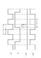
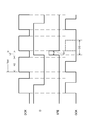
次に、このようなタイミングエラー推測訂正処理について、図2に示すタイミングチャートを用いて簡単に説明する。図2に示すように、クロック信号CKは、立ち上がり期間H1と立ち下がり期間L1を順次交互に繰り返すパルス状の信号である。前半にある立ち上がり期間H1と、後半にある立ち下がり期間L1とで1クロックの周期Tck1が構成されている。
ここで、図2では、第1論理ブロック5aにおける演算処理が想定以上の時間を要し、第1論理ブロック5aの演算処理がクロック信号CKの前半部分末端の立ち下がりエッジ前まで(立ち上がり期間H1中)に終了していないデータDを示しており、その結果、タイミングエラー推測部7において、クロック信号CKの立ち下がり期間L1中にデータDの遷移が検出される。
この場合、推測タイミングエラー信号STEは、クロック信号CKが立ち上がることでリセットされ、その結果、遷移検出部8にて検出したデータDの遷移時点からクロック信号CKの立ち上がりエッジまでの時間Errの間に発生し得る。クロック信号制御部17にて生成されるゲーティングクロック信号GCKは、推測タイミングエラー信号STEの発生後から次の1クロックの立ち上がり期間H1までの間(図2中「CG」と表記)、クロック信号CKをゲーティングし、推測タイミングエラー信号STE生成直後の立ち上がり期間H1を生成することなく、そのまま立ち下がり期間L1を維持し得る。
因みに、図3は、推測タイミングエラー信号STEが連続して発生したときのスパイスシミュレーションの結果を示すタイミングチャートである。クロック信号CKの連続する立ち下がり期間中にそれぞれデータDの遷移があり、推測タイミングエラー信号STEがそれに応じて連続して発生している。この場合、初めの推測タイミングエラー信号STEの発生からその直後のクロック信号CKの立ち下がりエッジまで、クロック信号CKがゲーティングされた後、続けて、推測タイミングエラー信号STEの発生からその直後のクロック信号CKの立ち下がりエッジまで、再びクロック信号CKがゲーティングされたゲーティングクロック信号GCKが生成されている。
このように、信号処理装置1では、推測タイミングエラー信号STEが検出されなくなるまで推測タイミングエラー信号STEの発生からその直後のクロック信号CKの立ち下がりエッジまでクロック信号CKをゲーティングし、乗算器4においてクロック信号CK(ゲーティングクロック信号GCK)の立ち上がり期間H1に同期した正常な動作を確実に行わせ得るようになされている。
以上の構成において、信号処理装置1では、所定のクロック信号CKに同期させ所定のタイミングでデータDを処理して出力する乗算器4から処理途中のデータDを取得し、処理途中の段階で当該データDがクロック信号CKに対してタイミングがずれているか否かを判断するタイミングエラー推測部7を設けるようにした。
信号処理装置1では、乗算器4において処理途中の段階でデータDがクロック信号CKに対して既にタイミングがずれていれば、乗算器4が想定した時間(この場合、1クロックの周期12[ns])内に演算処理が終了し得ないと推測でき、かくして乗算器4における最終的な演算処理結果を事後的に解析することなく、乗算器4の演算処理の途中段階で、乗算器4が正しいタイミングで動作しているか否かを推測できる。
また、信号処理装置1では、タイミングエラー推測部7にて乗算器4においてデータDがクロック信号CKに対しタイミングがずれていると推測したとき、クロック信号制御部17によって、乗算器4に対するクロック信号CKをゲーティングし、乗算器4に対するクロック信号CKの供給を制御するようにした。このように、信号処理装置1では、タイミングエラー推測部7にて得られたタイミングエラー発生の推測結果を反映させ、乗算器4に対するクロック信号CKをゲーティングすることができ、これにより、受け側のフリップフロップ3がタイミングエラーの生じた誤ったデータにより動作することを防止し得る。
(2)シミュレーション試験
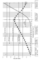
次に、図1に示すような信号処理装置1を用意し、タイミングエラーの推測と、タイミングエラー時のクロック信号CKのゲーティングについてシミュレーション試験を行った。このシミュレーション試験では、VDD1.8[V]、25[C]で乗算器4を用い、乗算器4の216のランダムな入力ベクトル使用して動作させた。そして、クロック信号CKのサイクル時間を小さくしてゆき(すなわち、クロック信号CKの1クロックの周期を短くしてゆき)、乗算器4にて乗算に必要な1クロックのサイクル数と、乗算器4のスループットとを調べたところ、図4に示すような結果が得られた。
次に、図1に示すような信号処理装置1を用意し、タイミングエラーの推測と、タイミングエラー時のクロック信号CKのゲーティングについてシミュレーション試験を行った。このシミュレーション試験では、VDD1.8[V]、25[C]で乗算器4を用い、乗算器4の216のランダムな入力ベクトル使用して動作させた。そして、クロック信号CKのサイクル時間を小さくしてゆき(すなわち、クロック信号CKの1クロックの周期を短くしてゆき)、乗算器4にて乗算に必要な1クロックのサイクル数と、乗算器4のスループットとを調べたところ、図4に示すような結果が得られた。
図4では、乗算器4にて乗算に必要なクロック信号CKのサイクル数を△で表記し、スループットを■で表記した。図4から、クロック信号CKのサイクル時間8.2[ns]まではスループットが向上した。また、クロック信号CKのサイクル時間9[ns]よりも小さくしてゆくと、クロック信号制御部17によるクロック信号CKのゲーティングによってサイクル数が次第に増えてゆき、それに伴いスループットが低下してゆくことが確認できた。ただし、クロック信号CKのサイクル時間が6.4[ns]では、スループットは向上しないものの、クロック信号CKのサイクル時間10.8[ns]と同様のスループットが得られ、正常に動作することが確認できた。
(3)第2の実施の形態
図1との対応部分に同一符号を付して示す図5において、31は第2の実施の形態による信号処理装置を示し、第1の実施の形態とは、乗算器34から処理途中のデータを抽出するチェックポイントCの位置が異なっている。この場合、乗算器34は、最も長い処理経路であるクリティカルパスでの処理時間が、クロック信号CKの1クロック(例えば12[ns])に調整されている。ただし、第2の実施の形態における乗算器34は、第1論理ブロック35aでの処理時間が1クロックの周期2/3である8[ns]に設定され、第2論理ブロック35bの処理時間が1クロックの周期1/3である4[ns]に設定されている。
図1との対応部分に同一符号を付して示す図5において、31は第2の実施の形態による信号処理装置を示し、第1の実施の形態とは、乗算器34から処理途中のデータを抽出するチェックポイントCの位置が異なっている。この場合、乗算器34は、最も長い処理経路であるクリティカルパスでの処理時間が、クロック信号CKの1クロック(例えば12[ns])に調整されている。ただし、第2の実施の形態における乗算器34は、第1論理ブロック35aでの処理時間が1クロックの周期2/3である8[ns]に設定され、第2論理ブロック35bの処理時間が1クロックの周期1/3である4[ns]に設定されている。
よって、この実施の形態の場合、タイミングエラー推測部37は、チェックポイントCから得られたデータDに基づいて、第1論理ブロック35aによるデータDの処理が8[ns]以内に終了しているか否かを判断し、その結果、第1論理ブロック35aによるデータDの処理が8[ns]を越えているときタイミングエラーが発生していると推測し得る。
この場合、タイミングエラー推測部37は、エラー判断部39に検出用クロック信号生成回路40を備えている点で、上述した第1の実施の形態とは相違しており、当該検出用クロック信号生成回路40によってチェックポイントCにてタイミングエラーを推測可能な検出用クロック信号DCKを生成し得るようになされている。
実際上、エラー判断部39は、検出用クロック信号生成回路40の出力が否定論理和回路15の他方の入力部に接続された構成を有し、検出用クロック信号生成回路40により生成された検出用クロック信号DCKと、論理積回路14からのデータの否定論理和をとり、その結果得られたデータをクロック信号制御部17に出力し得る。
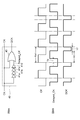
ここで、図6Aに示すように、検出用クロック信号生成回路40は、一方の入力部にクロック信号CKが入力され、他方の入力部に遅延回路41a,41b,41c,41dを介して遅延クロック信号Delayed_CKが入力される論理和回路43が設けられている。この場合、遅延回路41a,41b,41c,41dによるクロック信号CKの遅延量は、チェックポイントCの位置に応じて選定されている。
この実施の形態の場合、図6Bに示すように、クロック信号CKは、立ち上がり期間および立ち下がり期間がともに6[ns]であることから、遅延回路41a,41b,41c,41dは、クロック信号CKを遅延させる遅延量Tdとして2[ns]が選定されており、クロック信号CKを2[ns]遅延させた遅延クロック信号Delayed_CKを生成する。これにより論理和回路43は、クロック信号CKと遅延クロック信号Delayed_CKの論理和をとることで、第1論理ブロック35aの処理時間と同じ8[ns]の立ち上がり期間H2の検出用クロック信号DCKを生成し、これを否定論理和回路15に出力し得る。
これにより、否定論理和回路15は、検出用クロック信号DCKの立ち下がり期間L2中にデータDの立ち下がり、または立ち上がりの遷移があったとき、第1論理ブロック35aでの処理が想定していた時間(この場合、8[ns])以上かかりタイミングエラーが発生しているとして、推測タイミングエラー信号STEをクロック信号制御部17に出力し得る。
一方、検出用クロック信号DCKの立ち下がり期間L2中にデータDの遷移が発生しなかった場合には、第1論理ブロック35aでの処理が検出用クロック信号DCKの立ち下がりエッジ前に終了しており、タイミングエラーが発生しないことを示す「0」データをクロック信号制御部17に出力し得る。
なお、クロック信号制御部17は、上述した第1の実施の形態と同様の構成を有しており、タイミングエラー推測部37から推測タイミングエラー信号を受け取ると、上述した第1の実施の形態と同様に、クロック信号CKをゲーティングしたゲーティングクロック信号GCKを生成し、これを送り側のフリップフロップ2および受け側のフリップフロップ3へ出力し得る。
これにより送り側のフリップフロップ2および受け側のフリップフロップ3は、タイミングエラー推測部37にて推測タイミングエラー信号STEが生成されなくなると、ゲーティングクロック信号GCKに基づいて、新たな1クロックが発生し、1クロックの立ち上がりに同期して処理動作を実行し得る。かくして、乗算器34では、クロック信号CK(ゲーティングクロック信号GCK)の立ち上がり期間に同期した正常な動作を行え、正しいデータDを受け側のフリップフロップ3に出力し、さらには受け側のフリップフロップ3においても誤ったデータによる誤作動を防止し得る。
ここで、このようなタイミングエラー推測訂正処理について、図7に示すタイミングチャートを用いて簡単に説明する。図7に示すように、検出用クロック信号DCKは、立ち上がり期間H2と立ち下がり期間L2とが第1論理ブロック35aの処理時間と第2論理ブロック35bの処理時間とにそれぞれ調整されている。図7では、第1論理ブロック35aにおける演算処理が想定以上の時間を要し、第1論理ブロック35aの演算処理が検出用クロック信号DCKの立ち下がりエッジ前(8[ns]以内)に終了していないデータDを示しており、その結果、タイミングエラー推測部37において、検出用クロック信号DCKの立ち下がり期間L2中にデータDの遷移が検出される。
この場合、推測タイミングエラー信号STEは、検出用クロック信号DCKが立ち上がることでリセットされ、その結果、遷移検出部8にて検出したデータDの遷移時点から検出用クロック信号DCKの立ち上がりエッジまでの時間Errの間に発生し得る。クロック信号制御部17にて生成されるゲーティングクロック信号GCKは、推測タイミングエラー信号STEの発生後から次の1クロックの立ち上がり期間H2までの間(図7中「CG」と表記)、クロック信号CKをゲーティングし、推測タイミングエラー信号STE生成直後の立ち上がり期間H2を生成することなく、そのまま立ち下がり期間L2を維持し得る。
このように、信号処理装置31でも、推測タイミングエラー信号STEの発生からその直後のクロック信号CKの立ち下がりエッジまでクロック信号CKをゲーティングし、乗算器34においてクロック信号CKの立ち上がり期間H2に同期した正常な動作を確実に行わせ得るようになされている。
以上の構成において、信号処理装置31でも、上述した第1の実施の形態と同様に、乗算器34において処理途中の段階でデータDがクロック信号CKに対して既にタイミングがずれていれば、乗算器34が想定した時間内に演算処理が終了し得ないと推測でき、かくして乗算器34における最終的な演算処理結果を事後的に解析することなく、乗算器34の演算処理の途中段階で、乗算器34が正しいタイミングで動作しているか否かを推測できる。
また、この信号処理装置31では、乗算器34から処理途中のデータDを取得する任意の位置に対応して、クロック信号CKの立ち上がりおよび立ち下がりのデューティ比を可変した検出用クロック信号DCKを生成する検出用クロック信号生成回路40を設け、データDが検出用クロック信号DCKに対してタイミングがずれているか否かを判断するようにした。
これにより、信号処理装置31では、乗算器34の任意の位置から処理途中のデータDを取得しても、当該データDが検出用クロック信号DCKに対してタイミングがずれているか否かの判断に基づいて、任意の位置であってもデータDがその時点でクロック信号CKに対してタイミングがずれているか否かを判断できる。なお、このような検出用クロック信号生成回路としてはPLLやDLLを利用して構築してもよい。
(4)他の実施の形態
なお、本発明は、本実施の形態に限定されるものではなく、本発明の要旨の範囲内で種々の変形実施が可能であり、例えば、送り側のフリップフロップ2と受け側のフリップフロップ3との間に設けた論理回路として、乗算器4,34を適用した場合について述べたが、本発明はこれに限らず、加算器や比較器等その他種々の組み合わせ回路を適用してもよく、また順序回路等その他種々の論理回路を適用してもよい。
なお、本発明は、本実施の形態に限定されるものではなく、本発明の要旨の範囲内で種々の変形実施が可能であり、例えば、送り側のフリップフロップ2と受け側のフリップフロップ3との間に設けた論理回路として、乗算器4,34を適用した場合について述べたが、本発明はこれに限らず、加算器や比較器等その他種々の組み合わせ回路を適用してもよく、また順序回路等その他種々の論理回路を適用してもよい。
また、上述した実施の形態においては、論理回路のチェックポイントとして、図1では乗算器4における1クロックの周期1/2時点にチェックポイントCを設け、一方、図5では乗算器34における1クロックの周期2/3時点にチェックポイントCを設けるようにした場合について述べたが、本発明はこれに限らず、例えば乗算器における1クロックの周期1/3時点や、周期1/4時点等その他種々の位置にチェックポイントを設けてもよく、この場合、検出用クロック信号生成回路40によってそれぞれ1クロックの周期1/3時点や、周期1/4時点に立ち下がりエッジがあるデューティ比を可変した検出用クロック信号DCKを生成すればよい。なお、具体的な一例については下記「(4‐2)論理回路について」で後述する。また、乗算器(論理回路)に対して複数箇所にチェックポイントCを設けるようにしてもよい。これについても、具体的な一例については下記「(4‐3)他の実施の形態による信号処理装置の回路構成について」で後述する。
さらに、上述した実施の形態においては、データの立ち上がりから立ち下がり、または立ち下がりから立ち上がりの遷移を検出する遷移検出部として、否定排他論理和回路12等を用いた場合について述べたが、本発明はこれに限らず、種々の論理ゲートを組み合わせることにより、データの立ち上がりから立ち下がり、または立ち下がりから立ち上がりの遷移を検出する構成を実現してもよい。
さらに、上述した実施の形態においては、データの遷移をクロック信号の立ち下がり期間中に検出したとき、当該データがクロック信号に対しタイミングがずれていると推測するエラー判断部として、論理積回路14および否定論理和回路15等を用いた場合について述べたが、本発明はこれに限らず、種々の論理ゲートを組み合わせることにより、データの遷移をクロック信号の立ち下がり期間中に検出したとき、当該データがクロック信号に対しタイミングがずれていると推測する構成を実現してもよい。
(4‐1)他の実施の形態による検出用クロック信号生成回路について
上述した第2の実施の形態においては、検出用クロック信号生成回路として、乗算器34のチェックポイントCの位置に合わせて予めクロック信号CKの遅延量を設定しなければならない検出用クロック信号生成回路を適用した場合について述べたか、本発明はこれに限らず、論理回路のチェックポイントCの位置に合わせてクロック信号CKの遅延量を数種類のうちから自由に選定可能な検出用クロック信号生成回路を適用してもよい。
上述した第2の実施の形態においては、検出用クロック信号生成回路として、乗算器34のチェックポイントCの位置に合わせて予めクロック信号CKの遅延量を設定しなければならない検出用クロック信号生成回路を適用した場合について述べたか、本発明はこれに限らず、論理回路のチェックポイントCの位置に合わせてクロック信号CKの遅延量を数種類のうちから自由に選定可能な検出用クロック信号生成回路を適用してもよい。
図8において、45は、クロック信号CKの遅延量を数種類のうちから自由に選定可能な検出用クロック信号生成回路を示し、この検出用クロック信号生成回路45は、論理回路(例えば、図5に示す乗算器34)から処理途中のデータDを取得するチェックポイントCの位置に応じて、クロック信号CKの立ち上がりおよび立ち下がりのデューティ比が最適な検出用クロック信号DCKを選択的に生成し得るようになされている。実際上、検出用クロック信号生成回路45には、遅延部として、第1遅延部46、第2遅延部47、および第3遅延部48を備えており、このうち第1遅延部46にクロック信号CKが入力され得るようになされている。
この場合、第1遅延部46の出力部は、選択スイッチ回路50(図8中、MUXとも表記)に接続されているとともに、第2遅延部47の入力部に接続されている。また、第2遅延部47の出力部は、選択スイッチ回路50に接続されているとともに、第3遅延部48の入力部に接続されている。さらに、第3遅延部48の出力部は、選択スイッチ回路50にのみ接続されている。
これにより、検出用クロック信号生成回路45は、クロック信号CKが第1遅延部46を経由して選択スイッチ回路50まで到達する第1経路と、クロック信号CKが第1遅延部46および第2遅延部47を経由して選択スイッチ回路50まで到達する第2経路と、クロック信号CKが第1遅延部46、第2遅延部47、および第3遅延部48を経由して選択スイッチ回路50まで到達する第3経路とが形成され得る。なお、この実施の形態の場合、遅延部として、第1遅延部46、第2遅延部47、および第3遅延部48の3つを設け、クロック信号CKが選択スイッチ回路50に到達する経路として3種類の経路を設けるようにした場合について述べたが、本発明はこれに限らず、2つや4つ等その他複数の遅延部を設け、2つや4つ等その他複数の経路を設けるようにしてもよい。
実際上、この実施の形態の場合、第1遅延部46は、例えば遅延回路46a,46bを備えており、遅延回路46a,46b分だけクロック信号CKを遅延させて選択スイッチ回路50まで到達させ得る。第2遅延部47は、例えば遅延回路47a,47bを備えており、第1遅延部46(遅延回路46a,46b)分、遅延したクロック信号CKを、さらに遅延回路47a,47b分だけ遅延させて選択スイッチ回路50まで到達させ得る。
第3遅延部48は、例えば遅延回路48a,48b,48c,48dを備えており、第1遅延部46(遅延回路46a,46b)分および第2遅延部47(遅延回路47a,47b)分、遅延したクロック信号CKを、さらに遅延回路48a,48b,48c,48d分だけ遅延させて選択スイッチ回路50まで到達させ得る。
このように、検出用クロック信号生成回路45は、クロック信号CKが選択スイッチ回路50に到達するまでに第1遅延部46、第2遅延部47、および第3遅延部48を経由する経路を変えることで、遅延量の異なる複数の遅延クロック信号Delayed_CKを生成し得、各遅延クロック信号Delayed_CKをそれぞれ選択スイッチ回路50へ出力し得るようになされている。
ここで、選択スイッチ回路50は、図示しない制御部から選択信号が入力されると、各第1遅延部46、第2遅延部47、および第3遅延部48から受け取った遅延クロック信号Delayed_CKのうち、選択信号に基づいて任意に選択された遅延クロック信号Delayed_CKだけを出力部から出力し得るようになされている。
選択スイッチ回路50は、第1遅延部46、第2遅延部47、および第3遅延部48の出力部から出力された複数の遅延クロック信号Delayed_CKのうち、論理回路(例えば、図5の乗算器34)のチェックポイントCの位置に応じて選択信号SELにより選ばれた所定遅延量の遅延クロック信号Delayed_CKを論理和回路51に出力し得る。
論理和回路51は、クロック信号CKが一方の入力部に入力されるとともに、選択スイッチ回路50から他方の入力部に遅延クロック信号Delayed_CKが入力され、クロック信号CKおよび遅延クロック信号Delayed_CKの論理和をとることで、第1論理ブロック35a(図5)の処理時間と同じ立ち上がり期間の検出用クロック信号DCKを生成し得る。これにより、論理和回路51は、生成した検出用クロック信号DCKをエラー判断部39の否定論理和回路15(図5)に出力し得る。
以上の構成において、この検出用クロック信号生成回路45では、論理回路(乗算器34)に設けた後であっても、クロック信号CKが第1遅延部46、第2遅延部47、および第3遅延部48を通過する経路を変えることで、論理回路のチェックポイントCの位置に合わせてクロック信号CKの立ち上がりおよび立ち下がりのデューティ比を調整した最適な検出用クロック信号DCKを容易に生成できる。
(4‐2)論理回路について
なお、上述した実施の形態において、論理回路として、図1では、第1論理ブロック5aでの処理時間が1クロックの周期1/2(例えば6[ns])に設定され、第2論理ブロック5bの処理時間が1クロックの周期1/2(6[ns])に設定された乗算器4を適用し、図5では、第1論理ブロック35aでの処理時間が1クロックの周期2/3(例えば8[ns])に設定され、第2論理ブロック35bの処理時間が1クロックの周期1/3(4[ns])に設定された乗算器34を適用した場合について述べたが、上述したように本発明はこれに限らず、第1論理ブロックおよび第2論理ブロック間が種々の処理時間に区分けされた論理ブロックを適用してもよい。
なお、上述した実施の形態において、論理回路として、図1では、第1論理ブロック5aでの処理時間が1クロックの周期1/2(例えば6[ns])に設定され、第2論理ブロック5bの処理時間が1クロックの周期1/2(6[ns])に設定された乗算器4を適用し、図5では、第1論理ブロック35aでの処理時間が1クロックの周期2/3(例えば8[ns])に設定され、第2論理ブロック35bの処理時間が1クロックの周期1/3(4[ns])に設定された乗算器34を適用した場合について述べたが、上述したように本発明はこれに限らず、第1論理ブロックおよび第2論理ブロック間が種々の処理時間に区分けされた論理ブロックを適用してもよい。
例えば、他の論理回路として、図9に示すように、第1論理ブロック55aでの処理時間(立ち上がり期間H3)が1クロックの周期1/3(例えば4[ns])に設定され、第2論理ブロック55bの処理時間(立ち下がり期間L3)が1クロックの周期2/3(8[ns])に設定された乗算器54を適用してもよい。この場合、乗算器54には、第1論理ブロック55aおよび第2論理ブロック55b間にチェックポイントCがあり、当該チェックポイントCにタイミングエラー推測部37(図5)が接続され得る。
これによりタイミングエラー推測部37は、乗算器54のチェックポイントCから得られたデータDに基づいて、第1論理ブロック55aによるデータDの処理が4[ns]以内に終了しているか否かを判断し、その結果、第1論理ブロック55aによるデータDの処理が4[ns]を越えているときタイミングエラーが発生していると推測し得る。
(4‐3)他の実施の形態による信号処理装置の回路構成について
図10は、他の実施の形態による信号処理装置56の概略の回路構成を示しており、複数のチェックポイントC1,C2を設け、各チェックポイントC1,C2毎にタイミングエラー推測部7a,7bを設けた構成を示している。なお、図10では、タイミングエラー推測部7a,7bに接続されるクロック信号制御部について、図1および図5に示したクロック信号制御部17の構成と同じであるため省略している。
図10は、他の実施の形態による信号処理装置56の概略の回路構成を示しており、複数のチェックポイントC1,C2を設け、各チェックポイントC1,C2毎にタイミングエラー推測部7a,7bを設けた構成を示している。なお、図10では、タイミングエラー推測部7a,7bに接続されるクロック信号制御部について、図1および図5に示したクロック信号制御部17の構成と同じであるため省略している。
そして、複数のチェックポイントC1,C2を設けた信号処理装置56でも、各タイミングエラー推測部7a,7b毎に、それぞれクロック信号CKに同期して所定のタイミングでデータDを処理する論理回路58,59から処理途中のデータDを取得し、処理途中の段階で当該データDがクロック信号CKに対してタイミングがずれているか否かを判断し得る。
例えば、図10に示す信号処理装置56では、送り側のフリップフロップ57aと、中間にあるフリップフロップ57bと、受け側のフリップフロップ57cとが設けられており、送り側のフリップフロップ57aおよび中間にあるフリップフロップ57b間に論理回路58が配置されているとともに、中間にあるフリップフロップ57bおよび受け側のフリップフロップ57c間に論理回路59が配置された構成を有している。
なお、一方の論理回路58には、第1論理ブロック58aおよび第2論理ブロック58b間にチェックポイントC1があり、当該チェックポイントC1にタイミングエラー推測部7aが接続され、他方の論理回路59にも、第1論理ブロック59aおよび第2論理ブロック59b間にチェックポイントC2があり、当該チェックポイントC2に別のタイミングエラー推測部7bが接続されている。
これにより、各タイミングエラー推測部7a,7bは、接続された論理回路58,59のチェックポイントC1,C2から得られたデータDに基づいて、それぞれ第1論理ブロック58a,59aによるデータDの処理が処理時間内に終了しているか否かを判断し、その結果、第1論理ブロック58a,59aによるデータDの処理が処理時間を越えているときタイミングエラーが発生していると推測し得る。
このような信号処理装置56では、例えばこれら論理回路58,59によりデータDを順番に処理し得るようになされており、その過程において、一方のタイミングエラー推測部7aから得られた推測タイミングエラー信号STE_1と、他方のタイミングエラー推測部7bから得られた推測タイミングエラー信号STE_2とが得られたとき、これら推測タイミングエラー信号STE_1,STE_2を基にクロック信号制御部(図示せず)を制御し、論理回路58,59を正しいタイミングで動作させ得る。次に、このような複数の推測タイミングエラー信号STE_1,STE_2が得られたときの各種動作について詳細に説明する。
(4‐3‐1)信号統合判定部について
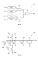
ここで、図11Aに示すように複数のタイミングエラー推測部7a,7b,…,7k-1,7kを設けた場合には、各タイミングエラー推測部7a,7b,…,7k-1,7kに接続した信号統合判定部60を設け、信号統合判定部60によって、各タイミングエラー推測部7a,7b,…,7k-1,7kから得られた複数の推測タイミングエラー信号STE_1,STE_2,…,STE_k-1,STE_kを基に1つの推測タイミングエラー信号STEを生成するようにしてもよい。
ここで、図11Aに示すように複数のタイミングエラー推測部7a,7b,…,7k-1,7kを設けた場合には、各タイミングエラー推測部7a,7b,…,7k-1,7kに接続した信号統合判定部60を設け、信号統合判定部60によって、各タイミングエラー推測部7a,7b,…,7k-1,7kから得られた複数の推測タイミングエラー信号STE_1,STE_2,…,STE_k-1,STE_kを基に1つの推測タイミングエラー信号STEを生成するようにしてもよい。
この場合、信号統合判定部60は、複数のタイミングエラー推測部7a,7b,…,7k-1,7kのうち、いずれかのタイミングエラー推測部7a,7b,…,7k-1,7kから、論理回路でのデータDの処理がこのままだと1クロック内で処理できずタイミングエラーが発生する虞があることを示す推測タイミングエラー信号STE_1,STE_2,…,STE_k-1,STE_kを得ると、1つの推測タイミングエラー信号STEを生成し得る。信号統合判定部60の出力部に接続されたクロック信号制御部は、この推測タイミングエラー信号STEを基にゲーティングクロック信号GCKを生成し、当該ゲーティングクロック信号GCKを全てのフリップフロップ57a,57b,57c,…に出力することで、全てのフリップフロップをゲーティングクロック信号GCKに同期させて正常に動作させ得る。
実際上、この信号統合判定部60には、2つのタイミングエラー推測部7a,7b(…,7k-1,7k)を1対としこの対毎に1つの論理和回路61a(…,61z)が設けられており、これら論理和回路61a(…,61z)のうちさらに2つの論理和回路を1対としこの対毎に1つの論理和回路(図示せず)が設けられ、最終的に1つの論理和回路62の出力部から1つの推測タイミングエラー信号STEが出力し得るように構成されている。
この場合、信号統合判定部60は、タイミングエラー推測部7a,7b(…,7k-1,7k)から得られるデータ全ての論理和をとることで、いずれか1箇所から推測タイミングエラー信号STE_1,STE_2,…,STE_k-1,STE_kが供給されると、1つの推測タイミングエラー信号STEを生成し得、これをクロック信号制御部へと送出し得る。
クロック信号制御部は、この推測タイミングエラー信号STEを基にゲーティングクロック信号GCKを生成し、全てのフリップフロップにゲーティングクロック信号GCKを出力し、これにより全てのフリップフロップにてゲーティングクロック信号GCKに同期した正常な動作を実行させ得る。
(4‐3‐2)他の実施の形態による信号統合判定部について
ここで、上述の図11Aに示した信号統合判定部60は、複数のタイミングエラー推測部7a,7b,…,7k-1,7kから論理和回路61a,…61zを介して論理和をとってゆき、最終的に1つの論理和回路62によって論理和をとり1つの推測タイミングエラー信号STEを生成しているため、その分、最終的な推測タイミングエラー信号STEを生成するまでに時間を要する。これに対して、図11Bに示す他の実施の形態による信号統合判定部65では、複数のNMOSトランジスタ67a,67b,67c,…,67kを並列接続させた構成を有し、各タイミングエラー推測部から得られたデータをそれぞれ対応したNMOSトランジスタ67a,67b,67c,…,67kにより同時に判断することにより、図11Aに示した信号統合判定部60に比して推測タイミングエラー信号STEの生成を短縮化し得るようになされている。
ここで、上述の図11Aに示した信号統合判定部60は、複数のタイミングエラー推測部7a,7b,…,7k-1,7kから論理和回路61a,…61zを介して論理和をとってゆき、最終的に1つの論理和回路62によって論理和をとり1つの推測タイミングエラー信号STEを生成しているため、その分、最終的な推測タイミングエラー信号STEを生成するまでに時間を要する。これに対して、図11Bに示す他の実施の形態による信号統合判定部65では、複数のNMOSトランジスタ67a,67b,67c,…,67kを並列接続させた構成を有し、各タイミングエラー推測部から得られたデータをそれぞれ対応したNMOSトランジスタ67a,67b,67c,…,67kにより同時に判断することにより、図11Aに示した信号統合判定部60に比して推測タイミングエラー信号STEの生成を短縮化し得るようになされている。
実際上、この信号統合判定部65では、ゲートに反転させたクロック信号CK ̄(図11Bでは、CK上に ̄を表記。以下同様)が入力されるPMOSトランジスタ66aと、ゲートに反転させたクロック信号CK ̄が入力されるNMOSトランジスタ66bとを備えており、PMOSトランジスタ66aの一端に、並列接続されたNMOSトランジスタ67a,67b,67c,…,67kの一端が接続され、NMOSトランジスタ66bの一端に、並列接続されたNMOSトランジスタ67a,67b,67c,…,67kの他端が接続された構成を有する。また、PMOSトランジスタ66aの他端にはVDDが印加され、NMOSトランジスタ66bの他端はグランドGNDに接続されている。
各NMOSトランジスタ67a,67b,67c,…,67kには、対応するタイミングエラー推測部7a,7b,…の出力部がゲートに接続されており、対応付けたタイミングエラー推測部7a,7b,…から推測タイミングエラー信号STE_1,STE_2,STE_3,…STE_kがゲートに入力され得るようになされている。
この場合、信号統合判定部65では、タイミングエラー推測部7a,7b,…から推測タイミングエラー信号STE_1,STE_2,STE_3,…STE_kが生成されない限り、各NMOSトランジスタ67a,67b,67c,…,67kがオフ状態となり得る。この際、信号統合判定部65では、PMOSトランジスタ66aにより、並列接続されたNMOSトランジスタ67a,67b,67c,…,67kの一端側にVDDが印加されており、インバータ68a,68bにより安定したデータが供給され得る。なお、この場合、NMOSトランジスタ67a,67b,67c,…,67kの一端側にVDDが印加された状態では、インバータ68aの出力部から例えば「0」データが出力され得る。
一方、タイミングエラー推測部7a,7b,…のいずれかからタイミングエラー信号STE_1,STE_2,STE_3,…STE_kが生成され、並列接続されたNMOSトランジスタ67a,67b,67c,…,67kのいずれかのゲートに推測タイミングエラー信号STE_1,STE_2,STE_3,…STE_kが供給された場合には、他方のNMOSトランジスタ66bのオン動作のタイミングで、オン動作した、いずれかのNMOSトランジスタ67a,67b,67c,…,67kの一端から他端に電流が流れ、NMOSトランジスタ67a,67b,67c,…,67kの一端側の電圧値が下がり、その結果、インバータ68aの出力部から例えば「1」データ(すなわち、推測タイミングエラー信号STE)が出力され得る。
このように、信号統合判定部65は、タイミングエラー推測部7a,7b,…のいずれかにおいて推測タイミングエラー信号STE_1,STE_2,STE_3,…STE_kが生成されると、インバータ68aの出力部からクロック信号制御部(図示せず)に推測タイミングエラー信号STEが出力され得る。これによりクロック信号制御部は、この推測タイミングエラー信号STEを基にゲーティングクロック信号GCKを生成し、全てのフリップフロップにゲーティングクロック信号GCKを出力し、これにより全てのフリップフロップにてゲーティングクロック信号GCKに同期した正常な動作を実行させ得る。
(4‐3‐3)他の実施の形態による信号処理装置について
上述した「(4‐3‐1)信号統合判定部について」および「(4‐3‐2)他の実施の形態による信号統合判定部について」では、いずれも、複数あるタイミングエラー推測部7a,7b、…から1つでも推測タイミングエラー信号STE_1,STE_2,STE_3,…が生成されると、信号処理装置においてタイミングエラー推測部7a,7b、…を設けた全ての論理回路を一律にクロックゲーティングし、全ての論理回路にゲーティングクロック信号GCKを供給している。
上述した「(4‐3‐1)信号統合判定部について」および「(4‐3‐2)他の実施の形態による信号統合判定部について」では、いずれも、複数あるタイミングエラー推測部7a,7b、…から1つでも推測タイミングエラー信号STE_1,STE_2,STE_3,…が生成されると、信号処理装置においてタイミングエラー推測部7a,7b、…を設けた全ての論理回路を一律にクロックゲーティングし、全ての論理回路にゲーティングクロック信号GCKを供給している。
これに対して、ここでは、推測タイミングエラー信号が生成された論理回路(以下、エラー推測論理回路とも呼ぶ)と、この推測タイミングエラー信号が検知された論理回路の前段にある論理回路全てとをクロックゲーティングして、推測タイミングエラー信号が検知された論理回路、およびこれより前段の論理回路にゲーティングクロック信号GCKを供給する一方、推測タイミングエラー信号が生成されず、かつエラー推測論理回路の後段にある論理回路はクロックゲーティングすることなく、そのままクロック信号CKにより動作させ得る信号処理装置について説明する。
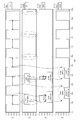
図12は、例えば複数のフリップフロップ72a,72b,72c,72d,72eを備え、フリップフロップ72a,72b間に論理回路77が設けられ、フリップフロップ72b,72c間に論理回路78が設けられ、フリップフロップ72c,72d間に論理回路79が設けられ、フリップフロップ72d,72e間に論理回路80が設けられた信号処理装置71を示す。この場合、信号処理装置71は、フリップフロップ72a、論理回路77、フリップフロップ72b、論理回路78、フリップフロップ72c、論理回路79、フリップフロップ72d、論理回路80、およびフリップフロップ72eの順にデータが供給され、各論理回路77,78,79,80により順番にデータを用いた演算処理等が実行され得るようになされている。
かかる構成に加えて、この信号処理装置71は、論理回路77に対しタイミングエラー推測部7aおよびクロック信号制御部17が設けられ、論理回路78に対しタイミングエラー推測部7bおよびクロック信号制御部17が設けられ、論理回路79に対しタイミングエラー推測部7cおよびクロック信号制御部17が設けられ、論理回路80に対しタイミングエラー推測部7dおよびクロック信号制御部17が設けられた構成を有する。この場合、タイミングエラー推測部7a,7b,7c,7dとクロック信号制御部17は、図1に示したタイミングエラー推測部7とクロック信号制御部17と同じ構成を有していることから、ここではその説明は省略する。
なお、図12では、4つの論理回路77,78,79,80を備え、各論理回路77,78,79,80のチェックポイントC1,C2,C3,C4に対し、対応するタイミングエラー推測部7a,7b,7c,7dが設けられている場合について述べるが、あくまでこれは一例であり、2つや3つ等その他複数の論理回路を設け、当該論理回路のチェックポイント(処理途中)に対してそれぞれタイミングエラー推測部を設けるようにしてもよい。
因みに、この信号処理装置71では、各論理回路77,78,79,80に対するタイミングエラー推測部7a,7b,7c,7dおよびクロック信号制御部17の接続構成が同じであることから、ここでは主に論理回路77に着目して以下説明する。この場合、論理回路77は、図1と同様に、第1論理ブロック77aおよび第2論理ブロック77b間の処理途中となるチェックポイントC1にタイミングエラー推測部7aが接続されている。これにより、タイミングエラー推測部7aは、第1論理ブロック77aで処理されたデータを、チェックポイントC1を介して論理回路77から抽出し、その時点で、第1論理ブロック77aの演算処理がクロック信号CKの前半部分末端の立ち下がりエッジ前まで(立ち上がり期間中)に終了しているか否かを判断し得る。
各タイミングエラー推測部7a,7b,7c,7dは、それぞれ対応する論理回路77,78,79,80において処理途中の段階でデータがクロック信号CKに対して既にタイミングがずれているか否かを判断し、当該タイミングがずれていれば、対応する論理回路77,78,79,80で想定した時間内に演算処理を終了し得ないと推測し得るようになされている。このように、各タイミングエラー推測部7a,7b,7c,7dは、それぞれ対応した論理回路77,78,79,80において演算処理の途中段階で、論理回路77,78,79,80が正しいタイミングで動作しているか否かを推測し得る。
これに加えて、この信号処理装置71には、タイミングエラー推測部7aおよびクロック信号制御部17間、タイミングエラー推測部7bおよびクロック信号制御部17間、タイミングエラー推測部7cおよびクロック信号制御部17間に、信号統合判定部としての論理和回路75a,75b,75cがそれぞれ設けられており、例えばタイミングエラー推測部7aの出力部が論理和回路75aを介してクロック信号制御部17の入力部に接続されている。論理和回路75aには、一方の入力部にタイミングエラー推測部7aの出力部が接続されているとともに、他方の入力部に、後段の信号統合判定部たる論理和回路75bの出力部が接続されており、タイミングエラー推測部7aからのデータと、後段の論理和回路75bからのデータとの論理和をとり得る。
これにより、例えば論理和回路75aは、タイミングエラー推測部7aから推測タイミングエラー信号STE_1を受け取るか、後段の論理和回路75bから出力された推測タイミングエラー信号STE(図示せず)を受け取るか、或いはその両方の場合、推測タイミングエラー信号STEを生成して、これをクロック信号制御部17のラッチ回路19に送出し得る。
ラッチ回路19は、対応する論理和回路75aから推測タイミングエラー信号STEを受け取ると、上述した第1の実施の形態と同様に、クロック信号CKをゲーティングしたゲーティングクロック信号GCKを生成して、これを出力部に接続されたフリップフロップ72aに送出する。これによりフリップフロップ72aは、ゲーティングクロック信号GCKの新たな立ち上がり期間に同期して正しいタイミングで処理動作を実行し得る。なお、図12では、図1にて論理積回路20の入力部に設けた否定を示す「○」を、ラッチ回路19の出力部に設けているが、図1と同様に論理和回路20の入力部に設けてもよい。
同様に、論理和回路75aの後段にある論理和回路75bでも、タイミングエラー推測部7bから推測タイミングエラー信号STE_2を受け取るか、後段の論理和回路75cから出力された推測タイミングエラー信号STE(図示せず)を受け取るか、或いはその両方の場合、推測タイミングエラー信号STEを生成して、これをクロック信号制御部17のラッチ回路19(図12ではクロック信号制御部17の構成が全て同じであるため付番省略。以下同様)に送出し得る。
このラッチ回路19でも、対応する論理和回路75bから推測タイミングエラー信号STEを受け取ると、上述した第1の実施の形態と同様に、クロック信号CKをゲーティングしたゲーティングクロック信号GCKを生成して、これを出力部に接続されたフリップフロップ72bに送出する。これにより、フリップフロップ72bは、ゲーティングクロック信号GCKの新たな立ち上がり期間に同期して正しいタイミングで処理動作を実行し得る。この際、この論理和回路75bの前段にある論理和回路75aでも、上述したように後段の論理和回路75bから受け取った推測タイミングエラー信号STEを基に、ゲーティングクロック信号GCKをラッチ回路19に生成させ得る。これにより、後段のフリップフロップ72bだけでなく前段のフリップフロップ72aも、ゲーティングクロック信号GCKの新たな立ち上がり期間に同期して正しいタイミングで処理動作を実行し得る。
同様に、論理和回路75bの後段にある論理和回路75cでも、タイミングエラー推測部7cから推測タイミングエラー信号STE_3を受け取るか、後段のタイミングエラー推測部7dから出力された推測タイミングエラー信号STE_4を受け取るか、或いはその両方の場合、推測タイミングエラー信号STEを生成して、これをクロック信号制御部17のラッチ回路19に送出し得る。なお、この実施の形態の場合、フリップフロップ72eの後段にタイミングエラー推測部を設けていないことから、最後尾のタイミングエラー推測部7dおよびクロック信号制御部17間には、信号統合判定部たる論理和回路が設けられておらず、最後尾のタイミングエラー推測部7dにて生成された推測タイミングエラー信号STE_4は、クロック信号制御部17と、前段の論理和回路75cとにそのまま送出され得る。
この際、最後尾のタイミングエラー推測部7dよりも前段にある全ての論理和回路75a,75b,75cは、最後尾のタイミングエラー推測部7dにて生成された推測タイミングエラー信号STE_4を基に推測タイミングエラー信号STEをそれぞれ生成し、当該推測タイミングエラー信号STEに基づいて各ラッチ回路19によりゲーティングクロック信号GCKを生成させ得る。これにより、推測タイミングエラー信号STE_4を生成したタイミングエラー推測部7dを有する論理回路80の前段にある全てのフリップフロップ72a,72b,72c,72dは、各クロック信号制御部17から出力されたゲーティングクロック信号GCKの新たな立ち上がり期間に同期し、正しいタイミングで処理動作を実行し得る。
以上の構成において、信号処理装置71では、複数のタイミングエラー推測部7a,7b,7c,7dのいずれかで、論理回路77,78,79,80での処理途中の段階でデータがクロック信号CKに対してタイミングがずれていると推測すると、例えばタイミングがずれている論理回路(エラー推測論理回路)79と、この論理回路79の前段にある論理回路77,78とに対しクロック信号の供給を制御させる信号統合判定部として論理和回路75a,75b,75cを設けるようにした。これにより、信号処理装置71では、タイミングがずれていると推測した論理回路79を含め、この論理回路79の前段にある全ての論理回路77,78に対してだけ、タイミングエラー推測部7cにて得られたタイミングエラー発生の推測結果を反映させることができ、動作不良を生じる虞のある最低限の論理回路77,78,79だけクロック信号CKをゲーティングすることができる。
なお、上述した図12では、図1に示したタイミングエラー推測部7と同じ構成のタイミングエラー推測部7a,7b,7c,7dを各論理回路77,78,79,80のチェックポイントC1,C2,C3,C4に接続させた信号処理装置71について述べたが、本発明はこれに限らず、図5に示したタイミングエラー推測部37と同じ構成のタイミングエラー推測部を各論理回路77,78,79,80のチェックポイントC1,C2,C3,C4に接続させた信号処理装置としてもよい。
また、図12との対応部分に同一符号を付して示す図13は、例えば、図1に示したタイミングエラー推測部7、または図5に示したタイミングエラー推測部37のいずれかと同じ構成を有した複数のタイミングエラー推測部37a,37b,37c,37dを備えた信号処理装置81を示している。この信号処理装置81は、より具体的に示したもので、これら複数のタイミングエラー推測部37a,37b,37c,37dに共通の配線を設けて、当該配線によりクロック信号CKを各タイミングエラー推測部37a,37b,37c,37dに供給し得る構成としてもよい。
なお、上述した全ての実施の形態においては、タイミングエラー推測部7,37,37a,37b,37c,37dや、クロック信号制御部17、信号統合判定部60,65、論理和回路(信号統合判定部)75a,75b,75c,75d、第1遅延部46、第2遅延部47、第3遅延部48について、上述したような構成とした場合について述べたが、本発明はこれに限らず、その他種々のトランジスタや、論理回路等を組み合わせた種々のタイミングエラー推測部や、クロック信号制御部、信号統合判定部、第1遅延部、第2遅延部、第3遅延部を適用してもよい。
なお、上述した実施の形態においては、送り側および受け側のフリップフロップ間に1つのチェックポイントを設け、当該チェックポイントにタイミングエラー推測部を設けた信号処理装置について述べたが、本発明はこれに限らず、例えば送り側および受け側のフリップフロップ間に複数のチェックポイントを設け、これらチェックポイントにそれぞれタイミングエラー推測部を設けた信号処理装置としてもよい。このような信号処理装置では、図11Aに示した信号統合判定部60や、図11Bに示した信号統合判定部65を利用して、送り側および受け側のフリップフロップ間の各タイミングエラー推測部から得られた推測タイミングエラー信号を基に、1つの推測タイミングエラー信号STEを生成し得、上述した実施の形態と同様の効果を得ることができる。
1,31,56,71 信号処理装置
4,34,54 乗算器(論理回路)
7,37,37a,37b,37c,37d タイミングエラー推測部
8 遷移検出部
9,39 エラー判断部
17 クロック信号制御部
40,45 検出用クロック信号生成回路
46 第1遅延部(遅延部)
47 第2遅延部(遅延部)
48 第3遅延部(遅延部)
58,59 論理回路
60,65 信号統合判定部
75a,75b,75c 論理和回路(信号統合判定部)
4,34,54 乗算器(論理回路)
7,37,37a,37b,37c,37d タイミングエラー推測部
8 遷移検出部
9,39 エラー判断部
17 クロック信号制御部
40,45 検出用クロック信号生成回路
46 第1遅延部(遅延部)
47 第2遅延部(遅延部)
48 第3遅延部(遅延部)
58,59 論理回路
60,65 信号統合判定部
75a,75b,75c 論理和回路(信号統合判定部)
Claims (9)
- 所定のクロック信号に同期させ所定のタイミングでデータを処理して出力する論理回路から処理途中のデータを取得し、処理途中の段階で該データが前記クロック信号に対してタイミングがずれているか否かを判断するタイミングエラー推測部を備える
ことを特徴とする信号処理装置。 - 前記タイミングエラー推測部は、
前記データの立ち上がりから立ち下がり、または立ち下がりから立ち上がりの遷移を検出する遷移検出部と、
前記データの遷移を前記クロック信号の立ち下がり期間中に検出したとき、該データが前記クロック信号に対しタイミングがずれていると推測するエラー判断部と
を備えることを特徴とする請求項1記載の信号処理装置。 - 前記データが前記クロック信号に対しタイミングがずれていると推測したとき、前記論理回路に対する前記クロック信号の供給を制御するクロック信号制御部を備える
ことを特徴とする請求項1または2記載の信号処理装置。 - 前記タイミングエラー推測部は、
前記論理回路から処理途中のデータを取得する位置に対応して、前記クロック信号の立ち上がりおよび立ち下がりのデューティ比を可変した検出用クロック信号を生成する検出用クロック信号生成部を備え、前記データが前記検出用クロック信号に対してタイミングがずれているか否かを判断する
ことを特徴とする請求項1~3のうちいずれか1項記載の信号処理装置。 - 前記検出用クロック信号生成部は、複数の遅延部を備えており、
各前記遅延部は、前記クロック信号を遅延させ、該クロック信号の立ち上がりおよび立ち下がりのデューティ比が異なる前記検出用クロック信号を生成する
ことを特徴とする請求項4記載の信号処理装置。 - 複数の前記論理回路により前記データを順番に処理する構成を有しており、
各前記論理回路には前記タイミングエラー推測部が設けられ、各前記タイミングエラー推測部毎に、対応する前記論理回路から処理途中のデータを取得し、処理途中の段階で該データが前記クロック信号に対してタイミングがずれているか否かを判断する
ことを特徴とする請求項1~5のうちいずれか1項記載の信号処理装置。 - 複数の前記タイミングエラー推測部のいずれかで、前記論理回路での処理途中の段階で前記データが前記クロック信号に対してタイミングがずれていると推測したとき、複数の前記論理回路全てに対し前記クロック信号の供給を制御させる信号統合判定部を備える
ことを特徴とする請求項6記載の信号処理装置。 - 複数の前記タイミングエラー推測部のいずれかで、前記論理回路での処理途中の段階で前記データが前記クロック信号に対してタイミングがずれていると推測したとき、前記タイミングがずれている前記論理回路と、該論理回路の前段の他の論理回路全てとに対し前記クロック信号の供給を制御する信号統合判定部を備える
ことを特徴する請求項6記載の信号処理装置。 - 所定のクロック信号に同期させ所定のタイミングでデータを処理して出力する論理回路から処理途中のデータを取得し、タイミングエラー推測部によって、処理途中の段階で該データが前記クロック信号に対してタイミングがずれているか否かを判断する
ことを特徴とする信号処理方法。
Priority Applications (1)
| Application Number | Priority Date | Filing Date | Title |
|---|---|---|---|
| JP2015502876A JPWO2014132843A1 (ja) | 2013-02-27 | 2014-02-18 | 信号処理装置および信号処理方法 |
Applications Claiming Priority (2)
| Application Number | Priority Date | Filing Date | Title |
|---|---|---|---|
| JP2013037620 | 2013-02-27 | ||
| JP2013-037620 | 2013-02-27 |
Publications (1)
| Publication Number | Publication Date |
|---|---|
| WO2014132843A1 true WO2014132843A1 (ja) | 2014-09-04 |
Family
ID=51428114
Family Applications (1)
| Application Number | Title | Priority Date | Filing Date |
|---|---|---|---|
| PCT/JP2014/053813 Ceased WO2014132843A1 (ja) | 2013-02-27 | 2014-02-18 | 信号処理装置および信号処理方法 |
Country Status (2)
| Country | Link |
|---|---|
| JP (1) | JPWO2014132843A1 (ja) |
| WO (1) | WO2014132843A1 (ja) |
Cited By (1)
| Publication number | Priority date | Publication date | Assignee | Title |
|---|---|---|---|---|
| CN115694438A (zh) * | 2023-01-04 | 2023-02-03 | 华中科技大学 | 一种轻量级宽电压域时序错误检测单元 |
Citations (2)
| Publication number | Priority date | Publication date | Assignee | Title |
|---|---|---|---|---|
| JPS61501124A (ja) * | 1984-05-23 | 1986-05-29 | モトロ−ラ・インコ−ポレ−テッド | パルスの欠如または余剰パルスを検出するパルス検出器 |
| JP2012516629A (ja) * | 2009-01-27 | 2012-07-19 | アギア システムズ インコーポレーテッド | 性能監視用クリティカルパス回路 |
-
2014
- 2014-02-18 JP JP2015502876A patent/JPWO2014132843A1/ja active Pending
- 2014-02-18 WO PCT/JP2014/053813 patent/WO2014132843A1/ja not_active Ceased
Patent Citations (2)
| Publication number | Priority date | Publication date | Assignee | Title |
|---|---|---|---|---|
| JPS61501124A (ja) * | 1984-05-23 | 1986-05-29 | モトロ−ラ・インコ−ポレ−テッド | パルスの欠如または余剰パルスを検出するパルス検出器 |
| JP2012516629A (ja) * | 2009-01-27 | 2012-07-19 | アギア システムズ インコーポレーテッド | 性能監視用クリティカルパス回路 |
Cited By (2)
| Publication number | Priority date | Publication date | Assignee | Title |
|---|---|---|---|---|
| CN115694438A (zh) * | 2023-01-04 | 2023-02-03 | 华中科技大学 | 一种轻量级宽电压域时序错误检测单元 |
| CN115694438B (zh) * | 2023-01-04 | 2023-03-17 | 华中科技大学 | 一种轻量级宽电压域时序错误检测单元 |
Also Published As
| Publication number | Publication date |
|---|---|
| JPWO2014132843A1 (ja) | 2017-02-02 |
Similar Documents
| Publication | Publication Date | Title |
|---|---|---|
| JP6561172B2 (ja) | レシプロカル量子論理(rql)回路合成 | |
| TWI548886B (zh) | 老化偵測電路及其方法 | |
| CN107836094B (zh) | 时钟恢复电路 | |
| US11842199B2 (en) | Controlling the operating speed of stages of an asynchronous pipeline | |
| TW201937856A (zh) | 用於保護數位電路免受時間誤差之方法及安排 | |
| KR102779209B1 (ko) | 테스트 회로, 테스트 방법 및 테스트 회로를 포함하는 계산 시스템 | |
| US10310994B2 (en) | Asynchronous finite state machines | |
| JP2008064752A (ja) | Pd−soiテクノロジにおけるスイッチング遅延ヒストリ効果のインライン計測の方法及び装置 | |
| TWI586107B (zh) | Timing Error Detection and Correction Device and Its Normal Timing Design Method | |
| Lorenz et al. | Monitoring of aging in integrated circuits by identifying possible critical paths | |
| US20110295536A1 (en) | Clock jitter analyzing method and apparatus | |
| WO2014132843A1 (ja) | 信号処理装置および信号処理方法 | |
| Shin et al. | A pipeline architecture with 1-cycle timing error correction for low voltage operations | |
| Hiienkari et al. | A 3.15 pJ/cyc 32-bit RISC CPU with timing-error prevention and adaptive clocking in 28nm CMOS | |
| Garg | Common path pessimism removal: An industry perspective: Special session: Common path pessimism removal | |
| JP2014140107A (ja) | パルス測定回路及びデータ処理装置 | |
| JP2008042367A (ja) | 半導体装置 | |
| EP1570599B1 (en) | System and method of digital system performance enhancement | |
| WO2012164541A1 (en) | Method and circuit for solving metastability conditions and recovering signal errors in digital integrated circuits | |
| JP2013061811A (ja) | 消費電力解析方法および消費電力解析装置 | |
| Stepchenkov et al. | Speed-independent fused multiply add and subtract unit | |
| Ahmadi et al. | A timing error mitigation technique for high performance designs | |
| US9379720B1 (en) | Clock recovery circuit | |
| US9960771B2 (en) | Hum generation using representative circuitry | |
| KR101162259B1 (ko) | 반도체 집적회로 및 그의 구동 방법 |
Legal Events
| Date | Code | Title | Description |
|---|---|---|---|
| 121 | Ep: the epo has been informed by wipo that ep was designated in this application |
Ref document number: 14757344 Country of ref document: EP Kind code of ref document: A1 |
|
| ENP | Entry into the national phase |
Ref document number: 2015502876 Country of ref document: JP Kind code of ref document: A |
|
| NENP | Non-entry into the national phase |
Ref country code: DE |
|
| 122 | Ep: pct application non-entry in european phase |
Ref document number: 14757344 Country of ref document: EP Kind code of ref document: A1 |