WO2014126118A1 - 薄型表示装置 - Google Patents
薄型表示装置 Download PDFInfo
- Publication number
- WO2014126118A1 WO2014126118A1 PCT/JP2014/053236 JP2014053236W WO2014126118A1 WO 2014126118 A1 WO2014126118 A1 WO 2014126118A1 JP 2014053236 W JP2014053236 W JP 2014053236W WO 2014126118 A1 WO2014126118 A1 WO 2014126118A1
- Authority
- WO
- WIPO (PCT)
- Prior art keywords
- gasket
- plate member
- hole
- metal plate
- disposed
- Prior art date
- Legal status (The legal status is an assumption and is not a legal conclusion. Google has not performed a legal analysis and makes no representation as to the accuracy of the status listed.)
- Ceased
Links
Images





Classifications
-
- G—PHYSICS
- G02—OPTICS
- G02F—OPTICAL DEVICES OR ARRANGEMENTS FOR THE CONTROL OF LIGHT BY MODIFICATION OF THE OPTICAL PROPERTIES OF THE MEDIA OF THE ELEMENTS INVOLVED THEREIN; NON-LINEAR OPTICS; FREQUENCY-CHANGING OF LIGHT; OPTICAL LOGIC ELEMENTS; OPTICAL ANALOGUE/DIGITAL CONVERTERS
- G02F1/00—Devices or arrangements for the control of the intensity, colour, phase, polarisation or direction of light arriving from an independent light source, e.g. switching, gating or modulating; Non-linear optics
- G02F1/01—Devices or arrangements for the control of the intensity, colour, phase, polarisation or direction of light arriving from an independent light source, e.g. switching, gating or modulating; Non-linear optics for the control of the intensity, phase, polarisation or colour
- G02F1/13—Devices or arrangements for the control of the intensity, colour, phase, polarisation or direction of light arriving from an independent light source, e.g. switching, gating or modulating; Non-linear optics for the control of the intensity, phase, polarisation or colour based on liquid crystals, e.g. single liquid crystal display cells
- G02F1/133—Constructional arrangements; Operation of liquid crystal cells; Circuit arrangements
- G02F1/1333—Constructional arrangements; Manufacturing methods
- G02F1/1335—Structural association of cells with optical devices, e.g. polarisers or reflectors
- G02F1/1336—Illuminating devices
- G02F1/133602—Direct backlight
- G02F1/133608—Direct backlight including particular frames or supporting means
-
- G—PHYSICS
- G02—OPTICS
- G02F—OPTICAL DEVICES OR ARRANGEMENTS FOR THE CONTROL OF LIGHT BY MODIFICATION OF THE OPTICAL PROPERTIES OF THE MEDIA OF THE ELEMENTS INVOLVED THEREIN; NON-LINEAR OPTICS; FREQUENCY-CHANGING OF LIGHT; OPTICAL LOGIC ELEMENTS; OPTICAL ANALOGUE/DIGITAL CONVERTERS
- G02F1/00—Devices or arrangements for the control of the intensity, colour, phase, polarisation or direction of light arriving from an independent light source, e.g. switching, gating or modulating; Non-linear optics
- G02F1/01—Devices or arrangements for the control of the intensity, colour, phase, polarisation or direction of light arriving from an independent light source, e.g. switching, gating or modulating; Non-linear optics for the control of the intensity, phase, polarisation or colour
- G02F1/13—Devices or arrangements for the control of the intensity, colour, phase, polarisation or direction of light arriving from an independent light source, e.g. switching, gating or modulating; Non-linear optics for the control of the intensity, phase, polarisation or colour based on liquid crystals, e.g. single liquid crystal display cells
- G02F1/133—Constructional arrangements; Operation of liquid crystal cells; Circuit arrangements
- G02F1/1333—Constructional arrangements; Manufacturing methods
- G02F1/1335—Structural association of cells with optical devices, e.g. polarisers or reflectors
- G02F1/1336—Illuminating devices
- G02F1/133602—Direct backlight
- G02F1/133603—Direct backlight with LEDs
Definitions
- the present invention relates to a thin display device and, for example, to a thin display device having a function of securing a ground using a gasket between a circuit board (printed circuit board) and a metal plate.
- a resin backlight cover covers the metal plate member on which the LED is placed as the backlight, and the main PWB (printed board) The structure which attaches is known.
- FIG. 1 the attachment structure of the gasket 190 with respect to main PWB150 in a liquid crystal display device is demonstrated here.
- a gasket (conductive member) 190 is fixed to the PWB back surface 151 where the ground (GND) of the main PWB 150 is formed with a double-sided tape.
- FIG. 1B in the set in which the resin back cabinet 120 is disposed on the back side (the upper side in the drawing) of the metal plate member 130 with the gasket 190 fixed to the main PWB 150.
- the gasket 190 is affixed to a predetermined region of the metal plate member 130 with a double-sided tape through the gasket penetration hole 140 formed in the back cabinet 120.
- FIG. 1C the structure shown in FIG. 1C is obtained, and the main PWB 150 and the metal plate member 130 are appropriately brought into contact with each other via the gasket 190 to ensure conduction.
- Patent Document 1 there is a technique for further reducing the thickness of a communication portable terminal having a built-in antenna while preventing the result of antenna characteristics.
- a first resin cabinet in which the first sheet metal is insert-molded and a second resin cabinet in which the second sheet metal is insert-molded are provided.
- a circuit board on which an antenna is printed is sandwiched between the first resin cabinet and the second resin cabinet, and the first sheet metal, the second sheet metal, and the antenna are separated by a plurality of conductive gaskets. Electrically connected.
- the gasket 190 is fixed to the main PWB 150 and the metal plate member 130 only by double-sided tape. Moreover, since the back cabinet 120 is fixed through the gasket through-holes 140, the TV adopting such a structure has problems such as deterioration of the adhesive property of the double-sided tape and variation in the way of attachment during assembly. It was. For example, as shown in FIG. 1D, it is assumed that the gasket 190 is detached from the gasket penetration hole 140 due to deformation or the like. When these problems become apparent, the gasket 190 that electrically connects the main PWB 150 and the metal plate member 130 may become unstable in contact and may deteriorate unnecessary radiation, or may come into contact with other parts and have an adverse effect. Also, in order to prevent such products from being shipped to the market, the labor of the inspection process has increased and countermeasures have been required.
- Patent Document 1 a conductive material that is far away is electrically connected and effectively used by using a gasket.
- positioning is performed by fixing with a double-sided tape or by making a hole in an intermediate resin cabinet.
- another technique has been demanded because deformation due to compression of the gasket cannot be suppressed and there is a possibility of contact with a non-contactable area.
- an adhesive such as double-sided tape is peeled off, the gasket may move due to vibration or the like, and another countermeasure is required because countermeasures are required.
- the present invention has been made in view of the above situation, and an object thereof is to provide a technique for solving the above problems.
- a thin display device of the present invention a metal plate member disposed on the back side of the display panel, a non-conductive plate member provided with a through-hole, disposed on the back side of the metal plate member, A circuit board disposed opposite to the back surface side with respect to the non-conductive plate member, and a gasket disposed in the through-hole to maintain electrical connection between the metal plate member and the circuit board
- the non-conductive plate member includes a gasket fixing portion formed in a convex shape around the through hole.
- the gasket may be thicker than the gasket fixing portion.
- the gasket fixing portion may be a wall surface formed around the through hole.
- the gasket fixing portion may have a claw shape that is engaged with a side surface of the gasket.
- the structure of the through hole of the backlight cover which is a resin member, that penetrates when contacting the circuit board and the metal plate member is improved so that the gasket can be mechanically fixed.
- Technology can be provided.
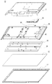
- FIG. 2 is an exploded perspective view of the liquid crystal television 10 according to the present embodiment, which is schematically displayed by arranging the front side on the lower side in the drawing and the back side on the upper side in the drawing.
- a backlight unit 30 is disposed opposite to the back side (upper side in the figure) of the display panel 12.
- a front cabinet 11 is disposed on the front side (lower side in the figure) of the display panel 12.
- the backlight unit 30 is a so-called direct type backlight, and a plurality of LEDs are disposed as light sources on the front side of the metal plate member. Further, a resin-made backlight cabinet 20 is disposed on the back side of the backlight unit 30 so as to face each other. Further, the main PWB 50 is arranged to face a predetermined area on the back side. Further, the rear cabinet 13 is disposed to face the back side of the backlight cabinet 20 to which the main PWB 50 is attached.
- the backlight cabinet 20 is provided with a gasket arrangement portion 40 that communicates with the front and rear of the backlight cabinet 20.
- a gasket 90 having a predetermined size is arranged in the gasket arrangement portion 40, and a predetermined rectangular area 35 of the metal plate member of the backlight unit 30 and a predetermined ground circuit area (ground pattern) of the main PWB 50 are electrically connected. Connected.
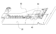
- FIG. 3 The perspective view of FIG. 3 focuses on the backlight cabinet 20 and the main PWB 50.
- the main PWB 50 is disposed and fixed on the back surface of the backlight cabinet 20. At this time, the main PWB 50 is grounded to the backlight unit 30 by the gasket 90.
- Various processing LSIs, input / output terminals, and the like are arranged on the upper surface on the back side (upper side in the figure) of the main PWB 50.
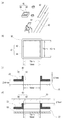
- FIG. 4 is a view focusing on the gasket arrangement portion of the ground structure.
- FIG. 5 is a diagram showing a procedure for forming a grounding structure using a gasket.
- FIG. 5C corresponds to the AA cross section of FIG.
- the backlight cabinet 20 is formed with a gasket arrangement portion 40 for arranging the gasket 90.
- the gasket 90 is a cube having a size of 15 mm ⁇ 15 mm ⁇ 15 mm, and has a cushioning property that can be crushed by a certain amount.
- the gasket placement portion 40 is formed of a rectangular gasket penetration opening 42 and a wall portion 44 surrounding the four sides of the gasket penetration opening 42.
- the wall 44 may be formed mainly around the area corresponding to the lower side when the liquid crystal television 10 is used upright. It does not have to be formed in a region corresponding to. However, in consideration of the case where the gasket 90 is displaced and deformed with the movement of the main PWB 50 or the like, it is preferably formed also in the upper side region. In addition, there is no way to completely form the wall surface, and a plurality of pin-like structures may be used.
- the gasket penetration opening 42 has a size of 16 mm ⁇ 16 mm. Therefore, in the state where the gasket 90 is disposed, a gap of 0.5 mm in the vertical and horizontal directions is formed between the gasket 90 and the outer peripheral portion of the gasket penetration opening 42.
- the wall portion 44 is formed with a predetermined width so as to surround the gasket penetration opening 42 in a convex shape with a height of 3.5 mm on the back side.
- the thickness of the plate-shaped part of the backlight cabinet 20 is 3.0 mm.
- the distance between the backlight unit 30 (metal plate member 32) and the backlight cabinet 20 is 2.55 mm.
- the distance between the front end of the wall 44 and the main PWB 50 is 2.5 mm. That is, the distance between the metal plate member 32 on the back side of the backlight unit 30 and the main PWB 50 is 11.55 mm, and the gasket 90 is fixed in a state of being crushed by 3.45 mm.
- a rectangular area 35 of 18 mm in width and 15 mm in length is secured as a grounding area in the area where the gasket 90 is fixed on the front side of the main PWB 50 (the lower side in the figure and facing the backlight cabinet 20). Has been.
- positioning procedure of the grounding structure by a gasket is demonstrated.
- the gasket 90 is inserted into the gasket placement portion 40, and the backlight unit 30 is predetermined. Are disposed in the grounding area 35. At this time, the gasket 90 remains in its original form.
- the main PWB 50 is disposed from above the gasket 90, that is, from the back side.
- the distance between the main PWB 50 and the backlight cabinet 20 is set to 2.5 mm as described with reference to FIG. Therefore, as shown in FIG. 5C, the main PWB 50 is fixed to the backlight cabinet 20, whereby the gasket 90 is crushed and fixed by a predetermined amount.
- the length of the gasket 90 protruding from the upper end of the wall portion 44 of the gasket arrangement portion 40 is 5.5 mm from 8.95 mm before being crushed.
- the mechanical strength of the gasket fixing is ensured. That is, the width and area facing the side surface of the gasket 90 increase. For this reason, the shape deformation of the gasket 90 can be controlled during the mounting operation of the gasket 90. Therefore, displacement due to vibration or the like is suppressed, and positioning at the time of attaching the gasket 90 is facilitated. Moreover, the stable contact and conduction
- FIG. 6 is a view showing a gasket arrangement portion 40 according to the second embodiment.
- a claw-like locking structure 46 may be formed on the inner surface of the wall portion 44.
- the gasket 90 is more firmly fixed.
- the locking structure 46 may be formed over the entire inner surface, or may be formed only in a partial region.
- the size of the locking structure 46 is set in consideration of the workability when the gasket 90 is disposed, the amount of deformation when the gasket 90 is crushed, and the balance of the fixing force. It is about 0.5 mm corresponding to a gap with 40. Further, as shown in FIG.
- holes 48 may be provided at two opposing portions of the wall portion 44, and the fixing bars 49 may be attached to these holes 48 so as to pierce and penetrate the gasket 90.
- the number of fixing bars 49 penetrating the gasket 90 is not limited to one, and a plurality of fixing bars 49 may be used, or a structure that does not penetrate may be used.
- the height of the wall portion 44 of the gasket placement portion 40 may be lowered only on the cushion portion surface of the gasket 90.
- the gasket 90 is deformed by creating a cushion escape space for the crushed gasket 90, contact with other than the ground pattern can be prevented.
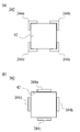
- FIG. 7 is a view showing gasket arrangement portions 240 and 340 according to the third embodiment, and corresponds to FIG.
- the gasket placement portion 240 shown in FIG. 7A has a configuration corresponding to the above-described wall portion 44 surrounding the periphery of the gasket penetration opening 42, and the first to fourth portions formed at the four corners of the gasket penetration opening 42.
- Protrusions 244a to 244d are provided.
- the first to fourth protrusions 244a to 244d have an L-shaped rib protrusion structure in a top view.
- the gasket placement portion 340 shown in FIG. 7B has a plate-like (rib-like) shape in the vicinity of the four sides of the gasket penetration opening 42 as a configuration corresponding to the wall portion 44 surrounding the periphery of the gasket penetration opening 42.
- First to fourth wall portions 344a to 344d are provided. Contrary to the configuration of FIG. 7A, the four corners of the wall portion 44 are removed.
- the crushed portion is not formed with the first to fourth protrusions 244a to 244d and the first to fourth wall portions 344a to 344d. Since it fits in the four spaces, the position maintaining function of the gasket 90 works well against vibrations in all directions.
- FIG. 8 is a cross-sectional side view showing a gasket arrangement portion 440 according to the fourth embodiment, and corresponds to FIG.
- the gasket placement portion 440 is formed with a wall portion 444 that protrudes up and down so as to surround the gasket penetration opening 442, that is, a wall portion 444 that protrudes on both sides of the main PWB 50 and the backlight unit 30.
- the gasket penetration opening 442 is formed in the inner wall surface of the wall part 444 so that the backlight unit 30 side may spread. That is, the gasket penetration opening 442 is a truncated quadrangular pyramid.
- the upper size of the gasket penetration opening 442 is substantially the same as the outer shape of the gasket 90.
- the gasket 90 is inserted into the gasket penetration opening 442 from above, and the state shown in FIG. 8B is obtained.
- a predetermined space X is formed between the wall portion 444 and the gasket 90.
- FIG. 8C when the main PWB 50 is attached and the gasket 90 is crushed and deformed, the deformed portion swells into the space X between the wall portion 444 and the gasket 90. As a result, the deformed portion does not protrude from the main PWB 50 side. Therefore, the gasket 90 does not adversely affect the components and wiring mounted on the main PWB 50.
- FIG. 9 is a cross-sectional side view showing a gasket arrangement portion 540 according to the fifth embodiment.
- an upper side wall portion 544a formed so as to surround the upper side of the gasket penetration opening 542, and a first lower side wall portion 544b and a second lower side wall portion 544c formed on the lower side are provided.
- the upper wall portion 544a has a structure similar to that of the wall portion 40 shown in FIG. 6A, and a claw-like locking structure 546 is formed on the upper inner surface of the upper wall portion 544a.
- the gasket 90 that is locked to the locking structure 546 is formed with a predetermined cut or concave shape for determining the locking position.
- the first lower wall portion 544b corresponds to two wall portions on the back side and the near side (not shown) in the drawing. These first lower side wall portions 544b are formed in a rib shape extending vertically downward by a predetermined length.
- the second lower wall portion 544c corresponds to the two left and right wall portions in the drawing. These second lower side wall portions 544c have a structure that spreads outward.
Landscapes
- Physics & Mathematics (AREA)
- Nonlinear Science (AREA)
- Mathematical Physics (AREA)
- Chemical & Material Sciences (AREA)
- Crystallography & Structural Chemistry (AREA)
- General Physics & Mathematics (AREA)
- Optics & Photonics (AREA)
- Devices For Indicating Variable Information By Combining Individual Elements (AREA)
- Liquid Crystal (AREA)
- Transforming Electric Information Into Light Information (AREA)
Abstract
Description
また、前記ガスケットは、前記ガスケット固定部より厚くてもよい。
また、前記ガスケット固定部は、前記貫通孔の周囲に形成された壁面であってもよい。
また、前記ガスケット固定部は、前記ガスケットの側面に係止するツメ形状を備えてもよい。
また、前記ガスケット固定部に形成された孔と、前記孔を貫通して前記ガスケットに刺さる棒状体とを備えてもよい。
図2は、本実施形態に係る液晶テレビ10の分解斜視図であり、正面側が図中下側に、背面側が図中上側になるように配置して模式的に表示している。
まず、図5(a)に示すように、バックライトキャビネット20がバックライトユニット30の背面側に適正に配置された状態で、ガスケット配置部40にガスケット90が挿入され、バックライトユニット30の所定の接地用の領域35に配置される。このとき、ガスケット90は原形をとどめたままである。
図6は第2の実施形態に係るガスケット配置部40を示した図である。例えば図6(a)に示すように、壁部44の内面に爪状の係止構造46が形成されてもよい。ガスケット90の固定が一層強固になる。係止構造46は、内面全周にわたって形成されてもよいし、一部領域のみに形成されてもよい。また、係止構造46の大きさは、ガスケット90を配置するときの作業性、潰れたときの変形量及び固定力のバランスを考慮して設定されており、例えば、上記ガスケット90とガスケット配置部40とのギャップに相当する0.5mm程度である。また、図6(b)に示すように、壁部44の対向する2カ所に穴48が設けられ、固定用バー49がガスケット90を突き刺し貫通するように、それら穴48に取り付けられてもよい。なお、ガスケット90を貫通する固定用バー49は一本でなく、複数であってもよく、貫通しない構成が用いられてもよい。
図7は第3の実施形態に係るガスケット配置部240、340を示す図であって、図4(b)に対応する図である。
図8は第4の実施形態に係るガスケット配置部440を示す断面側面図であって、図5に対応している。ガスケット配置部440は、ガスケット貫通用開口442を囲むように、上下に突出する、つまり、メインPWB50及びバックライトユニット30の両方の側に突出する壁部444が形成されている。そして、壁部444の内壁面はバックライトユニット30側が広がるようにガスケット貫通用開口442が形成されている。つまり、ガスケット貫通用開口442は截頭四角錐になっている。ガスケット貫通用開口442の上側の大きさは、ガスケット90の外形と略同一になっている。
図9は第5の実施形態に係るガスケット配置部540を示す断面側面図である。このガスケット配置部540では、ガスケット貫通用開口542の上側を囲むように形成された上側壁部544aと、下側に形成された第1の下側壁部544b及び第2の下側壁部544cとを有する。上側壁部544aは、図6(a)で示した壁部40と同様の構造となっており、上側壁部544aの内面上側に爪状の係止構造546が形成されている。係止構造546に係止されるガスケット90には係止位置を決めるための所定の切り目や凹状形状が形成されている。
11 フロントキャビネット
12 表示パネル
13 リヤキャビネット
20 バックライトキャビネット
30 バックライトユニット
32 金属板部材
35 領域
40、240、340、440、540 ガスケット配置部
42、442、542 ガスケット貫通用開口
44、444 壁部
46、546 係止構造
48 穴
49 固定用バー
50 メインPWB
90 ガスケット
244a~244d 第1~第4の突起部
344a~344d 第1~第4の壁部
544a 上側壁部
544b 第1の下側壁部
544c 第2の下側壁部
Claims (5)
- 表示パネルの背面側に配置された金属板部材と、
前記金属板部材に対して背面側に対向して配置され、貫通孔を備えた非導電性板部材と、
前記非導電性板部材に対して背面側に対向して配置された回路基板と、
前記貫通孔に配置され、前記金属板部材と前記回路基板との導通を保持するガスケットと、
を備え、
前記非導電性板部材は、前記貫通孔の周囲に凸状に形成されたガスケット固定部を備えることを特徴とする薄型表示装置。 - 前記ガスケットは、前記ガスケット固定部より厚いことを特徴とする請求項1に記載の薄型表示装置。
- 前記ガスケット固定部は、前記貫通孔の周囲に形成された壁面であることを特徴とする請求項1に記載の薄型表示装置。
- 前記ガスケット固定部は、前記ガスケットの側面に係止するツメ形状を備えることを特徴とする請求項1に記載の薄型表示装置。
- 前記ガスケット固定部に形成された孔と、
前記孔を貫通して前記ガスケットに刺さる棒状体とを備えることを特徴とする請求項1に記載の薄型表示装置。
Priority Applications (2)
| Application Number | Priority Date | Filing Date | Title |
|---|---|---|---|
| US14/763,716 US20150362801A1 (en) | 2013-02-14 | 2014-02-13 | Flat-panel display |
| CN201480008662.1A CN105074801A (zh) | 2013-02-14 | 2014-02-13 | 薄型显示装置 |
Applications Claiming Priority (4)
| Application Number | Priority Date | Filing Date | Title |
|---|---|---|---|
| JP2013-026554 | 2013-02-14 | ||
| JP2013026554 | 2013-02-14 | ||
| JP2014020087A JP5563728B1 (ja) | 2013-02-14 | 2014-02-05 | 薄型表示装置 |
| JP2014-020087 | 2014-02-05 |
Publications (1)
| Publication Number | Publication Date |
|---|---|
| WO2014126118A1 true WO2014126118A1 (ja) | 2014-08-21 |
Family
ID=51354117
Family Applications (1)
| Application Number | Title | Priority Date | Filing Date |
|---|---|---|---|
| PCT/JP2014/053236 Ceased WO2014126118A1 (ja) | 2013-02-14 | 2014-02-13 | 薄型表示装置 |
Country Status (4)
| Country | Link |
|---|---|
| US (1) | US20150362801A1 (ja) |
| JP (1) | JP5563728B1 (ja) |
| CN (1) | CN105074801A (ja) |
| WO (1) | WO2014126118A1 (ja) |
Families Citing this family (2)
| Publication number | Priority date | Publication date | Assignee | Title |
|---|---|---|---|---|
| JP5736492B2 (ja) * | 2013-02-14 | 2015-06-17 | シャープ株式会社 | 薄型表示装置 |
| CN121002465A (zh) | 2023-04-27 | 2025-11-21 | 三星电子株式会社 | 弹性导电构件和包括弹性导电构件的电子装置 |
Citations (8)
| Publication number | Priority date | Publication date | Assignee | Title |
|---|---|---|---|---|
| JP2003015150A (ja) * | 2001-06-28 | 2003-01-15 | Aiphone Co Ltd | 液晶パネル導電接続構造 |
| JP2005209868A (ja) * | 2004-01-22 | 2005-08-04 | Casio Comput Co Ltd | 電子機器 |
| JP2010109760A (ja) * | 2008-10-30 | 2010-05-13 | Sharp Corp | 通信携帯端末 |
| JP2010165440A (ja) * | 2009-01-19 | 2010-07-29 | Sharp Corp | ディスクドライブ搭載型表示装置,表示ユニット |
| JP2012047838A (ja) * | 2010-08-25 | 2012-03-08 | Funai Electric Co Ltd | 液晶モジュールのx−プリント回路基板の固定構造 |
| US20120182515A1 (en) * | 2011-01-19 | 2012-07-19 | Pyo Si-Baek | Liquid crystal display apparatus |
| WO2012117657A1 (ja) * | 2011-02-28 | 2012-09-07 | パナソニック株式会社 | 表示装置 |
| WO2012165324A1 (ja) * | 2011-06-02 | 2012-12-06 | シャープ株式会社 | 照明装置、表示装置、及びテレビ受信装置 |
Family Cites Families (11)
| Publication number | Priority date | Publication date | Assignee | Title |
|---|---|---|---|---|
| JP2000291802A (ja) * | 1999-04-12 | 2000-10-20 | Kokoku Intech Co Ltd | ハードディスク装置用ガスケット |
| FI20045270A0 (fi) * | 2004-07-09 | 2004-07-09 | Nokia Corp | Elektroniikkalaite ja tiiviste elektroniikkalaitetta varten suojauksen muodostamiseksi sähkömagneettisia häiriöitä vastaan |
| EP1850039A4 (en) * | 2005-02-18 | 2011-07-20 | Nok Corp | SEALING STRUCTURE WITH SEAL |
| JP2008090886A (ja) * | 2006-09-29 | 2008-04-17 | Hitachi Global Storage Technologies Netherlands Bv | 磁気ディスク装置及びその製造方法 |
| KR20080030851A (ko) * | 2006-10-02 | 2008-04-07 | 삼성전자주식회사 | 개스킷 및 이를 갖는 표시장치 |
| JP2009043295A (ja) * | 2007-08-06 | 2009-02-26 | Bridgestone Corp | ハードディスク装置用ガスケット形成材料及びそれを用いたハードディスク装置用ガスケット |
| KR20100102945A (ko) * | 2009-03-12 | 2010-09-27 | 삼성전자주식회사 | 하드디스크 드라이브 |
| JP4703763B1 (ja) * | 2009-12-22 | 2011-06-15 | 株式会社東芝 | 電子機器 |
| JP5389203B2 (ja) * | 2012-02-20 | 2014-01-15 | シャープ株式会社 | ディスクドライブ搭載型表示装置,表示ユニット及びテレビジョン受像機 |
| US9078351B2 (en) * | 2012-11-15 | 2015-07-07 | Kabushiki Kaisha Toshiba | Grounding gasket and electronic apparatus |
| US9226433B2 (en) * | 2013-03-15 | 2015-12-29 | Laird Technologies, Inc. | Selectively conductive EMI gaskets |
-
2014
- 2014-02-05 JP JP2014020087A patent/JP5563728B1/ja not_active Expired - Fee Related
- 2014-02-13 US US14/763,716 patent/US20150362801A1/en not_active Abandoned
- 2014-02-13 CN CN201480008662.1A patent/CN105074801A/zh active Pending
- 2014-02-13 WO PCT/JP2014/053236 patent/WO2014126118A1/ja not_active Ceased
Patent Citations (8)
| Publication number | Priority date | Publication date | Assignee | Title |
|---|---|---|---|---|
| JP2003015150A (ja) * | 2001-06-28 | 2003-01-15 | Aiphone Co Ltd | 液晶パネル導電接続構造 |
| JP2005209868A (ja) * | 2004-01-22 | 2005-08-04 | Casio Comput Co Ltd | 電子機器 |
| JP2010109760A (ja) * | 2008-10-30 | 2010-05-13 | Sharp Corp | 通信携帯端末 |
| JP2010165440A (ja) * | 2009-01-19 | 2010-07-29 | Sharp Corp | ディスクドライブ搭載型表示装置,表示ユニット |
| JP2012047838A (ja) * | 2010-08-25 | 2012-03-08 | Funai Electric Co Ltd | 液晶モジュールのx−プリント回路基板の固定構造 |
| US20120182515A1 (en) * | 2011-01-19 | 2012-07-19 | Pyo Si-Baek | Liquid crystal display apparatus |
| WO2012117657A1 (ja) * | 2011-02-28 | 2012-09-07 | パナソニック株式会社 | 表示装置 |
| WO2012165324A1 (ja) * | 2011-06-02 | 2012-12-06 | シャープ株式会社 | 照明装置、表示装置、及びテレビ受信装置 |
Also Published As
| Publication number | Publication date |
|---|---|
| US20150362801A1 (en) | 2015-12-17 |
| JP2014178677A (ja) | 2014-09-25 |
| JP5563728B1 (ja) | 2014-07-30 |
| CN105074801A (zh) | 2015-11-18 |
Similar Documents
| Publication | Publication Date | Title |
|---|---|---|
| US20070117418A1 (en) | Display apparatus | |
| JP4199292B1 (ja) | 表示装置 | |
| US20150055053A1 (en) | Display device and support member thereof | |
| US9274359B2 (en) | Electronic device display chassis | |
| US20100225847A1 (en) | Image display device | |
| US8520405B2 (en) | Shield case and image display device | |
| JP4212062B1 (ja) | 液晶表示パネル | |
| US8599574B2 (en) | Display unit having anti-EMI capability | |
| US11093006B2 (en) | Display module and display device | |
| KR20150131453A (ko) | 표시장치 | |
| KR20170123820A (ko) | 디스플레이 장치 | |
| JP5736492B2 (ja) | 薄型表示装置 | |
| EP2584398A2 (en) | Display | |
| JP5563728B1 (ja) | 薄型表示装置 | |
| JP2009053399A (ja) | 画像表示装置 | |
| WO2013031781A1 (ja) | 表示装置およびテレビジョン装置 | |
| JP5367867B2 (ja) | 液晶表示装置及びテレビジョン受信機 | |
| JP5865887B2 (ja) | 表示装置 | |
| US9535286B2 (en) | Image display device | |
| JP2011022192A (ja) | 表示装置 | |
| JP2014099558A (ja) | グラウンディングガスケットおよび電子機器 | |
| JP6111553B2 (ja) | 表示装置およびテレビジョン装置 | |
| CN213423649U (zh) | 多功能复合液晶显示装置 | |
| KR100508771B1 (ko) | 표시장치 | |
| JP2009043563A (ja) | 光源装置 |
Legal Events
| Date | Code | Title | Description |
|---|---|---|---|
| WWE | Wipo information: entry into national phase |
Ref document number: 201480008662.1 Country of ref document: CN |
|
| 121 | Ep: the epo has been informed by wipo that ep was designated in this application |
Ref document number: 14752199 Country of ref document: EP Kind code of ref document: A1 |
|
| WWE | Wipo information: entry into national phase |
Ref document number: 14763716 Country of ref document: US |
|
| NENP | Non-entry into the national phase |
Ref country code: DE |
|
| 122 | Ep: pct application non-entry in european phase |
Ref document number: 14752199 Country of ref document: EP Kind code of ref document: A1 |