WO2014122960A1 - 保護回路を有する二次電池パック - Google Patents
保護回路を有する二次電池パック Download PDFInfo
- Publication number
- WO2014122960A1 WO2014122960A1 PCT/JP2014/050813 JP2014050813W WO2014122960A1 WO 2014122960 A1 WO2014122960 A1 WO 2014122960A1 JP 2014050813 W JP2014050813 W JP 2014050813W WO 2014122960 A1 WO2014122960 A1 WO 2014122960A1
- Authority
- WO
- WIPO (PCT)
- Prior art keywords
- secondary battery
- layer
- terminal
- charge
- protection circuit
- Prior art date
- Legal status (The legal status is an assumption and is not a legal conclusion. Google has not performed a legal analysis and makes no representation as to the accuracy of the status listed.)
- Ceased
Links
Images




Classifications
-
- H—ELECTRICITY
- H01—ELECTRIC ELEMENTS
- H01M—PROCESSES OR MEANS, e.g. BATTERIES, FOR THE DIRECT CONVERSION OF CHEMICAL ENERGY INTO ELECTRICAL ENERGY
- H01M10/00—Secondary cells; Manufacture thereof
- H01M10/42—Methods or arrangements for servicing or maintenance of secondary cells or secondary half-cells
- H01M10/425—Structural combination with electronic components, e.g. electronic circuits integrated to the outside of the casing
- H01M10/4257—Smart batteries, e.g. electronic circuits inside the housing of the cells or batteries
-
- H—ELECTRICITY
- H01—ELECTRIC ELEMENTS
- H01M—PROCESSES OR MEANS, e.g. BATTERIES, FOR THE DIRECT CONVERSION OF CHEMICAL ENERGY INTO ELECTRICAL ENERGY
- H01M50/00—Constructional details or processes of manufacture of the non-active parts of electrochemical cells other than fuel cells, e.g. hybrid cells
- H01M50/50—Current conducting connections for cells or batteries
-
- B—PERFORMING OPERATIONS; TRANSPORTING
- B23—MACHINE TOOLS; METAL-WORKING NOT OTHERWISE PROVIDED FOR
- B23K—SOLDERING OR UNSOLDERING; WELDING; CLADDING OR PLATING BY SOLDERING OR WELDING; CUTTING BY APPLYING HEAT LOCALLY, e.g. FLAME CUTTING; WORKING BY LASER BEAM
- B23K11/00—Resistance welding; Severing by resistance heating
- B23K11/10—Spot welding; Stitch welding
- B23K11/11—Spot welding
-
- B—PERFORMING OPERATIONS; TRANSPORTING
- B23—MACHINE TOOLS; METAL-WORKING NOT OTHERWISE PROVIDED FOR
- B23K—SOLDERING OR UNSOLDERING; WELDING; CLADDING OR PLATING BY SOLDERING OR WELDING; CUTTING BY APPLYING HEAT LOCALLY, e.g. FLAME CUTTING; WORKING BY LASER BEAM
- B23K11/00—Resistance welding; Severing by resistance heating
- B23K11/10—Spot welding; Stitch welding
- B23K11/11—Spot welding
- B23K11/115—Spot welding by means of two electrodes placed opposite one another on both sides of the welded parts
-
- H—ELECTRICITY
- H01—ELECTRIC ELEMENTS
- H01M—PROCESSES OR MEANS, e.g. BATTERIES, FOR THE DIRECT CONVERSION OF CHEMICAL ENERGY INTO ELECTRICAL ENERGY
- H01M50/00—Constructional details or processes of manufacture of the non-active parts of electrochemical cells other than fuel cells, e.g. hybrid cells
- H01M50/50—Current conducting connections for cells or batteries
- H01M50/569—Constructional details of current conducting connections for detecting conditions inside cells or batteries, e.g. details of voltage sensing terminals
-
- H—ELECTRICITY
- H01—ELECTRIC ELEMENTS
- H01M—PROCESSES OR MEANS, e.g. BATTERIES, FOR THE DIRECT CONVERSION OF CHEMICAL ENERGY INTO ELECTRICAL ENERGY
- H01M50/00—Constructional details or processes of manufacture of the non-active parts of electrochemical cells other than fuel cells, e.g. hybrid cells
- H01M50/50—Current conducting connections for cells or batteries
- H01M50/572—Means for preventing undesired use or discharge
- H01M50/574—Devices or arrangements for the interruption of current
- H01M50/583—Devices or arrangements for the interruption of current in response to current, e.g. fuses
-
- H—ELECTRICITY
- H02—GENERATION; CONVERSION OR DISTRIBUTION OF ELECTRIC POWER
- H02J—ELECTRIC POWER NETWORKS; CIRCUIT ARRANGEMENTS OR SYSTEMS FOR SUPPLYING OR DISTRIBUTING ELECTRIC POWER; SYSTEMS FOR STORING ELECTRIC ENERGY
- H02J7/00—Circuit arrangements for charging or discharging batteries or for supplying loads from batteries
- H02J7/60—Circuit arrangements for charging or discharging batteries or for supplying loads from batteries including safety or protection arrangements
- H02J7/663—Circuit arrangements for charging or discharging batteries or for supplying loads from batteries including safety or protection arrangements using battery or load disconnect circuits
-
- B—PERFORMING OPERATIONS; TRANSPORTING
- B23—MACHINE TOOLS; METAL-WORKING NOT OTHERWISE PROVIDED FOR
- B23K—SOLDERING OR UNSOLDERING; WELDING; CLADDING OR PLATING BY SOLDERING OR WELDING; CUTTING BY APPLYING HEAT LOCALLY, e.g. FLAME CUTTING; WORKING BY LASER BEAM
- B23K2101/00—Articles made by soldering, welding or cutting
- B23K2101/36—Electric or electronic devices
- B23K2101/38—Conductors
-
- Y—GENERAL TAGGING OF NEW TECHNOLOGICAL DEVELOPMENTS; GENERAL TAGGING OF CROSS-SECTIONAL TECHNOLOGIES SPANNING OVER SEVERAL SECTIONS OF THE IPC; TECHNICAL SUBJECTS COVERED BY FORMER USPC CROSS-REFERENCE ART COLLECTIONS [XRACs] AND DIGESTS
- Y02—TECHNOLOGIES OR APPLICATIONS FOR MITIGATION OR ADAPTATION AGAINST CLIMATE CHANGE
- Y02E—REDUCTION OF GREENHOUSE GAS [GHG] EMISSIONS, RELATED TO ENERGY GENERATION, TRANSMISSION OR DISTRIBUTION
- Y02E60/00—Enabling technologies; Technologies with a potential or indirect contribution to GHG emissions mitigation
- Y02E60/10—Energy storage using batteries
Definitions
- the present invention relates to a secondary battery pack in which a protection circuit is connected to a secondary battery, and more particularly, to a secondary battery pack with reduced impedance in order to facilitate rapid charging with a high current.
- the battery pack is provided in a state where electricity can be externally supplied from the external output terminal connected to the positive and negative electrodes of the built-in secondary battery. Further, in order to protect the secondary battery from abnormal states such as overcharge, overdischarge, excessive current, and abnormal temperature rise, it has a protection function that performs control to stop charging and discharging when an abnormal state occurs. That is, a charge / discharge control switch is interposed between the external output terminal and the secondary battery, and the charge / discharge control switch is controlled by the protection circuit. When overcharge, overdischarge, or the like is detected, the protection circuit performs control to turn off the charge / discharge control switch to cut off the charge / discharge path, thereby protecting the secondary battery.
- FIG. 11 shows a conventional example of a secondary battery pack having such a protection function.
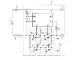
- This battery pack includes a secondary battery 1 and a protection circuit 2.
- the protection circuit 2 is connected to the cell positive terminal 3 and the cell negative terminal 4 of the secondary battery 1, and discharges from the secondary battery 1 to an external load or from the outside via the positive output terminal 5 and the negative output terminal 6.
- the secondary battery 1 is charged.
- a PTC element 7 and a charge / discharge control switch 8 are inserted in the charge / discharge path on the negative electrode side connecting the cell negative electrode terminal 4 and the negative electrode output terminal 6.
- the PTC element 7 is used as a temperature protection element, and restricts or cuts off the current flowing through the charging / discharging path according to a change in resistance value according to a temperature rise due to heat generation of the secondary battery 1.
- the charge / discharge control switch 8 is composed of two switch circuits 8a and 8b connected in parallel. Each of the switch circuits 8a and 8b is configured by connecting a discharge control FET 9a made of a MOSFET and a charge control FET 10a in series.
- the discharge control FET 9a is connected so that the parasitic diode 9b existing between the drain and the source is in a forward direction with respect to the charging current flowing from the positive electrode output terminal 5 toward the secondary battery 1.
- the charge control FET 10a is connected such that the parasitic diode 10b is in the forward direction with respect to the discharge current.
- the power supply voltage is supplied from the secondary battery 1 to the power supply terminal VDD via the resistor R ⁇ b> 1 and the capacitor C.
- the reference potential terminal VSS is connected to the secondary battery 1 side of the charge / discharge control switch 8. Further, the overcurrent detection terminal V ⁇ is connected to the negative output terminal 6 side of the charge / discharge control switch 8 through the resistor R2.
- Control signals DO and CO from the protection IC 11 are supplied to the gates of the discharge control FET 9a and the charge control FET 10a, respectively.
- the control signals DO and CO are set to the high level, and the discharge control FET 9a and the charge control FET 10a are controlled to be in the ON state.
- the protection IC 11 detects the voltage between the reference potential terminal VSS and the overcurrent detection terminal V ⁇ , and detects the current flowing through the charge / discharge path equivalently from the detected voltage. That is, the current is equivalently detected based on the voltage drop caused by the ON resistance of the discharge control FET 9a and the charge control FET 10a. When a current exceeding a specified current value (that is, overcurrent) flows, the discharge control FET 9a or the charge control FET 10a is turned off to cut off the current.
- An improvement that facilitates quick charging of the secondary battery is desired for the secondary battery pack having the above-described configuration.
- One of the reasons is that a higher capacity is particularly demanded for lithium secondary batteries as the functions of mobile phones and the like increase.
- the time required for charging becomes longer than the practical range.
- it is required to enable charging with a larger current value, to shorten the time required for charging, that is, to enable rapid charging.
- it is necessary to reduce the impedance of the secondary battery pack.
- Examples of improvements to reduce the impedance of the secondary battery pack include the protection circuit 2, the PTC element 7 (temperature protection element), and the specific resistance of the wiring material.
- configuring the charge / discharge control switch 8 by connecting two switch circuits 8 a and 8 b in parallel is one of the measures for reducing the resistance of the protection circuit 2. That is, the charge / discharge control switch 8 can basically be constituted by one switch circuit. In contrast, the on-resistance of the charge / discharge control switch 8 can be reduced by connecting the two switch circuits 8a and 8b in parallel.
- the overcurrent protection operation will not work unless a current of 5.5 to 8.3 times flows. There is concern about a decrease in safety. Accordingly, it is desirable that the resistance values of the discharge control FET 9a and the charge control FET 10a be about 8 m ⁇ to 10 m ⁇ (protection current value setting about 3 times the 1C capacitance value). Accordingly, it is desirable to limit the number of MOSFETs connected in parallel to two, including the viewpoint of cost and mounting area.
- the resistance value of the PTC element 7 is about 0.005 ⁇ , it is generally possible to reduce the resistance of the element portion by using a breaker (about 2.5 m ⁇ ) instead of the PTC element.
- a breaker about 2.5 m ⁇
- the impedance of the secondary battery pack it remains to reduce the resistance of the wiring material connecting the secondary battery and the protection circuit, the secondary battery and the breaker, and the breaker and the protection circuit.
- pure Ni is used for the wiring material from the viewpoint of weldability.
- the conductivity is improved as compared with conventional Ni, so that connection by welding is difficult.
- Lead material (wiring material) is used.
- the battery lead material is disposed between the battery electrode and the external terminal of the battery pack, and the weld layer is fixedly connected to the electrode by resistance welding.
- the electrical resistance can be reduced by about half compared to the conventional lead material using pure nickel, and the corrosion resistance and weldability are also excellent.
- Patent Document 2 discloses a battery pack in which positive and negative terminals of a battery and a protective circuit board are connected to each other by a wiring material.
- a wiring material it is described that a clad plate made of a dissimilar metal obtained by bonding an aluminum plate having a bonding property to a battery terminal and a nickel plate having a bonding property to a protective circuit board is described.
- the protective circuit board can be connected with a short wiring material disposed on the same side surface of the battery, the length of the wiring material can be shortened, the cost of the battery pack can be reduced, and the manufacturing process can be simplified. It is described.
- one of the metal plates is made of a low-resistance metal such as aluminum or copper as the dissimilar metal clad, the impedance of the wiring material can be lowered.
- JP 11-297300 A Japanese Patent Laid-Open No. 2002-289160
- Patent Document 1 discloses a structure in which a Cu-Ni clad material is used and a Ni layer suitable for welding is welded to the battery electrode and the protection circuit electrode.
- Patent Document 1 does not describe a connection form between the battery electrode and the protection circuit board.
- Patent Document 2 discloses that a clad plate made of a different metal is used as a wiring material for connection between a battery electrode and a protection circuit board. That is, a clad plate is used in which a first metal plate having bonding properties to battery electrodes and a second metal plate having bonding properties to terminals of the protection circuit board are bonded together. Further, it is disclosed that as a clad material using Cu, Cu is used as a first metal plate and Al is used as a second metal plate.
- Patent Document 2 uses a clad plate obtained by bonding a first metal plate having bonding properties to battery electrodes and a second metal plate having bonding properties to terminals of the protection circuit board. Different metal layers are welded to the electrode of the battery and the terminal of the protection circuit board. Therefore, in the case of the clad material using Cu, the Cu material becomes the surface on one side of the welded portion, and there arises a problem that burns and cracks occur due to series welding.
- the wiring material specifically described as an embodiment in Patent Document 2 is an Al—Ni clad material. For this reason, there is no description about the problem recognition and the solution to the problem of burning and cracks generated in the Cu layer when using a Cu—Ni clad material.
- the present invention provides a secondary battery pack in which a Cu—Ni clad material is used as a wiring material between a battery electrode and a protection circuit board to reduce resistance and to solve the problem of burning the Cu material.
- the purpose is to do.
- the secondary battery pack of the present invention includes, as a basic configuration, a secondary battery, and a protection circuit disposed in a charge / discharge path between a pair of cell electrode terminals of the secondary battery and an external output terminal,
- the protection circuit includes a charge / discharge control switch inserted in series in the charge / discharge path, and a current detection unit that detects a current flowing through the charge / discharge path, and a detection value of the current detection unit reaches an overcurrent region.
- the charge / discharge control switch is configured to be turned off, and a protection circuit board on which the protection circuit is mounted is mounted to face the cell electrode terminal of the secondary battery.
- the secondary battery pack of the present invention includes a Ni layer as a wiring material for connecting between each of the pair of cell electrode terminals of the secondary battery and the circuit terminals of the protection circuit board. And a Cu—Ni clad material comprising a Cu layer or a Cu alloy layer, and the wiring material is joined by resistance welding with the Cu electrode side abutting against the cell electrode terminal and the circuit terminal. It is characterized by being.
- the resistance of the wiring portion of the secondary battery pack can be reduced by using the Cu—Ni clad material as the wiring material.
- the wiring material is bonded by resistance welding with the Cu layer side being brought into contact with the cell electrode terminal and the circuit terminal, the occurrence of the problem of burning the Cu material is avoided. Therefore, it is possible to further reduce the resistance of the wiring part of the secondary battery pack without deteriorating the joint strength of the connection part by resistance welding. As a result, it is possible to improve the ease of rapid charging at a high current for a secondary battery pack having a configuration in which a protection circuit is connected to the secondary battery.
- FIG. 1 is a block diagram showing a circuit configuration of a secondary battery pack according to an embodiment of the present invention.
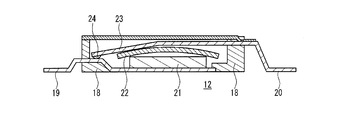
- FIG. 2 is a cross-sectional view showing a configuration of a breaker that is an element of the secondary battery pack
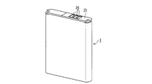
- FIG. 3 is a perspective view showing an appearance of the secondary battery pack.
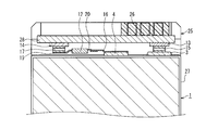
- FIG. 4 is a cross-sectional view of a principal part conceptually showing a mounting portion of the protective circuit board 28 for the secondary battery 1.
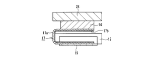
- 5 is a partial cross-sectional view showing an enlarged connection portion between the cell positive electrode terminal 3 and the protection circuit board 28 of the secondary battery 1 as viewed from the right side in FIG.
- FIG. 6 is an enlarged partial cross-sectional view showing a connection portion between the cell negative electrode terminal 4 and the breaker 12 of the secondary battery 1 when viewed from the front in FIG. 7 is an enlarged partial cross-sectional view showing a connection portion between the breaker 12 and the protection circuit board 28 as viewed from the left side in FIG.
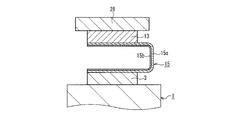
- FIG. 8 is a cross-sectional view showing the operation when the positive terminal 3 and the wiring member 15 are series-welded.
- FIG. 9 is a cross-sectional view showing the operation when the lead terminal 19 and the wiring member 16 are directly welded.
- FIG. 10 is a cross-sectional view showing problems when series welding is performed with the Ni layer 15b in contact with the cell positive and negative electrode terminals 3.
- FIG. 11 is a block diagram showing a conventional secondary battery pack.
- the secondary battery pack of the present invention can take the following aspects based on the above configuration.
- the wiring member connecting between the circuit terminal and the cell electrode terminal is bent at an angle of 180 degrees in a U shape with the Ni layer inside, forming upper and lower bent pieces. Then, the upper bent piece and the lower bent piece can be configured such that the Cu layer faces the circuit terminal and the cell electrode terminal, respectively.
- FIG. 1 is a block diagram showing a circuit configuration of a secondary battery pack according to an embodiment of the present invention. Constituent elements similar to those of the conventional example shown in FIG. 11 are denoted by the same reference numerals, and the repeated description is simplified.
- the secondary battery pack includes a secondary battery 1 such as a lithium ion battery.
- a protection circuit 2 is connected to the secondary battery 1, and discharging to an external load or charging from the outside is performed via a positive electrode (external) output terminal 5 and a negative electrode (external) output terminal 6 of the protection circuit 2. Is called.
- a charge / discharge control switch 8 comprising a breaker 12 and two switch circuits 8a, 8b connected in parallel.
- the breaker 12 has a configuration in which a bimetal and a PTC element are combined, and a specific structure and operation thereof will be described later, but is used in place of the PTC element 7 in the conventional example shown in FIG.
- FIG. 1 shows a wiring material 15 that connects the cell positive terminal 3 of the secondary battery 1 and the circuit terminal 13 of the protection circuit 2, a wiring material 16 that connects the cell negative terminal 4 of the secondary battery 1 and the breaker 12, and a breaker.
- the wiring material 17 which connects 12 and the circuit terminal 14 of the protection circuit 2 is shown.
- a Cu—Ni clad material (having a Ni layer only on one side) made of a Ni layer and a Cu layer or a Cu alloy layer is used as the wiring material 15, the wiring material 16, and the wiring material 17. .
- a feature of this embodiment is that the Cu layer side of the Cu—Ni clad material of the wiring materials 15 to 17 is joined to the cell positive and negative electrode terminals 3 and 4 and the circuit terminals 13 and 14 by resistance welding. It is. Details and effects of this configuration will be described later.
- Breaker 12 has a structure shown in a sectional view in FIG. That is, the lead terminals 19 and 20 are supported by the frame 18, and the PTC element 21 and the bimetal 22 are disposed between them. The outer ends of the lead terminals 19 and 20 protruding outside the frame 18 are connected to the charge / discharge path as shown in FIG.
- the inner end portion of the lead terminal 19 is disposed at the bottom, and the inner end portion of the lead terminal 20 is disposed at the upper portion and faces in the vertical direction.
- a bent portion 23 is formed at the end of the lead terminal 20 in the frame 18, and a terminal protrusion 24 is provided at the tip thereof. Due to the action of the PTC element 21 and the bimetal 22 disposed between both inner end portions, the conduction form between the lead terminals 19 and 20 changes according to the temperature.
- the first conduction state is a state in which the lead terminals 19 and 20 are directly conducted by the terminal protrusion 24 coming into contact with the lead terminal 19. This state is formed by the bimetal 22 being bent so as to protrude upward as shown in the drawing.
- the lead terminals 19 and 20 are in a second conduction state in which the lead terminals 19 and 20 are indirectly conducted via the PTC element 21 and the bimetal 22. In this state, the resistance is extremely high, and the current is substantially cut off, but some current flows.
- the breaker 12 in the first conduction state, since a current flows by direct conduction between the lead terminals 19 and 20, the breaker 12 is in an extremely low resistance state. Since the breaker 12 has a mechanical contact structure, there is no resistance fluctuation in the temperature range until the bimetal is reversed. That is, the resistance value does not depend on temperature, and a stable low resistance can be realized as compared with the PTC element 7 whose resistance value varies depending on the temperature. In rapid charging in which charging is performed with a large current, the heat generation of the cell increases. Therefore, a breaker that is not subjected to a resistance change due to the heat generation of the cell during charging is an element advantageous in reducing the resistance.
- the temperature protection element means an element having a function of limiting the current flowing through the charge / discharge path according to the temperature rise due to heat generation of the secondary battery 1.
- the charge / discharge control switch 8 including the two switch circuits 8a and 8b connected in parallel. That is, even if the present invention is applied to the case where the charge / discharge control switch 8 is configured by a series circuit of a single discharge control FET 9a and a charge control FET 10a, a corresponding effect can be obtained.
- FIG. 3 is a perspective view showing an appearance of the secondary battery pack according to the present embodiment.
- a cap frame 25 is attached to the upper part of the secondary battery 1.
- a protective circuit board is attached to the upper part of the inside, but it does not appear in FIG. 3 because it is covered with a cover material.
- a protection circuit 2 including a protection IC 11 and the like is mounted on the protection circuit board.
- An output terminal 26 for external connection is exposed from the upper end surface of the cap frame 25.
- the output terminal 26 is attached to the protection circuit board and includes the positive output terminal 5 and the negative output terminal 6 of FIG.
- FIG. 4 is a principal cross-sectional view conceptually showing a mounting portion of the protective circuit board for the secondary battery 1, and shows a cross-sectional structure of the secondary battery pack from which the cover material is removed from the state of FIG.
- the secondary battery 1 is configured by incorporating a unit cell inside an outer can 27 made of, for example, aluminum or an aluminum alloy. Since the internal configuration of the outer can 27 is general, the illustration is omitted.
- the cell positive electrode terminal 3 and the cell negative electrode terminal 4 arranged on the upper surface portion of the outer can 27 are electrically connected to the positive electrode and the negative electrode of the unit cell, respectively.
- the cell positive electrode terminal 3 may be composed of a clad plate.
- the cap frame 25 is mounted on the top of the outer can 27 and forms a space between the upper surface of the outer can 27.
- a protection circuit board 28 is mounted so as to be positioned above the space.
- the protection circuit 2 is mounted on the protection circuit board 28.
- the circuit terminal 13 provided on the lower surface of the protection circuit board 28 is connected to the cell positive terminal 3 by the wiring material 15.
- the similarly provided circuit terminal 14 is connected to the cell negative electrode terminal 4 by the wiring members 16 and 17 with the breaker 12 interposed.
- FIGS. 5 to 7 are partial cross-sectional views showing enlarged connection portions by the wiring members 15 to 17.
- FIG. 5 is a view as seen from the right side of FIG. 4 and shows a connection portion between the cell positive terminal 3 of the secondary battery 1 and the circuit terminal 13 of the protection circuit 2.
- FIG. 6 is a view as seen from the front of FIG. 4 and shows a connection portion between the cell negative electrode terminal 4 of the secondary battery 1 and the lead terminal 20 of the breaker 12.
- FIG. 7 is a view seen from the left side of FIG. 4 and shows a connection portion between the circuit terminal 14 of the protection circuit 2 and the lead terminal 19 of the breaker 12.
- FIG. 4 is conceptually shown for easy viewing, it does not correspond to the dimensions of the respective parts in FIGS.
- the secondary battery 1, the breaker 12, and the protection circuit board 28 in this configuration are connected as follows by welding with the wiring members 15 to 17. That is, as shown in FIG. 5, one end of the wiring member 15 and the circuit terminal 13 of the protection circuit board 28, and the other end of the wiring member 15 and the cell positive electrode terminal 3 of the secondary battery 1 are joined by welding. Yes.
- the wiring material 15 is a clad material composed of a Cu layer 15a and a Ni layer 15b, and is bent in a U-shape, that is, at an angle of 180 degrees with the Ni layer 15b on the inside. Accordingly, the wiring member 15 forms upper and lower bent pieces, and the Cu layer 15a faces upward in the upper bent piece, and the Cu layer 15a faces downward in the lower bent piece. Thus, the wiring member 15 is welded with the Cu layer 15a facing both the cell positive electrode terminal 3 and the circuit terminal 13.
- the wiring material 16 is also a clad material composed of the Cu layer 16a and the Ni layer 16b, and is resistance-welded with the Cu layer 16a facing the cell negative electrode terminal 4 by placing the Cu layer 16a on the lower side.
- the Cu layer 16a is opposed to the lead terminal 20
- the Ni layer 16b may be opposed to the lead terminal 20 as described later.
- the wiring material 17 is also a clad material composed of the Cu layer 17a and the Ni layer 17b, and is bent in a U shape with the Ni layer 17b inside, that is, at an angle of 180 degrees.
- the circuit layer 14 is welded with the Cu layer 17a facing the circuit terminal 14.
- the Cu layer 16a is also opposed to the lead terminal 19
- the Ni layer 16b may be opposed to the lead terminal 20 as in the case of the lead terminal 20.
- the wiring members 15 to 17 are resistance-welded to the cell positive and negative terminals 3 and 4 and the circuit terminals 13 and 14 with the Cu layers 15a to 17a facing each other. Therefore, even if the joining using the conventional resistance welding technique is applied, it is possible to avoid the Cu material from being burned and the Cu material from being cracked. Therefore, the resistance of the wiring part of the secondary battery pack can be further reduced without deteriorating the characteristics of the connection part by welding. As a result, it is possible to improve the ease of rapid charging at a high current for a secondary battery pack having a configuration in which a protection circuit is connected to the secondary battery.
- series welding is used for welding the wiring members 15 to 17 to the cell positive and negative terminals 3 and 4 and the circuit terminals 13 and 14 for the reason described later.
- direct welding can be used for welding the wiring members 16 and 17 to the lead terminals 19 and 20 of the breaker 12.
- FIG. 8 shows the action accompanying series welding in the case of the cell positive electrode terminal 3 and the wiring material 15 as an example.
- FIG. 9 shows the effects of direct welding in the case of the lead terminal 19 and the wiring member 16 as an example.
- the series welding as shown in FIG. 8
- two electrode rods 29 are pressed against the same plane on the upper part of the wiring member 15 brought into contact with the cell positive and negative electrode terminals 3 to energize.
- direct welding as shown in FIG. 9, the electrode rod 29 is pressed against the lower surface of the lead terminal 19 and the upper surface of the wiring member 16 in an opposing direction to energize.
- a welding point 30 is formed between the cell positive / negative electrode terminal 3 and the wiring member 15 by the effective current Ie flowing through the cell positive / negative electrode terminal 3 as shown in FIG.
- reactive currents In and Ic flowing in the Ni layer 15b and the Cu layer 15a are also generated, but these do not contribute to welding.
- the metal burns due to the reactive currents In and Ic flowing in a place different from the point where the welding is originally desired.
- the Ni layer 15b is disposed on the upper portion, the reactive current on the surface layer is suppressed, and the influence of burning or the like is small.
- the action when series welding is performed with the Ni layer 15b in contact with the cell positive and negative electrode terminals 3 is shown in FIG.
- the reactive current Ic flowing through the Cu layer 15a with which the electrode rod 29 abuts is large due to the low resistance of Cu. Therefore, heat may be generated even between the electrode rod 29 and the Cu layer 15a, and an unnecessary welded portion 32 of the electrode rod 29 to the Cu layer 15a may be formed. If the electrode rod 29 is forcibly separated in this state, a part of the Cu layer 15a may adhere to the electrode rod 29 and peel off. As a result, the Cu layer 15a becomes thin, and as a result, cracks occur.
- the electrode rod 29 is arranged in contact with the Ni layer 15b. Accordingly, the reactive current on the surface layer is suppressed, and the joining of the Ni layer 15b to the electrode rod 29 can be substantially avoided. Furthermore, since the Ni layer is harder than the Cu layer, even if the electrode rod is joined, a part of Ni does not adhere to the electrode rod and is not easily peeled off.
- FIG. 9 shows a structure in which the Cu layer 15a is in contact with the lead terminal 19, but there is no problem if resistance welding is performed with the Ni layer 15b in contact.
- connection process among the secondary battery 1, the breaker 12, and the protection circuit board 28 in this configuration can be performed as follows as an example.
- the wiring members 15 and 17 are initially flat and are used with the Ni layers 15b and 17b facing upward, and are bent into a U shape in a later step.
- the Cu layer 17a or Ni layer 17b at one end of the wiring member 17 is brought into contact with the lead terminal 19 of the breaker 12 and joined by direct welding.
- the Cu layer 16a or Ni layer 16a at one end of the wiring member 16 is brought into contact with the lead terminal 20 of the breaker 12 and joined by direct welding.
- the protection circuit board 28 is placed in an upside down posture with respect to the state shown in FIG. And the Cu layer 15a of the one end part of the wiring material 15 is contact
- the upper end surface (the lower end surface in FIG. 4) of the protection circuit board 28 in the state of being inverted upside down as described above and the upper end surface of the secondary battery 1 are aligned.
- the circuit terminals 13 and 14 of the protection circuit board 28, and the cell positive terminal 3 and the cell negative terminal 4 of the secondary battery 1 are aligned on the same plane.
- the Cu layer 15a at the other end of the wiring member 15 is brought into contact with the cell positive terminal 3 of the secondary battery 1, and the Cu layer 16a at the other end of the wiring member 16 is brought into contact with the cell negative terminal 4. And each is joined by series welding. Thereafter, the wiring members 15 and 17 are bent by 180 degrees at the center as shown in FIGS. 5 and 7, so that the protective circuit board 28 is mounted on the outer can 27 as shown in FIG. State. By holding this state, the mounting is completed.
- cap frame 25 and the outer can 27 are integrated by injecting an integrally molded resin into the space between the cap frame 25 and the outer can 27, and the secondary battery 1 is completed.
- a configuration in which the cap frame itself is formed of an integrally molded resin, a configuration in which a protection circuit or the like is mounted on the inner frame, and the secondary battery is formed by covering with the cap frame may be used.
- the secondary battery pack of the present invention can reduce the impedance of the secondary battery pack by using a Cu—Ni clad material as a wiring material, and can avoid the problems associated with welding. It is useful as a battery pack used for a device such as a telephone that is required to be rapidly rechargeable.
Landscapes
- Chemical & Material Sciences (AREA)
- Chemical Kinetics & Catalysis (AREA)
- Electrochemistry (AREA)
- General Chemical & Material Sciences (AREA)
- Engineering & Computer Science (AREA)
- Mechanical Engineering (AREA)
- Power Engineering (AREA)
- Microelectronics & Electronic Packaging (AREA)
- Manufacturing & Machinery (AREA)
- Battery Mounting, Suspending (AREA)
- Secondary Cells (AREA)
Abstract
二次電池(1)と、二次電池のセル電極端子(3, 4)と外部出力端子(5, 6)の間の充放電路中に配置された保護回路(2)とを備えた二次電池パック。保護回路は、充放電路に直列に挿入された充放電制御スイッチ(8)と、充放電路を流れる電流を検出する電流検出部を有し、電流検出部の検出値が過電流域に達したときに、充放電制御スイッチをオフに制御する。保護回路が実装された保護回路基板が、二次電池のセル電極端子と対向して装着される。二次電池のセル電極端子の各々と、保護回路基板の回路端子の間を接続する配線材(15,16,17)として、Ni層とCu層またはCu合金層からなるCu-Niクラッド材が用いられ、配線材は、セル電極端子及び回路端子に対してCu層側を当接させて溶接されている。電池の電極と保護回路基板との間の配線材として、低抵抗化のためにCu-Niクラッド材を用いた場合の、抵抗溶接に伴うCu材の焼けの発生が解消される。
Description
本発明は、二次電池に保護回路が接続された二次電池パックに関し、特に、高電流による急速充電を容易とするためにインピーダンスが低減された二次電池パックに関する。
電池パックは、内蔵された二次電池の正負極に接続された外部出力端子から外部へ通電可能な状態で提供される。また、過充電、過放電、過大電流、異常な温度上昇等の異常状態から二次電池を保護するために、異常状態が発生したときには充放電を停止する制御を行う保護機能を有する。すなわち、外部出力端子と二次電池との間に充放電制御スイッチを介在させて、保護回路により充放電制御スイッチを制御する。保護回路は、過充電、過放電等が検出されたときに、充放電制御スイッチをオフにして充放電路を遮断する制御を行い、二次電池を保護する。
図11は、そのような保護機能を有する二次電池パックの従来例を示す。この電池パックは、二次電池1と、保護回路2から構成される。保護回路2は、二次電池1のセル正極端子3及びセル負極端子4に接続され、正極出力端子5及び負極出力端子6を介して、二次電池1から外部負荷への放電、あるいは外部からの二次電池1に対する充電が行われる。
セル負極端子4と負極出力端子6とを結ぶ負極側の充放電路中には、PTC素子7と、充放電制御スイッチ8が挿入されている。PTC素子7は温度保護素子として用いられ、二次電池1の発熱による昇温に応じた抵抗値の変化により、充放電路を流れる電流を制限し、あるいは遮断する。
充放電制御スイッチ8は、並列接続された2つのスイッチ回路8a、8bにより構成されている。スイッチ回路8a、8bは各々、MOSFETからなる放電制御FET9a、及び充電制御FET10aを直列に接続して構成されている。放電制御FET9aは、ドレイン・ソース間に存在する寄生ダイオード9bが、正極出力端子5から二次電池1の方向に流れる充電電流に対して順方向となるように接続されている。充電制御FET10aは、寄生ダイオード10bが、放電電流に対して順方向となるように接続されている。
保護IC11により構成された電圧監視部では、二次電池1から、抵抗R1、キャパシタCを介して、電源電圧が電源端子VDDに供給される。基準電位端子VSSは、充放電制御スイッチ8の二次電池1の側に接続されている。また、過電流検出端子V-は、抵抗R2を介して、充放電制御スイッチ8の負極出力端子6の側に接続されている。
放電制御FET9aおよび充電制御FET10aのそれぞれのゲートには、保護IC11からの制御信号DOおよびCOがそれぞれ供給される。通常の充電および放電動作では、制御信号DOおよびCOがハイレベルとされ、放電制御FET9aおよび充電制御FET10aがON状態に制御される。
保護IC11は、基準電位端子VSSと過電流検出端子V-の間の電圧を検出し、検出された電圧から、等価的に充放電路に流れる電流を検出する。すなわち、放電制御FET9aおよび充電制御FET10aのオン抵抗によって生じる電圧降下に基づいて等価的に電流を検出する。規定の電流値以上の電流(すなわち、過電流)が流れた場合に、放電制御FET9aまたは充電制御FET10aをOFFさせて電流を遮断する。
以上のような構成の二次電池パックに対して、二次電池の急速充電を容易とする改良が望まれている。その理由の一つは、携帯電話などの高機能化に伴って、特に、リチウム二次電池にはより高容量が求められていることである。高容量化に伴い、従来と同程度の電流値による充電では、充電に要する時間が実用的な範囲を超えて長くなる。これを回避するためには、より大きな電流値での充電を可能として、充電に要する時間を短縮化すること、すなわち急速充電を可能とすることが求められる。大電流での充電を可能とするためには、二次電池パックのインピーダンスを低減することが必要である。二次電池パックの低インピーダンス化の改良対象としては、保護回路2、PTC素子7(温度保護素子)、配線材の固有抵抗が挙げられる。
図11のように、2つのスイッチ回路8a、8bを並列接続して充放電制御スイッチ8を構成することは、保護回路2の抵抗を低減するための方策の一つである。すなわち、充放電制御スイッチ8は、基本的には1個のスイッチ回路で構成することができる。これに対して、2つのスイッチ回路8a、8bを並列接続することにより、充放電制御スイッチ8のオン抵抗を低減することができる。
しかし、このように構成された充放電制御スイッチ8を通して電流が流れた場合、各々の放電制御FET9aおよび充電制御FET10aのオン抵抗によって生じる電圧降下は少なくなる。従って、充放電路に流れる電流として等価的に検出される値は小さくなり、過大電流として検出できる電流レベルが高くならざるを得ない。すなわち、保護ICの過大電流検出値の一般的な最小値は0.05Vであるため、充放電制御スイッチ8のオン抵抗を、例えば0.003Ωまで低減させた場合、過大電流として検出できる電流値が0.05V÷0.003Ω=16.6Aとなってしまう。
そのため、一般的なモバイル機器に用いるリチウムイオン電池の容量帯域(2Ah~3Ah)においては、5.5倍~8.3倍の電流が流れた場合でなければ過大電流保護動作が働かないこととなり、安全性の低下が懸念される。従って、放電制御FET9aおよび充電制御FET10aの抵抗値は8mΩ~10mΩ程度(1C容量値の約3倍の保護電流値設定)にする事が望ましい。従って、コスト、実装面積からの観点も含めて、並列接続するMOSFETは、2個に留める事が望ましい。
また、PTC素子7の抵抗値は約0.005Ωであるため、PTC素子に代えてブレーカー(約2.5mΩ)を用いることで、当該素子部分の低抵抗化が可能であることが一般的に知られている。従って、二次電池パックのインピーダンスを更に低減するためには、二次電池と保護回路、二次電池とブレーカー、及びブレーカーと保護回路を接続する配線材の低抵抗化を図ることが、残された課題として挙げられる。従来は、溶接性の観点から、配線材に純Niが用いられている。これに対し、Cu材を用いて配線材の低インピーダンス化を図ることが知られている。しかし、Cu材を用いる場合、導電率が従来のNiに比べて向上するため、溶接による接続が困難である。
そこで、特許文献1に開示された技術では、電極に溶接接続するためのNi、Ni合金またはFe合金からなる溶接層と、Cu又は耐熱Cu合金からなる基層とがクラッドされた2層構造の電池用リード材料(配線材)を用いる。この電池用リード材料が、電池の電極と電池パックの外部端子間に配置され、抵抗溶接により溶接層が電極へ固着接続されている。これにより、純ニッケルを使用した従来のリード材料に比べて、電気抵抗を約半分に低減することができ、かつ耐食性・溶接性にもすぐれている、とされている。
また、特許文献2には、電池の正負極の端子と保護回路基板とを配線材によりそれぞれ接続した電池パックが開示されている。配線材としては、電池の端子に対して接合性を有するアルミニウム板と、保護回路基板に対して接合性を有するニッケル板とを貼り合わせた異種金属のクラッド板を用いることが記載されている。これにより、保護回路基板を電池の同一側面に配置された短い配線材で接続できるので、配線材の長さを短縮でき、電池パックのコスト低減、及び製造工程の簡素化を図ることができる、と記載されている。さらに、異種金属のクラッドとして金属板の一方をアルミニウムや銅のような低抵抗の金属から構成すれば、配線材のインピーダンスを下げることが可能になる、と記載されている。
二次電池、保護回路、及びブレーカーを相互に接続するクラッド材としては、低抵抗の観点から、Ni層と、Cu層またはCu合金層とからなるCu-Niクラッド材を用いることが望ましい。これに関し、特許文献1には、Cu-Niクラッド材を用い、溶接に適したNi層を電池の電極と保護回路の電極に対して溶接させた構造が開示されている。
ところが、Cu-Niクラッド材を用い、溶接に適したNi層を電極に当接させて抵抗溶接を行う実験を行った結果、抵抗溶接のシリーズ溶接ではCu材が焼ける事や、Cu材に亀裂が生じて、配線材としての機能が劣化することが判った。また、特許文献1には、電池の電極と保護回路基板との接続形態に関する記載はない。
一方、特許文献2には、電池の電極と保護回路基板との接続のための配線材として、異種金属のクラッド板を用いることが開示されている。すなわち、電池の電極に対して接合性を有する第1の金属板と、保護回路基板の端子に対して接合性を有する第2の金属板を貼り合わせたクラッド板を用いる。また、Cuを用いたクラッド材として、第1の金属板としてCuを用い、第2の金属板としてAlを用いることが開示されている。
しかし、特許文献2では、電池の電極に対して接合性を有する第1の金属板と、保護回路基板の端子に対して接合性を有する第2の金属板を貼り合わせたクラッド板を用いるため、電池の電極と保護回路基板の端子には各々異なる金属層が溶接される。従って、Cuを用いたクラッド材の場合、溶接部の一方では、Cu材が表面になり、シリーズ溶接によって焼けや亀裂が生じる問題が発生する。
また、特許文献2に実施の形態として具体的に記載された配線材は、Al-Niクラッド材である。このため、Cu-Niクラッド材を用いた場合の、Cu層に発生する焼けや亀裂の問題に対する課題認識、および解決策に関する記載はない。
従って、本発明は、電池の電極と保護回路基板との間の配線材としてCu-Niクラッド材を用いて低抵抗化を図り、それに伴うCu材が焼ける問題を解消した二次電池パックを提供することを目的とする。
本発明の二次電池パックは基本構成として、二次電池と、前記二次電池の一対のセル電極端子と外部出力端子との間の充放電路中に配置された保護回路とを備え、前記保護回路は、前記充放電路に直列に挿入された充放電制御スイッチと、前記充放電路を流れる電流を検出する電流検出部を有し、前記電流検出部の検出値が過電流域に達したときに、前記充放電制御スイッチをオフに制御するように構成され、前記保護回路が実装された保護回路基板が、前記二次電池の前記セル電極端子と対向して装着されている。
上記課題を解決するために、本発明の二次電池パックは、前記二次電池の前記一対のセル電極端子の各々と、前記保護回路基板の回路端子の間を接続する配線材として、Ni層と、Cu層またはCu合金層とからなるCu-Niクラッド材が用いられ、前記配線材は、前記セル電極端子及び前記回路端子に対してCu層側を当接させて抵抗溶接により接合されていることを特徴とする。
上記構成の二次電池パックによれば、配線材にCu-Niクラッド材を用いることで、二次電池パックの配線部の抵抗を低減させることができる。しかも、配線材は、セル電極端子及び回路端子に対してCu層側を当接させて抵抗溶接により接合されているので、Cu材が焼ける問題の発生が回避されている。従って、抵抗溶接による接続部の接合強度を劣化させることなく、二次電池パックの配線部の抵抗をより低減させることが可能である。この結果、二次電池に保護回路が接続された構成の二次電池パックに対する、高電流での急速充電の容易性を向上させることができる。
本発明の二次電池パックは、上記構成を基本として、以下のような態様をとることができる。
すなわち、前記回路端子と前記セル電極端子との間を接続する前記配線材は、前記Ni層を内側にしてU字状に180度の角度で屈曲されて、上側及び下側の屈曲片を形成し、上側の屈曲片及び下側の屈曲片が各々、前記回路端子及び前記セル電極端子に対してCu層を対向させている構成とすることができる。
以下、本発明の実施形態について図面を参照しながら説明する。
<実施の形態>
図1は、本発明の一実施の形態における二次電池パックの回路構成を示すブロック図である。図11に示した従来例と同様の構成要素については同一の参照符号を付して、説明の繰り返しを簡略化する。
図1は、本発明の一実施の形態における二次電池パックの回路構成を示すブロック図である。図11に示した従来例と同様の構成要素については同一の参照符号を付して、説明の繰り返しを簡略化する。
この二次電池パックは、例えば、リチウムイオン電池等の二次電池1を内蔵している。二次電池1には保護回路2が接続され、保護回路2の正極(外部)出力端子5及び負極(外部)出力端子6を介して、外部の負荷への放電、あるいは外部からの充電が行われる。
二次電池1のセル負極端子4と、負極出力端子6の間の負極側の充放電路中には、ブレーカー12と、2つの並列接続されたスイッチ回路8a、8bからなる充放電制御スイッチ8が、直列に接続されている。ブレーカー12は、バイメタルとPTC素子を組み合わせた構成を有し、その具体的な構造及び動作については後述するが、図11に示した従来例におけるPTC素子7に代えて用いられている。
図1には、二次電池1のセル正極端子3と保護回路2の回路端子13を接続する配線材15、二次電池1のセル負極端子4とブレーカー12を接続する配線材16、及びブレーカー12と保護回路2の回路端子14を接続する配線材17が示されている。本実施の形態では、配線材15、配線材16、及び配線材17として、Ni層と、Cu層またはCu合金層とからなるCu-Niクラッド材(片側のみにNi層を有する)が用いられる。
本実施の形態の特徴は、セル正負極端子3、4、及び回路端子13、14に対して、抵抗溶接により、配線材15~17のCu-Niクラッド材のCu層側が接合されていることである。この構成の詳細及び効果については、後述する。
ブレーカー12は、図2に断面図で示す構造を有する。すなわち、枠体18にリード端子19、20が支持され、それらの間に、PTC素子21及びバイメタル22が配置されている。枠体18の外部に突出したリード端子19、20の外端部が、図1に示したように充放電路中に接続される。
枠体18内で、リード端子19の内端部は底部に配置され、リード端子20の内端部は上部に配置されて上下方向に対向する。枠体18内のリード端子20の端部には屈曲部23が形成され、その先端に端子突起24が設けられている。両内端部間に配置されたPTC素子21及びバイメタル22の作用により、リード端子19、20間の導通形態が温度に応じて変化する。第1導通状態は、端子突起24がリード端子19に当接することにより、リード端子19、20間が直接導通した状態である。この状態は、常温下でバイメタル22が、図示されるように上方に凸となるように湾曲していることによって形成される。
一方、温度が上昇したときには、湾曲の程度が小さく(曲率が小さく)なり、リード端子20の屈曲部23が上方に反り返って端部が上方に変位する。それにより、端子突起24はリード端子19から離間して、端子突起24を介した電流経路は遮断される。そのため、リード端子19、20間は、PTC素子21及びバイメタル22を介して間接的に導通した第2導通状態となる。この状態では、極めて高抵抗であり、実質的に電流は遮断されるが、若干の電流は流れる。
以上のとおり、第1導通状態では、リード端子19、20間の直接導通によって電流が流れるので、ブレーカー12は極めて低抵抗の状態である。ブレーカー12は機械的接点構造の為、バイメタルが反転するまでの温度帯においては抵抗変動がない。つまり、抵抗値の温度依存性がなく、温度によって抵抗値が変動するPTC素子7と比べて安定した低抵抗を実現できる。大電流で充電する急速充電においては、セルの発熱が増すため、充電時のセルの発熱による抵抗変化をうけないブレーカーは、低抵抗化に有利な素子である。
但し、本発明は、ブレーカー12ではなく、例えば温度ヒューズ等の他の温度保護素子を用いた場合に適用しても、相応の効果を得ることが可能である。なお、温度保護素子とは、二次電池1の発熱による昇温に応じて、充放電路を流れる電流を制限する機能を持つ素子を意味する。
また、並列接続された2つのスイッチ回路8a、8bからなる充放電制御スイッチ8を採用することも必須ではない。すなわち、単一の放電制御FET9aと充電制御FET10aの直列回路によって充放電制御スイッチ8を構成した場合に本発明を適用しても、相応の効果が得られる。
次に、本実施の形態の二次電池パックにおける配線材15~17の適用構造の例について、図3~図7を参照して説明する。図3は、本実施の形態の二次電池パックの外観を示す斜視図である。
図3に示すように、二次電池1の上部にはキャップフレーム25が装着されている。その内部の上部には保護回路基板が装着されているが、表装材に覆われているため図3には表れない。保護回路基板には、保護IC11等を含む保護回路2が実装されている。キャップフレーム25の上端面から、外部接続用の出力端子26が露出している。出力端子26は、保護回路基板に取り付けられており、図1の正極出力端子5及び負極出力端子6を含む。
図4は、二次電池1に対する保護回路基板の装着部を概念的に示す要部断面図であり、図3の状態から表装材を除去した二次電池パックの断面構造が示される。二次電池1は、例えばアルミニウム又はアルミニウム合金で形成された外装缶27の内部に素電池を内蔵して構成されている。外装缶27の内部の構成は一般的なものであるため、図示を省略する。外装缶27の上面部に配置されたセル正極端子3及びセル負極端子4は各々、素電池の正極及び負極と導通している。セル正極端子3はクラッド板で構成されていてもよい。
キャップフレーム25は外装缶27の上部に装着されて、外装缶27の上面との間に空間を形成している。この空間の上部に位置するように、保護回路基板28が装着されている。図示しないが、保護回路基板28には保護回路2が実装されている。保護回路基板28の下面に設けられた回路端子13は、配線材15によりセル正極端子3と接続されている。同様に設けられた回路端子14は、ブレーカー12を介在させて、配線材16、17によりセル負極端子4と接続されている。
図5~図7は、配線材15~17による接続部を拡大して示した部分断面図である。図5は図4の右側面から見た図であり、二次電池1のセル正極端子3と保護回路2の回路端子13の接続部を示す。図6は図4の正面から見た図であり、二次電池1のセル負極端子4とブレーカー12のリード端子20の接続部を示す。図7は図4の左側面から見た図であり、保護回路2の回路端子14とブレーカー12のリード端子19の接続部を示す。但し、図4は見易いように概念的に示したので、図5~図7の各部の寸法とは対応していない。
この構成における二次電池1、ブレーカー12、及び保護回路基板28の間は、配線材15~17との溶接により、以下のとおりに接続されている。すなわち、図5に示すように、配線材15の一端部と保護回路基板28の回路端子13、及び配線材15の他端部と二次電池1のセル正極端子3が、溶接により接合されている。配線材15は、Cu層15aとNi層15bからなるクラッド材であり、Ni層15bを内側にしてU字状に、すなわち180度の角度で屈曲されている。従って、配線材15は上側及び下側の屈曲片を形成し、上側の屈曲片ではCu層15aが上方に向き、下側の屈曲片ではCu層15aが下方に向く。これにより配線材15は、セル正極端子3及び回路端子13の双方に対してCu層15aを対向させて溶接されている。
また、図6に示すように、配線材16の一端部とブレーカー12のリード端子20、及び配線材16の他端部と二次電池1のセル負極端子4が、溶接により接合されている。配線材16も、Cu層16aとNi層16bからなるクラッド材であり、Cu層16aを下側にすることにより、セル負極端子4に対してCu層16aを対向させて抵抗溶接されている。一方、リード端子20に対してもCu層16aを対向させているが、後述するように、リード端子20に対してはNi層16bを対向させた構成であってもよい。
さらに、図7に示すように、配線材17の一端部と保護回路基板28の回路端子14、及び配線材17の他端部とブレーカー12のリード端子19が、溶接により接合されている。配線材17も、Cu層17aとNi層17bからなるクラッド材であり、Ni層17bを内側にしてU字状に、すなわち180度の角度で屈曲されている。これにより、回路端子14に対してCu層17aが対向した状態で溶接されている。リード端子19に対してもCu層16aを対向させているが、リード端子20の場合と同様、Ni層16bを対向させた構成であってもよい。
以上のように、セル正負極端子3、4、及び回路端子13、14に対して、配線材15~17がCu層15a~17aを対向させて抵抗溶接されている。これにより、従来の抵抗溶接技術を用いた接合を適用しても、Cu材が焼けることや、Cu材に亀裂が生じることを回避することが可能となった。従って、溶接による接続部の特性を劣化させることなく、二次電池パックの配線部の抵抗をより低減させることができる。その結果、二次電池に保護回路が接続された構成の二次電池パックに対する、高電流での急速充電の容易性を向上させることができる。
このような効果が得られる理由について、以下に説明する。抵抗溶接においては一般的に、2種類の方法、すなわち、シリーズ溶接とダイレクト溶接が用いられる。上記構成の二次電池パックの場合、セル正負極端子3、4、及び回路端子13、14に対する配線材15~17の溶接には、後述する理由により、シリーズ溶接を用いる。一方、ブレーカー12のリード端子19、20に対する配線材16、17の溶接には、ダイレクト溶接を用いることができる。
シリーズ溶接に伴う作用を、セル正極端子3と配線材15の場合を例として図8に示す。また、ダイレクト溶接に伴う作用を、リード端子19と配線材16の場合を例として図9に示す。シリーズ溶接では、図8に示すように、セル正負極端子3に当接させた配線材15の上部の同一平面上に、2本の電極棒29を押し当てて通電する。これに対して、ダイレクト溶接では、図9に示すように、リード端子19の下面と配線材16の上面に対して、対向する方向に電極棒29を押し当てて通電する。
但し、図9から判るように、ダイレクト溶接の適用には、電極棒29で溶接対象部材を挟める状態であることが必要である。従って、ブレーカー12のリード端子19、20に対する配線材の接合には、ダイレクト溶接を用いる適用することが可能である。これに対して、セル正負極端子3、4、及び回路端子13、14に対する配線材の接合の場合は、電極棒29で挟む事が不可能な構造であるため、シリーズ溶接を用いざるを得ない。
シリーズ溶接を行う際には、図8に示すように、セル正負極端子3内を流れる有効電流Ieにより、セル正負極端子3と配線材15の間に溶接ポイント30が形成される。同時に、Ni層15b及びCu層15a内を流れる無効電流In、Icも発生するが、これらは溶接に寄与しない。このように、本来溶接したいポイントとは違う場所に流れる無効電流In、Icによって、金属の焼けが発生する。但し、Ni層15bが上部に配置されているため、表層の無効電流は抑制されて、焼け等の影響は少ない。
シリーズ溶接に伴う問題点を説明するために、本実施の形態とは異なり、Ni層15bをセル正負極端子3に当接させてシリーズ溶接を行った場合の作用を、図10に示す。この場合、電極棒29が当接するCu層15aを流れる無効電流Icは、Cuの低抵抗に起因して大きなものとなる。そのため、電極棒29とCu層15aの間でも発熱し、Cu層15aに対する電極棒29の不要溶接部32が形成される場合がある。この状態で電極棒29を無理に引き離すと、Cu層15aの一部が電極棒29に付着して剥離する事態が発生する。その結果、Cu層15aが肉薄となり、結果的に割れが発生することとなる。
これに対して、本実施の形態の場合は図8に示したように、Cu層15aをセル正極端子3に当接させるので、電極棒29がNi層15bに当接する配置となる。これにより表層の無効電流が抑制されて、電極棒29に対するNi層15bの接合は、実質的に回避可能である。さらに、Ni層はCu層より硬いため、電極棒が接合されたとしても、Niの一部が電極棒に付着して簡単に剥離されることはない。
一方、ダイレクト溶接の場合は、図9に示すように、上下の電極棒29間に流れる電流は溶接ポイント31の接合に有効に作用し、その溶接原理上、無効電流は無視できる。このため、焼け・割れを考慮する必要はない。従って、図9にはCu層15aをリード端子19に当接させた構造を示したが、Ni層15bを当接させて抵抗溶接を行っても問題はない。
配線材15~17のCu-Niクラッド材としては、例えば、Cu層(あるいはCu合金層)とNi層の厚さの比率Cu:Ni=3:1とし、クラッド材全体の厚さt=0.1mmに設定したものを用いることにより、良好な特性を得ることができる。
この構成における二次電池1、ブレーカー12及び保護回路基板28の間の接続工程は、一例として、次のように行うことができる。配線材15、17は、当初は平坦な状態で、Ni層15b、17bを上に向けて配置して用い、後の工程でU字状に屈曲させる。先ず、配線材17の一端部のCu層17a若しくはNi層17bをブレーカー12のリード端子19に当接させて、ダイレクト溶接により接合する。また、配線材16の一端部のCu層16a若しくはNi層16aをブレーカー12のリード端子20に当接させて、ダイレクト溶接により接合する。
次に、保護回路基板28を、図4に示した状態に対して上下反転した姿勢に載置する。そして、その上端に位置した回路端子13の上面に、配線材15の一端部のCu層15aを当接させて、シリーズ溶接により接合する。同様に、上端に位置した回路端子14の上面に、配線材17の他端部のCu層17aを当接させて、シリーズ溶接により接合する。
次に、上述のように上下反転した状態の保護回路基板28の上端面(図4における下端面)と、二次電池1の上端面を整列させる。これにより、保護回路基板28の回路端子13、14と、二次電池1のセル正極端子3及びセル負極端子4が、同一平面上に整列した状態になる。
この状態で、配線材15の他端部のCu層15aを二次電池1のセル正極端子3に当接させ、配線材16の他端部のCu層16aをセル負極端子4に当接させて、各々シリーズ溶接により接合する。その後、配線材15、17を、図5、図7に示したように中央部で180度屈曲させることにより、図4に示したように、保護回路基板28が外装缶27の上部に装着された状態とする。この状態を保持することで、装着が完了する。
その後、キャップフレーム25と外装缶27との間の空間には、一体成形樹脂を注入することによりキャップフレーム25と外装缶27を一体化し、二次電池1が完成する。
なお、保護回路等を外装缶に一体化させて電池パックを形成するためには、他の構成を採用することもできる。例えば、キャップフレーム自体を一体成形樹脂で形成する構成や、インナーフレームに保護回路等を搭載してキャップフレームでカバーして二次電池を形成する構成等を用いてもよい。
本発明の二次電池パックは、配線材にCu-Niクラッド材を用いることで、二次電池パックのインピーダンスを低減させ、しかも、溶接に伴う問題の発生を回避することが可能であり、携帯電話のような急速充電可能であることを要求される機器に用いる電池パックとして有用である。
1 二次電池
2 保護回路
3 セル正極端子
4 セル負極端子
5 正極出力端子
6 負極出力端子
7、21 PTC素子
8 充放電制御スイッチ
8a、8b スイッチ回路
9a 放電制御FET
9b、10b 寄生ダイオード
10a 充電制御FET
11 保護IC
12 ブレーカー
13、14 回路端子
15~17 配線材
18 枠体
19、20 リード端子
22 バイメタル
23 屈曲部
24 端子突起
25 キャップフレーム
26 出力端子
27 外装缶
28 保護回路基板
29 電極棒
30、31 溶接ポイント
32 不要溶接部
2 保護回路
3 セル正極端子
4 セル負極端子
5 正極出力端子
6 負極出力端子
7、21 PTC素子
8 充放電制御スイッチ
8a、8b スイッチ回路
9a 放電制御FET
9b、10b 寄生ダイオード
10a 充電制御FET
11 保護IC
12 ブレーカー
13、14 回路端子
15~17 配線材
18 枠体
19、20 リード端子
22 バイメタル
23 屈曲部
24 端子突起
25 キャップフレーム
26 出力端子
27 外装缶
28 保護回路基板
29 電極棒
30、31 溶接ポイント
32 不要溶接部
Claims (2)
- 二次電池と、前記二次電池の一対のセル電極端子と外部出力端子との間の充放電路中に配置された保護回路とを備え、
前記保護回路は、前記充放電路に直列に挿入された充放電制御スイッチと、前記充放電路を流れる電流を検出する電流検出部を有し、前記電流検出部の検出値が過電流域に達したときに、前記充放電制御スイッチをオフに制御するように構成され、
前記保護回路が実装された保護回路基板が、前記二次電池の前記セル電極端子と対向して装着された二次電池パックにおいて、
前記二次電池の前記一対のセル電極端子の各々と、前記保護回路基板の回路端子の間を接続する配線材として、Ni層と、Cu層またはCu合金層とからなるCu-Niクラッド材が用いられ、
前記配線材は、前記セル電極端子及び前記回路端子に対してCu層側を当接させて抵抗溶接により接合されていることを特徴とする二次電池パック。 - 前記回路端子と前記セル電極端子との間を接続する前記配線材は、前記Ni層を内側にしてU字状に180度の角度で屈曲されて、上側及び下側の屈曲片を形成し、上側の屈曲片及び下側の屈曲片が各々、前記回路端子及び前記セル電極端子に対してCu層を対向させている請求項1に記載の二次電池パック。
Applications Claiming Priority (2)
| Application Number | Priority Date | Filing Date | Title |
|---|---|---|---|
| JP2013022925A JP6027456B2 (ja) | 2013-02-08 | 2013-02-08 | 保護回路を有する二次電池パック |
| JP2013-022925 | 2013-02-08 |
Publications (1)
| Publication Number | Publication Date |
|---|---|
| WO2014122960A1 true WO2014122960A1 (ja) | 2014-08-14 |
Family
ID=51299557
Family Applications (1)
| Application Number | Title | Priority Date | Filing Date |
|---|---|---|---|
| PCT/JP2014/050813 Ceased WO2014122960A1 (ja) | 2013-02-08 | 2014-01-17 | 保護回路を有する二次電池パック |
Country Status (2)
| Country | Link |
|---|---|
| JP (1) | JP6027456B2 (ja) |
| WO (1) | WO2014122960A1 (ja) |
Cited By (1)
| Publication number | Priority date | Publication date | Assignee | Title |
|---|---|---|---|---|
| WO2022253909A1 (en) * | 2021-06-03 | 2022-12-08 | Green Energy As | Battery management system for high current charging |
Families Citing this family (5)
| Publication number | Priority date | Publication date | Assignee | Title |
|---|---|---|---|---|
| JP6097637B2 (ja) * | 2013-05-22 | 2017-03-15 | 日立マクセル株式会社 | 保護回路を有する二次電池パック |
| JP6385310B2 (ja) * | 2015-04-21 | 2018-09-05 | エイブリック株式会社 | バッテリ装置 |
| WO2019215908A1 (ja) * | 2018-05-11 | 2019-11-14 | オリンパス株式会社 | 医療用ヒータの製造方法、医療用ヒータ、処置具、及び処置システム |
| KR102827948B1 (ko) * | 2019-11-21 | 2025-07-01 | 주식회사 엘지에너지솔루션 | Mux를 포함하는 병렬구조 mosfet의 진단회로 및 이를 이용한 진단방법 |
| JP7510313B2 (ja) * | 2020-09-09 | 2024-07-03 | ボーンズ株式会社 | 2次電池パック及びその製造方法 |
Citations (11)
| Publication number | Priority date | Publication date | Assignee | Title |
|---|---|---|---|---|
| JPH06155030A (ja) * | 1992-10-27 | 1994-06-03 | Sumitomo Special Metals Co Ltd | 接合クラッド板及びその製造方法 |
| JP2000195560A (ja) * | 1998-12-25 | 2000-07-14 | Matsushita Electric Ind Co Ltd | 電池パック |
| JP2003077441A (ja) * | 2001-08-31 | 2003-03-14 | Sanyo Electric Co Ltd | パック電池とその製造方法 |
| JP2003132862A (ja) * | 2001-10-29 | 2003-05-09 | Nec Tokin Tochigi Ltd | 電池パック |
| JP2004127554A (ja) * | 2002-09-30 | 2004-04-22 | Sanyo Electric Co Ltd | 接続リード板およびリード板付き電池 |
| JP2005158682A (ja) * | 2003-10-27 | 2005-06-16 | Furukawa Electric Co Ltd:The | サーマルプロテクタ |
| JP2007273258A (ja) * | 2006-03-31 | 2007-10-18 | Sanyo Electric Co Ltd | 電池 |
| JP2009117084A (ja) * | 2007-11-02 | 2009-05-28 | Hitachi Maxell Ltd | 電池パック |
| US20100178559A1 (en) * | 2009-01-14 | 2010-07-15 | Ou Mao | Nickel-copper clad tabs for rechargeable battery electrodes and methods of manufacturing |
| JP2011216859A (ja) * | 2010-03-15 | 2011-10-27 | Seiko Instruments Inc | 端子付電気化学セルとその製造方法 |
| WO2011152478A1 (ja) * | 2010-06-02 | 2011-12-08 | 住友金属工業株式会社 | クラッド材 |
-
2013
- 2013-02-08 JP JP2013022925A patent/JP6027456B2/ja active Active
-
2014
- 2014-01-17 WO PCT/JP2014/050813 patent/WO2014122960A1/ja not_active Ceased
Patent Citations (11)
| Publication number | Priority date | Publication date | Assignee | Title |
|---|---|---|---|---|
| JPH06155030A (ja) * | 1992-10-27 | 1994-06-03 | Sumitomo Special Metals Co Ltd | 接合クラッド板及びその製造方法 |
| JP2000195560A (ja) * | 1998-12-25 | 2000-07-14 | Matsushita Electric Ind Co Ltd | 電池パック |
| JP2003077441A (ja) * | 2001-08-31 | 2003-03-14 | Sanyo Electric Co Ltd | パック電池とその製造方法 |
| JP2003132862A (ja) * | 2001-10-29 | 2003-05-09 | Nec Tokin Tochigi Ltd | 電池パック |
| JP2004127554A (ja) * | 2002-09-30 | 2004-04-22 | Sanyo Electric Co Ltd | 接続リード板およびリード板付き電池 |
| JP2005158682A (ja) * | 2003-10-27 | 2005-06-16 | Furukawa Electric Co Ltd:The | サーマルプロテクタ |
| JP2007273258A (ja) * | 2006-03-31 | 2007-10-18 | Sanyo Electric Co Ltd | 電池 |
| JP2009117084A (ja) * | 2007-11-02 | 2009-05-28 | Hitachi Maxell Ltd | 電池パック |
| US20100178559A1 (en) * | 2009-01-14 | 2010-07-15 | Ou Mao | Nickel-copper clad tabs for rechargeable battery electrodes and methods of manufacturing |
| JP2011216859A (ja) * | 2010-03-15 | 2011-10-27 | Seiko Instruments Inc | 端子付電気化学セルとその製造方法 |
| WO2011152478A1 (ja) * | 2010-06-02 | 2011-12-08 | 住友金属工業株式会社 | クラッド材 |
Cited By (1)
| Publication number | Priority date | Publication date | Assignee | Title |
|---|---|---|---|---|
| WO2022253909A1 (en) * | 2021-06-03 | 2022-12-08 | Green Energy As | Battery management system for high current charging |
Also Published As
| Publication number | Publication date |
|---|---|
| JP2014154345A (ja) | 2014-08-25 |
| JP6027456B2 (ja) | 2016-11-16 |
Similar Documents
| Publication | Publication Date | Title |
|---|---|---|
| KR101278503B1 (ko) | 이차전지용 부품 및 그 제조 방법, 및 상기 부품을 사용하여 제조된 이차전지와 멀티 전지 시스템 | |
| CN104620420B (zh) | 用于二次电池的连接元件和包括该连接元件的二次电池 | |
| JP5490713B2 (ja) | 安全性部材を使用するpcmを含むバッテリーパック | |
| KR101401477B1 (ko) | 이차전지용 커넥팅 부품, 이를 포함하는 배터리 모듈 및 배터리 팩 | |
| KR101370264B1 (ko) | 솔더링 커넥터와, 이를 포함하는 배터리 모듈 및 배터리 팩 | |
| CN102201591B (zh) | 电池模块及其制造方法 | |
| KR101690295B1 (ko) | 과전류 차단 장치 및 이를 포함하는 이차전지 시스템 | |
| JP6027456B2 (ja) | 保護回路を有する二次電池パック | |
| KR101614434B1 (ko) | 안전성이 향상된 배터리 셀 | |
| KR101310735B1 (ko) | 이차전지용 부품 및 그 제조 방법, 및 상기 부품을 사용하여 제조된 이차전지와 조립 이차전지 장치 | |
| CN104508784B (zh) | 保护元件及电池组 | |
| JP5977119B2 (ja) | 充放電保護機能を有する二次電池パック | |
| TW201314727A (zh) | 斷路器與具備此斷路器的電池組 | |
| KR101946106B1 (ko) | 보호 소자 및 배터리 팩 | |
| JP4923379B2 (ja) | 二次電池および電池パック | |
| KR101302430B1 (ko) | 퓨즈 일체형 전극 리드를 구비하는 이차 전지 | |
| KR101302077B1 (ko) | 퓨즈 일체형 전극 리드를 구비하는 이차 전지 | |
| JP6097637B2 (ja) | 保護回路を有する二次電池パック | |
| KR20150058807A (ko) | 배터리팩 | |
| KR20140110190A (ko) | 이차전지용 안전 킷 및 이를 포함하는 이차전지 | |
| KR20140125704A (ko) | 절연 층을 구비하는 이차전지용 커넥팅 부품과 이를 포함하는 이차전지 모듈 및 이차전지 팩 | |
| KR20120048404A (ko) | 퓨즈 일체형 전극 리드를 구비하는 이차 전지 | |
| JP2015056292A (ja) | 過電流又は加熱制限素子及びこの素子を用いた電池 |
Legal Events
| Date | Code | Title | Description |
|---|---|---|---|
| 121 | Ep: the epo has been informed by wipo that ep was designated in this application |
Ref document number: 14748703 Country of ref document: EP Kind code of ref document: A1 |
|
| NENP | Non-entry into the national phase |
Ref country code: DE |
|
| 122 | Ep: pct application non-entry in european phase |
Ref document number: 14748703 Country of ref document: EP Kind code of ref document: A1 |