WO2014119744A1 - 光変調器 - Google Patents
光変調器 Download PDFInfo
- Publication number
- WO2014119744A1 WO2014119744A1 PCT/JP2014/052313 JP2014052313W WO2014119744A1 WO 2014119744 A1 WO2014119744 A1 WO 2014119744A1 JP 2014052313 W JP2014052313 W JP 2014052313W WO 2014119744 A1 WO2014119744 A1 WO 2014119744A1
- Authority
- WO
- WIPO (PCT)
- Prior art keywords
- relay
- substrate
- electrode
- signal
- optical modulator
- Prior art date
- Legal status (The legal status is an assumption and is not a legal conclusion. Google has not performed a legal analysis and makes no representation as to the accuracy of the status listed.)
- Ceased
Links
Images





Classifications
-
- G—PHYSICS
- G02—OPTICS
- G02F—OPTICAL DEVICES OR ARRANGEMENTS FOR THE CONTROL OF LIGHT BY MODIFICATION OF THE OPTICAL PROPERTIES OF THE MEDIA OF THE ELEMENTS INVOLVED THEREIN; NON-LINEAR OPTICS; FREQUENCY-CHANGING OF LIGHT; OPTICAL LOGIC ELEMENTS; OPTICAL ANALOGUE/DIGITAL CONVERTERS
- G02F1/00—Devices or arrangements for the control of the intensity, colour, phase, polarisation or direction of light arriving from an independent light source, e.g. switching, gating or modulating; Non-linear optics
- G02F1/01—Devices or arrangements for the control of the intensity, colour, phase, polarisation or direction of light arriving from an independent light source, e.g. switching, gating or modulating; Non-linear optics for the control of the intensity, phase, polarisation or colour
- G02F1/03—Devices or arrangements for the control of the intensity, colour, phase, polarisation or direction of light arriving from an independent light source, e.g. switching, gating or modulating; Non-linear optics for the control of the intensity, phase, polarisation or colour based on ceramics or electro-optical crystals, e.g. exhibiting Pockels effect or Kerr effect
- G02F1/0305—Constructional arrangements
- G02F1/0316—Electrodes
-
- G—PHYSICS
- G02—OPTICS
- G02F—OPTICAL DEVICES OR ARRANGEMENTS FOR THE CONTROL OF LIGHT BY MODIFICATION OF THE OPTICAL PROPERTIES OF THE MEDIA OF THE ELEMENTS INVOLVED THEREIN; NON-LINEAR OPTICS; FREQUENCY-CHANGING OF LIGHT; OPTICAL LOGIC ELEMENTS; OPTICAL ANALOGUE/DIGITAL CONVERTERS
- G02F1/00—Devices or arrangements for the control of the intensity, colour, phase, polarisation or direction of light arriving from an independent light source, e.g. switching, gating or modulating; Non-linear optics
- G02F1/01—Devices or arrangements for the control of the intensity, colour, phase, polarisation or direction of light arriving from an independent light source, e.g. switching, gating or modulating; Non-linear optics for the control of the intensity, phase, polarisation or colour
- G02F1/0121—Operation of devices; Circuit arrangements, not otherwise provided for in this subclass
-
- G—PHYSICS
- G02—OPTICS
- G02F—OPTICAL DEVICES OR ARRANGEMENTS FOR THE CONTROL OF LIGHT BY MODIFICATION OF THE OPTICAL PROPERTIES OF THE MEDIA OF THE ELEMENTS INVOLVED THEREIN; NON-LINEAR OPTICS; FREQUENCY-CHANGING OF LIGHT; OPTICAL LOGIC ELEMENTS; OPTICAL ANALOGUE/DIGITAL CONVERTERS
- G02F1/00—Devices or arrangements for the control of the intensity, colour, phase, polarisation or direction of light arriving from an independent light source, e.g. switching, gating or modulating; Non-linear optics
- G02F1/01—Devices or arrangements for the control of the intensity, colour, phase, polarisation or direction of light arriving from an independent light source, e.g. switching, gating or modulating; Non-linear optics for the control of the intensity, phase, polarisation or colour
- G02F1/21—Devices or arrangements for the control of the intensity, colour, phase, polarisation or direction of light arriving from an independent light source, e.g. switching, gating or modulating; Non-linear optics for the control of the intensity, phase, polarisation or colour by interference
- G02F1/225—Devices or arrangements for the control of the intensity, colour, phase, polarisation or direction of light arriving from an independent light source, e.g. switching, gating or modulating; Non-linear optics for the control of the intensity, phase, polarisation or colour by interference in an optical waveguide structure
Definitions
- the present invention relates to an optical modulator.
- an optical modulator a light including a substrate on which a plurality of optical waveguides and signal electrodes are formed, a relay substrate that transmits an external signal to the signal electrodes, and a housing that accommodates the substrate and the relay substrate.
- Modulators are known.
- a plurality of relay electrodes that transmit signals to the signal electrodes are formed on the relay substrate.
- a signal is input from the outside through a connector attached to the housing, and is transmitted to a signal electrode of the substrate through a relay substrate.
- the input of signals increases, and the size of the relay board increases accordingly.
- the linear expansion coefficients are different from each other. Therefore, when a temperature change occurs, a thermal stress is generated, and there is a possibility that the relay substrate may be cracked or cracked. Such a problem becomes more prominent as the size of the relay board increases.
- An object of the present invention is to provide an optical modulator that can suppress cracks and cracks in the relay substrate.
- An optical modulator includes a substrate on which a plurality of optical waveguides and a plurality of signal electrodes are formed, a relay substrate that transmits an external signal to the signal electrodes, and the substrate and the relay substrate.
- a first relay electrode for transmitting a signal to the signal electrode, and a second relay electrode are provided on the relay board.
- the relay board includes the first relay electrode and the second relay electrode. It is divided between the relay electrodes.
- the first relay electrode and the second relay electrode are provided on the relay substrate, and the relay substrate is divided between the first relay electrode and the second relay electrode. .
- the thermal stress on the relay board can be reduced.
- cracks and cracks in the relay substrate can be suppressed.
- the divided relay boards may be partitioned by convex portions extending from the installation surface side where the relay boards are installed. According to this, the divided relay board can be easily and highly accurately positioned by abutting each of the divided relay boards against the convex portion.
- an uneven portion is formed on at least one of the installation surface on which the relay substrate is installed and the installation surface of the relay substrate installed on the installation surface. It may be. According to this, since the area where the relay board and the installation surface are in contact with each other can be reduced, the thermal stress generated in the relay board can be reduced.
- the relay board may be installed on the housing. In this way, the number of parts can be reduced by installing the relay board on the casing itself.
- the relay board is installed on the intermediate material, and the linear expansion coefficient of the intermediate material is the linear expansion coefficient of the relay board and the linear expansion coefficient of the housing. It should be in the middle. As a result, the temperature change between the relay board and the installation surface can be reduced as compared with the case where the relay board is installed on the housing, so that the thermal stress generated on the relay board can be reduced. .
- FIG. 1 is a diagram schematically showing an optical modulator according to an embodiment.
- FIG. It is a figure which shows the structure of the relay part periphery of the optical modulator shown in FIG.
- FIG. 2 is a cross-sectional view illustrating a structure around a relay unit of the optical modulator illustrated in FIG. 1.
- It is a schematic diagram for demonstrating the premise structure of a light modulator, and the structure of the conventional light modulator.
- It is a figure which shows the structure of the relay part periphery of the optical modulator which concerns on a modification.
- It is sectional drawing which shows the structure of the relay part periphery of the optical modulator which concerns on a modification.
- FIG. 1 is a diagram schematically illustrating an optical modulator according to an embodiment.
- the optical modulator 1 is a device that modulates input light introduced by the optical fiber F1 and outputs the modulated light to the optical fiber F2.
- the optical modulator 1 can include an optical input unit 2, a relay unit 3, an optical modulation element 4, a termination unit 5, an optical output unit 6, a monitor unit 7, and a housing 10.
- the housing 10 is a box-shaped member extending in one direction (hereinafter referred to as “direction A”), and is made of, for example, stainless steel.
- the housing 10 has one end face 10a and the other end face 10b which are both end faces in the direction A.
- An opening for inserting the optical fiber F1 is provided in the one end face 10a.
- the other end face 10b is provided with an opening for inserting the optical fiber F2.
- the housing 10 houses, for example, the light input unit 2, the relay unit 3, the light modulation element 4, the terminal unit 5, the light output unit 6, and the monitor unit 7.
- the light input unit 2 supplies input light introduced by the optical fiber F1 to the light modulation element 4.
- the light input unit 2 may include an auxiliary member for assisting the connection between the optical fiber F1 and the light modulation element 4.
- the relay unit 3 relays a modulation signal, which is an electric signal supplied from the outside, and outputs it to the light modulation element 4.
- the relay unit 3 inputs a modulation signal via a modulation signal input connector provided on the side surface 10 c of the housing 10, and outputs the modulation signal to the light modulation element 4.
- the light modulation element 4 is a device that converts input light supplied from the light input unit 2 into modulated light in accordance with a modulation signal output from the relay unit 3, and is, for example, an LN light modulation element.
- the light modulation element 4 can include a substrate 41, an optical waveguide 42, and a signal electrode 43.
- the substrate 41 is made of a dielectric material that exhibits an electro-optic effect, such as lithium niobate (LiNbO 3 , hereinafter referred to as “LN”).
- LN lithium niobate
- the substrate 41 extends along the direction A and has one end 41a and the other end 41b that are both ends in the direction A.
- the optical waveguide 42 is provided on the substrate 41.
- the optical waveguide 42 is, for example, a Mach-Zehnder type optical waveguide, and has a structure corresponding to the modulation method of the light modulation element 4.
- the modulation method of the light modulation element 4 is a QPSK (Quadrature Phase Shift Keying) method.
- the optical waveguide 42 has a structure in which the Mach-Zehnder portion 421 and the Mach-Zehnder portion 422 are provided on the two branch waveguides of the Mach-Zehnder portion 420.
- the input waveguide 42 a of the Mach-Zehnder unit 420 extends from the one end 41 a of the substrate 41 along the direction A, branches, and is connected to the input end of the Mach-Zehnder unit 421 and the input end of the Mach-Zehnder unit 422.
- the output waveguide 42b of the Mach-Zehnder unit 420 the waveguide extending from the output end of the Mach-Zehnder unit 421 and the output end of the Mach-Zehnder unit 422 merge and extend along the direction A to the other end 41b.
- the signal electrode 43 is a member for applying an electric field according to the modulation signal to the optical waveguide 42, and is provided on the substrate 41.
- the arrangement and number of signal electrodes 43 are determined according to the orientation of the crystal axis of the substrate 41 and the modulation method of the light modulation element 4.
- a modulation signal output from the relay unit 3 is applied to each signal electrode 43.
- the input light input from the light input unit 2 to the light modulation element 4 is branched and input to the Mach-Zehnder unit 421 and the Mach-Zehnder unit 422 by the input waveguide 42a.
- the input light is modulated in the Mach-Zehnder unit 421 and the Mach-Zehnder unit 422, respectively.
- the modulated light modulated in the Mach-Zehnder unit 421 and the modulated light modulated in the Mach-Zehnder unit 422 are combined in the output waveguide 42 b and output from the light modulation element 4.
- the termination unit 5 is an electrical termination of the modulation signal.
- the termination unit 5 may include a resistor corresponding to each of the signal electrodes 43 of the light modulation element 4. One end of each resistor is electrically connected to the signal electrode 43 of the light modulation element 4, and the other end of each resistor is connected to the ground potential.
- the resistance value of each resistor is substantially equal to the characteristic impedance of the signal electrode 43, for example, about 50 ⁇ .
- the light output unit 6 outputs the modulated light output from the light modulation element 4 to the optical fiber F2.
- the light output unit 6 is provided at the other end 41 b of the substrate 41.
- the monitor unit 7 monitors, for example, the complementary light intensities of the light outputs of the Mach-Zehnder units 421 and 422.
- the monitor unit 7 can include a photoelectric conversion element.
- the photoelectric conversion element is an element for converting an optical signal into an electric signal, and is, for example, a photodiode.
- the photoelectric conversion element is placed on a waveguide branched from the output waveguide 42b of the Mach-Zehnder unit 420 on the substrate 41, for example, receives an evanescent wave leaking from the waveguide, and generates an electrical signal corresponding to the light intensity. Output to a bias controller (not shown).
- the monitor unit 7 may monitor the light intensity of the radiated light output from the light modulation element 4.
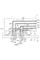
- FIG. 2 shows a structure around the relay unit 3 of the optical modulator 1 in the present embodiment.
- the substrate 41 has four signal electrodes 43A, 43B, 43C, and 43D.
- Each of the signal electrodes 43A, 43B, 43C, and 43D includes a main body 43a extending in parallel with the optical waveguide 42 (see FIG. 1), and a lead-out portion 43b that draws an electrode from the side end 41c of the substrate 41 to the end of the main body 43a. And having.
- Each of the signal electrodes 43A, 43B, 43C, and 43D is configured to bend from an end portion of the main body portion 43a extending in parallel to the side end portion 41c, and the lead portion 43b extends toward the side end portion 41c.
- each signal electrode 43A, 43B, 43C, 43D is arranged in this order from the side opposite to the side end 41c, and the lead-out portion of each signal electrode 43A, 43B, 43C, 43D. 43b is arranged in this order from the end 41a side.
- the number may be less or more than four.
- Connectors 61A, 61B, 61C, 61D for external connection are arranged in parallel in this order from the end 41a side of the substrate 41 on the side wall 11 of the housing 10. In addition, this connector position may have a space
- An external connector 70 for inputting a signal to the optical modulator 1 is attached to the connectors 61A, 61B, 61C, 61D.
- the relay unit 3 includes a relay substrate 51 and relay electrodes 52A, 52B, 52C, and 52D that transmit signals to the signal electrodes 43A, 43B, 43C, and 43D.
- the relay board 51 is divided into relay boards 51A, 51B, 51C, and 51D.
- the divided relay boards 51 ⁇ / b> A, 51 ⁇ / b> B, 51 ⁇ / b> C, 51 ⁇ / b> D are made of a rectangular plate material, and are provided between the side end 41 c of the board 41 and the side wall 11 of the housing 10.
- the relay boards 51A, 51B, 51C, 51D are made of alumina, for example.
- the relay electrodes 52A, 52B, 52C, and 52D are divided and arranged in parallel on the relay boards 51A, 51B, 51C, and 51D in this order from the end 41a side, and the signal electrodes 43A, 43B, and 43C are arranged. , 43D are electrically connected to each other.
- the relay electrodes 52A, 52B, 52C, and 52D extend from the end portion 51a on the substrate 41 side to the end portion 51b on the side wall portion 11 side of the housing 10.
- the relay electrodes 52A, 52B, 52C, and 52D are electrically connected to the lead portions 43b of the signal electrodes 43A, 43B, 43C, and 43D at the end portion 51a on the substrate 41 side, and externally connected at the end portion 51b on the side wall portion 11 side. Are electrically connected to the connectors 61A, 61B, 61C, 61D.
- the connection method in connection part 56A, 56B, 56C, 56D will not be specifically limited if electrical connection is possible, However, You may employ
- the relay electrodes 52A, 52B, 52C, and 52D may extend in an inclined state from the end 51a toward the end 51b, or may extend straight.
- each relay board 51A, 51B, 51C, 51D can be reduced, and the stress on the relay board can be reduced due to temperature changes.
- a filter made of a capacitor or a resistor for adjusting the high frequency characteristics of the optical modulator 1 may be mounted on the relay substrate 51.
- the total length of the signal electrode 43A and the relay electrode 52A, the total length of the signal electrode 43B and the relay electrode 52B, the total length of the signal electrode 43C and the relay electrode 52C, and the signal electrode 43D and the relay is preferably equal to each other.
- the total length means the length from the end portion 51a of the substrate 41 to the start point of the portion (action portion) contributing to the modulation of the optical waveguide 42 for the signal electrodes 43A, 43B, 43C, and 43D, and the relay electrode.
- the total length of 52A, 52B, 52C, and 52D are the total length of 52A, 52B, 52C, and 52D.
- the length adjustment unit is formed by winding the wiring of either the substrate 41 or the relay substrate 51, or by shifting the position of the starting point of the action unit for each branch waveguide constituting each Mach-Zehnder unit 421,422. And the total length may be made equal.
- the length adjustment is performed on the substrate 41 side, but the signal electrodes 43A, 43B, 43C, and 43D are formed straight, and the length adjustment is performed on the relay electrodes 52A, 52B, 52C, and 52D side.
- a part may be provided. Accordingly, the sizes of the relay boards 51A, 51B, 51C, and 51D are also increased. When such a structure is adopted, it is possible to simplify the wiring of the wiring on the substrate 41 side.
- the size of the substrate 41 can be reduced. Further, since the signal electrodes 43A, 43B, 43C, and 43D on the substrate 41 have a narrower signal electrode line and a larger loss than the relay electrodes 52A, 52B, 52C, and 52D, the electrodes are formed on the relay substrate 51. It may be preferable to crawl. In the structure shown in FIG. 2, the wiring of the relay boards 51A, 51B, 51C, and 51D can be simplified and the relay boards 51A, 51B, 51C, and 51D can be downsized.
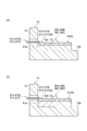
- the relay boards 51A, 51B, 51C and 51D may be installed on an installation surface 12a provided on the housing 10 itself as shown in FIG. According to the configuration illustrated in FIG. 3A, the pedestal portion 12 that protrudes from the bottom surface 10 e of the housing 10 is provided at a position where the relay boards 51 ⁇ / b> A, 51 ⁇ / b> B, 51 ⁇ / b> C, and 51 ⁇ / b> D are disposed. Becomes the installation surface 12a. Note that a conductive adhesive is filled between the installation surface 12a and the installation surfaces 51e of the relay boards 51A, 51B, 51C, and 51D. In this way, the number of parts can be reduced by installing the relay boards 51A, 51B, 51C, 51D in the housing 10 itself.
- the intermediate member 20 is provided on the bottom surface 10e of the housing 10 at the position where the relay boards 51A, 51B, 51C, 51D are arranged, and the upper surface of the intermediate member 20 is It becomes the installation surface 20a.
- the intermediate material 20 is preferably a conductive material such as a metal material in order to firmly establish the GND connection between the relay substrates 51A, 51B, 51C, and 51D and the housing 10.
- the intermediate member 20 uses a material between the linear expansion coefficient of the relay boards 51A, 51B, 51C, 51D and the linear expansion coefficient of the housing 10.
- the material of the relay boards 51A, 51B, 51C and 51D is alumina (6.7 ⁇ 10 ⁇ 6 / K), and the material of the housing 10 is stainless steel (SUS304) (17.3 ⁇ 10 ⁇ 6 / K).
- the material of the intermediate member 20 having a linear expansion coefficient between them is preferably between 8 ⁇ 10 ⁇ 6 / K and 15 ⁇ 10 ⁇ 6 / K, specifically, nickel (13 ⁇ 10 ⁇ 6 / K), cobalt (12 ⁇ 10 ⁇ 6 / K) and alloys thereof (around 10 ⁇ 10 ⁇ 6 / K), stainless steel (SUS403) (10 ⁇ 10 ⁇ 6 / K), and the like.
- a conductive adhesive is filled between the installation surface 20a and the installation surfaces 51e of the relay boards 51A, 51B, 51C, and 51D.
- solder, AuSu brazing material, or the like is also used. These are also filled between the housing 10 and the intermediate member 20.
- the relay boards 51A, 51B, 51C, 51D are installed on the intermediate member 20 having a linear expansion coefficient smaller than that of the casing 10 and larger than that of the relay boards 51A, 51B, 51C, 51D.
- the difference in size change due to the temperature change between the relay boards 51A, 51B, 51C, 51D and the installation surface 20a is reduced. Therefore, the thermal stress generated in the relay boards 51A, 51B, 51C, 51D can be reduced.
- the relay substrate 51 is divided between the relay electrodes 52A, 52B, 52C, and 52D, and the adjacent relay electrodes correspond to the first relay electrode and the second relay electrode, respectively.
- the relay board 51A is provided with the relay electrode 52A, the relay board 51B with the relay electrode 52B, the relay board 51C with the relay electrode 52C, and the relay board 51D with the relay electrode 52D.
- a gap GP is formed between the end portions 51c of the relay boards 51A, 51B, 51C, 51D facing each other.
- each of the relay boards 51A, 51B, 51C, 51D is completely divided, and the end portion 51c related to the divided portion is in the whole area between the end portion 51a on the substrate 41 side and the end portion 51b on the side wall portion 11 side. It is formed over.
- the end portion 51c related to the divided portion has a shape extending straight and perpendicular to the end portions 51a and 51b.
- the shape of the end 51c related to the divided portion is not particularly limited. For example, it may be inclined, may be bent or curved.
- the size of the gap GP between the relay boards 51A, 51B, 51C, 51D is not particularly limited, and the sizes of the gaps GP may be different or the same.
- the lead portions 243b of the plurality of signal electrodes 243A, 243B, 243C, and 243D are provided in a state of being arranged in close proximity to each other. That is, the connecting portions 256A, 256B, 256C, and 256D of the signal electrodes 243A, 243B, 243C, and 243D and the relay electrodes 252A, 252B, 252C, and 252D are arranged in close proximity to each other.
- connection portions 256A, 256B, 256C, and 256D are gathered as much as possible (as shown in FIG. 7 described later). It is preferable that at least a pair of connection portions are gathered even if the connection portions are not gathered).
- FIG. 8A shows the optical waveguide and electrode structure of the DP-QPSK modulator
- FIG. 8B shows the optical waveguide and electrode structure of the QAM modulator.
- the output waveguide 42b is multiplexed with an amplitude ratio of 2: 1, for example.
- the arrangement of the lead-out portions 43b of the signal electrodes 43 is concentrated in one place.
- the total length of each signal electrode and relay electrode needs to be equal in order to eliminate the phase difference between signals. Therefore, it is necessary to provide a length adjusting portion (for example, the length adjusting portion 43c shown in FIG. 2) on the signal electrode.
- a length adjusting portion for example, the length adjusting portion 43c shown in FIG. 2
- the difference in length between one signal electrode 143 and the other signal electrode 143 becomes large, and the wiring in the length adjusting section is ugly. The turn must be very large.
- restrictions are imposed in the design of scooping due to the relationship with the arrangement of other components on the substrate 141.
- the length adjusting unit 143c related to a plurality of reciprocations is formed as shown in FIG. 4B in order to increase the amount of wiring in the length adjusting unit.
- the space between the end portion 141c and the main body portion 143a becomes large, and there arises a problem that the substrate 141 cannot be reduced in size (however, in the present invention, the length adjusting portion as shown in FIG. It does not exclude the light modulators used).
- the effect on the component cost when the substrate size is increased is lower in the relay substrate than in the waveguide substrate. Therefore, it is preferable to provide a length adjusting portion on the relay board in terms of both characteristics and cost.
- connection portions 256A, 256B, 256C, and 256D are combined as much as possible, but FIG.
- the connection portions 256A, 256B, 256C, and 256D are combined as much as possible, but FIG.
- the following problem occurs.
- the size of the relay board 251 increases. Further, in the manufacture of an optical modulator, a high temperature of several hundred degrees Celsius is used when mounting parts of a waveguide substrate or a relay substrate, for example, 200 degrees Celsius when curing a conductive adhesive, 300 degrees Celsius when soldering, and 500 degrees Celsius when joining a brazing material. May be about. As shown in FIG. 4D, the relay board 251 is installed on the housing 10, but the linear expansion coefficient of the material of the relay board 251 is different from the linear expansion coefficient of the material of the housing 10. Therefore, when a temperature change occurs, thermal stress is generated near the boundary portion between the relay substrate 251 and the housing 10 (portion indicated by CE in the drawing), and the relay substrate 251 may be cracked or cracked. This becomes more prominent as the size of the relay substrate 251 increases.
- the relay electrodes 52A, 52B, 52C, and 52D are arranged in parallel on the relay substrate 51, and the relay substrate 51 is connected to each relay substrate 51A, 51B, 51C, It is divided between 51D.
- the relay board 51 by dividing the relay board 51 into a plurality of relay boards 51A, 51B, 51C, 51D, the thermal stress on the relay board 51 can be reduced. As a result, cracks and cracks in the relay substrate 51 can be suppressed.
- optical modulator according to the present invention is not limited to the above embodiment.
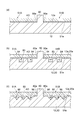
- FIGS. 5A and 6 between the divided relay boards 51A, 51B, 51C, and 51D, there is a housing 10 in which the relay boards 51A, 51B, 51C, and 51D are installed. It may be partitioned off by a convex portion 80 extending from the installation surface 12a of the pedestal portion 12 (or the installation surface 20a of the intermediate member 20 as shown in FIG. 9A). As shown in FIG. 9B, the relay boards 51A, 51B, 51C, and 51D are installed on the intermediate material 20, and the convex portion 80 protrudes from the bottom surface of the housing 10 on which the intermediate material 20 is installed. May be.
- the relay boards 51A, 51B, 51C, 51D may be mounted on the housing 10 after being mounted on the intermediate material 20, or the relay boards 51A, 51B, 51C, 51D may be mounted on the housing 10 after the intermediate material 20 is mounted on the housing 10. It may be mounted on the intermediate material 20.
- 5A is provided for a partial region of the end 51c of the relay boards 51A, 51B, 51C, and 51D, but may be provided for the entire region. . That is, the convex part 80 may extend from the end part 51a to the end part 51b.
- the cross-sectional shape of the convex portion 80 is rectangular, but the shape is not particularly limited, and may be U-shaped, semicircular, triangular, or the like.
- both side surfaces 80a functioning as mating surfaces for the side surfaces of the relay substrates 51A, 51B, 51C, 51D are preferably flat.
- a conductive adhesive AD is filled between the relay boards 51A, 51B, 51C, 51D and the installation surface 12a (or the installation surface 20a). According to the configuration as described above, positioning in the direction along the side end portion 41c can be easily and accurately performed by abutting the divided relay boards 51A, 51B, 51C, and 51D on the convex portions 80, respectively. Can do.
- the optical modulator uses a high frequency signal, the positional relationship and gap between the board and the connector pins affect the high frequency characteristics. Since these alignment tolerances are as small as about 20 ⁇ m, it is important to perform alignment accurately.
- a positioning portion 81 may be provided that faces the side end portion 41c of the substrate 41 with the relay substrates 51A, 51B, 51C, 51D interposed therebetween.
- the positioning portion 81 shown in FIG. 5B is provided for a partial region of the end portion 51b of the relay boards 51A, 51B, 51C, 51D, but may be provided for the entire region. .
- the side wall part 11 itself of the housing 10 may function as the positioning part 81.
- uneven portions 83 and 85 are formed on the installation surface 12a (or the installation surface 20a) on which the relay boards 51A, 51B, 51C and 51D are installed. It's okay.
- the uneven portion 83 shown in FIG. 6B is configured by arranging a plurality of grooves 84 having a rectangular cross section at a predetermined interval.
- the concave-convex portion 85 shown in FIG. 6C is configured by arranging a plurality of grooves 86 having a triangular cross section at a predetermined interval.
- grooved parts 83 and 85 may be provided with respect to the whole area
- the direction in which the grooves 84 and 86 constituting the concavo-convex portions 83 and 85 extend is not particularly limited. As shown in FIG. May extend in a direction perpendicular to the extending direction of the convex portion 80 (a direction parallel to the side end portion 41c of the substrate 41).
- the direction of the unevenness when the difference between the lengths in the longitudinal direction and the short direction is large, it is more preferable to set the direction of the unevenness so that the longitudinal direction has unevenness. It is. According to the configuration as described above, the area where the relay boards 51A, 51B, 51C, 51D are in contact with the installation surface 12a (or the installation surface 20a) can be reduced, so that the relay boards 51A, 51B, 51C, 51D The generated thermal stress can be reduced.
- the uneven portion may be provided on the installation surface 51e of the relay boards 51A, 51B, 51C, 51D instead of the installation surface 12a (or the installation surface 20a), and the installation surface 51e and the installation surface 12a (or installation surface). It may be provided on both of the surfaces 20a).
- the grooves 84 and 86 with a conductive adhesive having a low Young's modulus, stress can be relieved and the GND connection can be made firmly.
- the four relay electrodes 52A, 52B, 52C, and 52D (and the connection portions 56A, 56B, 56C, and 56D) are arranged side by side.
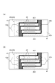
- FIG. 52B (and connection portions 56A and 56B) are arranged in parallel, and a pair of relay electrodes 52C and 52D (and connection portions 56C and 56D) are arranged in parallel, but the relay electrodes 52A and 52B and the relay electrodes 52C and 52D are It may be in a state of being spaced apart from each other and not being juxtaposed. In this state, as shown in FIG.
- the relay board 351 for the relay electrodes 52A and 52B and the relay board 351 for the relay electrodes 52C and 52D are individually provided.
- One relay substrate 351 is divided into a relay substrate 351A and a relay substrate 351B between the relay electrode 52A and the relay electrode 52B.
- the other relay substrate 351 is divided into a relay substrate 351C and a relay substrate 351D between the relay electrode 52C and the relay electrode 52D.
- a groove portion 360 is formed in the pedestal portion 12 (or the intermediate member 20) of the housing 10, and the bottom surface of the groove portion 360 is set as an installation surface. It is good also as 12a (or installation surface 20a).
- each side surface of the groove portion 360 functions as a positioning portion for the relay boards 351A and 351B.
- a convex portion 380 for positioning is formed between the groove portion 360 for the relay substrate 351A and the groove portion 360 for the relay substrate 351B.
- a similar groove 360 structure may be applied to the relay boards 351C and 351D. Further, the groove structure having the same purpose may be applied to the relay boards 51A, 51B, 51C, and 51D shown in FIG.
- the example in which the relay substrate is divided for each relay electrode has been shown so far, but the number of relay electrodes per relay substrate is not limited to one.
- the relay electrodes are combined in one pair and two relay electrodes are formed on one relay substrate, the characteristics of the paired signals can be made uniform as described above.
- DESCRIPTION OF SYMBOLS 1 Optical modulator, 10 ... Housing, 20 ... Intermediate material, 41 ... Substrate, 51, 351 ... Relay substrate, 51A, 51B, 51C, 51D, 351A, 351B, 351C, 351D ... Relay substrate (divided relay Substrate), 52A, 52B, 52C, 52D ... relay electrode, 80 ... convex portion, 83, 85 ... uneven portion.
Landscapes
- Physics & Mathematics (AREA)
- Nonlinear Science (AREA)
- General Physics & Mathematics (AREA)
- Optics & Photonics (AREA)
- Chemical & Material Sciences (AREA)
- Engineering & Computer Science (AREA)
- Ceramic Engineering (AREA)
- Crystallography & Structural Chemistry (AREA)
- Optical Modulation, Optical Deflection, Nonlinear Optics, Optical Demodulation, Optical Logic Elements (AREA)
Abstract
複数本の光導波路及び複数本の信号電極が形成された基板と、外部からの信号を信号電極へ伝達する中継基板と、基板及び前記中継基板を収容する筐体と、を備え、中継基板上には、信号を信号電極へ伝達する第1の中継電極、及び第2の中継電極が設けられ、中継基板は、第1の中継電極と第2の中継電極との間で分割されている、光変調器。
Description
本発明は、光変調器に関する。
従来、光変調器として、複数本の光導波路及び信号電極が形成された基板と、外部からの信号を信号電極へ伝達する中継基板と、基板及び中継基板を収容する筐体と、を備える光変調器が知られている。中継基板上には、信号を信号電極へ伝達する複数の中継電極が形成されている。この光変調器では、筐体に取り付けられたコネクタを介して外部から信号が入力され、基板の信号電極へ中継基板を介して伝達される。
ここで、大容量の光通信に対応する光変調器においては、信号の入力が多くなり、それに伴って中継基板のサイズが大きくなる。ここで、中継基板の材料と筐体の材料とは互いに異なるため、線膨張係数が互いに異なる。従って、温度変化が生じると熱応力が発生し、中継基板に割れやクラックなどが生じる可能性がある。このような問題は、中継基板のサイズが大きくなるほど顕著である。
本発明は、中継基板の割れやクラックを抑制できる光変調器を提供することを目的とする。
本発明の一側面に係る光変調器は、複数本の光導波路及び複数本の信号電極が形成された基板と、外部からの信号を信号電極へ伝達する中継基板と、基板及び中継基板を収容する筐体と、を備え、中継基板上には、信号を信号電極へ伝達する第1の中継電極、及び第2の中継電極が設けられ、中継基板は、第1の中継電極と第2の中継電極との間で分割されている。
この光変調器では、中継基板上に第1の中継電極及び第2の中継電極が設けられており、中継基板が、第1の中継電極と第2の中継電極との間で分割されている。このように、中継基板を複数に分割することにより、中継基板に対する熱応力を低減させることができる。これによって、中継基板の割れやクラックを抑制することができる。
また、本発明の他の側面に係る光変調器では、分割された中継基板同士の間は、当該中継基板が設置される設置面側から延びる凸部で仕切られていてよい。これによれば、分割された中継基板をそれぞれ凸部に突き当てることによって、分割された中継基板の位置決めを容易かつ高精度に行うことができる。
また、本発明の他の側面に係る光変調器では、中継基板が設置される設置面と、設置面上に設置される中継基板の被設置面との少なくとも一方には、凹凸部が形成されていてよい。これによれば、中継基板と設置面とが接する面積を少なくすることができるため、中継基板に発生する熱応力を低減することができる。
また、本発明の他の側面に係る光変調器において、中継基板は、筐体上に設置されていてよい。このように、筐体自体に中継基板を設置することにより、部品点数を低減することができる。
また、本発明の他の側面に係る光変調器において、中継基板は、中間材上に設置され、中間材の線膨張係数は、中継基板の線膨張係数と、筐体の線膨張係数との中間のものとするとよい。これによって、筐体上に中継基板を設置した場合に比して、中継基板と設置面との間の温度変化を小さくすることができるため、中継基板に発生する熱応力を低減することができる。
本発明によれば、中継基板の割れやクラックを抑制できる。
以下、添付図面を参照して本発明の実施形態を詳細に説明する。
図1は、一実施形態に係る光変調器を概略的に示す図である。図1に示されるように、光変調器1は、光ファイバF1によって導入された入力光を変調して、光ファイバF2に変調光を出力する装置である。光変調器1は、光入力部2と、中継部3と、光変調素子4と、終端部5と、光出力部6と、モニタ部7と、筐体10と、を備え得る。
筐体10は、一方向(以下、「方向A」という。)に延びる箱型の部材であって、例えばステンレス鋼から構成されている。筐体10は、方向Aにおける両端面である一端面10a及び他端面10bを有する。一端面10aには光ファイバF1を挿入するための開口が設けられている。他端面10bには光ファイバF2を挿入するための開口が設けられている。筐体10は、例えば、光入力部2、中継部3、光変調素子4、終端部5、光出力部6及びモニタ部7を収容する。
光入力部2は、光ファイバF1によって導入される入力光を光変調素子4に供給する。光入力部2は、光ファイバF1と光変調素子4との接続を補助するための補助部材を備えてもよい。
中継部3は、外部から供給される電気信号である変調信号を中継して光変調素子4に出力する。中継部3は、例えば筐体10の側面10cに設けられた変調信号入力用のコネクタを介して変調信号を入力し、光変調素子4に変調信号を出力する。
光変調素子4は、中継部3から出力される変調信号に応じて、光入力部2から供給される入力光を変調光に変換する装置であって、例えばLN光変調素子である。光変調素子4は、基板41と、光導波路42と、信号電極43と、を備え得る。基板41は、例えばニオブ酸リチウム(LiNbO3、以下「LN」という。)などの電気光学効果を奏する誘電体材料から構成されている。基板41は方向Aに沿って延びており、方向Aにおける両端部である一端部41a及び他端部41bを有する。
光導波路42は、基板41上に設けられている。光導波路42は、例えばマッハツェンダ(Mach-Zehnder)型の光導波路であって、光変調素子4の変調方式に応じた構造を有する。この例では、光変調素子4の変調方式は、QPSK(Quadrature Phase Shift Keying:4値位相変調)方式である。この場合、光導波路42は、マッハツェンダ部420の2つの分岐導波路上に、マッハツェンダ部421及びマッハツェンダ部422が設けられた構造を有する。すなわち、マッハツェンダ部420の入力導波路42aは基板41の一端部41aから方向Aに沿って延び、分岐されてマッハツェンダ部421の入力端及びマッハツェンダ部422の入力端にそれぞれ接続されている。マッハツェンダ部420の出力導波路42bでは、マッハツェンダ部421の出力端及びマッハツェンダ部422の出力端から延びる導波路が合流して方向Aに沿って他端部41bまで延びている。
信号電極43は、変調信号に応じた電界を光導波路42に印加するための部材であって、基板41上に設けられている。信号電極43の配置及び数は、基板41の結晶軸の向き及び光変調素子4の変調方式に応じて決定される。各信号電極43には、中継部3から出力される変調信号がそれぞれ印加される。
光変調素子4では、光入力部2から光変調素子4に入力される入力光は、入力導波路42aによってマッハツェンダ部421及びマッハツェンダ部422に分岐して入力される。入力光は、マッハツェンダ部421及びマッハツェンダ部422においてそれぞれ変調される。マッハツェンダ部421において変調された変調光及びマッハツェンダ部422において変調された変調光は、出力導波路42bにおいて合波されて光変調素子4から出力される。
終端部5は、変調信号の電気的終端である。終端部5は、光変調素子4の信号電極43の各々に対応した抵抗器を備え得る。各抵抗器の一端は光変調素子4の信号電極43に電気的に接続され、各抵抗器の他端は接地電位に接続されている。各抵抗器の抵抗値は、信号電極43の特性インピーダンスと略等しく、例えば50Ω程度である。
光出力部6は、光変調素子4から出力される変調光を光ファイバF2に出力する。光出力部6は、基板41の他端部41bに設けられている。
モニタ部7は、例えば、各マッハツェンダ部421,422の光出力の相補的な光強度をモニタする。モニタ部7は光電変換素子を備え得る。光電変換素子は、光信号を電気信号に変換するための素子であって、例えばフォトダイオードである。光電変換素子は、例えば基板41上で、マッハツェンダ部420の出力導波路42bと分岐した導波路上に置かれ、導波路から漏れだしたエバネッセント波を受光し、その光強度に応じた電気信号をバイアス制御部(不図示)に出力する。なお、モニタ部7は、光変調素子4から出力される放射光の光強度をモニタしてもよい。
図2に、本実施形態における光変調器1の中継部3周辺の構造を示す。図2に示すように、基板41は、四本の信号電極43A,43B,43C,43Dを有している。各信号電極43A,43B,43C,43Dは、光導波路42(図1参照)と平行に延びる本体部43aと、基板41の側端部41cから本体部43aの端部まで電極を引き出す引出部43bと、を有する。各信号電極43A,43B,43C,43Dは、側端部41cに平行に延びる本体部43aの端部から屈曲して、側端部41cに向かって引出部43bが延びる構成となっている。本実施形態では、各信号電極43A,43B,43C,43Dの本体部43aが側端部41cの反対側からこの順で並設されており、各信号電極43A,43B,43C,43Dの引出部43bが端部41a側からこの順で並設されている。なお、本実施形態では、信号電極43A,43B,43C,43Dが四本設けられている例について説明しているが、四本より少なくてもよく、多くてもよい。
筐体10の側壁部11には、外部接続のためのコネクタ61A,61B,61C,61Dが、基板41の端部41a側からこの順で並設されている。なお、このコネクタ位置は、規格化により、間隔や配置が定められている場合もある。当該コネクタ61A,61B,61C,61Dには、光変調器1に信号を入力する外部コネクタ70が取り付けられる。
中継部3は、中継基板51と、信号を信号電極43A,43B,43C,43Dへ伝達する中継電極52A,52B,52C,52Dと、を備えている。中継基板51は、中継基板51A,51B,51C,51Dに分割されている。分割された中継基板51A,51B,51C,51Dは、矩形状の板材によって構成され、基板41の側端部41cと、筐体10の側壁部11との間に設けられている。中継基板51A,51B,51C,51Dは、例えばアルミナなどによって構成される。中継電極52A,52B,52C,52Dは、中継基板51A,51B,51C,51D上において、端部41a側からこの順で各中継基板に分かれて並設されており、信号電極43A,43B,43C,43Dとそれぞれ電気的に接続されている。中継電極52A,52B,52C,52Dは、基板41側の端部51aから筐体10の側壁部11側の端部51bまで延びている。中継電極52A,52B,52C,52Dは、基板41側の端部51aにおいて信号電極43A,43B,43C,43Dの引出部43bと電気的に接続され、側壁部11側の端部51bにおいて外部接続のためのコネクタ61A,61B,61C,61Dと電気的に接続されている。なお、接続部56A,56B,56C,56Dでの接続方法は、電気的な接続が可能であれば特に限定されないが、図3に示すようにワイヤボンディングを採用してもよい。中継電極52A,52B,52C,52Dは、端部51aから端部51bへ向かって、傾斜した状態で延びていてもよく、真っ直ぐに延びていてもよい。このように、中継基板51を複数に分けることにより、個々の中継基板51A,51B,51C,51Dのサイズが小さくなり、温度変化により中継基板に係る応力を小さくすることができる。また、中継基板51上には光変調器1の高周波特性を調整するためのコンデンサや抵抗からなるフィルタを実装してもよい。
信号の位相差を無くすため、信号電極43A及び中継電極52Aの合計長さ、信号電極43B及び中継電極52Bの合計長さ、信号電極43C及び中継電極52Cの合計長さ、並びに信号電極43D及び中継電極52Dの合計長さは、互いに等しいことが好ましい。ただし、ここで合計長さとは、信号電極43A,43B,43C,43Dについての、基板41の端部51aから光導波路42の変調に寄与する部分(作用部)の始点までの長さと、中継電極52A,52B,52C,52Dの長さの合計とする。そのためには、基板41もしくは中継基板51の何れかの配線を這い回したり、作用部の始点の位置を各マッハツェンダ部421,422を構成する各分岐導波路毎にずらしたりして長さ調整部を設け、合計長さを等しくすればよい。また、図2の例では、基板41側で長さ調整を行っているが、信号電極43A,43B,43C,43Dは真っ直ぐに形成し、中継電極52A,52B,52C,52D側に長さ調整部を設けてもよい。それに伴って、中継基板51A,51B,51C,51Dのサイズも大きくなる。このような構造を採用した場合、基板41側での配線の這い回しをシンプルにすることができる。従って、基板41のサイズを小さくすることができる。また、基板41上の信号電極43A,43B,43C,43Dの方が信号電極線が細く中継電極52A,52B,52C,52Dよりもロスの大きな構造であるために、中継基板51上にて電極を這い回した方が好ましい場合がある。なお、図2に示す構造では、中継基板51A,51B,51C,51D側の配線の這い回しをシンプルにすることができると共に、当該中継基板51A,51B,51C,51Dを小型にできる。
中継基板51A,51B,51C,51Dは、図3(a)に示すように筐体10自体に設けられた設置面12a上に設置されてよい。図3(a)に示す構成によれば、中継基板51A,51B,51C,51Dが配置される位置に、筐体10の底面10eから突出する台座部12が設けられ、当該台座部12の上面が設置面12aとなる。なお、設置面12aと、中継基板51A,51B,51C,51Dの被設置面51eとの間には、導電性接着剤が充填される。このように、筐体10自体に中継基板51A,51B,51C,51Dを設置することにより、部品点数を低減することができる。
あるいは、図3(b)に示すように筐体10上に配置されている中間材20の設置面20a上に設置されてもよい。図3(b)に示す構成によれば、中継基板51A,51B,51C,51Dが配置される位置において、筐体10の底面10e上に中間材20が設けられ、当該中間材20の上面が設置面20aとなる。なお、中間材20は中継基板51A,51B,51C,51Dと筺体10のGND接続を強固に行うために金属材料等の導電性材料が望ましい。中間材20は中継基板51A,51B,51C,51Dの線膨張係数と筺体10の線膨張係数の間のものを用いる。中継基板51A,51B,51C,51Dの材料がアルミナ(6.7×10-6/K)であり、筐体10の材料がステンレス(SUS304)(17.3×10-6/K)であった場合、その間の線膨張係数を有する中間材20の材料としては8×10-6/K~15×10-6/Kの間が望ましく、具体的には、ニッケル(13×10-6/K)、コバルト(12×10-6/K)及びそれらの合金(10×10-6/K前後)、ステンレス(SUS403)(10×10-6/K)などがある。なお、設置面20aと、中継基板51A,51B,51C,51Dの被設置面51eとの間には、導電性接着剤が充填される。また、導電性接着剤の他にも、ハンダやAuSuのろう材なども用いられる。なお、これらは筐体10と中間材20との間にも充填されている。このように、中継基板51A,51B,51C,51Dが、筐体10よりも小さく中継基板51A,51B,51C,51Dよりも大きい線膨張係数を有する中間材20上に設置されることによって、筐体10上に中継基板51A,51B,51C,51Dを設置した場合に比して、中継基板51A,51B,51C,51Dと設置面20aとの間の温度変化によるサイズ変化の差を小さくすることができるため、中継基板51A,51B,51C,51Dに発生する熱応力を低減することができる。
ここで、中継基板51は、各中継電極52A,52B,52C,52Dの間で分割されており、それぞれ隣り合う中継電極が第1の中継電極、第2の中継電極に相当する。すなわち、分割された中継基板51Aには中継電極52A、中継基板51Bには中継電極52B、中継基板51Cには中継電極52C、中継基板51Dには中継電極52Dが設けられている。各中継基板51A,51B,51C,51Dの互いに対向する端部51c同士の間には、隙間GPが形成される。各中継基板51A,51B,51C,51Dは、完全に分割されており、分割部分に係る端部51cは、基板41側の端部51aと側壁部11側の端部51bとの間の全域に亘って形成されている。なお、図2に示す例では、分割部分に係る端部51cは、端部51a,51bと垂直に真っ直ぐに延びる形状であるが、中継基板51A,51B,51C,51Dが分割されている限り、分割部分に係る端部51cの形状は特に限定されない。例えば、傾斜していてもよく、屈曲していても湾曲していてもよい。また、各中継基板51A,51B,51C,51D同士の間の隙間GPの大きさは特に限定されず、各隙間GPの大きさが互いに異なっていても同じであってもよい。
次に、本実施形態に係る光変調器1の作用・効果について説明する。
まず、図4を参照して、光変調器の前提構成、及び従来の光変調器の構成について説明する。光変調器の分野においては、図4(c)に示すように、複数の信号電極243A,243B,243C,243Dの引出部243bは、互いに近接して並設された状態で設けられる。すなわち、信号電極243A,243B,243C,243Dと中継電極252A,252B,252C,252Dとの接続部256A,256B,256C,256Dは、互いに近接して並設されている。従って、基板241の側端部241cが長く広い範囲を有しているとしても、接続部256A,256B,256C,256Dは極力一箇所にまとめられることが好ましい(後述の図7のように、全ての接続部がまとめられていなくとも、少なくとも一対の接続部がまとめられていることが好ましい)。
また、光変調器の分野においては、図1に示したQPSK変調方式の他にもDP-QPSK変調(Dual Polarization-Quadrature Phase Shift Keying:偏波直交4値位相変調)方式やQAM変調(Quadrature Amplitude Modulation:直角位相振幅変調)などがある。図8(a)にDP-QPSK変調器の光導波路及び電極構造を、図8(b)にQAM変調器の光導波路及び電極構造を示す。QAM変調器では、出力導波路42bにおいて、例えば2:1の振幅比で合波する。このような光導波路の構造により、信号電極43の引出部43bの配置は一か所にまとめて密集することになる。少なくとも変調部毎に一対にまとまっていることにより、基板間の距離やボンディング長、中継基板とピンの位置などの実装による特性の影響を揃えることができ、周波数応答特性のバランスや、電極間の電気長の整合性に優れた変調器構成とすることができる。
上述のような構成が前提となる理由は以下の通りである。すなわち、図4(a)に示すように、各信号電極143の引出部143b及び接続部156の距離が大きく離れており互いに並設されていない場合、各信号電極143に対して個別の中継基板151が設けられ、それぞれ離れた位置に設置される。この場合、導波路基板と筐体との位置関係のズレが大きくなるなど、位置合わせ精度にも問題が生じる。一方、図4(c)のように各接続部256A、256B,256C,256Dが所定の範囲内で並設されている場合、各中継電極252A,252B,252C,252Dを一の中継基板251でまとめることが可能となり(また、中継基板251内で各中継電極252A,252B,252C,252D同士の間の精度を確保しておくことができる)、位置合わせ工程が容易となり、精度も確保することができる。
また、光変調器の分野においては、信号の位相差を無くすため、それぞれの信号電極及び中継電極の合計長さを等しくする必要がある。従って、信号電極に長さ調整部(例えば、図2に示す長さ調整部43c)を設ける必要がある。しかしながら、図4(a)に示すような構成を採用した場合、一の信号電極143と、他の信号電極143との間で長さの差が大きくなり、長さ調整部での配線の這い回しを非常に大きくしなくてはならなくなる。しかしながら、基板141のうち長さ調整部を設けることができるスペースには限りがある。また、基板141上の他の構成要素の配置との関係から、這い回しの設計において制約を受ける場合がある。また、長さ調整部中の配線間の間隔を狭くし過ぎた場合はクロストークなどの問題が生じる点においても、設計上の制約を受ける。上述のような制約を考慮して、例えば、長さ調整部での配線の這い回しを大きくするために図4(b)に示すように、複数往復に係る長さ調整部143cを形成した場合、端部141cと本体部143aとの間のスペースが大きくなり、基板141を小型化することができないという問題が生じる(ただし、本発明は、図4(b)のような長さ調整部を採用した光変調器を排除するものではない)。また、基板サイズが大きくなった場合の部品コストに対する影響は、導波路基板よりも、中継基板の方が低い。従って、特性面においてもコスト面においても、中継基板に長さ調整部を設けたほうが好ましい。
以上より、光変調器の分野においては、図4(c)に示すように、各接続部256A,256B,256C,256Dが極力一箇所にまとめられる構成が前提となるが、図4(c)に示すように一枚の中継基板251に複数の中継電極252A,252B,252C,252Dを設けた場合、次のような問題が生じる。
すなわち、近年の大容量の光通信の要求に対応するため、信号の入力を多くした場合、中継基板251のサイズが大きくなる。また、光変調器の製造においては、導波路基板や中継基板の部品実装時に数百℃の高温、例えば、導電性接着剤の硬化時には200℃、ハンダ付け時には300℃、ろう材接合時には500℃程度になることがある。図4(d)に示すように、中継基板251は、筐体10上に設置されているが、中継基板251の材料の線膨張係数と、筐体10の材料の線膨張係数は異なる。従って、温度変化が生じると、中継基板251と筐体10との境界部付近(図においてCEで示す部分)において熱応力が発生し、中継基板251に割れやクラック等が生じる可能性がある。これは、中継基板251のサイズが大きくなるほど顕著になる。
これに対し、本実施形態に係る光変調器1では、中継基板51上に中継電極52A,52B,52C,52Dが並設されており、中継基板51が、各中継基板51A,51B,51C,51Dの間で分割されている。このように、中継基板51を複数の中継基板51A,51B,51C,51Dに分割することにより、中継基板51に対する熱応力を低減させることができる。これによって、中継基板51の割れやクラックを抑制することができる。
なお、本発明に係る光変調器は上記実施形態に限定されない。
例えば、図5(a)及び図6に示すように、分割された中継基板51A,51B,51C,51D同士の間は、当該中継基板51A,51B,51C,51Dが設置される筐体10の台座部12の設置面12a(または図9(a)に示すように、中間材20の設置面20a)側から延びる凸部80で仕切られていてよい。なお、図9(b)に示すように、中継基板51A,51B,51C,51Dが中間材20に設置されて、当該中間材20が設置される筐体10の底面から凸部80が突出していてもよい。中継基板51A,51B,51C,51Dは中間材20に実装した後に、筐体10に実装してもよいし、中間材20を筐体10に実装した後に中継基板51A,51B,51C,51Dを中間材20に実装してもよい。図5(a)に示す凸部80は、中継基板51A,51B,51C,51Dの端部51cの一部の領域に対して設けられているが、全領域に対して設けられていてもよい。すなわち、凸部80が、端部51aから端部51bに至るまで延びていてよい。また、図6に示す例では、凸部80の断面形状は矩形であるが、特に形状は限定されず、U字状、半円状、三角形状などであってもよい。ただし、中継基板51A,51B,51C,51Dの側面に対する合わせ面として機能する両側面80aは、平面状であることが好ましい。なお、中継基板51A,51B,51C,51Dと設置面12a(または設置面20a)との間には導電性接着剤ADが充填されている。以上のような構成によれば、分割された中継基板51A,51B,51C,51Dをそれぞれ凸部80に突き当てることによって、側端部41cに沿った方向における位置決めを容易にかつ精度良く行うことができる。
光変調器は、使用する信号の周波数が高いため、基板とコネクタのピンとの位置関係や隙間が高周波特性に影響する。これらの位置合わせのトレランスは20μm程度と小さいために、精度よく位置合わせを行うことが重要である。
また、図5(b)に示すように、基板41の側端部41cに対して中継基板51A,51B,51C,51Dを挟んで対向する位置決め部81を設けてもよい。図5(b)に示す位置決め部81は、中継基板51A,51B,51C,51Dの端部51bの一部の領域に対して設けられているが、全領域に対して設けられていてもよい。中継基板51A,51B,51C,51Dの端部51bを位置決め部81に突き当てることによって、側端部41cと直交する方向における位置決めを容易に行うことができる。なお、図2に示す実施形態においては、筐体10の側壁部11自体を位置決め部81として機能させてもよい。
また、図6(b),(c)に示すように、中継基板51A,51B,51C,51Dが設置される設置面12a(または設置面20a)には、凹凸部83,85が形成されていてよい。図6(b)に示す凹凸部83は、断面矩形状の溝84を所定間隔で複数並設することによって構成されている。図6(c)に示す凹凸部85は、断面三角形状の溝86を所定間隔で複数並設することによって構成されている。なお、凹凸部83,85は、中継基板51A,51B,51C,51Dの被設置面51eの全領域に対して設けられていてよいが、一部の領域に設けられていてもよい。また、凹凸部83,85を構成する溝84,86が延びる方向は特に限定されず、図6に示すように凸部80の延在方向に平行な方向(基板41の側端部41cと直交する方向)に延びてもよく、凸部80の延在方向と直交する方向(基板41の側端部41cと平行な方向)に延びてもよい。ただし、中継基板51A,51B,51C,51Dの形状において、長手方向と短手方向の長さの差が大きい場合は、長手方向に凹凸が存在するように凹凸の方向を設定するのがより好適である。以上のような構成によれば、中継基板51A,51B,51C,51Dと設置面12a(または設置面20a)とが接する面積を少なくすることができるため、中継基板51A,51B,51C,51Dに発生する熱応力を低減することができる。なお、凹凸部は、設置面12a(または設置面20a)に代えて中継基板51A,51B,51C,51Dの被設置面51eに設けられてもよく、被設置面51e及び設置面12a(または設置面20a)の両方に設けられてもよい。また、溝84,86に低ヤング率の導電性接着剤を充填することで、応力緩和が可能であり、GND接続を強固に行うことができる。
上述の実施形態では、4つの中継電極52A,52B,52C,52D(及び接続部56A,56B,56C,56D)が並設されていたが、図7に示すように、一対の中継電極52A,52B(及び接続部56A,56B)が並設され、一対の中継電極52C,52D(及び接続部56C,56D)が並設されるが、中継電極52A,52Bと中継電極52C,52Dとは、互いに離間しており並設されていない状態であってもよい。この状態においては、図7(a)に示すように、中継電極52A,52Bに対する中継基板351と中継電極52C,52Dに対する中継基板351は、それぞれ個別に設けられている。また、一方の中継基板351は、中継電極52Aと中継電極52Bとの間で中継基板351A及び中継基板351Bに分割されている。他方の中継基板351は、中継電極52Cと中継電極52Dとの間で中継基板351C及び中継基板351Dに分割されている。
また、図7(b)に示すように、中継基板351A,351Bの設置構造として、筐体10の台座部12(または中間材20)に溝部360を形成し、当該溝部360の底面を設置面12a(または設置面20a)としてもよい。この場合、溝部360の各側面が中継基板351A,351Bの位置決め部として機能する。中継基板351A用の溝部360と中継基板351B用の溝部360との間には位置決め用の凸部380が形成される。なお、中継基板351C,351Dに対しても同様な溝部360の構造を適用してよい。また、図2に示す中継基板51A,51B,51C,51Dに対しても同様な趣旨の溝部の構造を適用してよい。
また、これまでは、各中継電極毎に中継基板を分割する例を示したが、中継基板1枚あたりの中継電極数は、1本に限らない。特に、中継電極を1対でまとめて、2本の中継電極を1枚の中継基板上に形成すれば、前述のように、対となる信号の特性を揃えることができ好適である。
1…光変調器、10…筐体、20…中間材、41…基板、51,351…中継基板、51A,51B,51C,51D,351A,351B,351C,351D…中継基板(分割された中継基板)、52A,52B,52C,52D…中継電極、80…凸部、83,85…凹凸部。
Claims (5)
- 複数本の光導波路及び複数本の信号電極が形成された基板と、
外部からの信号を前記信号電極へ伝達する中継基板と、
前記基板及び前記中継基板を収容する筐体と、を備え、
前記中継基板上には、信号を前記信号電極へ伝達する第1の中継電極、及び第2の中継電極が設けられ、
前記中継基板は、前記第1の中継電極と前記第2の中継電極との間で分割されている、光変調器。 - 分割された前記中継基板同士の間は、当該中継基板が設置される設置面側から延びる凸部で仕切られている、請求項1に記載の光変調器。
- 前記中継基板が設置される設置面と、前記設置面上に設置される前記中継基板の被設置面との少なくとも一方には、凹凸部が形成されている、請求項1又は2に記載の光変調器。
- 前記中継基板は、前記筐体上に設置されている、請求項1~3の何れか一項に記載の光変調器。
- 前記中継基板は、中間材上に設置され、前記中間材の線膨張係数は、前記中継基板の線膨張係数より大きく、前記筐体の線膨張係数より小さい、請求項1~3の何れか一項に記載の光変調器。
Applications Claiming Priority (2)
| Application Number | Priority Date | Filing Date | Title |
|---|---|---|---|
| JP2013-017714 | 2013-01-31 | ||
| JP2013017714A JP5811111B2 (ja) | 2013-01-31 | 2013-01-31 | 光変調器 |
Publications (1)
| Publication Number | Publication Date |
|---|---|
| WO2014119744A1 true WO2014119744A1 (ja) | 2014-08-07 |
Family
ID=51262441
Family Applications (1)
| Application Number | Title | Priority Date | Filing Date |
|---|---|---|---|
| PCT/JP2014/052313 Ceased WO2014119744A1 (ja) | 2013-01-31 | 2014-01-31 | 光変調器 |
Country Status (2)
| Country | Link |
|---|---|
| JP (1) | JP5811111B2 (ja) |
| WO (1) | WO2014119744A1 (ja) |
Cited By (2)
| Publication number | Priority date | Publication date | Assignee | Title |
|---|---|---|---|---|
| US9740077B2 (en) * | 2015-10-23 | 2017-08-22 | Fujitsu Optical Components Limited | Optical modulator module that includes a plurality of optical modulators |
| US9778539B2 (en) | 2013-03-29 | 2017-10-03 | Sumitomo Osaka Cement Co., Ltd. | Optical modulation device |
Families Citing this family (3)
| Publication number | Priority date | Publication date | Assignee | Title |
|---|---|---|---|---|
| JP6609965B2 (ja) * | 2015-03-31 | 2019-11-27 | 住友大阪セメント株式会社 | 光変調器モジュール |
| JP7013880B2 (ja) * | 2018-01-12 | 2022-02-01 | 住友大阪セメント株式会社 | 光変調器、及び光送信装置 |
| JP7172793B2 (ja) * | 2019-03-27 | 2022-11-16 | 住友大阪セメント株式会社 | 光変調器及びそれを用いた光送信装置 |
Citations (7)
| Publication number | Priority date | Publication date | Assignee | Title |
|---|---|---|---|---|
| JPS59159110A (ja) * | 1983-02-28 | 1984-09-08 | Sumitomo Electric Ind Ltd | 光学部品の接着構造 |
| JPH04163420A (ja) * | 1990-10-26 | 1992-06-09 | Fujitsu Ltd | 光変調器の実装方法 |
| JPH06130338A (ja) * | 1992-10-22 | 1994-05-13 | Fujitsu Ltd | 光導波路デバイス |
| JP2002107594A (ja) * | 2000-09-29 | 2002-04-10 | Ngk Insulators Ltd | 光学部品の接着構造 |
| JP2008276145A (ja) * | 2007-04-05 | 2008-11-13 | Anritsu Corp | 光変調器 |
| JP2011013646A (ja) * | 2009-07-06 | 2011-01-20 | Anritsu Corp | 光変調器モジュールおよびその製造方法 |
| JP2011232583A (ja) * | 2010-04-28 | 2011-11-17 | Anritsu Corp | 光変調器モジュール |
Family Cites Families (3)
| Publication number | Priority date | Publication date | Assignee | Title |
|---|---|---|---|---|
| JP3279210B2 (ja) * | 1997-01-29 | 2002-04-30 | ティーディーケイ株式会社 | 光変調器 |
| JP5326624B2 (ja) * | 2009-02-10 | 2013-10-30 | 富士通オプティカルコンポーネンツ株式会社 | 光変調器 |
| JP5416658B2 (ja) * | 2010-06-07 | 2014-02-12 | アンリツ株式会社 | 光変調器および光変調器モジュール |
-
2013
- 2013-01-31 JP JP2013017714A patent/JP5811111B2/ja active Active
-
2014
- 2014-01-31 WO PCT/JP2014/052313 patent/WO2014119744A1/ja not_active Ceased
Patent Citations (7)
| Publication number | Priority date | Publication date | Assignee | Title |
|---|---|---|---|---|
| JPS59159110A (ja) * | 1983-02-28 | 1984-09-08 | Sumitomo Electric Ind Ltd | 光学部品の接着構造 |
| JPH04163420A (ja) * | 1990-10-26 | 1992-06-09 | Fujitsu Ltd | 光変調器の実装方法 |
| JPH06130338A (ja) * | 1992-10-22 | 1994-05-13 | Fujitsu Ltd | 光導波路デバイス |
| JP2002107594A (ja) * | 2000-09-29 | 2002-04-10 | Ngk Insulators Ltd | 光学部品の接着構造 |
| JP2008276145A (ja) * | 2007-04-05 | 2008-11-13 | Anritsu Corp | 光変調器 |
| JP2011013646A (ja) * | 2009-07-06 | 2011-01-20 | Anritsu Corp | 光変調器モジュールおよびその製造方法 |
| JP2011232583A (ja) * | 2010-04-28 | 2011-11-17 | Anritsu Corp | 光変調器モジュール |
Cited By (2)
| Publication number | Priority date | Publication date | Assignee | Title |
|---|---|---|---|---|
| US9778539B2 (en) | 2013-03-29 | 2017-10-03 | Sumitomo Osaka Cement Co., Ltd. | Optical modulation device |
| US9740077B2 (en) * | 2015-10-23 | 2017-08-22 | Fujitsu Optical Components Limited | Optical modulator module that includes a plurality of optical modulators |
Also Published As
| Publication number | Publication date |
|---|---|
| JP5811111B2 (ja) | 2015-11-11 |
| JP2014149394A (ja) | 2014-08-21 |
Similar Documents
| Publication | Publication Date | Title |
|---|---|---|
| USRE46932E1 (en) | Optical modulator module | |
| JP7283180B2 (ja) | 光変調器 | |
| JP5811111B2 (ja) | 光変調器 | |
| JP5361817B2 (ja) | 光モジュール | |
| JP6136473B2 (ja) | 光変調装置 | |
| JP6458603B2 (ja) | 光デバイス | |
| JP6540744B2 (ja) | 光デバイス | |
| JP6432582B2 (ja) | 光変調器、及び光送信装置 | |
| JP2014199302A (ja) | 光デバイス | |
| CN106997108A (zh) | 光模块 | |
| JP2016020927A (ja) | 光モジュール及び送信装置 | |
| JP2011013646A (ja) | 光変調器モジュールおよびその製造方法 | |
| CN211206992U (zh) | 光调制器及使用了该光调制器的光发送装置 | |
| US11397364B2 (en) | Optical modulator and optical transmission apparatus | |
| US12306479B2 (en) | Optical modulator and optical transmission apparatus using same | |
| US12147097B2 (en) | Optical modulator and optical transmission apparatus using same | |
| US11953767B2 (en) | Optical modulator and optical transmission apparatus using same | |
| JP2002296552A (ja) | 電界吸収型光変調器 |
Legal Events
| Date | Code | Title | Description |
|---|---|---|---|
| 121 | Ep: the epo has been informed by wipo that ep was designated in this application |
Ref document number: 14746908 Country of ref document: EP Kind code of ref document: A1 |
|
| NENP | Non-entry into the national phase |
Ref country code: DE |
|
| 122 | Ep: pct application non-entry in european phase |
Ref document number: 14746908 Country of ref document: EP Kind code of ref document: A1 |