WO2014119103A1 - 光センサ - Google Patents
光センサ Download PDFInfo
- Publication number
- WO2014119103A1 WO2014119103A1 PCT/JP2013/081523 JP2013081523W WO2014119103A1 WO 2014119103 A1 WO2014119103 A1 WO 2014119103A1 JP 2013081523 W JP2013081523 W JP 2013081523W WO 2014119103 A1 WO2014119103 A1 WO 2014119103A1
- Authority
- WO
- WIPO (PCT)
- Prior art keywords
- light
- period
- optical sensor
- light receiving
- emitting element
- Prior art date
- Legal status (The legal status is an assumption and is not a legal conclusion. Google has not performed a legal analysis and makes no representation as to the accuracy of the status listed.)
- Ceased
Links
Images






Classifications
-
- G—PHYSICS
- G01—MEASURING; TESTING
- G01S—RADIO DIRECTION-FINDING; RADIO NAVIGATION; DETERMINING DISTANCE OR VELOCITY BY USE OF RADIO WAVES; LOCATING OR PRESENCE-DETECTING BY USE OF THE REFLECTION OR RERADIATION OF RADIO WAVES; ANALOGOUS ARRANGEMENTS USING OTHER WAVES
- G01S17/00—Systems using the reflection or reradiation of electromagnetic waves other than radio waves, e.g. lidar systems
- G01S17/02—Systems using the reflection of electromagnetic waves other than radio waves
- G01S17/50—Systems of measurement based on relative movement of target
-
- G—PHYSICS
- G01—MEASURING; TESTING
- G01J—MEASUREMENT OF INTENSITY, VELOCITY, SPECTRAL CONTENT, POLARISATION, PHASE OR PULSE CHARACTERISTICS OF INFRARED, VISIBLE OR ULTRAVIOLET LIGHT; COLORIMETRY; RADIATION PYROMETRY
- G01J1/00—Photometry, e.g. photographic exposure meter
- G01J1/02—Details
- G01J1/0204—Compact construction
- G01J1/0209—Monolithic
-
- G—PHYSICS
- G01—MEASURING; TESTING
- G01J—MEASUREMENT OF INTENSITY, VELOCITY, SPECTRAL CONTENT, POLARISATION, PHASE OR PULSE CHARACTERISTICS OF INFRARED, VISIBLE OR ULTRAVIOLET LIGHT; COLORIMETRY; RADIATION PYROMETRY
- G01J1/00—Photometry, e.g. photographic exposure meter
- G01J1/02—Details
- G01J1/0214—Constructional arrangements for removing stray light
-
- G—PHYSICS
- G01—MEASURING; TESTING
- G01J—MEASUREMENT OF INTENSITY, VELOCITY, SPECTRAL CONTENT, POLARISATION, PHASE OR PULSE CHARACTERISTICS OF INFRARED, VISIBLE OR ULTRAVIOLET LIGHT; COLORIMETRY; RADIATION PYROMETRY
- G01J1/00—Photometry, e.g. photographic exposure meter
- G01J1/02—Details
- G01J1/04—Optical or mechanical part supplementary adjustable parts
- G01J1/0407—Optical elements not provided otherwise, e.g. manifolds, windows, holograms, gratings
- G01J1/0411—Optical elements not provided otherwise, e.g. manifolds, windows, holograms, gratings using focussing or collimating elements, i.e. lenses or mirrors; Aberration correction
-
- G—PHYSICS
- G01—MEASURING; TESTING
- G01J—MEASUREMENT OF INTENSITY, VELOCITY, SPECTRAL CONTENT, POLARISATION, PHASE OR PULSE CHARACTERISTICS OF INFRARED, VISIBLE OR ULTRAVIOLET LIGHT; COLORIMETRY; RADIATION PYROMETRY
- G01J1/00—Photometry, e.g. photographic exposure meter
- G01J1/02—Details
- G01J1/04—Optical or mechanical part supplementary adjustable parts
- G01J1/06—Restricting the angle of incident light
-
- G—PHYSICS
- G01—MEASURING; TESTING
- G01J—MEASUREMENT OF INTENSITY, VELOCITY, SPECTRAL CONTENT, POLARISATION, PHASE OR PULSE CHARACTERISTICS OF INFRARED, VISIBLE OR ULTRAVIOLET LIGHT; COLORIMETRY; RADIATION PYROMETRY
- G01J1/00—Photometry, e.g. photographic exposure meter
- G01J1/10—Photometry, e.g. photographic exposure meter by comparison with reference light or electric value provisionally void
- G01J1/16—Photometry, e.g. photographic exposure meter by comparison with reference light or electric value provisionally void using electric radiation detectors
- G01J1/1626—Arrangements with two photodetectors, the signals of which are compared
-
- G—PHYSICS
- G01—MEASURING; TESTING
- G01P—MEASURING LINEAR OR ANGULAR SPEED, ACCELERATION, DECELERATION, OR SHOCK; INDICATING PRESENCE, ABSENCE, OR DIRECTION, OF MOVEMENT
- G01P13/00—Indicating or recording presence, absence, or direction, of movement
-
- G—PHYSICS
- G01—MEASURING; TESTING
- G01S—RADIO DIRECTION-FINDING; RADIO NAVIGATION; DETERMINING DISTANCE OR VELOCITY BY USE OF RADIO WAVES; LOCATING OR PRESENCE-DETECTING BY USE OF THE REFLECTION OR RERADIATION OF RADIO WAVES; ANALOGOUS ARRANGEMENTS USING OTHER WAVES
- G01S7/00—Details of systems according to groups G01S13/00, G01S15/00, G01S17/00
- G01S7/48—Details of systems according to groups G01S13/00, G01S15/00, G01S17/00 of systems according to group G01S17/00
- G01S7/481—Constructional features, e.g. arrangements of optical elements
-
- G—PHYSICS
- G01—MEASURING; TESTING
- G01S—RADIO DIRECTION-FINDING; RADIO NAVIGATION; DETERMINING DISTANCE OR VELOCITY BY USE OF RADIO WAVES; LOCATING OR PRESENCE-DETECTING BY USE OF THE REFLECTION OR RERADIATION OF RADIO WAVES; ANALOGOUS ARRANGEMENTS USING OTHER WAVES
- G01S7/00—Details of systems according to groups G01S13/00, G01S15/00, G01S17/00
- G01S7/48—Details of systems according to groups G01S13/00, G01S15/00, G01S17/00 of systems according to group G01S17/00
- G01S7/481—Constructional features, e.g. arrangements of optical elements
- G01S7/4811—Constructional features, e.g. arrangements of optical elements common to transmitter and receiver
- G01S7/4813—Housing arrangements
Definitions
- the present invention relates to an optical sensor suitably used as a proximity sensor or a gesture sensor, an electronic device using the optical sensor, and the like.
- the optical sensor In liquid crystal panels used for electronic devices such as mobile phones and digital cameras, users operate the electronic devices when their faces are close to the liquid crystal panel in order to reduce power consumption and prevent malfunction of the touch panel.
- the optical sensor There is an increasing demand for the optical sensor to be equipped with a detection function that detects a situation that is not present and suppresses the display of the liquid crystal panel or invalidates the function of the touch panel.
- the detection function for the detection target of the optical sensor depends on the intensity of the reflected light that is reflected from the detection target and incident on the optical sensor, the detection function determines the distance between the detection target and the optical sensor. Inversely proportional. There is a demand for using this characteristic to use the optical sensor as a distance measuring sensor.
- a plurality of photodiodes are arranged in an optical sensor, and by detecting the movement of a hand or the like from the amount of change such as a photocurrent output by the photodiode receiving reflected light from an object to be detected, the optical sensor There is also a demand to use as a gesture sensor.
- liquid crystal panels used in electronic devices such as mobile phones and digital cameras equipped with the optical sensor are often used under outdoor or indoor lighting devices, ambient light is incident on the optical sensor. Even in such cases, it is required to operate the optical sensor correctly.
- Patent Document 1 includes a plurality of light receiving elements and a lens that collects an optical signal from a light source onto the light receiving element, and detects the first optical signal output from the first light receiving element.
- a light source direction detector is disclosed in which an arithmetic processing unit performs arithmetic processing on the value and the second optical signal detection value output from the second light receiving element, and outputs a detector output based on the calculated arithmetic processing value. .
- Patent Document 2 discloses at least one or more light emitting elements and a plurality of light sensors for detecting light emitted from the light emitting elements and reflected from an object to be detected. There is disclosed a reflective sensor in which a plurality of light receiving elements are arranged at intervals and packaged together with a light emitting element by a package member.
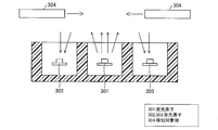
- the reflective sensor includes a light emitting element 301 and two light receiving elements 302 and 303, and the light receiving elements 302 and 303 are arranged on both sides of the light emitting element 301.
- the detection target 304 is on the right side, the reflected light from the detection target 304 strikes the light receiving element 303 strongly.
- the detection target 304 is on the left side, the reflected light from the detection target 304 strikes the light receiving element 302 strongly. Then, the position and movement of the detection object 304 can be detected by reading the difference between the photocurrents generated by the two light receiving elements 302 and 303.
- a sensor that detects the movement of an object to use an optical sensor as a gesture sensor that detects the movement of a hand or the like.
- Such a gesture sensor is used as an additional function for the proximity sensor, and detects the movement of a hand on the touch panel in a non-contact manner. Thereby, even with wet hands or dirty hands, the screen displayed on the liquid crystal panel can be operated without polluting the surface of the liquid crystal panel.
- Patent Document 3 a technique described in Patent Document 3 can be cited as a conventional technique that can detect the moving direction of a detection target with a sensor including one light emitting element and a divided photodiode.
- signals from four light receiving elements each having a multi-layer metal layered on one light emitting element and a four-divided photodiode and having sensitivity directivity in four directions, up and down, and left and right,
- the moving direction of the detection target is detected by taking the difference between the top and bottom and the left and right.
- an electronic device equipped with a light sensor as described above is used outdoors or indoors, it is required to operate correctly even when ambient light from natural light or illumination light enters the light sensor.
- the gesture sensor that detects the movement of the object to be detected is supposed to be used under strong disturbance light such as natural light or illumination light, so it operates correctly when disturbance light from natural light or illumination light enters the optical sensor. It is more strongly required to do this.
- Japanese Patent Publication Japanese Patent Laid-Open No. 2008-8849
- Japanese Patent Publication Japanese Patent Publication “JP-A-2000-75046 (published on March 14, 2000)” US 2012/0280904 (published Nov. 8, 2012)
- the present invention has been made in view of the above-described problems, and an object thereof is to provide an optical sensor that can accurately detect the moving direction of a detection target even when ambient light is present.
- an optical sensor in a ring shape at a light emitting element and an end portion of a region where reflected light obtained by reflecting light emitted from the light emitting element on a detection target is incident.
- a plurality of first light receiving elements that receive the reflected light to generate a photocurrent, and a moving direction detection that receives the photocurrent generated from the first light receiving element and detects the moving direction of the detection object. Means.
- the region where the reflected light which is the light emitted from the light emitting element reflected by the detection target object, changes. This change starts when reflected light begins to enter at the end of the region, and ends when the reflected light ends at the other end of the region. That is, the reflected light that is incident on a portion that is not an end portion of the region does not reflect intrusion / detachment due to the movement of the detection target in the detection range of the optical sensor.
- the plurality of first light receiving elements accurately reflect the intrusion / detachment due to the movement of the detection target in the detection range of the optical sensor.
- the reflected light can be received.
- the optical sensor can detect the moving direction of the detection object.
- the moving direction detecting means receives the photocurrent generated from the first light receiving element, and receives the position of the first light receiving element where the reflected light is incident upon entry of the detection target object into the detection range of the light sensor, and the light.
- the moving direction of the detection object can be detected by comparing the position of the other first light receiving element to which the reflected light is incident when the detection object moves away from the detection range of the sensor.
- the first light receiving element in the region where the reflected light that does not reflect the intrusion / detachment due to the movement of the detection target in the detection range of the optical sensor is present, in the detection of the movement direction of the detection target, It is possible to suppress adverse effects caused by light (disturbance light) incident from the outside of the optical sensor that is not reflected light that is reflected from the detection target.
- FIG. 1 It is a top view which shows the plane structure of the cyclic
- FIG. 5 is a diagram illustrating a state in which an image projected on a divided light receiving element group changes. It is a figure which shows typically operation
- FIG. 10 It is a top view which shows the plane structure of the cyclic
- FIG. 1 It is a block diagram which shows the structure of the integration circuit which concerns on the modification of the integration circuit shown in FIG. It is a top view which shows typically the utilization form of the cyclic
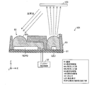
- FIG. 2 is a longitudinal sectional view showing a sectional configuration of the optical sensor 101 according to the embodiment of the present invention.
- the optical sensor 101 includes a light emitting element LED, an annular divided light receiving element group RDPD (a plurality of first light receiving elements), a substrate 91, a transparent resin portion 92, a light shielding resin portion 93, and a gesture circuit.
- Part (movement direction detection means) 32 is provided. Note that the direction of the coordinate axes indicated by XYZ corresponds to the coordinate axes shown in other drawings.
- the annular divided light receiving element group RDPD is arranged in an annular shape as described later at the end of the region where the reflected light reflected by the light emitted from the light emitting element LED and reflected by the detection target 100 is incident. Is received to generate a photocurrent. And the circuit part 32 for gestures detects the moving direction of the detection target object 100 in response to the photocurrent generated from the annular divided light receiving element group RDPD.
- the detection object 100 may be, for example, a finger or a pen that operates a smartphone including the optical sensor 101.
- the light emitting elements LED are mounted on the substrate 91 with a space along with the annular divided light receiving element group RDPD.
- the light emitting element LED is configured by a light emitting diode (LED).
- LED light emitting diode
- the present invention is not limited to this configuration, and a light source other than the light emitting diode may be used as the light emitting element LED.
- the detection object 100 approaches the optical sensor 101, the light emitted from the light emitting element LED is reflected by the detection object 100, and the reflected light is incident on the annular divided light receiving element group RDPD.
- the light emitting element LED outputs an infrared light pulse, and only the signal synchronized with the pulse is detected by the annular divided light receiving element group RDPD.
- the detection object 100 when there is no detection target 100, the light emitted from the light emitting element LED is not reflected from the detection target 100. For this reason, the light incident on the annular divided light receiving element group RDPD is only disturbance light.
- the detection object 100 approaches the optical sensor 101, the light emitted from the light emitting element LED is reflected by the detection object 100, and the reflected light (signal light) and disturbance light enter the annular divided light receiving element group RDPD. Incident.
- the optical sensor 101 can be used as a proximity sensor while being used as a movement direction (gesture) detection sensor of the detection object 100.
- the sum of photocurrents (signal outputs) obtained from the light receiving elements included in the annular divided light receiving element group RDPD may be used as the proximity signal of the detection target 100.
- annular split light receiving element group RDPD The annular divided light receiving element group RDPD is configured by a photodiode, a phototransistor, or OPIC (Optical IC) (registered trademark) in which the annular divided light receiving element group RDPD is integrated with a signal processing circuit and an LED driver circuit. .
- FIG. 1 is a plan view showing a planar configuration of an annular divided light receiving element group RDPD provided in the optical sensor 101 shown in FIG. 2, and FIG. 1A shows the optical sensor 101 detecting the movement of the detection target 100 in the left-right direction.
- (B) is a figure which shows the structure at the time of the optical sensor 101 detecting the vertical movement of the detection target object 100.
- the left-right direction represents the negative or positive direction of the X axis shown in FIG.
- the vertical direction represents the positive or negative direction of the Y axis shown in FIG.
- substrate 91 injects into plane is divided
- the annular divided light receiving element group RDPD is composed of light receiving elements (PDA1, PDA2, PDA4, PDB1 to PDB3, PDC2 to PDC4, PDD1, PDD3, and PDD4) located at the end of the hatched area. .
- the annular divided light receiving element group RDPD has four light receiving elements (PDA3, PDB4, PDC1, PDD2) arranged in the central portion of the region where the reflected light reflected by the light emitted from the light emitting element LED is reflected by the detection target 100. ).
- the annular divided light receiving element group RDPD is divided into an L group (PDB1 to PDB3, PDC2) indicated by the letter “L” in FIG. ⁇ PDC4) and R group (PDA1, PDA2, PDA4, PDD1, PDD3, PDD4) indicated by the letter “R”. Then, using the photocurrent generated from the light receiving elements included in the L group and the photocurrent generated from the light receiving elements included in the R group, the movement of the detection target 100 in the left-right direction is detected.
- the annular divided light receiving element group RDPD is designated as a T group (PDA1, PDA2) indicated by the letter “T” in FIG. , PDA4, PDB1 to PDB3) and D group (PDC2 to PDC4, PDD1, PDD3, PDD4) indicated by the letter “D”. Then, the vertical movement of the detection object 100 is detected using the photocurrent generated from the light receiving elements included in the T group and the photocurrent generated from the light receiving elements included in the D group.
- the relative detection object 100 and the optical sensor 101 are relatively detected. It is possible to detect a positional relationship. Further, by detecting the time change of the position of the detection object 100, the movement speed and the movement direction of the detection object 100 can also be detected.
- the transparent resin portion 92 is formed on the substrate 91 so as to cover the light emitting element LED and the annular divided light receiving element group RDPD.
- the transparent resin portion 92 is formed of a transparent resin material or a visible light cut resin material that transmits a light emission wavelength of the light emitting element LED and cuts a visible light component, and has a light emitting lens portion 92a and a light receiving lens on the surface.
- Part (lens-shaped convex part) 92b see FIG. 2).
- the light emitting lens portion 92a is a convex lens formed so as to form a hemispherical shape on the light emitting side of the light emitting element LED, and focuses light emitted from the light emitting element LED to a predetermined position or converts it into parallel light. Exit.
- the light receiving lens portion 92b is a convex lens formed in a hemispherical shape on the light incident side of the annular divided light receiving element group RDPD, and focuses the light reflected from the detection target 100 on the annular divided light receiving element group RDPD.
- the light receiving lens portion 92b has one focal point located in a region where the reflected light reflected by the light emitted from the light emitting element LED is reflected by the detection target 100, and condenses the reflected light in the region. To do.
- the “region where the reflected light, which is the light emitted from the light emitting element LED reflected by the detection object 100, is incident” is a region on the surface of the substrate 91 on which the annular divided light receiving element group RDPD is arranged.
- the optical sensor 101 can more accurately determine the moving direction of the detection target object 100 even when disturbance light exists. Can be detected.
- the configuration is not limited to the above-described configuration, and the optical sensor 101 may not include the light-emitting lens portion 92a.
- the detection sensitivity in the moving direction of the detection target object 100 depending on the distance between the optical sensor 101 and the detection target object 100 can be obtained. Can be bigger. That is, compared with the case where the optical sensor 101 does not include the light-emitting lens portion 92a, the optical sensor 101 emits light even if the distance between the optical sensor 101 and the detection target object 100 is large and disturbance light is present.
- the optical sensor 101 can change the detectable range (a range extending in a direction parallel to the XY plane in FIG. 1) by including the light emitting lens portion 92a.
- the light shielding resin portion 93 is molded with a light shielding resin so as to cover the outside of the transparent resin portion 92.
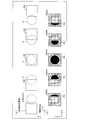
- FIG. 3 is a diagram schematically illustrating the operation of the optical sensor 101 illustrated in FIG. 2, in which (a) corresponds to a state in which the detection target 100 moves in one direction, and (b) corresponds to (a). It is a figure which shows a mode that the image PS projected on the cyclic
- the image PS projected on the annular divided light receiving element group RDPD represents a region where the reflected light, which is the light emitted from the light emitting element LED and reflected by the detection object 100, is incident.
- the detection object 100 is moved in one direction so as to cross the light spot S formed by the light emitted from the light emitting element LED. With the movement, the part of the light spot S reflected by the detection target object 100 changes. Corresponding to the change, the image PS projected on the annular divided light receiving element group RDPD changes as shown in FIG.
- the optical sensor 101 measures the photocurrent generated when the light included in the portion of the light spot S reflected by the detection object 100 is incident on the annular divided light receiving element group RDPD, thereby detecting the detection object 100. Detecting movement. That is, since the optical sensor 101 detects the movement of the detection target 100 by the light included in the light spot S, it may be said that the light spot S is the detection range of the optical sensor 101.
- the image PS is inverted by the light receiving lens portion 92b, and the image PS starts to be projected on the right end portion of the annular divided light receiving element group RDPD as shown in the leftmost diagram of FIG.
- the image PS projected onto the annular divided light receiving element group RDPD spreads and is projected onto the annular divided light receiving element group RDPD as shown in the central view of FIG.
- the size of the image PS to be maximized.
- the region where the reflected light which is the light emitted from the light emitting element LED reflected on the detection target object 100, changes.
- This change starts when reflected light begins to enter at the end of the region, and ends when the reflected light ends at the other end of the region. That is, the reflected light that is incident on the portion that is not the end of the region does not reflect the intrusion / detachment due to the movement of the detection target object 100 in the detection range of the optical sensor 101.
- the light receiving elements included in the annular divided light receiving element group RDPD are annularly arranged at the end of the region, so that the light receiving elements are prevented from entering and leaving due to the movement of the detection object 100 in the detection range of the optical sensor 101.
- the gesture circuit unit 32 receives the photocurrent generated from the light receiving elements included in the annular divided light receiving element group RDPD, and the reflected light is incident upon entering the detection target 100 into the detection range of the optical sensor 101.
- the position of the light receiving element to be detected is compared with the position of another light receiving element to which the reflected light is incident when the detection object 100 moves away from the detection range of the optical sensor 101, and the moving direction of the detection object 100 is detected. can do.
- the optical sensor 101 can detect the moving direction of the detection target object 100.
- the detection target object 100 is arranged. In the detection of the moving direction, the adverse effect caused by the light (disturbance light) incident from the outside of the optical sensor 101 that is not the reflected light reflected by the detection target object 100 from the light emitting element LED can be suppressed.
- the optical sensor 101 can accurately detect the moving direction of the detection target 100 even when disturbance light is present.
- the optical sensor 101 can detect the moving direction of the detection target object more accurately even when disturbance light is present. it can.
- FIG. 4 is a plan view showing a planar configuration of a divided light receiving element group DPD according to a comparative example of the annular divided light receiving element group RDPD shown in FIG.
- the coordinate axes indicated by XY correspond to the coordinate axes shown in FIG.
- the optical sensor 101 includes a divided light receiving element group DPD instead of the annular divided light receiving element group RDPD.
- the region on the substrate 91 where the reflected light which is the light emitted from the light emitting element LED and reflected by the detection target object 100, is divided into four planes.
- a light receiving element (PDA, PDB, PDC, PDD) is arranged in each divided region. And in the said optical sensor, all of these light receiving elements are utilized for the detection of the moving direction of the detection target object 100.
- FIG. 4 is a plan view showing a planar configuration of a divided light receiving element group DPD according to a comparative example of the annular divided light receiving element group RDPD shown in FIG.
- FIG. 5 is a diagram schematically illustrating the operation of the optical sensor according to the comparative example of the optical sensor 101 illustrated in FIG. 2, and (a) illustrates a state in which the detection target 100 moves in one direction.
- These are figures which show a mode that the image PS projected on the division
- coordinate axes indicated by XY correspond to the coordinate axes shown in FIG.
- the image PS projected on the divided light receiving element group DPD represents a region where the reflected light, which is the light emitted from the light emitting element LED and reflected by the detection target object 100, enters.
- the detection target 100 moves in one direction so as to cross the light spot S formed by the light emitted from the light emitting element LED. Yes. With the movement, the part of the light spot S reflected by the detection target object 100 changes. Corresponding to the change, the image PS projected on the divided light receiving element group DPD changes as shown in FIG.
- FIG. 6 is a diagram schematically showing the operation of the divided light receiving element group DPD according to the comparative example shown in FIG. 4, and FIG. 6A is a diagram when the optical sensor detects the movement of the detection target 100 in the left-right direction.
- (B) is a figure which shows a structure when an optical sensor detects the movement of the up-down direction of the detection target object 100.
- FIG. In FIG. 6, coordinate axes indicated by XY correspond to the coordinate axes shown in FIG.
- the left-right direction represents the negative or positive direction of the X axis shown in FIG.
- the vertical direction represents the positive or negative direction of the Y axis shown in FIG.
- the divided light receiving element group DPD is divided into the L group (PDB, PDC) indicated by the letter “L” and the letter “L” in FIG. It is divided into R groups (PDA, PDD) indicated by “R”. Then, using the photocurrent generated from the light receiving elements included in the L group and the photocurrent generated from the light receiving elements included in the R group, the movement of the detection target 100 in the left-right direction is detected.
- the divided light receiving element group DPD is replaced with the T group (PDA, PDB) indicated by the letter “T” in FIG. It is divided into D groups (PDC, PDD) indicated by the letter “D”. Then, the vertical movement of the detection object 100 is detected using the photocurrent generated from the light receiving elements included in the T group and the photocurrent generated from the light receiving elements included in the D group.
- the relative positional relationship between the detection object 100 and the optical sensor including the divided light receiving element group DPD is detected. Further, the movement speed and direction of the detection object 100 are detected by detecting the time change of the position of the detection object 100.
- FIG. 7 is a diagram schematically illustrating an operation when the optical sensor according to the comparative example of the optical sensor 101 illustrated in FIG. 2 detects the movement of the detection target 100.
- a signal as shown in FIG. 7 is obtained.
- four photocurrent output differences X (I_PDA + I_PDD) ⁇ (I_PDB + I_PDC) obtained from the left and right (L, R) of the divided light receiving element group DPD are included in the divided light receiving element group DPD.
- I_PDA represents the value of the photocurrent obtained from the light receiving element PDA.
- I_PDB represents the value of the photocurrent obtained from the light receiving element PDA.
- I_PDB represents the time change of the value of X / Z.
- the principle of detecting the moving direction and moving speed of the detection target in the optical sensor according to the comparative example is as described above, but in reality, disturbances such as artificial lighting and sunlight There is light, and it is necessary to operate without malfunction even under the disturbance light.
- the optical sensor according to Comparative Example 1 In the optical sensor according to Comparative Example 1, all of the light receiving elements included in the divided light receiving element group DPD are used for detecting the moving direction of the detection target object 100.
- the detection target object is used in the optical sensor 101.
- the light receiving elements used for detecting the moving direction of 100 are limited to light receiving elements arranged in an annular shape at the end of the region where the reflected light, which is the light emitted from the light emitting element LED reflected by the detection object 100, enters.
- the optical sensor 101 does not use a light receiving element arranged in a region where reflected light that does not reflect intrusion / detachment due to movement of the detection object 100 in the detection range of the optical sensor 101 is incident.
- the optical sensor 101 in detection of the moving direction of the detection target object 100, light (disturbance light) incident from the outside of the optical sensor 101 that is not reflected light reflected from the detection target object 100 by the light emitted from the light emitting element LED. Compared with the optical sensor which concerns on the comparative example 1, the bad influence resulting from can be suppressed.
- the ratio (X / Z, Y / Z) of the left / right (L, R) or upper / lower (T, D) difference output signals, which are direction detection signals, is the edge of the detection object 100.
- the maximum value is output when Therefore, even if the light receiving element (PDA3, PDB4, PDC1, PDD2) at the center of the annular divided light receiving element group RDPD provided in the optical sensor 101 as shown in FIG. Since there is no change in the portion where the ratio signal has a large value (1 or -1), the direction detection accuracy is not deteriorated. Therefore, the optical sensor 101 can suppress malfunction under ambient light while maintaining the direction detection accuracy of the detection target.
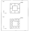
- FIG. 8 is a plan view showing a planar configuration of an annular divided light receiving element group according to a modification of the annular divided light receiving element group RDPD shown in FIG. 1, wherein (a) is an annular divided light receiving element including four light receiving elements. (B) is a figure which shows the cyclic
- the configuration of the light receiving elements included in the annular divided light receiving element group RDPD may be configured as shown in FIG. 8 (a) or FIG. 8 (b).
- FIG. 8A shows an annular divided light receiving element group RDPa composed of L-shaped light receiving elements (first light receiving elements) PD1 to PD4, and FIG.
- the optical sensor 101 has a configuration in which the annular divided light receiving element group RDPD shown in FIG. 1 is changed to an annular divided light receiving element group RDPDa shown in FIG. 8A or an annular divided light receiving element group RDPDb shown in FIG. There may be. That is, in the optical sensor 101, the shape of the light receiving element included in the annular divided light receiving element group RDPD can be arbitrarily selected, and the annular divided light receiving element group RDPD can be configured by light receiving elements of various shapes.
- the shape of the light receiving element included in the annular divided light receiving element group RDPD according to the shape of the region where the reflected light reflected by the detection object 100 is emitted from the light emitting element LED, For example, the amount of reflected light reflected by the detection object 100 can be maximized, or disturbance light can be minimized.
- FIG. 9 is a schematic diagram showing a configuration of an optical sensor 104 according to another embodiment of the present invention.
- the optical sensor 104 includes a register 3A, an I2C interface 4, an integration control circuit (integration control means) 5, an oscillator 6, a drive signal generation circuit 7, and a drive circuit (drive means) 8. .
- An integrating circuit (integrating means) 10 of the circuit unit 31 and an AD converter 20 are provided.
- the optical sensor 104 has the same configuration as the optical sensor 101.
- the output voltages of the integrating circuits 10 to 14 are converted into digital data by the AD converters 20 to 24, respectively, and the converted data are stored in the register 3A.
- the digital data stored in the register 3A can be taken out by the I2C interface 4.
- an LED drive signal is generated by a reference clock from the oscillator 6, and a pulse current is generated by the drive circuit 8, causing the light emitting element LED to emit light and outputting an optical pulse signal.
- the annular divided light receiving element group RDPD (light receiving elements PDA1, PDA2, PDA4, PDB1 to PDB3, PDC2 to PDC4, PDD1, PDD3, PDD4) is used for detecting the movement direction (gesture) of the detection object 100, and the annular divided light receiving is performed.
- the light receiving elements (second light receiving elements) PDA3, PDB4, PDC1, and PDD2 are also arranged in the area (center) of the area where the element group RDPD is arranged, and are used for illuminance detection.
- An integrated photosensor is realized.
- the optical sensor 104 includes, in addition to the configuration of the optical sensor 101, the light receiving elements PDA3, PDB4, PDC1, and PDD2 disposed in the end region where the annular divided light receiving element group RDPD is disposed.
- An illuminance circuit unit 31 is further provided for detecting the illuminance by receiving the photocurrent generated from the elements PDA3, PDB4, PDC1, and PDD2.
- FIG. 10 is a block diagram showing the configuration of the integrating circuits 10, 11, 12, 13 and 14 in the optical sensor 104 shown in FIG.
- each integrating circuit includes a capacitor (integrating means) C1.
- the capacitor C1 is charged by receiving the photocurrent generated from the annular divided light receiving element group RDPD, and discharges the charge as an integral value.
- the charge / discharge is controlled by a charge / discharge control unit (integral control means) 40.
- the charge / discharge control unit 40 may be the integration control circuit 5 shown in FIG.
- the integration circuits 10, 11, 12, 13, and 14 are capacitors C1 that are charged / discharged by charges corresponding to the magnitude of the photocurrent, and the charge / discharge control unit 40 Control charging / discharging of the capacitor C1. Further, as will be described later, the charge / discharge control unit 40 charges or discharges the capacitor C1 during a period in which the light emitting element LED is lit, and the capacitor during a period in which the light emitting element LED is not lit. C1 may be discharged or charged to control charge / discharge of the capacitor C1.
- the integration circuits 10, 11, 12, 13 and 14 can be realized with a simple configuration in which the capacitor C1 is charged and discharged by the photocurrent generated from the light receiving element. That is, the optical sensor 104 can be manufactured at low cost.
- the optical sensor 104 can detect the moving direction of the detection target object even more accurately even when ambient light is present, and can reduce the cost of the optical sensor 104.
- FIG. 11 is a block diagram showing a configuration of another integrating circuit 1 in the optical sensor 104 shown in FIG.
- the integration circuits 10 to 14 described above may be replaced with one integration circuit 1 as shown in FIG.
- the integrating circuit 1 includes an input switching circuit 1a, integrators 1ba to 1bd, delay circuits 1da to 1dc, and an adding circuit 1e.
- Integrators 1ba and 1bd are circuits that integrate the input photocurrent in the negative (or positive) direction.
- the integrators 1bb and 1bc are circuits that integrate the input photocurrent in the positive (or negative) direction.
- the input switching circuit 1a is a circuit that switches the input path in four consecutive integration periods so that the photocurrent from the annular divided light receiving element group RDPD is input to any one of the integrators 1ba to 1bd.
- the input switching circuit 1a is controlled so as to switch the input of the photocurrent by the integration control signal given from the integration control circuit 5 described above.
- the integration control signal defines four integration periods INT1 to INT4 for executing integration, which will be described later, and also defines an integration period in which the integration periods INT1 to INT4 are one period.
- the integration periods INT1 to INT4 are periods in which the light emitting elements LED are turned on (turned on) and turned off (turned off), respectively, which are a first period T1, a second period T2, a third period T3, and a fourth period T4, which will be described later. Is provided.
- Delay circuits 1 da to 1 dc are circuits that delay the integration values output from the integrators 1 ba to 1 bc for 3 to 1 integration periods, respectively.
- the adder circuit 1e is a circuit that adds the integrated values output from the delay circuits 1da to 1dc and the integrator 1bd.
- the photocurrent is negative or negative by the integrators 1ba and 1bd. Integrated in the positive direction.
- the integration value output from the integrator 1ba is delayed by three integration periods by the delay circuit 1da.
- the photocurrent is integrated in the positive or negative direction by the integrators 1bb and 1bc.
- the integration values output from the integrators 1bb and 1bc are delayed by 2 and 1 integration periods by the delay circuits 1db and 1dc, respectively.
- FIG. 12 is a block diagram showing a configuration of an integration circuit 1A according to a modification of the integration circuit 1 shown in FIG.
- the integration circuit 1 described above may be an integration circuit 1A as shown in FIG.
- the integrating circuit 1A includes a current polarity switching circuit 1Aa, an integrator 1Ab, an output switching circuit 1Ac, delay circuits 1Ada to 1Adc, and an adding circuit 1Ae.
- the current polarity switching circuit 1Aa is a circuit that switches the polarity of the photocurrent from the annular divided light receiving element group RDPD in four consecutive integration periods.
- the current polarity switching circuit 1Aa is controlled to switch the polarity of the photocurrent by the integration control signal.
- the integrator 1Ab is a circuit that integrates the photocurrent output from the current polarity switching circuit 1Aa.
- the output switching circuit 1Ac is a circuit that alternately switches output paths in four consecutive integration periods so that the integration value output from the integrator is output to any one of the delay circuits 1Ada to 1Adc and the addition circuit 1Ae. is there.
- the output switching circuit 1Ac is controlled to switch the output path by the integration control signal.
- Delay circuits 1Ada to 1Adc are circuits that delay the integration value output from the output switching circuit 1Ac for 1 to 3 integration periods.
- the adder circuit 1Ae is a circuit that adds the integrated values output from the delay circuits 1Ada to 1Adc and the output switching circuit 1Ac.
- the integrating circuit 1A configured as described above, when a photocurrent is output as a negative (or positive) photocurrent from the current polarity switching circuit 1Aa, the photocurrent is integrated by the integrator 1Ab.
- the integral value output from the integrator 1Ab is output directly to the adder circuit 1Ae via the output switching circuit 1Ac and not via the delay circuit.
- the integral value is output to the delay circuit 1Adc via the output switching circuit 1Ac, delayed by three integration periods by the delay circuit 1Adc, and output to the adder circuit 1Ae.
- the photocurrent is integrated by the integrator 1Ab.
- the integrated value output from the integrator 1Ab is output to the delay circuit 1Ada via the output switching circuit 1Ac, delayed by one integration period by the delay circuit 1Ada, and output to the adder circuit 1Ae.
- the integrated value is output to the delay circuit 1Adb via the output switching circuit 1Ac, delayed by two integration periods by the delay circuit 1Adb, and output to the adder circuit 1Ae.
- the integration value of the integration periods INT3 to INT1 output from the delay circuits 1Ada to 1Adc and the integration value of the integration period INT4 output from the output switching circuit 1Ac are added by the addition circuit 1Ae. In this way, by adding the integral value of the positive photocurrent and the integral value of the negative photocurrent, an integral value of the difference between the two integral values is obtained.
- Such an integration circuit 1A can output an integration value equivalent to that of the integration circuit 1 shown in FIG. Further, unlike the integration circuit 1 having four integrators 1ba to 1bd, the integration circuit 1A has one integrator 1Ab, so that the circuit configuration can be simplified.
- the AD converters 20 to 24 shown in FIG. 9 are circuits that convert the integrated values output from the integrating circuits 10 to 14 (integrating circuits 1 and 1A) into digital values, respectively.
- the AD converters 20 to 24 convert the sum of the integration values in the positive or negative direction of the integration periods INT1 to INT4 output from the integration circuits 10 to 14 (integration circuits 1 and 1A) into digital digital integration values. Output.
- the I2C interface 4 is a circuit that outputs a digital value output from the register 3A as serial data SDA in synchronization with an external serial clock SCL.
- the oscillator 6 is a circuit that generates a reference clock having a predetermined period.
- the integration control circuit 5 Based on the reference clock from the oscillator 6, the integration control circuit 5 outputs an integration control signal that becomes high level in each of the integration periods INT1 to INT4 in which integration is performed and becomes low level in the non-integration period in which integration is not performed.
- Integration periods INT1 to INT4 to be described later are set as periods shorter than first to fourth periods T1 to T4 to be described later in which the light emitting element LED is turned on or off.
- the drive signal generation circuit 7 is a circuit that generates a drive signal for driving the light emitting element LED based on the reference clock from the oscillator 6.
- This drive signal is a signal for turning on and off the light emitting element LED in a cycle having the first period T1, the second period T2, the third period T3, and the fourth period T4 as a unit.
- the first to fourth periods T1 to T4 correspond to the on period and the off period.
- the light emitting element LED is driven so that the light emitting element LED is turned off in the first period T1 and the fourth period T4 and turned on in the second period T2 and the third period T3.
- the light emitting element LED is not limited to such drive control, and is turned on in the first period T1 and the fourth period T4 and turned off in the second period T2 and the third period T3, contrary to the above-described configuration. May be driven.
- the drive circuit 8 is a circuit that generates a drive current for driving the light emitting element LED based on the drive signal generated by the drive signal generation circuit 7.
- This drive current is a pulse current, and is given to the light emitting element LED as an optical pulse signal.
- the light sensor 104 is received by the light receiving elements PDA3, PDB4, PDC1, and PDD2, and the illuminance is detected by the illuminance circuit unit 31. It can be used for proximity sensors.
- one of the focal points is located in a region where the reflected light reflected by the detection target 100 is incident, and the light sensor 104 includes a light receiving lens portion 92b (see FIG. 2) that collects the reflected light in the region.
- the light receiving lens portion 92b is arranged so that the reflected light is condensed on the light receiving elements PDA3, PDB4, PDC1, and PDD2, thereby efficiently transmitting light (illuminance signal) outside the optical sensor 104. It can receive light. That is, the light receiving elements PDA3, PDB4, PDC1, and PDD2 are arranged directly below the center of the light receiving lens portion 92b as shown in FIG. 2, and can efficiently receive the illuminance signal.
- the optical sensor 104 can accurately detect the moving direction of the detection target object 100 even in the presence of disturbance light, and the optical sensor 104 can be an illuminance sensor, an RGB color sensor, a proximity sensor, and the like. It can be used as a sensor.
- one of the focal points is located in a region where the reflected light reflected by the detection object 100 is incident, and the light sensor 104 includes a light receiving lens portion 92b (see FIG. 2) that collects the reflected light in the region.
- the optical sensor 104 can accurately detect the moving direction of the detection target object 100 even in the presence of disturbance light, and the optical sensor 104 can be used as an illuminance sensor, an RGB color sensor, or a proximity sensor. Can be suitably used.
- FIG. 13 is a plan view schematically showing a usage form of the annular divided light receiving element group RDPD in the optical sensor 104a according to another embodiment of the present invention, in which FIG. 13A shows a form using 12 light receiving elements.
- FIG. 13A shows a form using 12 light receiving elements.
- (B) is a figure which shows the form using eight light receiving elements,
- (c) is a figure which shows the form using four light receiving elements.
- FIG. 14 is a schematic diagram showing a configuration of an optical sensor 104a according to another embodiment of the present invention.
- the optical sensor 104a has the same configuration as that of the optical sensor 104 shown in FIG. 9, except that the input line from each light receiving element (light receiving area) included in the annular divided light receiving element group RDPD is the light receiving area.
- the signal is input to a switching circuit (photocurrent selection means) 50, and a signal from an arbitrary light receiving element is input to the integrating circuits 10-14.
- a switching circuit photocurrent selection means 50
- a signal from an arbitrary light receiving element is input to the integrating circuits 10-14.
- FIG. 13B four photocurrents (current signals) from the light receiving elements PDA2 + PDB1, PDB3 + PDC2, PDC4 + PDD3, PDD1 + PDA4, and as shown in FIG.
- Photocurrents generated from the four-angle light receiving elements (PDA1, PDB2, PDC3, PDD4) are input to the integrating circuits 11 to 14, respectively.
- the optical sensor 104a further includes a light receiving region switching circuit 50 that selects a photocurrent to be applied to the gesture circuit unit 32 from a plurality of photocurrents generated in the annular divided light receiving element group RDPD.
- the light receiving region switching circuit 50 selects a photocurrent to be applied to the gesture circuit unit 32.
- the circuit part 32 for gesture can selectively utilize only the specific light receiving element contained in the cyclic
- a photocurrent resulting from the movement of the detection target object 100 may occur only in some of the light receiving elements. Therefore, the gesture circuit unit 32 selectively uses only a light receiving element that generates a photocurrent due to the movement of the detection target object 100, thereby detecting the movement direction of the detection target object 100.
- the S / N Signal to Noise ratio
- the current signal used for the gesture determination is small, but the disturbance light component is further reduced by the amount of the light receiving region, so that the optical system of the optical sensor 104a and the positions of the optical sensor 104a and the detection object 100 are also reduced.
- the overall S / N can also be increased.
- the optical sensor 104a may further include a register 3A that holds information on the annular divided light receiving element group RDPD that generates a photocurrent selected by the light receiving region switching circuit 50.
- the light receiving region switching circuit 50 can select the photocurrent at high speed with reference to the register 3A even if the positional relationship between the optical sensor 104a and the detection object 100 changes. Following this, only a light receiving element that generates a photocurrent resulting from the movement of the detection target 100 can be selectively and accurately used.
- the light receiving region switching circuit 50 acquires information on the annular divided light receiving element group RDPD from the register 3A via the input line 51, and selects a photocurrent.
- the optical sensor 104a can detect the moving direction of the detection target object 100 more accurately even when disturbance light is present.
- the optical sensor 104a can accurately detect the moving direction of the detection target object 100 in accordance with the change in the positional relationship between the optical sensor 104a and the detection target object 100.
- Embodiments 1 to 3 described above are techniques that are particularly effective when disturbance light does not change (the disturbance light can also be expressed as direct current (DC)), but the light emitted from the light emitting element is detected. If the disturbance light changes during the detection period of the reflected light reflected by the object, the movement direction of the detection object cannot be accurately detected due to the change, and there is a possibility of malfunction.
- a lighting fixture particularly an inverter fluorescent lamp can be cited as an example.
- the brightness of light from ordinary lighting fixtures changes at a frequency (100 Hz or 120 Hz) that is twice the commercial frequency (50 Hz or 60 Hz).
- the light waveform of the inverter fluorescent lamp is a light waveform in which a frequency of several tens of kHz is superimposed on the commercial frequency.
- the light sensor detects the moving direction of the detection target. In many cases, the light intensity of disturbance light changes with time.
- disturbance light that does not change at high speed, such as sunlight
- the disturbance DC light is blocked by the movement of the detection object, and the disturbance light is incident on the optical sensor.
- the light has changed (a situation equivalent to a change in ambient light).
- the movement of the detection object is at a constant speed, it is considered that such disturbance light changes so as to decrease at a constant speed or increase at a constant speed.
- constant decrease or constant increase such constant light decrease or constant speed increase will be referred to as constant decrease or constant increase.
- a photocurrent value integration form capable of canceling the disturbance light is shown. The integration in this form is performed by the integration circuits 10 to 14 shown in FIG. 9 or FIG.
- FIG. 15 is a timing chart showing an integrated form of photocurrent values according to another embodiment of the present invention.
- FIG. 15 shows a situation in which the photocurrent caused by disturbance light is constantly reduced. As shown in FIG. 15, the light emitting element on period and the light emitting element off period are repeated, the photocurrent generated in the light receiving element in the light emitting element on period is integrated in the positive direction, and the light generated in the light receiving element in the light emitting element off period. The current is integrated in the negative direction.
- the disturbance light does not change (when the disturbance light is DC light)
- the photocurrent caused by the disturbance light can be completely canceled by such an integration form.
- the light emitting element off period (T1), the light emitting element on period (T2), the light emitting element on period (T3), and the light emitting element off period (T4) are one cycle.
- integration is performed in the negative direction (INT1) in the first light emitting element off period (T1), and integration is performed in the positive direction (INT2) in the next light emitting element on period (T2).
- a negative output remains.
- the periods of INT3 and INT4 are positive.
- the component due to the reflected light from the object to be detected is obtained by repeating the integration of several cycles with the light emitting element off period, the light emitting element on period, the light emitting element on period, and the light emitting element off period as one period. Can only be integrated.
- the period of the integration period and the period of the on / off period of the light emitting element may be, for example, 50 kHz or more in terms of frequency, or may be a higher frequency.
- the disturbance light is constantly reduced without using complicated signal calculation or the like.
- the disturbance light can be canceled.
- even when disturbance light increases by a certain amount by the integration form, the disturbance light can be canceled.
- the one cycle is a light emitting element on period, a light emitting element off period, a light emitting element off period, and a light emitting element on period, disturbance light that is similarly reduced or increased can be canceled.
- the optical sensor 104 illustrated in FIG. 9 or the optical sensor 104a illustrated in FIG. 14 includes the first period and the fourth period in the first period T1, the second period T2, the third period T3, and the fourth period T4.
- the light emitting element in a period is turned on or off, and a driving circuit (driving means) 8 that drives the light emitting element to be turned off or turned on in the second period and the third period, and the value of the photocurrent is
- the integration circuits (integration means) 10 to 14 for integration and the light emitting element LED are turned off so that the integration circuits 10 to 14 integrate in the positive or negative direction during the period when the light emitting element LED is on.
- the integration control circuit (integration control means) 5 for controlling the integration circuits 10 to 14 is controlled so that the integration circuits 10 to 14 integrate in the negative or positive direction during the turn-off period. It may be provided to.
- the light (disturbance light) which enters from the exterior of the optical sensor which is not the reflected light which the emitted light of light emitting element LED reflected on the detection target object 100 follows a continuous 1st period, 2nd period, 3rd.
- the integration control circuit 5 performs integration so that the value obtained by integrating the photocurrent values caused by the disturbance light becomes 0 when the integration control circuit 5 is constantly decreased or increased.
- the circuits 10 to 14 can be controlled.
- the optical sensor 104 or the optical sensor 104a can remove an adverse effect caused by disturbance light that is constantly decreased or increased in detection of the moving direction of the detection object 100. That is, the optical sensor 104 or the optical sensor 104a can cancel disturbance light that is constantly decreasing or increasing.
- the optical sensor 104 or the optical sensor 104a can detect the moving direction of the detection target object even more accurately even when there is disturbance light that constantly decreases or increases.
- the integration circuits 10 to 14 are capacitors C1 that are charged and discharged by a charge corresponding to the magnitude of the photocurrent as shown in FIG. 10, and the integration control circuit 5 is a charge and discharge control unit 40.
- the capacitor C1 is charged or discharged during the period when the light emitting element LED is turned on, and the capacitor C1 is discharged or charged during the period when the light emitting element LED is turned off to charge / discharge the capacitor C1. You may control.
- the integration circuits 10 to 14 can be realized with a simple configuration in which the capacitor C1 is charged and discharged by the photocurrent generated from the light receiving element. That is, the optical sensor 104 or the optical sensor 104a can be manufactured at low cost.
- the optical sensor 104 or the optical sensor 104a can detect the moving direction of the detection target 100 even more accurately even when there is disturbance light that constantly decreases or increases, and the optical sensor 104 or the optical sensor.
- the cost of 104a can be reduced.
- the gesture circuit unit 32 is connected to the annular divided light receiving element group RDPD that generates a photocurrent due to the movement of the detection target 100.
- the photocurrent to be used can be reduced and the charge / discharge amount of the capacitor C1 can be reduced. This eliminates the need for the optical sensor to use a large capacity as an integrating circuit.
- the optical sensor 104 or the optical sensor 104a can detect the moving direction of the detection target 100 even more accurately even when there is disturbance light that constantly decreases or increases, and the optical sensor 104 or the optical sensor.
- the cost of 104a can be further reduced.
- FIG. 16 is a timing chart showing an integration form according to a comparative example of the integration form of the photocurrent values shown in FIG.
- the light emitting element on period (T1), the light emitting element off period (T2), the light emitting element on period (T3), and the light emitting element off period (T4) are set to 1. It is a cycle. Therefore, under the condition that the disturbance light is constantly reduced, integration in the positive direction (INT1) is performed in the first light emitting element on period (T1), and integration in the negative direction (INT2) in the next light emitting element off period (T2). The remaining positive output remains in the final integrated value.
- the disturbance light component is always larger during the light-emitting element ON period, so the photocurrent increases, and the signal component due to the photocurrent caused by the reflected light from the detection target Even if there is no signal, the output is as if the signal is present.
- FIG. 17 is a timing chart showing an integration mode according to another comparative example of the photocurrent value integration mode shown in FIG.
- the light emitting element is turned off in the first period T1, the second period T2, and the fourth period T4, while the light emitting element is turned on in the third period T3.
- ADC1 which is a difference between integrated values of photocurrents of the light receiving elements generated according to the respective states of the light emitting elements in the first period T1 and the second period T2
- ADC2 which is a difference between integrated values of photocurrents generated according to the respective states of the light emitting elements in T3 and the fourth period T4
- the register control circuit determines that the integral value ADC1 is positive, reads the integral values ADC1 and ADC2 from a register (not shown), and subtracts the integral value ADC1 from the integral value ADC2 by a not-shown register, The increment of the integral value ADC2 is canceled from the integral value ADC1.
- the integral form shown in FIG. 15 requires complicated signal calculation and configuration as in the integral form shown in FIG. 17 only by changing the light emission timing of the light emitting element (for example, off, on, on, off). Even if the disturbance light fluctuates, the disturbance light can be canceled.
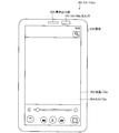
- FIG. 18 is a schematic diagram showing a configuration of a smartphone (electronic device) 201 according to another embodiment of the present invention.
- a smartphone 201 as an electronic device is configured by incorporating a liquid crystal panel 203 and a touch panel 204 in a housing 202.
- the liquid crystal panel 203 is provided on the operation surface side of the housing 202.
- the touch panel 204 is provided on the liquid crystal panel 203.
- the audio output unit 205 and the optical sensors 101, 104, or 104a are arranged on the upper part of the operation surface of the housing 202.
- the audio output unit 205 is provided for outputting audio when using the smartphone 201 as a telephone and various sounds according to the operation of the application program.
- the optical sensors 101, 104, or 104a are optical sensors provided for detecting the proximity of the detection object 100 (for example, the user's face) or detecting a gesture operation.
- the smartphone 201 includes any one of the optical sensors 101, 104, or 104a.
- the smartphone 201 includes any one of the optical sensors 101, 104, or 104a, so that the detection target 100 is affected by disturbance light even when used in an environment where disturbance light is generated.
- the position and movement of the detection target object 100 can be accurately detected without receiving.
- the optical sensors 101, 104, or 104a can be implemented.
- various electronic devices such as digital cameras and car navigation systems as well as smartphones, even if ambient light is present in these electronic devices, the detection target A sensing function that can accurately detect the moving direction of an object can be implemented.
- the light emitting element off period, the light emitting element on period, the light emitting element on period, and the light emitting element off period are one cycle, or the light emitting element on period, the light emitting element off period, the light emitting element off period, and the light emitting element on period.
- the integration of several cycles is repeated with the period as one cycle. That is, four periods are defined as one cycle.
- the present invention is not limited to the configuration in which the four periods are one cycle.
- n is an integer of 2 or more
- 2n consecutive periods are defined as one period, and the intermediate point of period integration (the nth period Tn and the n + 1th period).
- Tn the intermediate point of period integration
- FIG. 19 is a timing chart showing an integrated form of photocurrent values according to another embodiment of the present invention.
- the light emitting element off period and the light emitting element on period are repeated until the intermediate point of the period integration (period group P1), and the light emitting element on period after the intermediate point of the period integration (period group P2).
- the light emitting element off period is repeated.
- the present invention is not limited to this configuration.
- the light emitting element on period and the light emitting element off period are repeated up to the intermediate point of the period integration, and the light emitting element off period and the light emitting element on period are started from the intermediate point onward of the period integration. May be repeated.
- the “period group” means a period including a plurality of light-emitting element on periods and / or a plurality of light-emitting element off periods.
- 2n integration periods INT1, INT2 to INTn-1, INTn, INTn + 1, INTn + 2 to INT2n-1 and INT2n for performing integration are defined, and an integration period with one integration period INT1 to INT2n is also defined. It prescribes.
- the integration periods INT1 to INT2n are periods in which the light emitting elements LED are turned on (turned on) and turned off (lights off), respectively.
- the optical sensor 104 shown in FIG. 9 or the optical sensor 104a shown in FIG. 14 turns off or turns on the light emitting element LED in the first period T1 in 2n consecutive periods, where n is an integer of 2 or more.
- the light-emitting element LED is driven to be turned on or off, and a period group P1 including the first period T1 to the n-th period Tn and a period including the n + 1 period to the 2n-th period.
- the circuits (integrating means) 10 to 14 and the integrating circuits 10 to 14 are positive or negative while the light emitting element LED is on.
- An integration control circuit that controls the integration circuits 10 to 14 so that the integration circuits 10 to 14 integrate in the negative or positive direction during the extinguishing period when the light emitting element LED is turned off so as to integrate in the direction. (Integral control means) 5 may be further provided.
- the light (disturbance light) which enters from the outside of the optical sensor which is not the reflected light which the emitted light of light emitting element LED reflected on the detection target object 100 reduces or stops constant in 2n continuous periods.
- the integration control circuit 5 can control the integration circuits 10 to 14 so that the value obtained by integrating the photocurrent values caused by the disturbance light by the integration circuits 10 to 14 becomes zero.
- the optical sensor 104 or the optical sensor 104a can remove an adverse effect caused by disturbance light that is constantly decreased or increased in detection of the moving direction of the detection object 100. That is, the optical sensor 104 or the optical sensor 104a can cancel disturbance light that is constantly decreasing or increasing.
- the continuous 2n periods are configured by repeating the light emitting element off period and the light emitting element on period, or repeating the light emitting element on period and the light emitting element off period. Will not be long. Accordingly, even when disturbance light (noise) that changes at high speed is incident on the optical sensor 104 or the optical sensor 104a, the optical sensor 104 or the optical sensor 104a follows the change, and the optical sensor 104 or the optical sensor 104a Movement can be accurately detected.
- the optical sensor 104 or the optical sensor 104a can detect the moving direction of the detection target object even more accurately even when there is disturbance light that constantly decreases or increases.
- the gesture circuit section 32, the illuminance circuit section 31, the light receiving area switching circuit 50, the drive circuit 8, the integration circuits 10 to 14, 1, 1A and the integration control circuit 5 of the optical sensor 101, 104 or 104a are integrated circuits (IC It may be realized by a logic circuit (hardware) formed on a chip) or the like, or may be realized by software using a CPU (Central Processing Unit).
- IC integrated circuits
- CPU Central Processing Unit
- the optical sensor 101, 104, or 104a includes a CPU that executes instructions of a program that is software that realizes each function, and a ROM (Read that records the program and various data so that the computer (or CPU) can read them And a storage device (these are referred to as “recording media”), a RAM (Random Access Memory) for expanding the program, and the like. Then, the computer (or CPU) reads the program from the recording medium and executes it to achieve the object of the present invention.
- a “non-temporary tangible medium” such as a tape, a disk, a card, a semiconductor memory, a programmable logic circuit, or the like can be used.
- the program may be supplied to the computer via an arbitrary transmission medium (such as a communication network or a broadcast wave) that can transmit the program.
- a transmission medium such as a communication network or a broadcast wave
- the present invention can also be realized in the form of a data signal embedded in a carrier wave, in which the program is embodied by electronic transmission.
- the photosensors (101, 104, 104a) according to the first aspect of the present invention are annularly arranged at the end of the region where the light emitting element LED and the reflected light reflected by the detection target object 100 from the light emitted from the light emitting element are incident.
- the plurality of first light receiving elements annular divided light receiving element group RDPD
- receive the reflected light and generate a photocurrent, and the photocurrent generated from the first light receiving element And a moving direction detecting means (the gesture circuit unit 32) for detecting the moving direction.
- the region where the reflected light which is the light emitted from the light emitting element reflected by the detection target, changes.
- This change starts when reflected light begins to enter at the end of the region, and ends when the reflected light ends at the other end of the region. That is, the reflected light that is incident on a portion that is not an end portion of the region does not reflect intrusion / detachment due to the movement of the detection target in the detection range of the optical sensor.
- the plurality of first light receiving elements in an annular shape at the end of the region, the plurality of first light receiving elements accurately reflect the intrusion / detachment due to the movement of the detection target in the detection range of the optical sensor.
- the moving direction detecting means receives the photocurrent generated from the first light receiving element, and the position of the first light receiving element where the reflected light enters when the detection target moves into the detection range of the light sensor and the light is detected.
- the moving direction of the detection object can be detected by comparing the position of the other first light receiving element to which the reflected light is incident when the detection object moves away from the detection range of the sensor.
- the optical sensor can detect the moving direction of the detection target.
- the first light receiving element in the region where the reflected light that does not reflect the intrusion / detachment due to the movement of the detection target in the detection range of the optical sensor is present, in the detection of the movement direction of the detection target, It is possible to suppress adverse effects caused by light (disturbance light) incident from the outside of the optical sensor that is not reflected light that is reflected from the detection target.
- the optical sensor can accurately detect the moving direction of the detection target even when disturbance light is present.
- the optical sensor according to aspect 2 of the present invention is the optical sensor according to aspect 1, wherein one of the focal points is located in a region where the reflected light is incident, and a lens-shaped convex portion (light receiving portion) that collects the reflected light in the region.
- a lens portion 92b) may be provided.
- the optical sensor since the reflected light reflected on the detection target can be collected by the lens-shaped convex portion, the optical sensor can detect the moving direction of the detection target more accurately even when disturbance light exists. can do.
- An optical sensor according to aspect 3 of the present invention is the optical sensor according to aspect 1 or 2, wherein the second light receiving element (light receiving element PDA3) arranged in an area inside the end region where the plurality of first light receiving elements are arranged in an annular shape. , PDB4, PDC1, PDD2) and illuminance detection means (illuminance circuit unit 31) for detecting the illuminance by receiving the photocurrent generated from the second light receiving element.
- the second light receiving element light receiving element PDA3
- PDC1, PDD2 illuminance detection means for detecting the illuminance by receiving the photocurrent generated from the second light receiving element.
- the light sensor is used for an illuminance sensor, an RGB color sensor, a proximity sensor, etc. by receiving light incident from the outside of the optical sensor by the second light receiving element and detecting the illuminance by the illuminance detection means. be able to.
- the optical sensor can accurately detect the moving direction of the detection target even when disturbance light is present, and the optical sensor can be used for an illuminance sensor, an RGB color sensor, a proximity sensor, and the like. .
- the optical sensor when one of the focal points is located in a region where the reflected light reflected by the detection target is incident, and the optical sensor includes a lens-shaped convex portion that collects the reflected light in the region.
- the lens-shaped convex portion By arranging the lens-shaped convex portion so that the reflected light is condensed on the second light receiving element, it is possible to efficiently receive light (illuminance signal) incident from the outside of the optical sensor.
- the optical sensor can accurately detect the moving direction of the detection target even in the presence of disturbance light, and can be suitably used for an illuminance sensor, an RGB color sensor, a proximity sensor, and the like. it can.
- the optical sensor according to Aspect 4 of the present invention is the optical sensor according to any one of Aspects 1 to 3, wherein the photocurrent applied to the moving direction detection means from the plurality of photocurrents generated in the first light receiving element is the disturbance light.
- Photocurrent selecting means for selecting according to the intensity may be further provided.
- the photocurrent selection means selects the photocurrent to be given to the moving direction detection means.
- the movement direction detection means can selectively use only the specific first light receiving element.
- a photocurrent resulting from the movement of the detection target may occur only in some of the first light receiving elements. Therefore, the moving direction detection means selectively uses only the first light receiving element that generates a photocurrent due to the movement of the detection target object, thereby detecting the light emitted from the light emitting element in detecting the movement direction of the detection target object.
- the optical sensor can detect the moving direction of the detection target object more accurately.
- the magnitude of the photocurrent generated in the first light receiving element varies depending on the optical system that makes light incident on the first light receiving element and the sensitivity or size of the first light receiving element.
- the photocurrent selecting means selects the photocurrent to be given to the moving direction detecting means from the plurality of photocurrents generated in the first light receiving element according to the intensity of the disturbance light” means that the light is applied to the first light receiving element. In other words, it can be selected depending on the optical system to be incident, and it can also be selected in accordance with the sensitivity or size of the first light receiving element.
- a saturation phenomenon of an integrating circuit due to excessive photocurrent can be mentioned.
- a plurality of photocurrents generated in the first light receiving element may be used for an operation of integrating the values by an integration circuit.
- the integration circuit executes the integration operation assuming that the photocurrent value remains at the certain value. May end up.
- Such a phenomenon is called an integration circuit saturation phenomenon.
- the photocurrent selection means moves in the direction of movement from the plurality of photocurrents generated in the first light receiving element.
- the photocurrent applied to the detection means can be selected so that the integration circuit does not saturate. That is, “the photocurrent selection means selects the photocurrent to be given to the moving direction detection means from the plurality of photocurrents generated in the first light receiving element according to the intensity of the disturbance light” does not cause saturation of the integration circuit. It can be paraphrased to select as follows.
- the photocurrent selection means selects the photocurrent to be given to the moving direction detection means from the plurality of photocurrents generated in the first light receiving element according to the intensity of the disturbance light” according to the capacitance value of the capacitance. In other words, you can choose.
- the photocurrent selection means detects the moving direction from a plurality of photocurrents generated in the first light receiving element when the preset illuminance is exceeded.
- the photocurrent selection means selects the photocurrent to be given to the moving direction detection means from the plurality of photocurrents generated in the first light receiving element based on the intensity of disturbance light. In other words, it is selected when the illuminance exceeds a predetermined value.
- the photosensor may further include a register that holds information of the plurality of first light receiving elements that generate a photocurrent selected by the photocurrent selection means. According to this configuration, even if the positional relationship between the photosensor and the detection target changes, the photocurrent selection unit can select the photocurrent at high speed with reference to the register, and therefore follows the change. Only the first light receiving element that generates a photocurrent due to the movement of the detection target can be selectively and accurately used.
- the optical sensor can accurately detect the moving direction of the detection target object according to the change in the positional relationship between the optical sensor and the detection target object.
- the optical sensor according to Aspect 5 of the present invention is the optical sensor according to any one of Aspects 1 to 4, in the first period, the second period, the third period, and the fourth period.
- Driving means driving circuit 8 for driving the light emitting elements to turn off or turn on in the second period and the third period, while turning on or off the light emitting elements in four periods, and the value of the photocurrent Integrating means (integrating circuits 10 to 14, integrating circuit 1, integrating circuit 1A, capacitor C1) and so that the integrating means integrates in the positive or negative direction during the period when the light emitting element is lit.
- Integration control means integrated control circuit 5, charge / discharge control unit 40 for controlling the integration means so that the integration means integrates in the negative or positive direction during the extinguishing period when the light emitting element is turned off; It may be provided further.
- the light (disturbance light) which enters from the exterior of the optical sensor which is not the reflected light which the emitted light of the light emitting element reflected on the detection target is continuous 1st period, 2nd period, 3rd period, and
- the integration control means may control the integration means so that the value obtained by integrating the photocurrent caused by the disturbance light becomes 0. it can.
- the optical sensor can remove an adverse effect caused by disturbance light that is constantly decreasing or increasing in detecting the moving direction of the detection target. That is, the optical sensor can cancel disturbance light that is constantly decreasing or constantly increasing.
- the optical sensor can detect the moving direction of the detection object even more accurately even when there is disturbance light that constantly decreases or increases.
- the optical sensor according to Aspect 6 of the present invention is the optical sensor according to any one of Aspects 1 to 4, wherein when n is an integer of 2 or more, the light-emitting element is turned on in the first period in 2n consecutive periods. While the light emitting element is turned off or turned on, the light emitting element is driven to be turned on or turned off in the (n + 1) th period, and a period group P1 including the first period to the nth period and a period group including the n + 1 period to the second n period.
- a driving means driving circuit 8 for driving the light emitting element and an integrating means for integrating the value of the photocurrent so that the light emitting element is alternately turned on and off every period.
- the circuits 10 to 14, the integrating circuit 1, the integrating circuit 1A, the capacitor C1), and the integrating means integrates in the positive or negative direction during the period when the light emitting element is lit.
- the integration control means integrated control circuit 5, charge / discharge control unit 40 controls the integration means so that the integration means integrates in the negative or positive direction during the extinguishing period when the light emitting element is turned off. And may be further provided.
- the integration control means can control the integration means so that the value obtained by integrating the photocurrent value caused by the disturbance light by the integration means becomes zero.
- the optical sensor can remove an adverse effect caused by disturbance light that is constantly decreasing or increasing in detecting the moving direction of the detection target. That is, the optical sensor can cancel disturbance light that is constantly decreasing or constantly increasing.
- the “period group” means a period composed of a plurality of periods.
- the optical sensor can detect the moving direction of the detection object even more accurately even when there is disturbance light that constantly decreases or increases.
- the optical sensor according to Aspect 7 of the present invention is the optical sensor according to Aspect 5 or 6, wherein the integrating means is a capacitor C1 that is charged and discharged by an electric charge corresponding to the magnitude of the photocurrent, and the integrating control means includes the The capacity may be charged or discharged by charging or discharging the capacitor during a period during which the light emitting element is lit, and discharging or charging the capacitor during a period during which the light emitting element is not lit.
- the integrating means can be realized with a simple configuration in which the capacitance is charged and discharged by the photocurrent generated from the light receiving element. That is, the optical sensor can be manufactured at low cost.
- the optical sensor can detect the moving direction of the detection object even more accurately even when disturbance light that constantly decreases or increases constantly, and the cost of the optical sensor can be reduced.
- the movement direction detection unit selectively uses only the first light receiving element that generates a photocurrent due to the movement of the detection target.
- the photocurrent to be used can be reduced, and the charge / discharge amount of the capacity can be reduced. This eliminates the need for the optical sensor to use a large capacity as the integrating means.
- the optical sensor can detect the moving direction of the detection target object even more accurately even when disturbance light that constantly decreases or increases constantly, and can further reduce the cost of the optical sensor.
- the electronic device (smart phone 201) according to aspect 8 of the present invention includes the optical sensor according to any one of aspects 1 to 7.
- the above-described optical sensor by applying the above-described optical sensor to various electronic devices such as a smartphone, a digital camera, and a car navigation system, even if disturbance light exists in these electronic devices, the movement of the detection target object A sensing function capable of accurately detecting the direction can be implemented.
- the optical sensor according to each aspect of the present invention may be realized by a computer.
- the optical sensor is realized by the computer by causing the computer to operate as each unit included in the optical sensor.
- a program and a computer-readable recording medium on which the program is recorded also fall within the scope of the present invention.
- the present invention can be used in various electronic devices such as a light sensor such as an illuminance sensor, an RGB color sensor, and a proximity sensor, a smartphone equipped with a reflective light sensor, a digital camera, and a car navigation system.
- a light sensor such as an illuminance sensor, an RGB color sensor, and a proximity sensor
- a smartphone equipped with a reflective light sensor a digital camera, and a car navigation system.
- Integration circuit 1A Integration circuit (integration means) 5 Integral control circuit (integral control means) 8 Drive circuit (drive means) 10-14 Integration circuit (integration means) 31 Illuminance circuit (illuminance detection means) 32. Gesture circuit (moving direction detection means) 40 Charging / discharging control unit (integral control means) 50 Light receiving area switching circuit (photocurrent selection means) 92b Light-receiving lens part (lens-shaped convex part) DESCRIPTION OF SYMBOLS 100 Detection target object 101 Optical sensor 104 Optical sensor 104a Optical sensor 201 Smartphone (electronic device) C1 capacity (integration means) LED light emitting element P1 period group P2 period groups PD1 to PD4 light receiving element (first light receiving element) PD11 to PD13, PD21 to PD23, PD31 to PD33, PD41 to PD43 Light receiving element (multiple first light receiving elements) PDA1, PDA2, PDA4, PDB1
Landscapes
- Physics & Mathematics (AREA)
- General Physics & Mathematics (AREA)
- Engineering & Computer Science (AREA)
- Spectroscopy & Molecular Physics (AREA)
- Computer Networks & Wireless Communication (AREA)
- Radar, Positioning & Navigation (AREA)
- Remote Sensing (AREA)
- Electromagnetism (AREA)
- Geophysics And Detection Of Objects (AREA)
- Indicating Or Recording The Presence, Absence, Or Direction Of Movement (AREA)
- Photometry And Measurement Of Optical Pulse Characteristics (AREA)
Abstract
Description
本発明の一実施形態について、図1~図8に基づいて説明すれば、以下のとおりである。
図2は、本発明の一実施形態に係る光センサ101の断面構成を示す縦断面図である。図2に示すように、光センサ101は、発光素子LED、環状分割受光素子群RDPD(複数の第1受光素子)、基板91、透明性樹脂部92、遮光性樹脂部93、およびジェスチャー用回路部(移動方向検知手段)32を備えている。なお、XYZで示す座標軸の方向は、他の図に示す座標軸と対応している。
発光素子LEDは、環状分割受光素子群RDPDとともに、基板91上に間隔を空けて実装されている。ここで、発光素子LEDは、発光ダイオード(LED;Light EmittingDiode)によって構成されている。しかしながら、この構成に限定されるわけではなく、発光素子LEDとして、発光ダイオード以外の光源を利用してもよい。
環状分割受光素子群RDPDは、フォトダイオードまたはフォトトランジスタ、または、環状分割受光素子群RDPDと信号処理用回路やLEDドライバ回路とを一体化したOPIC(Optical IC)(登録商標)によって構成されている。
透明性樹脂部92は、発光素子LEDおよび環状分割受光素子群RDPDを覆うように、基板91上に形成されている。透明性樹脂部92は、透明な樹脂材料、あるいは、発光素子LEDの発光波長を透過させて可視光成分をカットする可視光カット樹脂材料によって形成されており、表面に発光レンズ部92aおよび受光レンズ部(レンズ形状の凸部)92bを有している(図2参照)。発光レンズ部92aは、発光素子LEDの光出射側に半球状をなすように形成された凸レンズであり、発光素子LEDから放射される光を所定位置に集束するかまたは平行光に変換するように出射する。
図3は、図2に示す光センサ101の動作を模式的に示す図であって、(a)は検知対象物100が一方向に移動する様子を、(b)は(a)に対応して、環状分割受光素子群RDPDに投影される像PSが変化する様子を示す図である。ここで、環状分割受光素子群RDPDに投影される像PSとは、発光素子LEDの出射光が検知対象物100に反射した反射光が入射する領域を表す。
本実施形態によれば、光センサ101は、外乱光が存在しても、検知対象物100の移動方向を正確に検知することができる。
以下では、環状分割受光素子群RDPDの比較例に係る分割受光素子群DPDの構成および動作を説明し、環状分割受光素子群RDPDと比較する。
比較例1に係る光センサでは、分割受光素子群DPDに含まれる受光素子すべてを検知対象物100の移動方向の検知に利用しているが、これに対して、光センサ101では、検知対象物100の移動方向の検知に利用する受光素子を、発光素子LEDの出射光が検知対象物100に反射した反射光が入射する領域の端部に環状に配された受光素子に限定している。つまり、光センサ101では、光センサ101の検知範囲における検知対象物100の移動による侵入離脱を反映しない反射光が入射する領域に配された受光素子を利用していない。これにより、光センサ101では、検知対象物100の移動方向の検知において、発光素子LEDの出射光が検知対象物100に反射した反射光ではない光センサ101の外部から入射する光(外乱光)に起因する悪影響を、比較例1に係る光センサと比較して、抑制することができる。
本発明の変形例について、図8に基づいて説明すれば、以下のとおりである。なお、説明の便宜上、前記実施形態にて説明した部材と同じ機能を有する部材については、同じ符号を付記し、その説明を省略する。
本発明の他の実施形態について、図9~図12に基づいて説明すれば、以下のとおりである。なお、説明の便宜上、前記実施形態にて説明した部材と同じ機能を有する部材については、同じ符号を付記し、その説明を省略する。
図9は、本発明の他の実施形態に係る光センサ104の構成を示す模式図である。図9に示すように、光センサ104は、レジスタ3A、I2Cインターフェース4、積分制御回路(積分制御手段)5、発振器6、駆動信号発生回路7、および駆動回路(駆動手段)8を備えている。また、環状分割受光素子群RDPD、ジェスチャー用回路部32、ジェスチャー用回路部32の積分回路(積分手段)11~14、ADコンバータ21~24、照度用回路部(照度検出手段)31、照度用回路部31の積分回路(積分手段)10、およびADコンバータ20を備えている。その他、光センサ104は、光センサ101と同様の構成を備えている。
図10は、図9に示す光センサ104における積分回路10、11、12、13および14の構成を示すブロック図である。図10に示すように、各積分回路は、容量(積分手段)C1を備えている。容量C1は、前記環状分割受光素子群RDPDから発生する光電流を受けて充電され、積分値として電荷を放電する。当該充放電は、充放電制御部(積分制御手段)40により制御される。ここで、充放電制御部40は、図9に示す積分制御回路5であってもよい。
図11は、図9に示す光センサ104における他の積分回路1の構成を示すブロック図である。上述の積分回路10~14は、図11に示すような一つの積分回路1に置き換えてもよい。図11に示すように、積分回路1は、入力切替回路1a、積分器1ba~1bd、遅延回路1da~1dcおよび加算回路1eを有している。
図12は、図11に示す積分回路1の変形例に係る積分回路1Aの構成を示すブロック図である。上述の積分回路1は、図12に示すような積分回路1Aであってもよい。図12に示すように、積分回路1Aは、電流極性切替回路1Aa、積分器1Ab、出力切替回路1Ac、遅延回路1Ada~1Adcおよび加算回路1Aeを有している。
図9に示すADコンバータ20~24は、積分回路10~14(積分回路1、1A)から出力される積分値をデジタル値にそれぞれ変換する回路である。このADコンバータ20~24は、積分回路10~14(積分回路1、1A)から出力された前述の積分期間INT1~INT4の正または負方向の積分値の和をデジタルのデジタル積分値に変換して出力する。
I2Cインターフェース4は、外部からのシリアルクロックSCLと同期してレジスタ3Aから出力されるデジタル値をシリアルデータSDAとして出力する回路である。
発振器6は、所定周期の基準クロックを発生する回路である。
駆動信号発生回路7は、発振器6からの基準クロックに基づいて発光素子LEDを駆動するための駆動信号を生成する回路である。この駆動信号は、第1期間T1、第2期間T2、第3期間T3および第4期間T4を単位とする周期で発光素子LEDをオンおよびオフさせる信号である。第1~第4期間T1~T4は、前記のオン期間およびオフ期間に相当する。
前記構成によれば、受光素子PDA3、PDB4、PDC1、PDD2により光センサ104の外部の光を受光し、照度用回路部31により照度を検出することで、光センサ104を照度センサ、RGBカラーセンサ、近接センサなどに利用することができる。
本実施形態によれば、光センサ104は、外乱光が存在しても、検知対象物100の移動方向を正確に検知することができるとともに、光センサ104を、照度センサ、RGBカラーセンサ、近接センサとして利用することができる。
本発明の他の実施形態について、図13~図14に基づいて説明すれば、以下のとおりである。なお、説明の便宜上、前記実施形態にて説明した部材と同じ機能を有する部材については、同じ符号を付記し、その説明を省略する。
図13は、本発明の他の実施形態に係る光センサ104aにおける環状分割受光素子群RDPDの利用形態を模式的に示す平面図であって、(a)は12個の受光素子を利用する形態を、(b)は8個の受光素子を利用する形態を、(c)は4個の受光素子を利用する形態を示す図である。
前記構成によれば、受光領域切替え回路50は、ジェスチャー用回路部32に与える光電流を選択する。これにより、ジェスチャー用回路部32は、環状分割受光素子群RDPDに含まれる特定の受光素子のみを選択的に利用することができる。ここで、光センサ104aと検知対象物100との位置関係によっては、一部の受光素子のみにしか、検知対象物100の移動に起因する光電流が発生しない場合がある。よって、ジェスチャー用回路部32は、検知対象物100の移動に起因する光電流が発生する受光素子のみを選択的に利用することにより、検知対象物100の移動方向の検知において、発光素子LEDの出射光が検知対象物100に反射した反射光ではない光センサ104aの外部から入射する光(外乱光)に起因する悪影響を抑制することができる。つまり、光センサ104aの検知対象物の移動方向の検知におけるS/N(Signal to Noise ratio)を上げることができる。
本実施形態によれば、光センサ104aは、外乱光が存在しても、検知対象物100の移動方向をさらに正確に検知可することができる。
本発明の他の実施形態について、図15~図17に基づいて説明すれば、以下のとおりである。なお、説明の便宜上、前記実施形態にて説明した部材と同じ機能を有する部材については、同じ符号を付記し、その説明を省略する。
上述の実施形態1~3は、外乱光が変化しない(外乱光が直流(DC)であると表現することもできる)場合に、特に有効となる技術であるが、発光素子の出射光が検知対象物に反射した反射光の検知期間に、外乱光が変化した場合、当該変化に起因して、検知対象物の移動方向を正確に検知できず誤動作する可能性がある。このような変化する外乱光の光源として、照明器具、特にインバータ蛍光灯を例に挙げることができる。
図15は、本発明の他の実施形態に係る光電流値の積分形態を示すタイミングチャートである。図15では、外乱光に起因する光電流が一定減少する状況を示している。図15に示すように、発光素子オン期間と発光素子オフ期間を繰り返し、発光素子オン期間で受光素子に発生する光電流を正の方向に積分し、発光素子オフ期間で受光素子に発生する光電流を負の方向に積分している。まず、このような積分形態により、外乱光が変化しない場合(外乱光がDC光の場合)には、完全に外乱光に起因する光電流をキャンセルすることができる。
本実施形態によれば、光センサ104または光センサ104aは、一定減少または一定増加する外乱光が存在しても、検知対象物の移動方向をさらにより正確に検知することができる。
前記積分回路10~14が、図10に示すような前記光電流の大きさに相当する電荷により充放電される容量C1であり、前記積分制御回路5が、充放電制御部40であって、前記発光素子LEDが点灯している期間には前記容量C1を充電または放電させ、前記発光素子LEDが消灯している期間には前記容量C1を放電または充電させて、前記容量C1の充放電を制御してもよい。
図16は、図15に示す光電流値の積分形態の比較例に係る積分形態を示すタイミングチャートである。図16に示すように、図15に示す積分形態とは異なり、発光素子オン期間(T1)、発光素子オフ期間(T2)、発光素子オン期間(T3)、発光素子オフ期間(T4)を1周期としている。このため、外乱光が一定減少する条件では、始めの発光素子オン期間(T1)で正の方向に積分(INT1)し、次の発光素子オフ期間(T2)で負の方向に積分(INT2)して残った正の出力が、最終的な積分値に残ることになる。そして、次の発光素子オン期間(T3)で正の方向に積分(INT3)し、次の発光素子オフ期間(T4)で負の方向に積分(INT4)すると、INT3、INT4の期間においても、正の出力が重畳して出力されるため、INT1~INT4の一周期では外乱光がキャンセルされない。
光センサに太陽光等の外乱DC光が入射する場合には、当該外乱DC光に起因する光電流が流れる期間内において2つの期間を設け、第1の期間(T1~T2)に流れる光電流に相当する電荷を、例えば図10にC1と示すような容量に充電し、第2の期間(T3~T4)に流れる光電流に相当する電荷を、同じ容量から放電することで、第1の期間の入力電流に相当する電荷と第2の期間の光電流に相当する電荷との差分に応じた電荷を容量に充電し、当該2つの期間における光電流に相当する電荷の差分をデジタル変換して出力することにより、当該出力から、外乱DC光に起因する出力を排除することができる。このような構成を有する光センサは、外乱光の強さが一定の場合には有効であるが、外乱光が変動した場合には、光センサが、検知対象物の移動方向を、誤検知してしまう場合がある。
本発明の他の実施形態について、図18に基づいて説明すれば、以下のとおりである。なお、説明の便宜上、前記実施形態にて説明した部材と同じ機能を有する部材については、同じ符号を付記し、その説明を省略する。
図18は、本発明の他の実施形態に係るスマートフォン(電子機器)201の構成を示す模式図である。図18に示すように、電子機器としてのスマートフォン201は、筐体202に液晶パネル203およびタッチパネル204が組み込まれることによって構成されている。このスマートフォン201において、液晶パネル203は、筐体202の操作面側に設けられている。また、タッチパネル204は、液晶パネル203の上に設けられている。
前記の実施形態4では、発光素子オフ期間、発光素子オン期間、発光素子オン期間、発光素子オフ期間を1周期、または、発光素子オン期間、発光素子オフ期間、発光素子オフ期間、発光素子オン期間を1周期として数周期積分を繰り返している。つまり、4個の期間を1周期としている。しかしながら、本発明は、4個の期間を1周期とする構成に限定されるわけではない。
図19は、本発明の他の実施形態に係る光電流値の積分形態を示すタイミングチャートである。図19に示すように、前記周期積分の中間点まで(期間群P1)では、発光素子オフ期間、発光素子オン期間を繰返し、前記周期積分の中間点以降(期間群P2)では発光素子オン期間、発光素子オフ期間を繰り返す。しかしながらこの構成に限定されるわけではなく、例えば、前記周期積分の中間点まで、発光素子オン期間、発光素子オフ期間を繰返し、前記周期積分の中間点以降から発光素子オフ期間、発光素子オン期間を繰り返してもよい。なお、「期間群」とは、複数の発光素子オン期間および/または複数の発光素子オフ期間からなる期間を意味する。
本実施形態によれば、光センサ104または光センサ104aは、一定減少または一定増加する外乱光が存在しても、検知対象物の移動方向をさらにより正確に検知することができる。
光センサ101、104または104aのジェスチャー用回路部32、照度用回路部31、受光領域切替え回路50、駆動回路8、積分回路10~14、1、1Aおよび積分制御回路5は、集積回路(ICチップ)等に形成された論理回路(ハードウェア)によって実現してもよいし、CPU(Central Processing Unit)を用いてソフトウェアによって実現してもよい。
本発明の態様1に係る光センサ(101、104、104a)は、発光素子LEDと、前記発光素子の出射光が検知対象物100に反射した反射光が入射する領域の端部に環状に配された、当該反射光を受光して光電流を発生する複数の第1受光素子(環状分割受光素子群RDPD)と、前記第1受光素子から発生した光電流を受けて、前記検知対象物の移動方向を検知する移動方向検知手段(ジェスチャー用回路部32)とを備えている。
本発明は上述した各実施形態に限定されるものではなく、請求項に示した範囲で種々の変更が可能であり、異なる実施形態にそれぞれ開示された技術的手段を適宜組み合わせて得られる実施形態についても本発明の技術的範囲に含まれる。さらに、各実施形態にそれぞれ開示された技術的手段を組み合わせることにより、新しい技術的特徴を形成することができる。
1A 積分回路(積分手段)
5 積分制御回路(積分制御手段)
8 駆動回路(駆動手段)
10~14 積分回路(積分手段)
31 照度用回路部(照度検出手段)
32 ジェスチャー用回路部(移動方向検知手段)
40 充放電制御部(積分制御手段)
50 受光領域切替え回路(光電流選択手段)
92b 受光レンズ部(レンズ形状の凸部)
100 検知対象物
101 光センサ
104 光センサ
104a 光センサ
201 スマートフォン(電子機器)
C1 容量(積分手段)
LED 発光素子
P1 期間群
P2 期間群
PD1~PD4 受光素子(第1受光素子)
PD11~PD13、PD21~PD23、PD31~PD33、PD41~PD43 受光素子(複数の第1受光素子)
PDA1、PDA2、PDA4、PDB1~PDB3、PDC2~PDC4、PDD1、PDD3、PDD4 受光素子(複数の第1受光素子)
PDA3 受光素子(第2受光素子)
PDB4 受光素子(第2受光素子)
PDC1 受光素子(第2受光素子)
PDD2 受光素子(第2受光素子)
RDPD 環状分割受光素子群(複数の第1受光素子)
RDPDa 環状分割受光素子群(複数の第1受光素子)
RDPDb 環状分割受光素子群(複数の第1受光素子)
T1~T2n 第1期間~第2n期間
Claims (5)
- 発光素子と、
前記発光素子の出射光が検知対象物に反射した反射光が入射する領域の端部に環状に配された、当該反射光を受光して光電流を発生する複数の第1受光素子と、
前記第1受光素子から発生した光電流を受けて、前記検知対象物の移動方向を検知する移動方向検知手段とを備えていることを特徴とする光センサ。 - 前記反射光が入射する領域に焦点の一つが位置しており、当該反射光を当該領域に集光するレンズ形状の凸部を備えていることを特徴とする請求項1に記載の光センサ。
- 前記複数の第1受光素子が環状に配された端部領域の内部の領域に配された第2受光素子と、
前記第2受光素子から発生した光電流を受けて、照度を検出する照度検出手段とをさらに備えていることを特徴とする請求項1または2に記載の光センサ。 - 連続する第1期間、第2期間、第3期間および第4期間において、前記第1期間および前記第4期間における前記発光素子を点灯または消灯させる一方、前記第2期間および前記第3期間において、前記発光素子を消灯または点灯させるように駆動する駆動手段と、
前記光電流の値を積分する積分手段と、
前記発光素子が点灯している期間には前記積分手段が正または負の方向に積分するように、前記発光素子が消灯している消灯期間には前記積分手段が負または正の方向に積分するように、前記積分手段を制御する積分制御手段とをさらに備えていることを特徴とする請求項1から3までのいずれか1項に記載の光センサ。 - nを2以上の整数としたとき、連続する2n個の期間において、第1期間では前記発光素子を消灯または点灯させる一方、第n+1期間では前記発光素子を点灯または消灯させるように駆動するとともに、第1期間から第n期間までによりなる期間群および第n+1期間から第2n期間までによりなる期間群のそれぞれにおいて、1期間ごとに前記発光素子が点灯および消灯を交互に繰り返すように、前記発光素子を駆動する駆動手段と、
前記光電流の値を積分する積分手段と、
前記発光素子が点灯している期間には前記積分手段が正または負の方向に積分するように、前記発光素子が消灯している消灯期間には前記積分手段が負または正の方向に積分するように、前記積分手段を制御する積分制御手段とをさらに備えていることを特徴とする請求項1から3までのいずれか1項に記載の光センサ。
Priority Applications (3)
| Application Number | Priority Date | Filing Date | Title |
|---|---|---|---|
| US14/655,433 US9772404B2 (en) | 2013-01-31 | 2013-11-22 | Optical sensor and electronic device |
| CN201380067479.4A CN104871009B (zh) | 2013-01-31 | 2013-11-22 | 光传感器 |
| JP2014559506A JP5869156B2 (ja) | 2013-01-31 | 2013-11-22 | 光センサおよび電子機器 |
Applications Claiming Priority (2)
| Application Number | Priority Date | Filing Date | Title |
|---|---|---|---|
| JP2013-016707 | 2013-01-31 | ||
| JP2013016707 | 2013-01-31 |
Publications (1)
| Publication Number | Publication Date |
|---|---|
| WO2014119103A1 true WO2014119103A1 (ja) | 2014-08-07 |
Family
ID=51261833
Family Applications (1)
| Application Number | Title | Priority Date | Filing Date |
|---|---|---|---|
| PCT/JP2013/081523 Ceased WO2014119103A1 (ja) | 2013-01-31 | 2013-11-22 | 光センサ |
Country Status (4)
| Country | Link |
|---|---|
| US (1) | US9772404B2 (ja) |
| JP (1) | JP5869156B2 (ja) |
| CN (1) | CN104871009B (ja) |
| WO (1) | WO2014119103A1 (ja) |
Cited By (4)
| Publication number | Priority date | Publication date | Assignee | Title |
|---|---|---|---|---|
| WO2016167259A1 (ja) * | 2015-04-15 | 2016-10-20 | シャープ株式会社 | センサ回路 |
| US9909922B2 (en) * | 2015-09-03 | 2018-03-06 | Johnson & Johnson Vision Care, Inc. | Anti-aliasing photodetector system |
| WO2019039228A1 (ja) * | 2017-08-22 | 2019-02-28 | 京セラ株式会社 | 電子機器、プログラムおよび制御方法 |
| DE112021003531T5 (de) | 2020-07-01 | 2023-04-20 | Nec Corporation | Lichtempfangsvorrichtung und Kommunikationsvorrichtung |
Families Citing this family (14)
| Publication number | Priority date | Publication date | Assignee | Title |
|---|---|---|---|---|
| US10488518B2 (en) * | 2015-06-03 | 2019-11-26 | Ams Sensors Singapore Pte. Ltd. | Optoelectronic module operable for distance measurements |
| JP6607709B2 (ja) * | 2015-06-08 | 2019-11-20 | ローム株式会社 | 近接センサ |
| KR102511622B1 (ko) | 2016-06-09 | 2023-03-17 | 엘지전자 주식회사 | 냉장고 |
| CN106206915B (zh) * | 2016-08-31 | 2018-08-03 | 歌尔股份有限公司 | 一种光学芯片的集成结构及其制造方法 |
| JP2018205187A (ja) * | 2017-06-06 | 2018-12-27 | 京セラ株式会社 | 電磁波検出装置、電磁波検出システム、およびプログラム |
| JP6349047B1 (ja) * | 2018-02-19 | 2018-06-27 | 京セラ株式会社 | 電子機器、プログラムおよび制御方法 |
| CN108534891B (zh) * | 2018-03-09 | 2021-11-05 | Oppo广东移动通信有限公司 | 光传感器、电子装置及其制造方法 |
| JP6962474B2 (ja) | 2018-07-18 | 2021-11-05 | 株式会社村田製作所 | 触覚及び近接センサ、並びにセンサアレイ |
| US11073615B2 (en) * | 2018-08-20 | 2021-07-27 | Lite-On Singapore Pte. Ltd. | Proximity sensor module with two sensors |
| US20220052128A1 (en) * | 2018-09-10 | 2022-02-17 | Sharp Kabushiki Kaisha | Display device |
| US12000959B2 (en) * | 2018-11-14 | 2024-06-04 | Lite-On Singapore Pte. Ltd. | Proximity sensor and electronic device having the same |
| CN113424034B (zh) * | 2019-02-15 | 2023-06-16 | 株式会社村田制作所 | 触觉以及接近传感器 |
| JP7336404B2 (ja) * | 2020-02-28 | 2023-08-31 | ローム株式会社 | 赤外線測定装置 |
| KR102784425B1 (ko) * | 2023-07-31 | 2025-03-21 | 주식회사 에스앤에이 | 근접 센서 장치 및 그 동작 방법 |
Citations (1)
| Publication number | Priority date | Publication date | Assignee | Title |
|---|---|---|---|---|
| JP3240941B2 (ja) * | 1996-11-18 | 2001-12-25 | 松下電器産業株式会社 | 手振り検出方法及び装置 |
Family Cites Families (7)
| Publication number | Priority date | Publication date | Assignee | Title |
|---|---|---|---|---|
| JPH081363B2 (ja) * | 1989-05-08 | 1996-01-10 | 同和鉱業株式会社 | 光学的入力検出装置 |
| JP2000075046A (ja) | 1998-08-31 | 2000-03-14 | Rohm Co Ltd | 反射型センサおよび回転動作検出器 |
| JP2008008849A (ja) | 2006-06-30 | 2008-01-17 | Sharp Corp | 光源方向検知器、光源位置検知装置および電子機器 |
| JP5423543B2 (ja) * | 2010-04-02 | 2014-02-19 | セイコーエプソン株式会社 | 光学式位置検出装置 |
| US9229581B2 (en) | 2011-05-05 | 2016-01-05 | Maxim Integrated Products, Inc. | Method for detecting gestures using a multi-segment photodiode and one or fewer illumination sources |
| US8716649B2 (en) * | 2011-05-05 | 2014-05-06 | Maxim Integrated Products, Inc. | Optical gesture sensor using a single illumination source |
| JP2014016235A (ja) * | 2012-07-09 | 2014-01-30 | Seiko Epson Corp | 光吸収係数分布推定装置、濃度測定装置及び光吸収係数分布推定装置の制御方法 |
-
2013
- 2013-11-22 US US14/655,433 patent/US9772404B2/en active Active
- 2013-11-22 JP JP2014559506A patent/JP5869156B2/ja active Active
- 2013-11-22 CN CN201380067479.4A patent/CN104871009B/zh active Active
- 2013-11-22 WO PCT/JP2013/081523 patent/WO2014119103A1/ja not_active Ceased
Patent Citations (1)
| Publication number | Priority date | Publication date | Assignee | Title |
|---|---|---|---|---|
| JP3240941B2 (ja) * | 1996-11-18 | 2001-12-25 | 松下電器産業株式会社 | 手振り検出方法及び装置 |
Cited By (6)
| Publication number | Priority date | Publication date | Assignee | Title |
|---|---|---|---|---|
| WO2016167259A1 (ja) * | 2015-04-15 | 2016-10-20 | シャープ株式会社 | センサ回路 |
| JPWO2016167259A1 (ja) * | 2015-04-15 | 2017-11-24 | シャープ株式会社 | センサ回路 |
| US9909922B2 (en) * | 2015-09-03 | 2018-03-06 | Johnson & Johnson Vision Care, Inc. | Anti-aliasing photodetector system |
| WO2019039228A1 (ja) * | 2017-08-22 | 2019-02-28 | 京セラ株式会社 | 電子機器、プログラムおよび制御方法 |
| DE112021003531T5 (de) | 2020-07-01 | 2023-04-20 | Nec Corporation | Lichtempfangsvorrichtung und Kommunikationsvorrichtung |
| US12212370B2 (en) | 2020-07-01 | 2025-01-28 | Nec Corporation | Light receiving device and communication device |
Also Published As
| Publication number | Publication date |
|---|---|
| JP5869156B2 (ja) | 2016-02-24 |
| JPWO2014119103A1 (ja) | 2017-01-26 |
| CN104871009B (zh) | 2017-09-22 |
| US20150323670A1 (en) | 2015-11-12 |
| US9772404B2 (en) | 2017-09-26 |
| CN104871009A (zh) | 2015-08-26 |
Similar Documents
| Publication | Publication Date | Title |
|---|---|---|
| JP5869156B2 (ja) | 光センサおよび電子機器 | |
| JP5837220B2 (ja) | 光センサおよび電子機器 | |
| JP6072928B2 (ja) | 光センサおよび電子機器 | |
| TWI434610B (zh) | 近接感測器及感測近接的方法 | |
| US9058081B2 (en) | Application using a single photon avalanche diode (SPAD) | |
| US20140284462A1 (en) | Optical gesture sensor having a light modifying structure | |
| US9383434B2 (en) | Compact opto-electronic sensor modules for detecting gestures or other movements by a user | |
| KR20130052486A (ko) | 오프셋 보상을 갖는 광학 근접 센서 | |
| JP5516145B2 (ja) | 光学式検出装置、表示装置及び電子機器 | |
| US9562922B2 (en) | Light sensor and electronic device | |
| JP5947526B2 (ja) | 光検出装置 | |
| JP6231216B2 (ja) | センサ、センサ装置、および電子機器 | |
| JP2011138503A (ja) | 物体検出装置 | |
| JP5732980B2 (ja) | 光学式位置検出装置、光学式位置検出システム、および入力機能付き表示システム | |
| JP2012233783A (ja) | 光検出装置および電子機器 | |
| WO2014188756A1 (ja) | 光センサおよび表示装置 | |
| JPWO2016157582A1 (ja) | 光検出装置および電子機器 | |
| US9535540B2 (en) | Touching object and optical touching assembly using the same | |
| JP2013003997A (ja) | 光学式位置検出装置および入力機能付き表示システム | |
| CN101091151A (zh) | 光学运动感知装置 | |
| JP2012194131A (ja) | 位置検出装置および入力機能付き表示システム | |
| JP2012194129A (ja) | 光学式位置検出装置および入力機能付き表示システム | |
| TW201601036A (zh) | 懸浮控制輸入裝置 |
Legal Events
| Date | Code | Title | Description |
|---|---|---|---|
| 121 | Ep: the epo has been informed by wipo that ep was designated in this application |
Ref document number: 13874018 Country of ref document: EP Kind code of ref document: A1 |
|
| ENP | Entry into the national phase |
Ref document number: 2014559506 Country of ref document: JP Kind code of ref document: A |
|
| WWE | Wipo information: entry into national phase |
Ref document number: 14655433 Country of ref document: US |
|
| NENP | Non-entry into the national phase |
Ref country code: DE |
|
| 122 | Ep: pct application non-entry in european phase |
Ref document number: 13874018 Country of ref document: EP Kind code of ref document: A1 |