WO2014115359A1 - ボンディング装置およびボンディング装置による半導体ダイの破損検出方法 - Google Patents
ボンディング装置およびボンディング装置による半導体ダイの破損検出方法 Download PDFInfo
- Publication number
- WO2014115359A1 WO2014115359A1 PCT/JP2013/072091 JP2013072091W WO2014115359A1 WO 2014115359 A1 WO2014115359 A1 WO 2014115359A1 JP 2013072091 W JP2013072091 W JP 2013072091W WO 2014115359 A1 WO2014115359 A1 WO 2014115359A1
- Authority
- WO
- WIPO (PCT)
- Prior art keywords
- image
- semiconductor die
- collet
- bonding
- area
- Prior art date
- Legal status (The legal status is an assumption and is not a legal conclusion. Google has not performed a legal analysis and makes no representation as to the accuracy of the status listed.)
- Ceased
Links
Images




Classifications
-
- H—ELECTRICITY
- H10—SEMICONDUCTOR DEVICES; ELECTRIC SOLID-STATE DEVICES NOT OTHERWISE PROVIDED FOR
- H10W—GENERIC PACKAGES, INTERCONNECTIONS, CONNECTORS OR OTHER CONSTRUCTIONAL DETAILS OF DEVICES COVERED BY CLASS H10
- H10W72/00—Interconnections or connectors in packages
- H10W72/071—Connecting or disconnecting
-
- H—ELECTRICITY
- H10—SEMICONDUCTOR DEVICES; ELECTRIC SOLID-STATE DEVICES NOT OTHERWISE PROVIDED FOR
- H10P—GENERIC PROCESSES OR APPARATUS FOR THE MANUFACTURE OR TREATMENT OF DEVICES COVERED BY CLASS H10
- H10P74/00—Testing or measuring during manufacture or treatment of wafers, substrates or devices
- H10P74/20—Testing or measuring during manufacture or treatment of wafers, substrates or devices characterised by the properties tested or measured, e.g. structural or electrical properties
- H10P74/203—Structural properties, e.g. testing or measuring thicknesses, line widths, warpage, bond strengths or physical defects
-
- H—ELECTRICITY
- H10—SEMICONDUCTOR DEVICES; ELECTRIC SOLID-STATE DEVICES NOT OTHERWISE PROVIDED FOR
- H10P—GENERIC PROCESSES OR APPARATUS FOR THE MANUFACTURE OR TREATMENT OF DEVICES COVERED BY CLASS H10
- H10P95/00—Generic processes or apparatus for manufacture or treatments not covered by the other groups of this subclass
-
- H—ELECTRICITY
- H10—SEMICONDUCTOR DEVICES; ELECTRIC SOLID-STATE DEVICES NOT OTHERWISE PROVIDED FOR
- H10W—GENERIC PACKAGES, INTERCONNECTIONS, CONNECTORS OR OTHER CONSTRUCTIONAL DETAILS OF DEVICES COVERED BY CLASS H10
- H10W99/00—Subject matter not provided for in other groups of this subclass
-
- H—ELECTRICITY
- H10—SEMICONDUCTOR DEVICES; ELECTRIC SOLID-STATE DEVICES NOT OTHERWISE PROVIDED FOR
- H10W—GENERIC PACKAGES, INTERCONNECTIONS, CONNECTORS OR OTHER CONSTRUCTIONAL DETAILS OF DEVICES COVERED BY CLASS H10
- H10W72/00—Interconnections or connectors in packages
- H10W72/071—Connecting or disconnecting
- H10W72/0711—Apparatus therefor
- H10W72/07178—Means for aligning
-
- H—ELECTRICITY
- H10—SEMICONDUCTOR DEVICES; ELECTRIC SOLID-STATE DEVICES NOT OTHERWISE PROVIDED FOR
- H10W—GENERIC PACKAGES, INTERCONNECTIONS, CONNECTORS OR OTHER CONSTRUCTIONAL DETAILS OF DEVICES COVERED BY CLASS H10
- H10W72/00—Interconnections or connectors in packages
- H10W72/071—Connecting or disconnecting
- H10W72/0711—Apparatus therefor
- H10W72/07183—Means for monitoring
-
- H—ELECTRICITY
- H10—SEMICONDUCTOR DEVICES; ELECTRIC SOLID-STATE DEVICES NOT OTHERWISE PROVIDED FOR
- H10W—GENERIC PACKAGES, INTERCONNECTIONS, CONNECTORS OR OTHER CONSTRUCTIONAL DETAILS OF DEVICES COVERED BY CLASS H10
- H10W72/00—Interconnections or connectors in packages
- H10W72/071—Connecting or disconnecting
- H10W72/073—Connecting or disconnecting of die-attach connectors
- H10W72/07331—Connecting techniques
Definitions
- the present invention relates to a structure of a bonding apparatus for detecting damage such as cracks and defects of a semiconductor die to be bonded, and a method for detecting damage to a semiconductor die by the bonding apparatus.
- a die bonder is often used as a device for bonding a semiconductor die to a circuit board such as a lead frame.
- the die bonder includes a pickup stage that picks up a semiconductor die from a wafer after dicing, and a bonding stage that bonds the semiconductor die picked up from the wafer to a circuit board, and picks up and bonds the semiconductor die with a collet as a bonding tool. Is.
- the collet picks up the semiconductor die at the tip, picks up the semiconductor die from the wafer on the pick-up stage, transfers the semiconductor die to the bonding position of the circuit board on the bonding stage, and places the picked-up semiconductor die on the circuit
- the semiconductor die is bonded by pressing against the bonding position of the substrate (see, for example, Patent Document 1).
- a reference member having a mirror and a rectangular through hole is fixed to the transfer head of the semiconductor die via an L-shaped connecting member, and the semiconductor die is imaged when the semiconductor die is conveyed by the transfer head.
- the first image data and the second image data obtained by imaging the reference component are acquired, the two image data are superimposed, the position of the semiconductor die with respect to the reference component is detected, and the circuit board of the semiconductor die is detected according to the detection result.
- Patent Document 1 describes a collet and a pick-up method so that the semiconductor die is not damaged during pick-up, but does not describe how to deal with the case where the semiconductor die is broken during pick-up.
- Patent Documents 2 and 3 describe detecting the position of a semiconductor die adsorbed and fixed to a collet before bonding, and bonding the semiconductor die to a predetermined position on the circuit board accurately. There is no description about what to do when the semiconductor die adsorbed on the collet is damaged.
- the thickness of semiconductor dies has been reduced, and the thickness has been reduced from about 15 ⁇ m to about 50 ⁇ m.
- a thin semiconductor die is attracted by a collet in this way, a part of the semiconductor die may be lifted or bent from the attracting surface of the collet.
- the image of the semiconductor die is acquired by a method as described in Patent Documents 2 and 3, the brightness of the image continuously changes according to the lift and deflection from the suction surface of the semiconductor die. There has been a problem that it is difficult to determine the damage of the semiconductor die.
- an object of the present invention is to effectively suppress bonding of a damaged semiconductor die in a bonding apparatus and improve the quality of a semiconductor device manufactured by the bonding apparatus.
- a bonding apparatus includes a camera that captures an entire image including a suction surface image of a collet that sucks a semiconductor die and an image of a semiconductor die that is sucked by the collet, and an image processing unit that processes each image acquired by the camera And an image processing unit that defines an image area of the semiconductor die in the entire image based on a difference in brightness between the collet suction surface image and the image of the semiconductor die and a reference image of the semiconductor die And a damage detection unit that scans the image area of the semiconductor die defined by the image area defining unit and determines that the semiconductor die is damaged when the rate of change in brightness in the scanning direction is equal to or greater than a predetermined threshold. It is characterized by having.
- the breakage detecting means is preferably configured to set an inspection area inside the image area of the semiconductor die defined by the image defining means and scan the inspection area.
- the breakage detection step may be preferably performed by setting an inspection region inside the image region of the semiconductor die defined by the image definition step and scanning the inspection region. It is.
- the present invention has an effect of effectively suppressing bonding of a damaged semiconductor die in a bonding apparatus and improving the quality of a semiconductor device manufactured by the bonding apparatus.
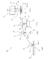
- the die bonder 100 of this embodiment includes a dispenser section 110, a bonding section 120, and guide rails 13 that extend through the sections 110 and 120 and guide the circuit board 14 in the transport direction.
- the circuit board 14 is guided by the guide rail 13 and transferred to the dispenser section 110, and an adhesive is applied to the bonding position 15 of the semiconductor die 40 on the circuit board 14 by the dispenser unit 19.
- the circuit board 14 to which the adhesive has been applied is transported along the guide rails 13 onto the bonding stage 12 of the bonding section 120.
- the circuit board 14 is adsorbed and fixed on the bonding stage 12 and heated by a heater disposed inside the bonding stage 12.
- the bonding section 120 includes a bonding head 10 that operates the collet 20 as a bonding tool, and a pickup that fixes the wafer 60 in a state in which a square semiconductor die 40 that is diced in a grid pattern and is finely cut adheres to the film on the back surface.
- Stage 50 Between the pickup stage 50 and the bonding stage 12, a back camera 30 that images the back surface (lower surface) of the semiconductor die 40 attracted by the collet 20 is disposed.
- the die bonder 100 includes an image processing unit 80 that processes an image acquired by the back camera 30 and a monitor 35 that displays the image.
- the image processing unit 80 is a computer that includes a CPU 81, a storage unit 82, a rear camera interface 87, and a monitor interface 89 that perform information processing and operations such as execution of programs therein.
- the CPU 81, the storage unit 82, the rear camera interface 87, The monitor interface 89 is connected to the data bus 88.
- the rear camera interface 87 is connected to the rear camera 30 by a signal line 91, and the monitor interface 89 is connected to the monitor 35 by a signal line 93.
- Image data acquired by the rear camera 30 is subjected to image processing.
- the unit 80 is configured to be able to display the image on the monitor 35 while being taken in.
- the storage unit 82 stores an image acquisition program 83, an image area definition program 84, a damage detection program 85, and image data 86, which will be described later.
- the die bonder 100 includes a control unit 90 that controls the operation of the dispenser unit 19 of the dispenser section 110 and the operation of the bonding head 10 of the bonding section 120.
- the control unit 90 is a computer including a CPU and a storage unit inside, and is connected to the image processing unit 80, the dispenser section 110, the bonding section 120 and the data bus 92.
- the collet 20 which is a bonding tool attached to the bonding head 10 picks up the semiconductor die 40 on the pickup stage 50. Then, as shown in FIG. 2B, the collet 20 moves the semiconductor die 40 to the position where the longitudinal center line 29 becomes the center of the back camera 30 by the bonding head 10. When the collet 20 moves over the back camera 30, the back camera 30 acquires an image of the lower surface (back surface) of the semiconductor die 40 and inspects the semiconductor die 40 for damage such as cracks as will be described later. To do.
- the collet 20 is moved onto the bonding stage 12 by the bonding head 10 and adsorbed on the collet 20 as shown in FIG. And the bonding position 15 of the semiconductor die 40 on the circuit board 14 are aligned, and the semiconductor die 40 is pressed against the circuit board 14 to perform bonding.
- the collet 20 has a rubber-like collet body 21 provided with an adsorption groove 22 for adsorbing the semiconductor die 40 on the surface thereof, and a disk shape to which the collet body 21 is attached.
- a metal collet holder 23, a shaft 24 extending from the collet holder 23, and a collet shank 25 to which the shaft 24 is fixed are provided.
- the collet shank 25 is attached to the bonding head 10.
- a hole 27 communicating with the suction groove 22 of the collet main body 21 is provided at the center of the collet holder 23 and the shaft 24, and is connected to a vacuum device (not shown).
- the semiconductor die 40 is sucked and fixed to the suction surface 26 which is the lower surface of the collet body 21.
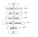
- the control unit 90 shown in FIG. 1 operates the bonding head 10 to move the collet 20 attached to the bonding head 10 to the pickup stage 50 as shown in FIG.
- the model semiconductor die 42 is a semiconductor die 40 of the same type and size as the actual semiconductor die 41 shown in FIG. 6 and subsequent figures that are actually bonded, and has been confirmed in advance to be free from breakage or chipping. It is.
- the model semiconductor die 42 is attracted to the attracting surface 26 of the collet 20, for example, the model semiconductor die 42 is placed on a plate placed on the pickup stage 50, picked up only by suction without being deformed, and picked up. In this case, it is desirable that the model semiconductor die 42 is not damaged.
- step S102 of FIG. 3 when the model semiconductor die 42 is attracted to the collet 20, as shown in FIG. 2B, the collet 20 is moved to the upper side of the rear camera 30, and shown in step S103 of FIG.
- the entire image 70 including the model semiconductor die 42, the collet body 21, and the collet holder 23 is acquired by the rear camera 30.
- the entire image 70 may be an image in the field of view of the rear camera 30 or an image displayed on the monitor 35.
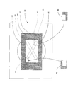
- the rubber collet body 21 is acquired as a black image
- the surface of the model semiconductor 42 and the surface of the collet holder 23, which are metal planes on which light is reflected are acquired as white images. Therefore, as shown in FIG. 5, the operator can easily visually determine the position and area of the model semiconductor die 42 in the entire image 70 from the brightness difference in the entire image 70.
- the operator has the same shape and size as the model semiconductor die 42 in the outline of the model semiconductor die 42 in the entire image 70 displayed on the monitor 35, that is, the model semiconductor die 42.
- Rectile 74 having the same shape as the outer shape of the design dimension (frame line indicated by a one-dot chain line in FIG. 5) is combined to define the area of the model semiconductor die 42 on the screen of the monitor 35 (model semiconductor shown in FIG. 3). Die image area process).
- the operator places square reference image frames 73 at the upper left corner and the lower right corner of the model semiconductor die 42, respectively, and, as shown in step S105 in FIG. Are registered as an upper left reference image 45 and a lower right reference image 46, respectively (reference image registration).
- the upper left reference image 45 has the upper left corner of the model semiconductor die 42 on the lower right side of the image
- the lower right reference image 46 has the lower right corner of the model semiconductor die 42 on the upper left of the image. It has a corner.
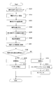
- the die bonder 100 performs bonding of the semiconductor die 40 according to the flowchart shown in FIG.
- the control unit 90 selects one wafer 60 from the wafer 60 that is sucked and fixed onto the pickup stage 50 by the collet 20, as shown in step S201 of FIG.
- the actual semiconductor die 41 is adsorbed and moved to above the rear camera 30 as shown in step S202 of FIG.
- the image processing unit 80 executes the image acquisition program 83 and acquires the entire image 70 as shown in FIG. 6 by the rear camera 30 as shown in step S203 of FIG. 4 (image acquisition process).
- the rubber collet body 21 is acquired as a black image, and the surface of the real semiconductor die 41 and the surface of the collet holder 23, which are metal planes on which light is reflected, are acquired as white images. Is done.
- the image processing unit 80 executes the image region definition program 84, and as shown in step S204 of FIG. 4, the image processing unit 80 determines the brightness of the corners in the upper left reference image 45 acquired previously and the entire image 70. A place where the images in the distribution match is searched by comparing with the distribution. Then, as shown in FIG.
- the position where the boundary line 44 between the upper left collet body 21 of the real semiconductor die 41 and the corner image (brightness distribution) of the upper left reference image 45 is matched in the entire image 70.
- the real semiconductor die 41 is recognized as being located at the upper left corner. Further, a search is made for a location where the corner portion in the lower right reference image 46 acquired earlier and the boundary line 44 in the entire image 70 coincide with each other, and the boundary between the lower right collet body 21 of the real semiconductor die 41 is searched.
- the position where the line 44 and the corner image (lightness distribution) of the lower right reference image 46 match is recognized as the position of the lower right corner of the real semiconductor die 41 in the entire image 70. Then, based on the position of each certified corner, as shown in FIG.
- the position and region (region of the white real semiconductor die 41 shown in FIG. 7) of the actual semiconductor die 41 in the entire image 70 are defined.
- Image region defining step The position of the defined real semiconductor die 41 is defined by the upper left corner and the lower right corner, and the size of the area is defined by the model semiconductor die 42 or the design dimension.
- the image processing unit 80 executes the damage detection program 85, and, as shown in step S206 in FIG. 4 and FIG. 8, the inner portion excluding the periphery of the image region of the defined real semiconductor die 41 is inspected.
- the inspection area 43 is inside the outline of the actual semiconductor die 41, and is an area excluding an area of about 10 pixels from the periphery of the image area of the actual semiconductor die 41, for example.
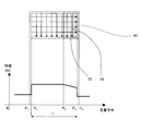
- the image processing unit 80 scans the inspection area 43 shown in FIG. 9, acquires the change in brightness in the scanning direction, and stores it in the storage unit 82. .
- the scanning for example, as shown by an arrow line 75 shown in FIG. 9, along the horizontal direction of the actual semiconductor die 41, brightness is obtained for each pixel or group with one pixel or several pixels as one group. Further, the brightness is obtained by scanning in the longitudinal direction of the actual semiconductor die 41 as indicated by an arrow line 76 shown in FIG.
- the horizontal scanning of the real semiconductor die 41 indicated by the arrow line 75 is performed with the start point P 2 at one end of the inspection region 43 slightly inward from the position P 1 of the end face of the real semiconductor die 41.
- step S208 of FIG. 4 As shown in position P 3 in FIG. 10, or the brightness is rapidly reduced in the scanning direction, as in the case of rapidly and or increased, in the scanning direction of the brightness If the change is large enough to exceed the threshold value, it is determined that there is a crack 48 as shown in step S209 of FIG. 4, and the actual semiconductor die 41 to which the collet 20 is adsorbed has a crack 48. to decide. 4, when the image processing unit 80 outputs a signal to stop the die bonder 100 to the control unit 90, the control unit 90 stops the die bonder 100.
- step S208 in FIG. 11 If the change in brightness is not greater than or equal to the predetermined threshold value in step S208 in FIG. 4, for example, as shown in FIG. 11, even if the actual semiconductor die 41 is slightly lifted from the suction surface 26 of the collet 20, when the lateral direction of the scan of the actual semiconductor die 41 shown by line 75, at a portion such as the brightness toward the position P 4 from the position P 6 of FIG. 11 is changing slowly, it does not determine that there is a crack, the image When there is a gradual change in the lightness of the inside, the die bonder 100 is not stopped because there is damage, and productivity can be improved. When it is determined that the collet attracted to the collet 20 is not damaged, as shown in step S211 in FIG.
- the image processing unit 80 transmits a bonding permission signal to the control unit 90.
- the control unit 90 moves the bonding head 10 and the collet 20 that receive this signal to the position above the bonding stage 12, and the position of the actual semiconductor die 41 and the semiconductor die of the circuit board 14 After matching with the bonding position 15, bonding is performed by pressing the actual semiconductor die 41 onto the circuit board 14 as shown in step S213 of FIG. 4 and FIG. 2C.
- the die bonder 100 of the present embodiment effectively suppresses the bonding of the damaged actual semiconductor die 41 and can improve the quality of the semiconductor device manufactured by the die bonder 100. Play.
- the present invention is not limited to the embodiments described above, and includes all changes and modifications that do not depart from the technical scope or essence of the present invention defined by the claims.
- the present invention can be applied not only to die bonders but also to other types of bonding apparatuses such as flip chip bonders.
Landscapes
- Die Bonding (AREA)
- Testing Or Measuring Of Semiconductors Or The Like (AREA)
- Investigating Materials By The Use Of Optical Means Adapted For Particular Applications (AREA)
Abstract
Description
Claims (4)
- ボンディング装置であって、
半導体ダイを吸着するコレットの吸着面画像とコレットに吸着された半導体ダイの画像とを含む全体画像を撮像するカメラと、
カメラによって取得した各画像を処理する画像処理部と、を備え、
前記画像処理部は、
前記コレットの吸着面画像と半導体ダイの画像との明度差と、前記半導体ダイの基準画像とに基づいて前記全体画像中の前記半導体ダイの画像領域を画定する画像領域画定手段と、
前記画像領域画定手段によって画定した前記半導体ダイの前記画像領域内を走査し、走査方向の明度の変化割合が所定の閾値以上であった場合に、前記半導体ダイの破損であると判断する破損検出手段と、を有するボンディング装置。 - 請求項1に記載のボンディング装置であって、
前記破損検出手段は、前記画像画定手段によって画定した前記半導体ダイの画像領域の内側に検査領域を設定し、前記検査領域内を走査するボンディング装置。 - ボンディング装置による半導体ダイの破損検出方法であって、
半導体ダイを吸着するコレットの吸着面画像とコレットに吸着された前記半導体ダイの画像とを含む全体画像を撮像する画像取得工程と、
前記コレットの吸着面画像と半導体ダイの画像との明度差と、前記半導体ダイの基準画像とに基づいて前記全体画像中の前記半導体ダイの画像領域を画定する画像領域画定工程と、
前記画像画定工程によって画定した前記画像領域内を走査し、走査方向の明度の変化割合が所定の閾値以上であった場合に、半導体ダイの破損であると判断する半導体ダイの破損検出工程と、
を有するボンディング装置による半導体ダイの破損検出方法。 - 請求項3に記載のボンディング装置による半導体ダイの破損検出方法であって、
前記破損検出工程は、前記画像画定工程によって画定した前記半導体ダイの画像領域の内側に検査領域を設定し、前記検査領域内を走査するボンディング装置による半導体ダイの破損検出方法。
Priority Applications (2)
| Application Number | Priority Date | Filing Date | Title |
|---|---|---|---|
| KR1020147033124A KR101732467B1 (ko) | 2013-01-23 | 2013-08-19 | 본딩 장치 및 본딩 장치에 의한 반도체 다이의 파손 검출 방법 |
| CN201380023188.5A CN104937702B (zh) | 2013-01-23 | 2013-08-19 | 粘晶装置以及利用粘晶装置的半导体晶粒的破损检测方法 |
Applications Claiming Priority (2)
| Application Number | Priority Date | Filing Date | Title |
|---|---|---|---|
| JP2013-009877 | 2013-01-23 | ||
| JP2013009877A JP2016076505A (ja) | 2013-01-23 | 2013-01-23 | ダイボンダおよびダイボンダによる半導体ダイの破損検出方法 |
Publications (1)
| Publication Number | Publication Date |
|---|---|
| WO2014115359A1 true WO2014115359A1 (ja) | 2014-07-31 |
Family
ID=51227168
Family Applications (1)
| Application Number | Title | Priority Date | Filing Date |
|---|---|---|---|
| PCT/JP2013/072091 Ceased WO2014115359A1 (ja) | 2013-01-23 | 2013-08-19 | ボンディング装置およびボンディング装置による半導体ダイの破損検出方法 |
Country Status (5)
| Country | Link |
|---|---|
| JP (1) | JP2016076505A (ja) |
| KR (1) | KR101732467B1 (ja) |
| CN (1) | CN104937702B (ja) |
| TW (1) | TWI512854B (ja) |
| WO (1) | WO2014115359A1 (ja) |
Families Citing this family (6)
| Publication number | Priority date | Publication date | Assignee | Title |
|---|---|---|---|---|
| KR102247600B1 (ko) * | 2015-03-16 | 2021-05-03 | 한화정밀기계 주식회사 | 본딩 장치 및 본딩 방법 |
| JP6975551B2 (ja) * | 2017-05-18 | 2021-12-01 | ファスフォードテクノロジ株式会社 | 半導体製造装置および半導体装置の製造方法 |
| JP6839143B2 (ja) * | 2017-09-28 | 2021-03-03 | 芝浦メカトロニクス株式会社 | 素子実装装置、素子実装方法及び素子実装基板製造方法 |
| JP6940207B2 (ja) * | 2018-11-01 | 2021-09-22 | 株式会社新川 | 電子部品実装装置 |
| JP7635075B2 (ja) * | 2021-05-28 | 2025-02-25 | ファスフォードテクノロジ株式会社 | ダイボンディング装置および半導体装置の製造方法 |
| CN120898282A (zh) * | 2023-03-17 | 2025-11-04 | 雅马哈智能机器株式会社 | 芯片保持具、芯片保持装置和半导体装置的制造装置 |
Citations (3)
| Publication number | Priority date | Publication date | Assignee | Title |
|---|---|---|---|---|
| JPS6216538A (ja) * | 1985-07-16 | 1987-01-24 | Toshiba Corp | パタ−ン認識装置 |
| JP2003185590A (ja) * | 2001-12-18 | 2003-07-03 | Stk Technology Co Ltd | ワーク検査方法および装置 |
| JP2007115851A (ja) * | 2005-10-19 | 2007-05-10 | Toshiba Corp | 半導体部品の位置検査方法、位置検査装置および半導体装置の製造方法 |
Family Cites Families (2)
| Publication number | Priority date | Publication date | Assignee | Title |
|---|---|---|---|---|
| CN1518085B (zh) * | 2003-01-15 | 2010-05-12 | 内格夫技术有限公司 | 用于快速在线电光检测晶片缺陷的方法和系统 |
| JP2007278928A (ja) * | 2006-04-10 | 2007-10-25 | Olympus Corp | 欠陥検査装置 |
-
2013
- 2013-01-23 JP JP2013009877A patent/JP2016076505A/ja active Pending
- 2013-08-19 WO PCT/JP2013/072091 patent/WO2014115359A1/ja not_active Ceased
- 2013-08-19 CN CN201380023188.5A patent/CN104937702B/zh active Active
- 2013-08-19 KR KR1020147033124A patent/KR101732467B1/ko active Active
- 2013-09-11 TW TW102132694A patent/TWI512854B/zh active
Patent Citations (3)
| Publication number | Priority date | Publication date | Assignee | Title |
|---|---|---|---|---|
| JPS6216538A (ja) * | 1985-07-16 | 1987-01-24 | Toshiba Corp | パタ−ン認識装置 |
| JP2003185590A (ja) * | 2001-12-18 | 2003-07-03 | Stk Technology Co Ltd | ワーク検査方法および装置 |
| JP2007115851A (ja) * | 2005-10-19 | 2007-05-10 | Toshiba Corp | 半導体部品の位置検査方法、位置検査装置および半導体装置の製造方法 |
Also Published As
| Publication number | Publication date |
|---|---|
| KR20150013613A (ko) | 2015-02-05 |
| TW201430969A (zh) | 2014-08-01 |
| CN104937702A (zh) | 2015-09-23 |
| TWI512854B (zh) | 2015-12-11 |
| KR101732467B1 (ko) | 2017-05-24 |
| JP2016076505A (ja) | 2016-05-12 |
| CN104937702B (zh) | 2017-09-29 |
Similar Documents
| Publication | Publication Date | Title |
|---|---|---|
| TWI671826B (zh) | 黏晶裝置及半導體裝置的製造方法 | |
| CN108364880B (zh) | 半导体制造装置及半导体器件的制造方法 | |
| KR101732467B1 (ko) | 본딩 장치 및 본딩 장치에 의한 반도체 다이의 파손 검출 방법 | |
| JP7225337B2 (ja) | 半導体製造装置および半導体装置の製造方法 | |
| CN101657893B (zh) | 半导体晶圆的异物检测和修复系统及其方法 | |
| TWI638426B (zh) | Stripping device, stripping system, stripping method and information memory medium | |
| CN107078072A (zh) | 位置精度检查方法、位置精度检查装置以及位置检查单元 | |
| CN110729210A (zh) | 半导体制造装置以及半导体器件的制造方法 | |
| CN111725086B (zh) | 半导体制造装置以及半导体器件的制造方法 | |
| JP6110167B2 (ja) | ダイ認識手段及びダイ認識方法並びにダイボンダ | |
| US20240404890A1 (en) | Inspection device, mounting apparatus, inspection method, and non-transitory computer readable recording medium | |
| TWI603077B (zh) | Map matching device, comparison method and comparison program | |
| JP2012199321A (ja) | チップソータおよびチップ移載方法 | |
| JP2019029425A (ja) | ダイボンディング装置、半導体装置の製造方法および半導体製造システム | |
| TWI761582B (zh) | 外觀檢查裝置暨電路基板之製造方法 | |
| JP2014036068A (ja) | ダイボンダおよびボンディングツールの位置検出方法 | |
| KR101124566B1 (ko) | 웨이퍼 검사장치 | |
| CN110024085A (zh) | 镜面裸片图像识别系统 | |
| KR20170036222A (ko) | 다이 검사 방법 | |
| JP2013197278A (ja) | 半導体製造装置 | |
| JP2008226927A (ja) | チップ異常検出方法及びチップ取り出し装置 | |
| CN118782493A (zh) | 半导体装置的制造装置 | |
| CN114361074A (zh) | 晶圆解键合方法 | |
| JP2001076153A (ja) | 円形部品の表面検査方法 |
Legal Events
| Date | Code | Title | Description |
|---|---|---|---|
| 121 | Ep: the epo has been informed by wipo that ep was designated in this application |
Ref document number: 13872889 Country of ref document: EP Kind code of ref document: A1 |
|
| ENP | Entry into the national phase |
Ref document number: 20147033124 Country of ref document: KR Kind code of ref document: A |
|
| NENP | Non-entry into the national phase |
Ref country code: DE |
|
| 122 | Ep: pct application non-entry in european phase |
Ref document number: 13872889 Country of ref document: EP Kind code of ref document: A1 |
|
| NENP | Non-entry into the national phase |
Ref country code: JP |