WO2014111994A1 - 薄型トランス - Google Patents
薄型トランス Download PDFInfo
- Publication number
- WO2014111994A1 WO2014111994A1 PCT/JP2013/006928 JP2013006928W WO2014111994A1 WO 2014111994 A1 WO2014111994 A1 WO 2014111994A1 JP 2013006928 W JP2013006928 W JP 2013006928W WO 2014111994 A1 WO2014111994 A1 WO 2014111994A1
- Authority
- WO
- WIPO (PCT)
- Prior art keywords
- coil
- laminated
- magnetic material
- coil substrate
- pair
- Prior art date
- Legal status (The legal status is an assumption and is not a legal conclusion. Google has not performed a legal analysis and makes no representation as to the accuracy of the status listed.)
- Ceased
Links
Images


Classifications
-
- H—ELECTRICITY
- H01—ELECTRIC ELEMENTS
- H01F—MAGNETS; INDUCTANCES; TRANSFORMERS; SELECTION OF MATERIALS FOR THEIR MAGNETIC PROPERTIES
- H01F27/00—Details of transformers or inductances, in general
- H01F27/28—Coils; Windings; Conductive connections
- H01F27/2804—Printed windings
-
- H—ELECTRICITY
- H01—ELECTRIC ELEMENTS
- H01F—MAGNETS; INDUCTANCES; TRANSFORMERS; SELECTION OF MATERIALS FOR THEIR MAGNETIC PROPERTIES
- H01F27/00—Details of transformers or inductances, in general
- H01F27/28—Coils; Windings; Conductive connections
- H01F27/2804—Printed windings
- H01F2027/2819—Planar transformers with printed windings, e.g. surrounded by two cores and to be mounted on printed circuit
Definitions
- the present invention relates to a thin transformer used for a thin power source of an electronic device.
- FIGS. 3 and 4 as a transformer used for this power source, a plurality of coil substrates 20 on which a primary side coil and a secondary side coil are formed are stacked, and both end portions of the stacked coil substrates 20 are stacked.
- a thin transformer 10 has been proposed in which the laminated portion 20b except 20a is surrounded by a pair of magnetic material cores 30 to form a closed magnetic path, and the pair of magnetic material cores 30 are disposed on a pedestal 40.
- reference numeral 21 denotes a printed layer of the primary side coil and the secondary side coil printed on the coil substrate 20.
- Reference numeral 22 denotes an insulating sheet interposed between the laminated surfaces of the coil substrate 20 and the printed layer 21.
- a symbol t is a terminal inserted through a through hole formed in both end portions 20a of the coil substrate 20 and a hole formed in the base.
- the conventional thin transformer 10 can obtain excellent characteristics by stacking a plurality of coil substrates 20 on which a primary coil and a secondary coil are formed, and can be small and thin. As a result, it is possible to reduce the size and weight of the electronic device and further to save energy.
- the conventional thin transformer 10 has a pair of magnetic material coils 30 directly attached to the coil substrate 20 to form a closed magnetic circuit, a pair of magnetic layers are formed on the upper and lower surfaces of the laminated portion 20b of the laminated coil substrate 20.
- the insulation with the material coil 30 must be ensured, and the primary side coil and the secondary side coil can be formed only on one side of the uppermost layer and the lowermost layer of the laminated coil substrate 20.
- the present invention has been made in view of such circumstances, and when the laminated coil substrate is surrounded by a magnetic material core to form a closed magnetic circuit, the primary coil and the secondary side are not increased without increasing the coil substrate.
- An object of the present invention is to provide a thin transformer capable of adding coils.
- the invention described in claim 1 is characterized in that a plurality of coil substrates each having a primary coil and a secondary coil formed on the front and back surfaces are laminated, and both end portions of the laminated coil substrates.
- the pedestal is an upper surface portion on which the both ends of the laminated coil substrate are supported
- a step portion formed between the upper surface portions and provided with a bottom surface portion on which the magnetic material core is placed, to form an upper surface of the laminated portion of the pair of magnetic material cores and the coil substrate.
- a gap is formed between the lower surface and the lower surface.
- the coil substrate is provided with a plurality of through-holes through which the terminals are inserted at both end portions, and the stepped portion has the above-described portion.
- the stepped portion On the end portion side of the upper surface portion, there is formed a stepped portion including a bottom portion formed to be spaced below the through hole of the coil substrate and a wall portion standing on the upper surface portion from the bottom portion. The terminal extends between the bottom and the coil substrate.
- the laminated portion of the laminated coil substrates is surrounded by the pair of magnetic material cores to form a closed magnetic path, and the magnetic material core is placed on the pedestal.
- the magnetic material core is placed on the pedestal.
- the through-holes are formed after the coil substrates are stacked.
- the terminal is inserted into the hole and the terminal and the coil substrate are connected by soldering, the terminal is extended between the bottom of the stepped portion and the coil substrate, so that the solder is It is easy to pass through the through hole, and the solder wet condition can be confirmed from the outside.
- the terminal flatness can be ensured and the yield can be improved.
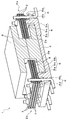
- FIG. 1 is a perspective view of a thin transformer according to an embodiment of the present invention.
- 2 is a cross-sectional view taken along the line II-II in FIG.
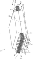
- FIG. 3 is a perspective view of a conventional thin transformer.
- 4 is a cross-sectional view taken along the line IV-IV in FIG.
- the thin transformer 1 and 2 show an embodiment of a thin transformer according to the present invention.
- the thin transformer 1 includes a plurality of coil substrates 2 each having a primary coil and a secondary coil formed on the front and back surfaces.
- the laminated portion 2b excluding both end portions 2a of the laminated coil substrate 2 is surrounded by a pair of magnetic material cores 3 to form a closed magnetic path, and the pair of magnetic material cores 3 are placed on the base 4 It is roughly structured.
- the coil substrate 2 is formed in a rectangular shape in plan view, and a printed layer 7 on which patterns of the primary side coil and the secondary side coil are printed is provided on the front and back surfaces.
- a hole for inserting the convex portion of the magnetic material core 3 is formed in the central portion of the coil substrate 2, and a plurality of through holes into which the terminals t are inserted are provided at both ends 2 a in the longitudinal direction (in the drawing, 9) Drilled.
- substrate 2 is laminated
- the pair of magnetic material cores 3 are E-type ferrite cores.
- the pair of E-type ferrite surrounds the laminated portion 2b of the laminated coil substrate 2 to form a closed letter-shaped magnetic path.
- the pedestal 4 is formed of a synthetic resin and has a rectangular shape in plan view. Further, on the pedestal 4, stepped portions 5 are formed on both ends in the longitudinal direction of the pedestal 4 so as to support both ends 2 a of the laminated coil substrates 2.
- the step portion 5 has an upper surface portion 5 a that supports both end portions 2 a of the coil substrate 2 extending in the short direction of the base 4, and a pair of magnetic material cores 3 are placed between the upper surface portions 5 a.
- a bottom surface portion 5b is formed, and a wall surface portion 5c is formed between the top surface portion 5a and the bottom surface portion 5b.
- a step portion 6 is formed on the end side of each upper surface portion 5a of the step portion 5.
- the step portion 6 has a bottom portion 6a formed to be spaced below the through hole of the coil substrate 2 and extends in the short direction of the pedestal 4, and is erected from the bottom portion 6a to the upper surface portion 5a.
- a wall portion 6b is formed.
- a plurality of hole portions through which the terminal t is inserted are formed in the bottom portion 6 a of the step portion 6 on the same line as the respective through holes formed in the both end portions 2 a of the coil substrate 2.
- the printed layer 7 is formed by printing the patterns of the primary side coil and the secondary side coil on the front and back surfaces of the coil substrate 2.
- a plurality (three in the figure) of the coil substrates 2 on which the printed layers 7 are formed on the front and back surfaces are laminated.
- the insulating sheet 8 is interposed between each lamination surface.
- the laminated portion 2b excluding both end portions 2a of the laminated coil substrate 2 is surrounded by a pair of magnetic material cores 3, and the center convex portion of the magnetic material core 3 is provided in the center of the coil substrate 2. Inserted into the part to form a closed-letter magnetic path.
- the pair of magnetic material cores 3 are placed on the base 4. At that time, both end portions 2a of the laminated coil substrate 2 are respectively supported by the upper surface portion 5a of the step portion 5, and the magnetic material core 3 is placed on the bottom surface portion 5b formed between the upper surface portions 5a. The Thus, a gap is formed between the pair of magnetic material cores 3 and the upper and lower surfaces of the laminated portion 2b of the coil substrate 2.
- the terminals t are inserted through the through holes formed in both end portions 2a of the laminated coil substrate 2 and provided on the bottom portion 6a of the step portion 6 formed on the upper surface portion 5a of the step portion 5.
- the terminal t is inserted through the hole.
- the terminal Solder t in order to connect the terminal t inserted into the through hole of the coil substrate 2 and the primary side coil and the secondary side coil printed on the front and back surfaces of the laminated coil substrate 2, the terminal Solder t.
- the stepped portion 6 formed on the end portion side of the upper surface portion 5a of the stepped portion 5 supporting the both end portions 2a of the laminated coil substrate 2 is interposed between the stepped portion 6 and the coil substrate 2. Since the terminals are extended, it can be confirmed whether the solder has spread over all the coil substrates 2. And the assembly of the thin transformer 1 is completed by soldering all the terminals t.
- the laminated portion 2b of the laminated coil substrate 2 is surrounded by the pair of magnetic material cores 3 to form a closed magnetic path, and the magnetic material core 3 is placed on the pedestal 4.
- both end portions 2a of the laminated coil substrate 2 are respectively supported by the step portions 5, and a gap is formed between the pair of magnetic material cores 3 and the upper and lower surfaces of the laminated portion 2b of the coil substrate 2. Therefore, even if the primary side coil and the secondary side coil are formed on the front and back surfaces of the coil substrate 2, insulation between the magnetic material core 3 and the coil substrate 2 can be ensured. Thereby, a primary side coil and a secondary side coil can be increased, without increasing the coil board
- the terminal t is inserted into the through hole after the coil substrate 2 is laminated.
- the terminal t and the coil substrate 2 are connected by soldering, the terminal t extends between the bottom portion 6a of the stepped portion 6 and the coil substrate 2, so that the solder can easily pass through the through hole. Also, the solder wet condition can be confirmed from the outside. As a result, even if the primary side coil and the secondary side coil are formed on the front and back surfaces of the coil substrate 2, the terminal flatness can be ensured and the yield can be improved.
- the thin transformer 1 according to the present invention is provided with the printed layers 7 on the front and back surfaces of which the primary coil and secondary coil patterns are printed, respectively, on the three coil substrates 2.
- the present invention is not limited to this, and a gap may be secured between the upper surface and the lower surface of the laminated portion 2b of the coil substrate 2 laminated with the pair of magnetic material cores 3. If possible, it is possible to use even more coil substrates 2.
- the pair of magnetic material cores 3 has been described only when an E-type ferrite core is used.
- the present invention is not limited to this, and a combination of E-type and I-type ferrite cores is also possible. .
Landscapes
- Engineering & Computer Science (AREA)
- Power Engineering (AREA)
- Coils Or Transformers For Communication (AREA)
- Coils Of Transformers For General Uses (AREA)
Abstract
積層されたコイル基板を磁性材コアにより囲繞して閉磁路を形成した際に、当該コイル基板を増やすことなく、一次側コイルおよび二次側コイルを増設することが可能な薄型トランスを提供する。本発明の薄型トランスは、表裏面に一次側コイルおよび二次側コイルが形成されたコイル基板(2)が複数積層されるとともに、積層されたコイル基板(2)の両端部(2a)を除く積層部(2b)が一対の磁性材コア(3)により囲繞されて閉磁路が形成され台座(4)上に載置された薄型トランスにおいて、台座(4)は、積層されたコイル基板(2)の両端部(2a)が支持される上面部(5a)と、当該上面部(5a)間に形成されて一対の磁性材コア(3)が載置される底面部(5b)とを備えた段部(5)が形成されることにより、一対の磁性材コア(3)とコイル基板(2)の積層部(2b)の上面および下面との間に間隙が形成されている。
Description
本発明は、電子装置の薄型電源などに用いられる薄型トランスに関するものである。
近年、コンピュータや通信機器などの電子装置、特に携帯型の電子装置の普及は著しい。それに伴って、これら電子装置の小型化および軽量化が目覚ましいスピードで進み、さらにエコロジーや省エネへの意識の高まりから、その進化は一段と加速されてきている。
そのため、さらなる小型化および軽量化の実現に向けて、これら電子装置に用いられる電源においても、小型かつ薄型のものが求められている。この電源の小型かつ薄型に対応させる構成部品の一つとしてトランスがある。このトランスを小型かつ薄型にすることにより、電源自体の小型かつ薄型に繋げることができる。
そこで、この電源に用いられるトランスとして、図3および図4に示すように、一次側コイルおよび二次側コイルが形成されたコイル基板20を複数積層するとともに、積層されたコイル基板20の両端部20aを除く積層部20bを一対の磁性材コア30により囲繞して閉磁路が形成され、かつ一対の磁性材コア30が台座40に配設された薄型トランス10が提案されている。
なお、図3および図4において、符号21は、コイル基板20にプリントされた一次側コイルおよび二次側コイルのプリント層である。また、符号22は、コイル基板20のプリント層21との積層面の間に介装される絶縁シートである。さらに、符号tは、コイル基板20の両端部20aに穿設された貫通孔および台座に穿設された孔部に挿通される端子である。
この従来の薄型トランス10は、一次側コイルおよび二次側コイルが形成されたコイル基板20を複数積層することにより、優れた特性を得ることができるとともに、小型かつ薄型を図ることができる。これにより、電子機器の小型化および軽量化、さらには省エネに対応させることができる。
ところが、上記従来の薄型トランス10は、コイル基板20に直接一対の磁性材コイル30を取り付けて閉磁路を形成するため、積層したコイル基板20の積層部20bの上面と下面とに、一対の磁性材コイル30との絶縁を確保しなければならず、積層されたコイル基板20の最上層と最下層には、一方側の面にしか一次側コイルおよび二次側コイルを形成することができない。
このため、大電流化の対応など性能を向上させる目的により、一次側コイルおよび二次側コイルを増設する場合には、コイル基板20の枚数を増やす必要があり、製造コストが嵩むとともに、薄型化に対応しづらいという問題がある。
本発明は、かかる事情に鑑みてなされたもので、積層されたコイル基板を磁性材コアにより囲繞して閉磁路を形成した際に、当該コイル基板を増やすことなく、一次側コイルおよび二次側コイルを増設することが可能な薄型トランスを提供することを課題とするものである。
上記課題を解決するために、請求項1に記載の発明は、表裏面に一次側コイルおよび二次側コイルが形成されたコイル基板が複数積層されるとともに、積層された上記コイル基板の両端部を除く積層部が一対の磁性材コアにより囲繞されて閉磁路が形成され台座上に載置された薄型トランスにおいて、上記台座は、積層された上記コイル基板の上記両端部が支持される上面部と、当該上面部間に形成されて上記磁性材コアが載置される底面部とを備えた段部が形成されることにより、上記一対の磁性材コアと当該コイル基板の上記積層部の上面および下面との間に間隙が形成されていることを特徴とするものである。
また、請求項2に記載の発明は、請求項1に記載の発明において、上記コイル基板には、上記両端部に端子を挿通する複数の貫通孔が穿設されるとともに、上記段部の上記上面部の端部側には、上記コイル基板の上記貫通孔の下方に離間して形成される底部と、当該底部から上記上面部に立設される壁部を備えた段差部が形成されていることにより、当該底部と上記コイル基板との間に上記端子が延出されることを特徴とするものである。
請求項1~2に記載の本発明によれば、積層されたコイル基板の積層部を一対の磁性材コアにより囲繞して閉磁路を形成して、当該磁性材コアを台座上に載置する際に、積層された上記コイル基板の両端部を段部により各々支持して、上記一対の磁性材コアと上記コイル基板の上記積層部の上面および下面との間に間隙を形成するため、上記コイル基板の表裏面に1次側コイルおよび2次側コイルを形成しても、上記磁性材コアと当該コイル基板との絶縁を確保することができる。これにより、上記コイル基板を増やすことなく、1次側コイルおよび2次側コイルを増やすことができ、製造コストを抑えることができる。
請求項2に記載の発明によれば、上記コイル基板の上記両端部に端子を挿通する複数の貫通孔の下方に、段差部が形成されているため、上記コイル基板を積層した後に、上記貫通孔に上記端子を挿通して、当該端子と上記コイル基板とをハンダ付けにより結線する際に、上記段差部の底部と上記コイル基板との間に上記端子が延出されることにより、ハンダが上記貫通孔を通り易く、またハンダ濡れ状況を外部から確認することができる。この結果、上記コイル基板の表裏面に1次側コイルおよび2次側コイルを形成しても、端子平面度を確保することができ、歩留まりを向上させることができる。
図1および図2は、本発明に係る薄型トランスの一実施形態を示すもので、この薄型トランス1は、表裏面に一次側コイルおよび二次側コイルが形成されたコイル基板2が複数積層されるとともに、積層されたコイル基板2の両端部2aを除く積層部2bが一対の磁性材コア3により囲繞されて閉磁路が形成され、かつ一対の磁性材コア3が台座4に載置されて概略構成されている。
ここで、コイル基板2は、平面視において長方形に形成されているとともに、表裏面には、1次側コイルおよび2次側コイルのパターンがプリントされたプリント層7が設けられている。また、コイル基板2の中央部に磁性材コア3の凸部が挿入される孔部が形成されているとともに、長手方向の両端部2aに、端子tが挿入される貫通孔が複数(図では9つ)穿設されている。そして、コイル基板2は、複数枚(図では3枚)が積層され、積層面には絶縁シート8が介装されている。
そして、一対の磁性材コア3は、E型のフェライトコアが用いられている。この一対のE型のフェライトが、積層されたコイル基板2の積層部2bを囲繞して日字状の閉磁路が形成されている。
さらに、台座4は、合成樹脂により形成されるとともに、平面視において長方形に形成されている。また、台座4には、当該台座4の長手方向の両端部側に、積層されたコイル基板2の両端部2aが支持される段部5が形成されている。この段部5は、コイル基板2の両端部2aを支持する上面部5aが台座4の短手方向に延設されているとともに、この上面部5a間に一対の磁性材コア3が載置される底面部5bが形成され、かつ上面部5aと底面部5bとの間に壁面部5cが各々形成されている。
また、段部5の各々の上面部5aの端部側には、段差部6が形成されている。この段差部6は、コイル基板2の上記貫通孔の下方に離間して形成された底部6aが、台座4の短手方向に延設されているとともに、底部6aから上面部5aに立設される壁部6bが形成されている。
さらに、段差部6の底部6aには、コイル基板2の両端部2aに穿設された各々の上記
貫通孔と同軸線上に、端子tが挿通される孔部が複数穿設されている。
貫通孔と同軸線上に、端子tが挿通される孔部が複数穿設されている。
上記構成からなる薄型トランス1を組み立てる際には、まず、コイル基板2の表裏面に一次側コイルおよび2次側コイルのパターンをプリントしてプリント層7を形成する。次いで、これらプリント層7が表裏面に形成されたコイル基板2を複数(図では3枚)積層する。その際に、各々の積層面の間に絶縁シート8を介装させる。
そして、積層されたコイル基板2の両端部2aを除く積層部2bを一対の磁性材コア3によって囲繞するとともに、当該磁性材コア3の中央の凸部をコイル基板2の中央に設けられた孔部に挿入して、日字状の閉磁路を形成する。
次に、台座4上に一対の磁性材コア3を載置する。その際に、積層されたコイル基板2の両端部2aが段部5の上面部5aにより各々支持されるとともに、当該磁性材コア3が上面部5a間に形成された底面部5bに載置される。これにより、一対の磁性材コア3とコイル基板2の積層部2bの上面および下面との間に間隙が形成される。
そして、積層されたコイル基板2の両端部2aに各々穿設された上記貫通孔に、端子tを挿通させるとともに、段部5の上面部5aに形成された段差部6の底部6aに設けられた孔部に、端子tを挿通させる。
さらに、コイル基板2の上記貫通孔に挿通された端子tと、積層された当該コイル基板2の各々の表裏面にプリントされた1次側コイルおよび2次側コイルとを結線するために、端子tをハンダ付けする。その際に、積層されたコイル基板2の両端部2aを支持している段部5の上面部5aの端部側に形成された段差部6により、当該段差部6とコイル基板2との間に上記端子が延出されているため、ハンダが全てのコイル基板2に行き渡ったかを確認することができる。
そして、全ての端子tをハンダ付けすることにより、薄型トランス1の組み立てが完了する。
そして、全ての端子tをハンダ付けすることにより、薄型トランス1の組み立てが完了する。
以上の構成からなる薄型トランス1によれば、積層されたコイル基板2の積層部2bを一対の磁性材コア3により囲繞して閉磁路を形成して、磁性材コア3を台座4に載置する際に、積層されたコイル基板2の両端部2aを段部5により各々支持して、一対の磁性材コア3とコイル基板2の積層部2bの上面および下面との間に間隙を形成するため、コイル基板2の表裏面に1次側コイルおよび2次側コイルを形成しても、磁性材コア3とコイル基板2との絶縁を確保することができる。これにより、コイル基板2を増やすことなく、1次側コイルおよび2次側コイルを増やすことができ、製造コストを抑えることができる。
また、コイル基板2の両端部2aに端子tを挿通する複数の上記貫通孔の下方に、段差部6が形成されているため、コイル基板2を積層した後に、上記貫通孔に端子tを挿通して、端子tとコイル基板2とをハンダ付けにより結線する際に、段差部6の底部6aとコイル基板2との間に端子tが延出されることにより、ハンダが上記貫通孔を通り易く、またハンダ濡れ状況を外部から確認することができる。この結果、コイル基板2の表裏面に1次側コイルおよび2次側コイルを形成しても、端子平面度を確保することができ、歩留まりを向上させることができる。
なお、上記実施形態においては、本発明に係る薄型トランス1が、表裏面に1次側コイルおよび2次側コイルのパターンをプリントしたプリント層7が、三枚のコイル基板2に各々設けられた場合についてのみ説明したが、本発明はこれに限定されるものではなく、一対の磁性材コア3と積層されたコイル基板2の積層部2bの上面と下面との間に間隙が確保することができれば、より多くのコイル基板2を用いても対応可能である。
また、一対の磁性材コア3をE型のフェライトコアを用いる場合のみ説明したが、本発明はこれに限定されるものではなく、E型とI型のフェライトコアを組み合わせても対応可能である。
電子機器などの薄型電源に利用することができる。
1 薄型トランス
2 コイル基板
3 一対の磁性材コア
4 台座
5 段部
5a 上面部
5b 底面部
5c 壁面部
6 段差部
6a 底部
6b 壁部
7 プリント層
8 絶縁シート
t 端子
2 コイル基板
3 一対の磁性材コア
4 台座
5 段部
5a 上面部
5b 底面部
5c 壁面部
6 段差部
6a 底部
6b 壁部
7 プリント層
8 絶縁シート
t 端子
Claims (2)
- 表裏面に一次側コイルおよび二次側コイルが形成されたコイル基板が複数積層されるとともに、積層された上記コイル基板の両端部を除く積層部が一対の磁性材コアにより囲繞されて閉磁路が形成され台座上に載置された薄型トランスにおいて、
上記台座は、積層された上記コイル基板の上記両端部が支持される上面部と、当該上面部間に形成されて上記一対の磁性材コアが載置される底面部とを備えた段部が形成されることにより、上記一対の磁性材コアと当該コイル基板の上記積層部の上面および下面との間に間隙が形成されていることを特徴とする薄型トランス。 - 上記コイル基板には、上記両端部に端子を挿通する複数の貫通孔が穿設されるとともに、
上記段部の上記上面部の端部側には、上記コイル基板の上記貫通孔の下方に離間して形成される底部と、当該底部から上記上面部に立設される壁部を備えた段差部が形成されていることにより、当該底部と上記コイル基板との間に上記端子が延出されることを特徴とする請求項1に記載の薄型トランス。
Priority Applications (1)
| Application Number | Priority Date | Filing Date | Title |
|---|---|---|---|
| RU2015122107A RU2015122107A (ru) | 2013-01-17 | 2013-11-26 | Тонкий трансформатор |
Applications Claiming Priority (2)
| Application Number | Priority Date | Filing Date | Title |
|---|---|---|---|
| JP2013006441A JP6194506B2 (ja) | 2013-01-17 | 2013-01-17 | 薄型トランス |
| JP2013-006441 | 2013-01-17 |
Publications (2)
| Publication Number | Publication Date |
|---|---|
| WO2014111994A1 true WO2014111994A1 (ja) | 2014-07-24 |
| WO2014111994A8 WO2014111994A8 (ja) | 2015-05-14 |
Family
ID=51209123
Family Applications (1)
| Application Number | Title | Priority Date | Filing Date |
|---|---|---|---|
| PCT/JP2013/006928 Ceased WO2014111994A1 (ja) | 2013-01-17 | 2013-11-26 | 薄型トランス |
Country Status (3)
| Country | Link |
|---|---|
| JP (1) | JP6194506B2 (ja) |
| RU (1) | RU2015122107A (ja) |
| WO (1) | WO2014111994A1 (ja) |
Cited By (1)
| Publication number | Priority date | Publication date | Assignee | Title |
|---|---|---|---|---|
| US10178787B2 (en) | 2014-09-19 | 2019-01-08 | Murata Manufacturing Co., Ltd. | Header for mounting a planar transformer on a motherboard |
Families Citing this family (1)
| Publication number | Priority date | Publication date | Assignee | Title |
|---|---|---|---|---|
| WO2025183028A1 (ja) * | 2024-02-27 | 2025-09-04 | 国立大学法人東北大学 | トランス及びコンバータ |
Citations (3)
| Publication number | Priority date | Publication date | Assignee | Title |
|---|---|---|---|---|
| JP2008166625A (ja) * | 2006-12-29 | 2008-07-17 | Matsushita Electric Works Ltd | 基板トランス |
| WO2011027792A1 (ja) * | 2009-09-01 | 2011-03-10 | 株式会社ティーアイビーシー | 回路基板の製造方法および回路基板 |
| JP2012156461A (ja) * | 2011-01-28 | 2012-08-16 | Toyota Industries Corp | 電子機器 |
Family Cites Families (2)
| Publication number | Priority date | Publication date | Assignee | Title |
|---|---|---|---|---|
| JPH0869935A (ja) * | 1994-06-21 | 1996-03-12 | Sumitomo Special Metals Co Ltd | 多層プリントコイル基板の作製方法並びにプリントコイル基板及び多層プリントコイル基板 |
| JPH09213525A (ja) * | 1996-02-01 | 1997-08-15 | Murata Mfg Co Ltd | 積層シ−トコイル装置 |
-
2013
- 2013-01-17 JP JP2013006441A patent/JP6194506B2/ja not_active Expired - Fee Related
- 2013-11-26 RU RU2015122107A patent/RU2015122107A/ru not_active Application Discontinuation
- 2013-11-26 WO PCT/JP2013/006928 patent/WO2014111994A1/ja not_active Ceased
Patent Citations (3)
| Publication number | Priority date | Publication date | Assignee | Title |
|---|---|---|---|---|
| JP2008166625A (ja) * | 2006-12-29 | 2008-07-17 | Matsushita Electric Works Ltd | 基板トランス |
| WO2011027792A1 (ja) * | 2009-09-01 | 2011-03-10 | 株式会社ティーアイビーシー | 回路基板の製造方法および回路基板 |
| JP2012156461A (ja) * | 2011-01-28 | 2012-08-16 | Toyota Industries Corp | 電子機器 |
Cited By (2)
| Publication number | Priority date | Publication date | Assignee | Title |
|---|---|---|---|---|
| US10178787B2 (en) | 2014-09-19 | 2019-01-08 | Murata Manufacturing Co., Ltd. | Header for mounting a planar transformer on a motherboard |
| GB2530321B (en) * | 2014-09-19 | 2019-04-17 | Murata Manufacturing Co | Electronic device |
Also Published As
| Publication number | Publication date |
|---|---|
| JP2014138109A (ja) | 2014-07-28 |
| WO2014111994A8 (ja) | 2015-05-14 |
| JP6194506B2 (ja) | 2017-09-13 |
| RU2015122107A (ru) | 2017-01-10 |
Similar Documents
| Publication | Publication Date | Title |
|---|---|---|
| KR101133397B1 (ko) | 평면형 트랜스포머 및 이의 제조 방법 | |
| US10141107B2 (en) | Miniature planar transformer | |
| KR101121645B1 (ko) | 평면형 트랜스포머 | |
| US9424979B2 (en) | Magnetic element with multiple air gaps | |
| JP2011530172A5 (ja) | ||
| CN103269149B (zh) | 适用于正激同步整流的pcb平板磁性器件 | |
| KR20110024431A (ko) | 평면형 트랜스포머 | |
| JP6116806B2 (ja) | 薄型コアコイルおよび薄型トランス | |
| JPWO2012137386A1 (ja) | 積層型インダクタ素子およびその製造方法 | |
| US8188825B2 (en) | Transformer structure | |
| JP2010165973A (ja) | 積層インダクタ | |
| CN102881405B (zh) | 变压器与电感元件的组合结构及其形成方法 | |
| JP5998611B2 (ja) | コイルユニット、基板ユニット、及び電源装置 | |
| JP6194506B2 (ja) | 薄型トランス | |
| CN201663036U (zh) | 磁性元件 | |
| JP2013115053A (ja) | ノイズ対策電子部品の回路基板への実装構造 | |
| CN202796397U (zh) | 一种pcb平面变压器 | |
| TWI437584B (zh) | 變壓器與電感元件之組合結構及其形成方法 | |
| JP5311462B2 (ja) | 多層基板トランス | |
| CN103906378B (zh) | 承载大电流的电路板的制作方法及承载大电流的电路板 | |
| CN205160916U (zh) | 一种pcb平面变压器及其pcb板 | |
| TWM467156U (zh) | 印製電路板組及平面變壓器 | |
| CN107171058B (zh) | 天线模块 | |
| JPWO2013171923A1 (ja) | インダクタ素子 | |
| JP2013207151A (ja) | トランス |
Legal Events
| Date | Code | Title | Description |
|---|---|---|---|
| 121 | Ep: the epo has been informed by wipo that ep was designated in this application |
Ref document number: 13871381 Country of ref document: EP Kind code of ref document: A1 |
|
| ENP | Entry into the national phase |
Ref document number: 2015122107 Country of ref document: RU Kind code of ref document: A |
|
| NENP | Non-entry into the national phase |
Ref country code: DE |
|
| 122 | Ep: pct application non-entry in european phase |
Ref document number: 13871381 Country of ref document: EP Kind code of ref document: A1 |