WO2014104552A1 - 저마늄을 이용한 반도체 소자의 접합 영역에서의 결함 치유 방법 - Google Patents
저마늄을 이용한 반도체 소자의 접합 영역에서의 결함 치유 방법 Download PDFInfo
- Publication number
- WO2014104552A1 WO2014104552A1 PCT/KR2013/009502 KR2013009502W WO2014104552A1 WO 2014104552 A1 WO2014104552 A1 WO 2014104552A1 KR 2013009502 W KR2013009502 W KR 2013009502W WO 2014104552 A1 WO2014104552 A1 WO 2014104552A1
- Authority
- WO
- WIPO (PCT)
- Prior art keywords
- layer
- forming
- heat treatment
- region
- electrode
- Prior art date
- Legal status (The legal status is an assumption and is not a legal conclusion. Google has not performed a legal analysis and makes no representation as to the accuracy of the status listed.)
- Ceased
Links
Images


Classifications
-
- H—ELECTRICITY
- H10—SEMICONDUCTOR DEVICES; ELECTRIC SOLID-STATE DEVICES NOT OTHERWISE PROVIDED FOR
- H10P—GENERIC PROCESSES OR APPARATUS FOR THE MANUFACTURE OR TREATMENT OF DEVICES COVERED BY CLASS H10
- H10P36/00—Gettering within semiconductor bodies
- H10P36/03—Gettering within semiconductor bodies within silicon bodies
-
- H—ELECTRICITY
- H10—SEMICONDUCTOR DEVICES; ELECTRIC SOLID-STATE DEVICES NOT OTHERWISE PROVIDED FOR
- H10P—GENERIC PROCESSES OR APPARATUS FOR THE MANUFACTURE OR TREATMENT OF DEVICES COVERED BY CLASS H10
- H10P30/00—Ion implantation into wafers, substrates or parts of devices
- H10P30/20—Ion implantation into wafers, substrates or parts of devices into semiconductor materials, e.g. for doping
- H10P30/202—Ion implantation into wafers, substrates or parts of devices into semiconductor materials, e.g. for doping characterised by the semiconductor materials
- H10P30/204—Ion implantation into wafers, substrates or parts of devices into semiconductor materials, e.g. for doping characterised by the semiconductor materials into Group IV semiconductors
-
- H—ELECTRICITY
- H10—SEMICONDUCTOR DEVICES; ELECTRIC SOLID-STATE DEVICES NOT OTHERWISE PROVIDED FOR
- H10D—INORGANIC ELECTRIC SEMICONDUCTOR DEVICES
- H10D64/00—Electrodes of devices having potential barriers
- H10D64/01—Manufacture or treatment
- H10D64/011—Manufacture or treatment of electrodes ohmically coupled to a semiconductor
- H10D64/0111—Manufacture or treatment of electrodes ohmically coupled to a semiconductor to Group IV semiconductors
-
- H—ELECTRICITY
- H10—SEMICONDUCTOR DEVICES; ELECTRIC SOLID-STATE DEVICES NOT OTHERWISE PROVIDED FOR
- H10D—INORGANIC ELECTRIC SEMICONDUCTOR DEVICES
- H10D64/00—Electrodes of devices having potential barriers
- H10D64/01—Manufacture or treatment
- H10D64/011—Manufacture or treatment of electrodes ohmically coupled to a semiconductor
- H10D64/0111—Manufacture or treatment of electrodes ohmically coupled to a semiconductor to Group IV semiconductors
- H10D64/0112—Manufacture or treatment of electrodes ohmically coupled to a semiconductor to Group IV semiconductors using conductive layers comprising silicides
-
- H—ELECTRICITY
- H10—SEMICONDUCTOR DEVICES; ELECTRIC SOLID-STATE DEVICES NOT OTHERWISE PROVIDED FOR
- H10D—INORGANIC ELECTRIC SEMICONDUCTOR DEVICES
- H10D64/00—Electrodes of devices having potential barriers
- H10D64/60—Electrodes characterised by their materials
- H10D64/62—Electrodes ohmically coupled to a semiconductor
-
- H—ELECTRICITY
- H10—SEMICONDUCTOR DEVICES; ELECTRIC SOLID-STATE DEVICES NOT OTHERWISE PROVIDED FOR
- H10P—GENERIC PROCESSES OR APPARATUS FOR THE MANUFACTURE OR TREATMENT OF DEVICES COVERED BY CLASS H10
- H10P30/00—Ion implantation into wafers, substrates or parts of devices
- H10P30/20—Ion implantation into wafers, substrates or parts of devices into semiconductor materials, e.g. for doping
- H10P30/21—Ion implantation into wafers, substrates or parts of devices into semiconductor materials, e.g. for doping of electrically active species
-
- H—ELECTRICITY
- H10—SEMICONDUCTOR DEVICES; ELECTRIC SOLID-STATE DEVICES NOT OTHERWISE PROVIDED FOR
- H10P—GENERIC PROCESSES OR APPARATUS FOR THE MANUFACTURE OR TREATMENT OF DEVICES COVERED BY CLASS H10
- H10P30/00—Ion implantation into wafers, substrates or parts of devices
- H10P30/20—Ion implantation into wafers, substrates or parts of devices into semiconductor materials, e.g. for doping
- H10P30/28—Ion implantation into wafers, substrates or parts of devices into semiconductor materials, e.g. for doping characterised by an annealing step, e.g. for activation of dopants
-
- H—ELECTRICITY
- H10—SEMICONDUCTOR DEVICES; ELECTRIC SOLID-STATE DEVICES NOT OTHERWISE PROVIDED FOR
- H10P—GENERIC PROCESSES OR APPARATUS FOR THE MANUFACTURE OR TREATMENT OF DEVICES COVERED BY CLASS H10
- H10P34/00—Irradiation with electromagnetic or particle radiation of wafers, substrates or parts of devices
-
- H—ELECTRICITY
- H10—SEMICONDUCTOR DEVICES; ELECTRIC SOLID-STATE DEVICES NOT OTHERWISE PROVIDED FOR
- H10P—GENERIC PROCESSES OR APPARATUS FOR THE MANUFACTURE OR TREATMENT OF DEVICES COVERED BY CLASS H10
- H10P95/00—Generic processes or apparatus for manufacture or treatments not covered by the other groups of this subclass
- H10P95/90—Thermal treatments, e.g. annealing or sintering
Definitions
- the present invention relates to a method for healing a defect in a junction region in a semiconductor device, wherein a defect in a junction is performed by performing heat treatment for 1 to 3 hours at 600 ° C to 700 ° C after the formation of the n + Ge region.
- the present invention relates to a method for healing defects in a junction region of a semiconductor device using germanium to heal the defects.
- the drain current is controlled by changing the channel region according to the magnitude of the voltage applied to the gate.
- the p-type well and the n-type source are controlled.
- an oxide film or a photoresist is defined by a photolithography process to form an n-type drain region, and then a method of determining an implantation depth, an implantation concentration, or the like through energy of a dopant to be implanted.
- a semiconductor such as a field effect transistor forms conductive regions having different conductivity types, such as p-type or n-type, on a silicon substrate. These conductive regions are essentially a junction, hereinafter, to clarify meaning. And minimizing defects in the junction part during fabrication of the semiconductor device have been studied as a way to solve the defects of the miniaturized semiconductor device.
- the defect healing in the junction of the semiconductor device plays a very important role for improving the characteristics due to the high integration and miniaturization of the semiconductor device.
- the prior art includes technologies such as a method of manufacturing a semiconductor device registered in Korea Patent Office No. 10-0403992, a method of manufacturing a MOS transistor, and the like.
- the technique proposed for the defect healing is vaguely described as a heat treatment at a high temperature without specifying the temperature region or the like, and still does not provide a reliable method for healing the defect.
- the present invention is to solve the above problems, in the junction region of the semiconductor device using germanium to heal a defect in the junction by performing heat treatment for 1 to 3 hours at 600 °C ⁇ 700 °C after n + Ge region formation It is aimed at providing the method of healing defects.
- another object of the present invention is to provide a method for healing defects in a junction region of a semiconductor device using germanium to minimize leakage current by forming a germanide through heat treatment after electrode formation in order to reduce the junction depth.
- the present invention provides a first step of growing a p-Ge layer on a substrate, a second step of patterning an n + Ge region by depositing an oxide film on the p-Ge layer, and a third step of forming an n + Ge region by ion implantation with a p-type dopant in a pattern for forming an n + Ge region, and a fourth capping oxide layer formed on the p-Ge layer after the n + Ge region is formed And a fifth step of performing heat treatment for 1 hour to 3 hours at 600 ° C. to 700 ° C. after forming the capping oxide film, and patterning the capping oxide film for electrode formation after the heat treatment, and depositing an electrode.
- the technical gist of the defect healing method in the junction region of the semiconductor device using germanium is characterized by comprising a sixth step.
- the present invention also provides a first step of growing a p-Ge layer on a substrate, and a second step of forming an n + Ge layer using in-situ doping of a p-type dopant on the p-Ge layer. And a third step of forming an n + Ge region by etching after patterning to form an n + Ge region, and a fourth step of forming a capping oxide layer on the p-Ge layer after forming the n + Ge region; A fifth step of performing heat treatment for 1 hour to 3 hours at 600 ° C. to 700 ° C. after forming the capping oxide film, and patterning the capping oxide film for electrode formation after the heat treatment, and depositing an electrode It is another technical gist of a method for healing defects in a junction region of a semiconductor device using germanium.
- the present invention also provides a first step of growing a p-Ge layer on a substrate, and depositing an oxide film on the p-Ge layer to form an n + Ge region, and patterning the oxide film or the oxide film and the p-Ge layer. Etching a second step, and forming a n + Ge layer using an in-situ doping of a p-type dopant on the p-Ge layer for forming the n + Ge region, and the n + Ge A fourth step of forming a capping oxide film on the oxide layer after the layer is formed, a fifth step of performing a heat treatment at 600 ° C. to 700 ° C.
- Another technical gist of the method is to fix a defect in a junction region of a germanium semiconductor using germanium, comprising the step of patterning the capping oxide film for electrode formation and depositing an electrode.
- the p-Ge layer of the first step after growing Ge 300 ⁇ 500nm at 350 ⁇ 450 °C, 7.5 ⁇ 8.5Pa on a silicon (Si) substrate 20 minutes ⁇ 1 hour H 2 atmosphere at 800 ⁇ 150 °C It is more preferable that the heat treatment is carried out at, and the Ge layer is further grown at 550-650 ° C. and 7.5-8.5 Pa after repeating the above process once more.
- the electrode of the sixth step it is preferable to use any one of Ti, Ni, Pd, Pt, Ta, Cu, W, Co, Zr, Cr, Mn and Mo, in order to reduce the heat treatment deepened
- defects are generated during the junction formation of the semiconductor device, but the Ge defects in the n + / p junction can be healed through the heat treatment process, and the junction deepened through the heat treatment can be relatively reduced, thereby minimizing the leakage current. There is an effect that is more useful in improving the characteristics of the device, and realizing high integration and miniaturization of the semiconductor device.
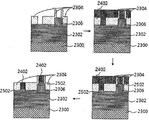
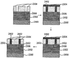
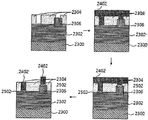
- FIG. 4 shows a schematic diagram of an electrode forming method according to the above process.
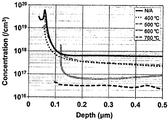
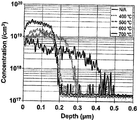
- 5-ECV analysis results according to the heat treatment temperature after Ge ion implantation on the p-Ge layer and intentional generation of point defects.
- the present invention relates to a method for healing defects in a junction region in a semiconductor device, wherein heat treatment is performed at 600 ° C. to 700 ° C. for 1 to 3 hours after heat treatment, in particular, to form a n + Ge region. It is for.
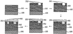
- FIG. 1 1, 2, and 3 are schematic views of three processes according to the present invention
- FIG. 4 is a schematic diagram of an electrode forming method according to the above processes.
- the present invention is largely implemented by three processes.
- the process 1 process is illustrated in FIGS. 1 and 4A, and a first step of growing the p-Ge layer 102 on the substrate 100, and an oxide film on the upper layer of the p-Ge layer 102.
- the substrate 100 uses silicon (Si) or silicon germanium (SiGe).
- the p-Ge layer 102 is grown on the substrate, which is particularly doped with an n-type dopant when the Ge layer is grown or has a p-Ge property only with the Ge layer itself (intrinsic Ge, i-Ge).
- This p-Ge layer growth does not limit a particular deposition method, but is formed by known physical and chemical vacuum deposition methods.
- the p-Ge layer of the first step is grown on the silicon (Si) substrate at 350 ° C. to 450 ° C. and 7.5 Pa to 8.5 Pa at 300 to 500 nm, and then at 20 ° C. to 800 ° C. to 850 ° C.
- Heat treatment is performed in H 2 atmosphere for 1 minute to 1 hour, and the above process is repeated one more time, followed by further growth of the Ge layer at 550 ° C to 650 ° C and 7.5Pa to 8.5Pa, followed by 700 ° C to 800 ° C. It is preferable to form by performing a heat treatment in the H 2 atmosphere for 10 minutes to 20 minutes at, to minimize the defects in the interface between the silicon substrate and the p-Ge layer or inside the p-Ge layer.
- an oxide film 202 is deposited on the p-Ge layer 102, and patterning is performed to form an n + Ge region 302.
- SiO 2 is mainly used as the oxide film 202, and a patterning method is to select an etching gas which is widely used, and then etching using a reactive ion etcher (RIE) or another known method such as photolithography. use.
- RIE reactive ion etcher
- the n + Ge region 302 is formed on the pattern for forming the n + Ge region 302 by p-type dopants such as P, As, and Sb through an ion implantation method, and then dopant loss and out are performed during the heat treatment process.
- a capping oxide film 402 is formed to prevent out-diffudion.
- heat treatment is performed at 600 ° C. to 700 ° C. for 1 hour to 3 hours. That is, the n + Ge region formed through ion implantation is activated, and heat treatment is performed in an N 2 atmosphere for 1 to 3 hours at 600 ° C. to 700 ° C. in order to heal defects.
- the capping oxide layer 402 for forming the electrode 2402 is formed after the heat treatment, and the electrode 2402 is deposited.
- Metal is used as the electrode 2402, and any one of Ti, Ni, Pd, Pt, Ta, Cu, W, Co, Zr, Cr, Mn, and Mo is preferably used.
- the electrode deposition method a physical and chemical vacuum deposition method such as CVD is used. After electrode deposition, electrode patterning is performed in the same manner as the oxide film.
- a heat treatment is performed to form a germanide 2502.
- the germanide 2502 is formed at a high temperature, preferably 400 ° C., to minimize defects in Ge.
- Heat treatment is performed at 500 ° C. for 30 seconds to 2 minutes in an N 2 atmosphere.
- germanium 2502 This minimizes defects in Ge through formation of germanium 2502 and serves to compensate for deep junctions caused by heat treatment at high temperatures. That is, the formation of the germanium 2502 allows the material with low resistivity to be reduced into the depth of the section by entering the deep section.
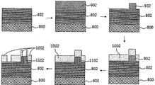
- the process 2 process is shown in FIGS. 2 and 4 (b), and the first step of growing the p-Ge layer 802 on the substrate 800, the upper layer of the p-Ge (802) layer a second step of forming an n + Ge layer using in-situ doping, and a third step of patterning and then etching the n + Ge region to form an n + Ge region 902 using the in-situ doping, wherein After the n + Ge region 902 is formed, a fourth step of forming a capping oxide film 1002 on the p-Ge layer 802, and then forming the capping oxide film 1002 for 1 hour at 600 ° C. to 700 ° C.
- the n + Ge region 1102 having the defects healed is obtained, and as shown in FIG. 4B, the capping oxide layer for forming the electrode 2402 is formed after the heat treatment.
- a sixth step of depositing an electrode is performed.
- the p-type dopant is in-situ on top of the p-Ge layer 802.
- the n + Ge layer is formed using doping, and is patterned and etched using a photoresist for forming the n + Ge region to form the n + Ge region 902.
- the formation of the capping oxide film 1002 and the heat treatment process, the formation of the electrode 2402 and the formation of the germanium 2502 are the same as those of the process 1 above.
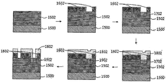
- FIGS. 3, 4 (c) and 4 (d) the process 3 process is illustrated in FIGS. 3, 4 (c) and 4 (d), and the first step of growing the p-Ge layer 1502 on the substrate 1500, the p-Ge An oxide film 1602 is deposited on top of the layer 1502 to pattern for formation of n + Ge regions, and the oxide film 1602 (Fig. 3 (a) process) or the oxide film 1602 and the p-Ge layer 1502 (Fig. Step 3 (b)), the n + Ge layer 1702 using in-situ doping of the p-type dopant over the p-Ge layer 1502 for forming the n + Ge region.
- the capping oxide film 1802 for forming the electrode 2402 after the heat treatment is performed in a fifth step of performing a heat treatment at 700 ° C. for 1 hour to 3 hours, as shown in FIGS. 4C and 4D. Patterning and depositing electrode 2402 The sixth step is made.
- an oxide film is deposited on the p-Ge layer 1502 and the n + Ge region 1702 is formed.
- the oxide layer 1602 and the p-Ge layer 1502 are deep etched, and an upper portion of the p-Ge layer 1502 is formed to form the n + Ge region 1702.
- the p-type dopant is formed in-situ doping to form an n + Ge layer.
- the formation of the capping oxide film 1802 and the heat treatment, the formation of the electrode 2402 and the formation of the germanium 2502 are the same as those of the process 1 above.
- FIG. 4 shows process 1 (FIGS. 1-4 (a)), process 2 (FIGS. 2-4 (b)), process 3 (FIGS. 3 (a)-4 (c), and FIG. 3 (b)-
- the capping oxide layers 402, 1002, and 1802 are patterned.
- the process of forming the electrode 2402 is shown at once.
- the substrate 2300, the p-Ge layer 2302, the oxide film 2304, the n + Ge region 2306, the electrode 2402, and the germanide 2406 in the electrode forming process are shown.
- Process 1 forms an n + / p junction through ion implantation.
- Process 2 forms an n + Ge layer through in situ doping, and forms an n + / p junction through selective etching of the n + Ge layer, and process 3 forms an n + Ge layer through in situ doping
- the n + / p junction is formed by etching the oxide layer and deep etching the p-Ge layer.
- low-mannide is formed through heat treatment during electrode formation.
- the processes according to each process all generate defects during the formation of the junction, but the defects can be sufficiently healed by the heat treatment process. You can proceed.
- the present invention can heal Ge defects in n + / p junctions and relatively reduce the depth of deepening through heat treatment, thereby minimizing leakage current, improving the characteristics of semiconductor devices, and increasing integration and miniaturization of semiconductor devices. It is expected to be more useful for realization.
- the process 1 process 400 nm of Ge is grown at 400 ° C. and 8 Pa on a silicon (Si) substrate, and heat treatment is performed at 825 ° C. for 30 minutes in an H 2 atmosphere. After repeating the above process once more, the Ge layer was further grown at 600 ° C. and 8 Pa, and then heat-treated in H 2 atmosphere at 750 ° C. for 15 minutes to form a p-Ge layer on the silicon substrate. Formed. After deposition and patterning of SiO 2 with an oxide film by CVD, P (phosphorus) is ion implanted with a energy of 50 keV and a dose of 10 15 cm ⁇ 2 .
- heat treatment is performed at 600 ° C. for 1 hour.
- Ti is deposited over 500 nm using CVD or an e-beam evaporator to form germanium.
- Ti begins to diffuse (diffusion) at 300 ° C or more, and begins to form germanium (germanide) at about 450 ° C heat treatment in N 2 atmosphere at 450 ° C for 1 minute.
- PH 3 phosphine
- the oxide film and the p-Ge layer are etched.
- 1% of phosphine (PH 3 ) with GeH 4 is grown in-situ in the n + Ge layer for 1 minute at 600 ° C. under a pressure of 8 Pa.
- FIG. 5 shows the results of ECV analysis according to the heat treatment temperature after intentionally generating point defects by implanting Ge ions onto the p-Ge layer.
- Point defects in Ge act as acceptor-like traps, resulting in increased p-type concentration. Therefore, it can be seen that the ECV result has a high p-type concentration for the sample that has not been heat-treated.
- the p-type concentration decreases, which can be expected to heal the defect. Therefore, it can be seen that as the heat treatment at high temperature, point defects in Ge are reduced.
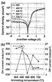
- FIG. 6 is a graph of I-V measurement versus heat treatment temperature of Ge n + / p junction.
- heat treated at low temperature 400 °C ⁇ 500 °C
- the off current increased due to the increase of point defect, but when the heat treated at high temperature (600 °C ⁇ 700 °C), off current It can be seen that is reduced to a level similar to that of the unheated sample. Therefore, when the Ge device is exposed to high temperature, it causes degradation of the device, but when heat-treated at 600 ° C or more, point defects are sufficiently healed in the next step (deposition of metal electrode using CVD, etc.). When exposed to high temperatures again, the device can be prevented from deteriorating.
- Figure 7 shows the SIMS results according to the heat treatment temperature of the Ge n + / p junction (junction), P (phosphorus, phosphorus) is not diffused up to 500 °C almost (diffusion) is seen to diffuse about 100nm at 600 °C Can be. However, at 700 ° C., it can be seen that it diffuses more than 200 nm. Therefore, from 700 ° C and above, the junction depth is greatly increased because the diffusivity of P increases rapidly. Therefore, in view of the results of the previous experiments, it is judged that heat treatment at 600 ° C. for 1 to 3 hours is most appropriate.
- the present invention is applicable to industrial fields for minimizing defects in junctions during fabrication of semiconductor devices to achieve high integration and miniaturization of semiconductor devices.
Landscapes
- Electrodes Of Semiconductors (AREA)
- Semiconductor Memories (AREA)
- Metal-Oxide And Bipolar Metal-Oxide Semiconductor Integrated Circuits (AREA)
Abstract
본 발명은 반도체 소자에서 접합 영역에서의 결함을 치유하기 위한 방법에 관한 것으로서, 기판 상에 p-Ge층을 성장시키고, 상기 p-Ge층 상층에 이온 임플란테이션을 통해 n+ Ge 영역을 형성하거나, p-Ge층 상층에 인시츄 도핑후 에칭하여 n+ Ge 영역을 형성하거나 또는 상기 p-Ge층 상층에 산화막을 증착시켜 패터닝 후 에칭하고 인시츄 도핑하여 n+ Ge층을 형성한 후, 캡핑용 산화막을 형성한 후 600℃~700℃에서 1시간 내지 3시간동안 열처리를 수행하여 전극을 증착시키는 공정을 포함하여 이루어지는 것으로, 열처리 공정을 통해 n+/p 졍션(junction)에서의 Ge 결함을 치유하고, 열처리를 통해 깊어진 졍션을 상대적으로 줄일 수 있어 누설 전류를 최소화하여 반도체 소자의 특성을 향상시키고, 반도체 소자의 고집적화 및 미세화 실현에 더욱 유용한 이점이 있다.
Description
본 발명은 반도체 소자에서 접합 영역에서의 결함을 치유하기 위한 방법에 관한 것으로서, n+ Ge 영역 형성 후에 600℃~700℃에서 1시간 내지 3시간동안 열처리를 수행하여 접합(junction, 졍션)에서의 결함을 치유하기 위한 저마늄을 이용한 반도체 소자의 접합 영역에서의 결함 치유 방법에 관한 것이다.
실리콘을 기판으로 하는 전계효과 트랜지스터는 게이트에 인가된 전압의 크기에 따라 채널영역의 변화를 통해 드레인 전류를 제어하게 되는 것으로, p형 웰(p-type well) 및 n형 소오스(n-type source) 또는 n형 드레인(n-type drain) 영역을 형성하기 위해 산화막 또는 포토레지스트를 사진식각 공정으로 정의한 후 주입되는 도펀트의 에너지를 통해 주입 깊이나 주입 농도 등을 결정하는 방법에 의해 제조된다.
상기 전계효과 트랜지스터와 같은 반도체는 실리콘 기판 상에 p형 또는 n형과 같은 서로 다른 도전형을 갖는 도전 영역을 형성하게 되는데, 이러한 도전 영역들은 필수적으로 접합(junction, 이하에서는 의미를 명확히 하기 위해 '졍션'이라고도 사용한다) 부분을 가지게 되며, 반도체 소자 제작시에 접합(junction) 부분의 결함을 최소화하는 것이 미세화된 반도체 소자의 결함을 해소하기 위한 방안으로 연구되고 있다.
이와 같이 종래의 반도체들은 필수적으로 이온을 도핑하는 과정이 수반되게 되며, 서로 다른 도전형을 갖는 접합(junction) 영역에서의 결함은 반도체 소자의 고속화 및 고집적화에 따른 미세화된 반도체 소자의 특성을 향상시키는데 걸림돌로 작용하고 있다.
따라서, 반도체 소자의 졍션에서의 결함 치유는 반도체 소자의 고집적화 및 미세화에 따른 특성 향상을 위해 매우 중요한 역할을 하게 된다.
종래 기술로는 대한민국특허청 등록특허공보 등록번호 10-0403992호 반도체 소자의 제조방법, 대한민국특허청 공개특허공보 공개번호 특2001-0068316호 모스 트랜지스터의 제조방법 등의 기술이 있다.
그러나 종래의 이러한 기술들은 졍션에서의 결함 치유를 위한 특별한 방법을 제시하고 있지 않으며, 다른 대부분의 기술들도 특별한 관심을 보이지 않고 있는 실정이다.
또한, 결함 치유를 위해서 제시된 기술에서도 특별히 온도 영역 등을 구체화하지 않고 고온에서 열처리한다라는 것으로 애매모호하게 기재하고 있어, 여전히 결함을 치유하기 위한 확실한 방법을 제공하지 못하고 있다.
또한, 높은 온도에서의 열처리를 함으로써 졍션(junction)이 깊어져 누설 전류의 발생으로 인한 열화의 가능성이 존재하며, 특히 반도체 소자가 고집적화될수록 소오스 드레인 영영의 졍션의 깊이를 줄여야만 쇼트채널 이펙트(short channel effect)에 의한 소자의 특성 저하를 방지할 수 있게 되므로, 이 부분 또한 반도체 소자의 미세화에 따른 특성 향상을 위해 해결해야 될 과제이다.
본 발명은 상기 문제점을 해결하기 위한 것으로, n+ Ge 영역 형성 후에 600℃~700℃에서 1시간 내지 3시간동안 열처리를 수행하여 졍션에서의 결함을 치유하기 위한 저마늄을 이용한 반도체 소자의 접합 영역에서의 결함 치유 방법의 제공을 그 목적으로 한다.
또한, 졍션 깊이를 줄이기 위해 전극 형성 후에 열처리를 통한 저마나이드(germanide)를 형성하여 누설 전류를 최소화하기 위한 저마늄을 이용한 반도체 소자의 접합 영역에서의 결함 치유 방법의 제공을 또 다른 목적으로 한다.
상기 목적 달성을 위해 본 발명은, 기판 상에 p-Ge층을 성장시키는 제1단계와, 상기 p-Ge층 상층에 산화막을 증착시켜, n+ Ge 영역 형성을 위한 패터닝하는 제2단계와, 상기 n+ Ge 영역 형성을 위한 패턴에 p형 도펀트를 이온 임플란테이션을 통해 n+ Ge 영역을 형성하는 제3단계와, 상기 n+ Ge 영역 형성 후에 상기 p-Ge층 상층에 캡핑용 산화막을 형성하는 제4단계와, 상기 캡핑용 산화막을 형성한 후 600℃~700℃에서 1시간 내지 3시간동안 열처리를 수행하는 제5단계와, 상기 열처리 후 전극 형성을 위한 상기 캡핑용 산화막을 패터닝하고, 전극을 증착시키는 제6단계를 포함하여 이루어진 것을 특징으로 하는 저마늄을 이용한 반도체 소자의 접합 영역에서의 결함 치유 방법을 기술적 요지로 한다.
또한, 본 발명은 기판 상에 p-Ge층을 성장시키는 제1단계와, 상기 p-Ge층 상층에 p형 도펀트를 인시츄(in-situ) 도핑을 이용하여 n+ Ge층을 형성하는 제2단계와, n+ Ge 영역 형성을 위한 패터닝한 후 에칭하여 n+ Ge 영역을 형성하는 제3단계와, 상기 n+ Ge 영역 형성 후에 상기 p-Ge층 상층에 캡핑용 산화막을 형성하는 제4단계와, 상기 캡핑용 산화막을 형성한 후 600℃~700℃에서 1시간 내지 3시간동안 열처리를 수행하는 제5단계와, 상기 열처리 후 전극 형성을 위한 상기 캡핑용 산화막을 패터닝하고, 전극을 증착시키는 제6단계를 포함하여 이루어진 것을 특징으로 하는 저마늄을 이용한 반도체 소자의 접합 영역에서의 결함 치유 방법을 또 다른 기술적 요지로 한다.
또한, 본 발명은기판 상에 p-Ge층을 성장시키는 제1단계와, 상기 p-Ge층 상층에 산화막을 증착시켜, n+ Ge 영역 형성을 위한 패터닝하고 상기 산화막 또는 상기 산화막 및 p-Ge층을 에칭하는 제2단계와 ,상기 n+ Ge 영역 형성을 위한 p-Ge층 상측으로 p형 도펀트를 인시츄(in-situ) 도핑을 이용하여 n+ Ge층을 형성하는 제3단계와, 상기 n+ Ge층 형성 후에 상기 산화막 상층에 캡핑용 산화막을 형성하는 제4단계와, 상기 캡핑용 산화막을 형성한 후 600℃~700℃에서 1시간 내지 3시간동안 열처리를 수행하는 제5단계와, 상기 열처리 후 전극 형성을 위한 상기 캡핑용 산화막을 패터닝하고, 전극을 증착시키는 제6단계를 포함하여 이루어진 것을 특징으로 하는 저마늄을 이용한 반도체 소자의 접합 영역에서의 결함 치유 방법을 또 다른 기술적 요지로 한다.
여기에서, 상기 제1단계의 p-Ge층은, 실리콘(Si) 기판 위에 350~450℃, 7.5~8.5Pa 에서 Ge을 300~500nm 성장한 후 800~150℃에서 20분~1시간 H2 분위기에서 열처리를 수행하고, 앞의 과정을 한번 더 반복한 뒤 이어서 550~650℃, 7.5~8.5Pa 에서 Ge층을 추가로 성장시키는 것이 더욱 바람직하다.
또한, 상기 제6단계의 전극은, Ti, Ni, Pd, Pt, Ta, Cu, W, Co, Zr, Cr, Mn 및 Mo 중 어느 하나를 사용하는 것이 바람직하며, 열처리를 깊어진 졍션을 줄이기 위해 전극 형성 후 400℃~500℃에서 30초~2분 동안 N2 분위기에서 열처리를 수행하여 저마나이드(germanide)층을 형성하는 것이 바람직하다.
본 발명은 반도체 소자의 정션 형성 과정에서 결함을 발생시키지만 열처리 공정을 통해 n+/p 졍션(junction)에서의 Ge 결함을 치유하고, 열처리를 통해 깊어진 졍션을 상대적으로 줄일 수 있어 누설 전류를 최소화하여 반도체 소자의 특성을 향상시키고, 반도체 소자의 고집적화 및 미세화 실현에 더욱 유용한 효과가 있다.
도 1, 도 2, 도 3 - 본 발명에 따른 3가지의 프로세스에 의한 모식도를 나타낸 도.
도 4 - 상기 프로세스에 따른 전극 형성 방법에 대한 모식도를 나타낸 도.
도 5 - p-Ge 층 위에 Ge 이온 임플란테이션을 하고 점 결함(point defect)을 의도적으로 생성시킨 후의 열처리 온도에 따른 ECV 분석 결과도.
도 6 - Ge n+/p 졍션(junction)의 열처리 온도에 따른 I-V 측정 그래프를 나타낸 도.
도 7 - Ge n+/p 졍션(junction)의 열처리 온도에 따른 SIMS 결과를 나타낸 도.
<도면에 사용된 부호에 대한 설명>
100, 800, 1500, 2300 : 기판
102, 802, 1502, 2302 : p-Ge층
202, 1602, 2304 : 산화막
302, 902, 1702, 2306 : n+ Ge 영역
402, 1002, 1802 : 캡핑용 산화막
502, 1102, 1902 : 결함치유된 n+ Ge 영역
2402 : 전극 2502: 저마나이드
본 발명은 반도체 소자에서 접합 영역에서의 결함을 치유하기 위한 방법에 관한 것으로서, 열처리 특히 n+ Ge 영역 형성 후에 600℃~700℃에서 1시간 내지 3시간동안 열처리를 수행하여 졍션에서의 결함을 치유하기 위한 것이다.
이하에서는 첨부된 도면을 참조하여 본 발명에 대해 상세히 설명하고자 한다.
도 1, 도 2, 도 3은 본 발명에 따른 3가지의 프로세스에 의한 모식도를 나타낸 도이며, 도 4는 상기 프로세스에 따른 전극 형성 방법에 대한 모식도를 나타낸 도이다.
본 발명은 크게 3가지의 프로세스(process)에 의해 구현된다.
먼저, 프로세스 1 공정은 도 1, 도 4(a)에 도시된 것으로, 기판(100) 상에 p-Ge층(102)을 성장시키는 제1단계, 상기 p-Ge층(102) 상층에 산화막(202)을 증착시켜, n+ Ge 영역(302) 형성을 위한 패터닝하는 제2단계, 상기 n+ Ge 영역(302) 형성을 위한 패턴에 p형 도펀트를 이온 임플란테이션을 통해 n+ Ge 영역(302)을 형성하는 제3단계, 상기 n+ Ge 영역(302) 형성 후에 상기 p-Ge층(102) 상층에 캡핑용 산화막(402)을 형성하는 제4단계, 상기 캡핑용 산화막(402)을 형성한 후 600℃~700℃에서 1시간 내지 3시간동안 열처리를 수행하는 제5단계 및 상기 열처리 후 전극(2402) 형성을 위한 상기 캡핑용 산화막(402)을 패터닝하고, 전극(2402)을 증착시키는 제6단계로 이루어진다.
여기에서, 상기 기판(100)은 실리콘(Si) 또는 실리콘저마늄(SiGe)을 사용한다.
상기 기판 상에 p-Ge층(102)을 성장시키게 되는데, 이는 Ge층 성장 시 특별히 n형 도펀트를 도핑하거나, Ge층 자체(intrinsic Ge, i-Ge) 만으로도 p-Ge 성질을 띄고 있어 특별히 도핑하지 않아도 무방하며, 이러한 p-Ge층 성장은 특별한 증착 방법을 한정하지 않으며, 공지된 물리적, 화학적 진공 증착법에 의해 형성된다.
상기 p-Ge층은, 상기 제1단계의 p-Ge층은, 실리콘(Si) 기판 위에 350℃~450℃, 7.5Pa~8.5Pa에서 Ge을 300~500nm 성장한 후 800℃~850℃에서 20분~1시간 동안 H2 분위기에서 열처리를 수행하고, 앞의 과정을 한 번 더 반복한 뒤 이어서 550℃~650℃, 7.5Pa~8.5Pa에서 Ge층을 추가로 성장시킨 후 700℃~800℃에서 10분~20분 동안 H2 분위기에서 열처리를 수행하여 형성시키는 방법이 바람직한데, 이는 실리콘 기판과 p-Ge층의 계면 또는 p-Ge층 내부의 결함을 최소화하기 위한 것이다.
그리고, 상기 p-Ge층(102) 성장 후에 상기 p-Ge층(102) 상층에 산화막(202)을 증착시키게 되는데, n+ Ge 영역(302) 형성을 위한 패터닝을 수행한다. 산화막(202)으로는 SiO2를 주로 사용하며, 패터닝 방법은 일반적으로 널리 사용되는 식각가스를 선택하여 반응성 이온식각장치(reactive ion etcher; RIE)를 이용하여 식각하거나 포토리소그래피 등 다른 공지된 방법을 사용한다.
그리고, 상기 n+ Ge 영역(302) 형성을 위한 패턴에 P, As, Sb와 같은 p형 도펀트를 이온 임플란테이션 방법을 통해 n+ Ge 영역(302)을 형성한 후, 열처리 과정에서 도펀트 손실과 아웃-디퓨젼(out-diffudion)을 막기 위해 캡핑용(capping) 산화막(402)을 형성한다.
그 다음, 상기 캡핑용 산화막(402) 형성 후에 600℃~700℃에서 1시간 내지 3시간동안 열처리를 수행하게 된다. 즉, 이온 임플란테이션을 통해 형성한 n+ Ge 영역을 활성화(activation)하고, 결함을 치유하기 위해 600℃~700℃에서 1시간 내지 3시간 동안 N2 분위기에서 열처리를 수행한다.
일반적으로 열처리 과정에서 도펀트의 확산이 이루어지기 때문에 낮은 온도에서 활성화를 수행하게 될 경우, Ge 내에 남아 있는 결함들이 성능 저하를 가져오기 때문에 결함을 최소화하기 위해 600℃ 이상의 고온, 바람직하게는 600℃~700℃에서 1시간 내지 3시간 동안 열처리를 수행한다. 이러한 방법에 의해 결함이 치유된 n+ Ge 영역(502)을 형성하게 된다.
그리고, 도 4(a)에 도시된 바와 같이 상기 열처리 후 전극(2402) 형성을 위한 상기 캡핑용 산화막(402)을 패터닝하고, 전극(2402)을 증착시키게 된다. 상기 전극(2402)으로는 금속을 사용하며, Ti, Ni, Pd, Pt, Ta, Cu, W, Co, Zr, Cr, Mn 및 Mo 중 어느 하나를 사용하는 것이 바람직하다. 전극 증착법으로는 CVD와 같은 물리적, 화학적 진공 증착법을 사용하며, 전극 증착후 상기 산화막과 동일한 방법으로 전극 패터닝을 수행하게 된다.
이러한 전극(2402) 증착 후 열처리를 함으로써 저마나이드(germanide)(2502)를 형성하게 되는데, 형성된 저마나이드(germanide)(2502)는 Ge 내의 결함을 최소화하기 위해 높은 온도에서, 바람직하게는 400℃~500℃에서 30초~2분 동안 N2 분위기에서 열처리를 수행한다.
이는 저마나이드(germanide)(2502)의 형성을 통해 Ge 내의 결함을 최소화하고, 높은 온도에서 열처리를 수행함으로써 발생한 깊어진 졍션(junction)을 보상하는 역할을 하게 된다. 즉, 저마나이드(germanide)(2502)의 형성을 통해 저항도가 낮은 물질이 깊어진 졍션만큼 안으로 들어감으로써 졍션 깊이를 상대적으로 줄이게 되는 것이다.
다음으로, 프로세스 2공정은 도 2, 도 4(b)에 도시된 것으로, 기판(800) 상에 p-Ge층(802)을 성장시키는 제1단계, 상기 p-Ge(802)층 상층에 p형 도펀트를 인시츄(in-situ) 도핑을 이용하여 n+ Ge층을 형성하는 제2단계, n+ Ge 영역 형성을 위한 패터닝한 후 에칭하여 n+ Ge 영역(902)을 형성하는 제3단계, 상기 n+ Ge 영역(902) 형성 후에 상기 p-Ge층(802) 상층에 캡핑용 산화막(1002)을 형성하는 제4단계, 상기 캡핑용 산화막(1002)을 형성한 후 600℃~700℃에서 1시간 내지 3시간동안 열처리를 수행하는 제5단계로 결함이 치유된 n+ Ge 영역(1102)을 얻고, 도 4(b)에 도시된 바와 같이 상기 열처리 후 전극(2402) 형성을 위한 상기 캡핑용 산화막을 패터닝한 후, 전극을 증착시키는 제6단계로 이루어지는 것이다.
여기에서, 프로세스 1공정과 대체적으로 유사하나 제1단계의 기판(800) 상에 p-Ge층(802) 성장 후에, p-Ge층(802) 상층에 p형 도펀트를 인시츄(in-situ) 도핑을 이용하여 n+ Ge층을 형성하고, n+ Ge 영역 형성을 위한 포토레지스트를 이용하여 패터닝한 후 에칭하여 n+ Ge 영역(902)을 형성하게 된다.
그 다음 캡핑용 산화막(1002) 형성과 열처리 과정 및 전극(2402) 형성 및 저마나이드(germanide)(2502) 형성은 상기 프로세스 1 공정과 동일하다.
다음으로, 프로세스 3공정은 도 3 및 도 4(c),도 4(d)에 도시된 것으로, 기판(1500) 상에 p-Ge층(1502)을 성장시키는 제1단계, 상기 p-Ge층(1502) 상층에 산화막(1602)을 증착시켜, n+ Ge 영역 형성을 위한 패터닝하고 상기 산화막(1602)(도 3(a) 공정) 또는 산화막(1602) 및 p-Ge층(1502)(도 3(b) 공정)을 에칭하는 제2단계, 상기 n+ Ge 영역 형성을 위한 p-Ge층(1502) 상측으로 p형 도펀트를 인시츄(in-situ) 도핑을 이용하여 n+ Ge층(1702)을 형성하는 제3단계, 상기 n+ Ge층(1702) 형성 후에 상기 산화막(1602) 상층에 캡핑용 산화막(1802)을 형성하는 제4단계, 상기 캡핑용 산화막(1802)을 형성한 후 600℃~700℃에서 1시간 내지 3시간동안 열처리를 수행하는 제5단계, 도 4(c), 도 4(d)에 도시된 바와 같이 상기 열처리 후 전극(2402) 형성을 위한 상기 캡핑용 산화막(1802)을 패터닝하고, 전극(2402)을 증착시키는 제6단계로 이루어진다.
여기에서, 프로세스 1공정과 대체적으로 유사하나 제1단계의 기판(1500) 상에 p-Ge층(1502) 성장 후에, p-Ge층(1502) 상층에 산화막을 증착시키고, n+ Ge 영역(1702) 형성을 위한 패터닝한 후, 상기 산화막(1602) 및 p-Ge층(1502)을 딥에칭(deep etching))하고, 상기 n+ Ge 영역(1702) 형성을 위한 p-Ge층(1502) 상측으로 p형 도펀트를 인시츄(in-situ) 도핑을 이용하여 n+ Ge층을 형성한다.
그 다음 캡핑용 산화막(1802) 형성과 열처리 과정 및 전극(2402) 형성 및 저마나이드(germanide)(2502) 형성은 상기 프로세스 1 공정과 동일하다.
도 4는 프로세스 1(도 1-도 4(a)), 프로세스 2(도 2-도 4(b)), 프로세스 3(도 3(a)-도 4(c),도 3(b)-도 4(d))에서 형성된 열처리하여 결함이 치유된 n+ Ge 영역(502),(1102),(1902)을 갖는 소자에서, 상기 캡핑용 산화막(402), (1002), (1802)을 패터닝하고, 전극(2402)을 형성하는 과정을 한꺼번에 나타낸 것이다. 전극 형성 프로세스에서의 기판(2300), p-Ge층(2302), 산화막(2304), n+ Ge 영역(2306), 전극(2402), 저마나이드(2406)를 도시한 것이다.
이와 같이 본 발명에 따른 저마늄을 이용한 반도체 소자의 접합 영역에서의 결함 치유 방법은 크게 3가지의 프로세스에 의해 진행되게 되는데, 프로세스 1은 이온 임플란테이션을 통해 n+/p 졍션(junction)을 형성하고, 프로세스 2는 인시츄 도핑을 통해 n+ Ge층을 형성하고, n+ Ge층의 선택적 에칭을 통해 n+/p 졍션(junction)을 형성하며, 프로세스 3은 인시츄 도핑을 통해 n+ Ge층을 형성하고, 산화막 에칭 및 p-Ge층의 딥에칭(deep etching)을 통해 n+/p 졍션(junction)을 형성하는 것이다.
그리고, 상기의 이온 임플란테이션 또는 인시츄 도핑 과정을 통해 형성된 n+/p 졍션(junction)에서 깊어진 졍션을 줄이기 위해 전극 형성시 열처리를 통해 저마나이드(germanide)를 형성하는 것이다.
이와 같이 각 프로세스에 따른 공정은 모두 정션 형성 과정에서 결함을 발생시키지만 열처리 공정을 통해 결함을 충분히 치유(healing)시킬 수 있으며, 따라서 각 소자에 따른 적절한 프로세스에 따른 반도체 소자의 구조를 선택하여 공정을 진행하면 된다.
이에 의해 본 발명은 n+/p 졍션(junction)에서의 Ge 결함을 치유하고, 열처리를 통해 깊어진 졍션을 상대적으로 줄일 수 있어 누설 전류를 최소화하여 반도체 소자의 특성을 향상시키고, 반도체 소자의 고집적화 및 미세화 실현에 더욱 유용할 것으로 기대된다.
이하에서는 본 발명의 일실시예에 대해 살펴보고자 하며, 설명하지 않은 부분은 일반적인 공정방법을 사용한다.
먼저, 프로세스 1공정은 실리콘(Si) 기판 위에 400℃, 8 Pa 에서 Ge을 400nm 성장한 후 825℃에서 30분간 H2 분위기에서 열처리를 수행한다. 그리고 앞의 과정을 한 번 더 반복한 뒤 이어서 600℃, 8 Pa 에서 Ge층을 추가로 성장시킨 후, 750℃에서 15분간 H2 분위기에서 열처리를 수행하여, 실리콘 기판 상에 p-Ge층을 형성시켰다. 그리고, CVD법으로 산화막으로 SiO2 증착 및 패터닝한 후, P(phosphorus)를 50keV의 에너지와 1015cm-2의 도스량(dose)으로 이온 임플란테이션한다.
그리고, 앞의 산화막과 동일한 SiO2 캡핑용 산화막을 증착한 후 포토리소그래피나 이온 식각 공정을 통해 패터닝한 후, 600℃에서 1시간동안 열처리를 수행한다.
상기 열처리 후 저마나이드(germanide)를 형성하기 위해 Ti를 CVD 또는 e-beam evaporator를 이용하여 500nm 이상 증착한다. Ti는 300℃ 이상에서 확산(diffusion)하기 시작하고, 약 450℃에서 저마나이드(germanide)를 형성하기 시작하기 때문에 450℃에서 1분 동안 N2 분위기에서 열처리를 한다.
다음으로 프로세스 2 공정은, 상기 프로세스 1공정과 유사하며, 제2단계 및 제3단계는 1%의 phosphine(PH3)를 GeH4와 함께 600℃에서 8Pa의 압력 하에서 1분 동안 n+ Ge층을 인시츄(in-situ) 성장한다. 포토레지스트를 스핀 코팅한 후 포토리소그래피를 이용하여 패터닝을 수행한 후, NH4OH : H2O2 : H2O = 1: 1: 7 을 이용하여 Ge을 60초 동안 에칭하고, 포토레지스트를 제거하여 n+ Ge 영역을 형성한다.
다음으로 프로세스 3 공정은, 프로세스 1공정과 유사하며, 제2단계 및 제3단계는 NH4OH : H2O2 : H2O = 1: 1: 7을 이용하여 n+ Ge 층을 100초 동안 산화막 및 p-Ge층을 에칭한다. 1%의 phosphine(PH3)를 GeH4와 함께 600℃에서 8Pa의 압력하에서 1분 동안 n+ Ge층을 인시츄(in-situ) 성장한다.
이하에서는 상기의 실시예 중 프로세스 1에 의해 형성된 반도체 소자에 대한 실험 데이타 및 이를 통해 그 효과를 입증하고자 한다.
도 5는 p-Ge 층 위에 Ge 이온을 임플란테이션함으로써 점 결함(point defect)을 의도적으로 생성시킨 후 열처리 온도에 따른 ECV 분석 결과를 나타낸 것이다. Ge 내에서 점 결함(point defect(vacancy))는 받개 유사 트랩(acceptor-like trap)으로써 작용하기 때문에 p-type 농도(concentration)가 증가하게 된다. 따라서 열처리 하지 않은 샘플에 대해 ECV 결과 값이 높은 p-type 농도(concentration)를 가지는 것을 볼 수 있다. 그리고 열처리 온도가 증가함에 따라 p-type 농도(concentration)가 감소하는 것으로 보아 결함이 치유되는 것으로 예상할 수 있다. 따라서, 고온에서 열처리 할수록 Ge 내의 점 결함(point defect)이 감소된다는 것을 알 수 있다.
도 6은 Ge n+/p 졍션(junction)의 열처리 온도에 따른 I-V 측정 그래프입니다. 저온(400℃~500℃)에서 열처리 하였을 때는 점 결함(point defect)의 증가로 인해 오프 전류(off current)가 증가하였으나, 고온(600℃~700℃)에서 열처리 하였을 때는 오프 전류(off current)가 열처리 하지 않은 샘플과 비슷한 수준으로 감소되었음을 알 수 있다. 따라서 Ge 소자가 높은 온도에 노출되게 되면 소자의 열화(degradation)가 생기지만 600℃ 이상에서 열처리하였을 때는 점 결함(point defect)이 충분히 치유되어짐으로써 다음 공정(CVD를 이용한 금속 전극 증착 등) 단계에서 다시 고온에 노출되었을 때 소자의 열화를 막을 수 있게 되는 것이다.
도 7은 Ge n+/p 졍션(junction)의 열처리 온도에 따른 SIMS 결과를 나타낸 것으로, 500℃까지는 P(phosphorus, 인)가 거의 확산(diffusion)되지 않다가 600℃에서는 약 100nm 정도 확산되는 것을 볼 수 있다. 그러나 700℃에서는 200nm 이상 확산되는 것을 볼 수 있다. 따라서 700℃ 이상부터는 P의 확산도(diffusivity)가 급격하게 증가하기 때문에 졍션 깊이(junction depth)가 크게 증가하게 됩니다. 따라서, 앞의 실험들의 결과를 종합해 보았을 때 600℃에서 1~3시간 열처리를 하는 것이 가장 적절한 것으로 판단된다.
본 발명은 반도체 소자 제작시 졍션(junction)에서의 결함을 최소화하여 반도체 소자의 고집적화 및 미세화하기 위한 산업 분야에 이용 가능성이 있다.
Claims (12)
- 기판 상에 p-Ge층을 성장시키는 제1단계와;
상기 p-Ge층 상층에 산화막을 증착시켜, n+ Ge 영역 형성을 위한 패터닝하는 제2단계와;
상기 n+ Ge 영역 형성을 위한 패턴에 p형 도펀트를 이온 임플란테이션을 통해 n+ Ge 영역을 형성하는 제3단계와;
상기 n+ Ge 영역 형성 후에 상기 p-Ge층 상층에 캡핑용 산화막을 형성하는 제4단계와;
상기 캡핑용 산화막을 형성한 후 600℃~700℃에서 1시간 내지 3시간동안 열처리를 수행하는 제5단계와;
상기 열처리 후 전극 형성을 위한 상기 캡핑용 산화막을 패터닝하고, 전극을 증착시킨 후 열처리하는 제6단계;를 포함하여 이루어진 것을 특징으로 하는 저마늄을 이용한 반도체 소자의 접합 영역에서의 결함 치유 방법. - 제 1항에 있어서, 상기 제1단계의 p-Ge층은,
실리콘(Si) 기판 위에 350℃~450℃, 7.5Pa~8.5Pa에서 Ge을 300~500nm 성장한 후 800℃~850℃에서 20분~1시간 동안 H2 분위기에서 열처리를 수행하고, 앞의 과정을 한 번 더 반복한 뒤 이어서 550℃~650℃, 7.5Pa~8.5Pa에서 Ge층을 추가로 성장시킨 후 700℃~800℃에서 10분~20분 동안 H2 분위기에서 열처리를 수행하여 형성시킨 것을 특징으로 하는 저마늄을 이용한 반도체 소자의 접합 영역에서의 결함 치유 방법. - 제 1항에 있어서, 상기 제6단계의 전극은,
Ti, Ni, Pd, Pt, Ta, Cu, W, Co, Zr, Cr, Mn 및 Mo 중 어느 하나를 사용하는 것을 특징으로 하는 저마늄을 이용한 반도체 소자의 접합 영역에서의 결함 치유 방법. - 제 1항에 있어서, 상기 제6단계의 전극 증착 후,
400℃~500℃에서 30초~2분 동안 N2 분위기에서 열처리를 수행하여 저마나이드(germanide)층을 형성하는 것을 특징으로 하는 저마늄을 이용한 반도체 소자의 접합 영역에서의 결함 치유 방법. - 기판 상에 p-Ge층을 성장시키는 제1단계와;
상기 p-Ge층 상층에 p형 도펀트를 인시츄(in-situ) 도핑을 이용하여 n+ Ge층을 형성하는 제2단계와;
n+ Ge 영역 형성을 위한 패터닝한 후 에칭하여 n+ Ge 영역을 형성하는 제3단계와;
상기 n+ Ge 영역 형성 후에 상기 p-Ge층 상층에 캡핑용 산화막을 형성하는 제4단계와;
상기 캡핑용 산화막을 형성한 후 600℃~700℃에서 1시간 내지 3시간동안 열처리를 수행하는 제5단계와;
상기 열처리 후 전극 형성을 위한 상기 캡핑용 산화막을 패터닝하고, 전극을 증착시킨 후 열처리하는 제6단계;를 포함하여 이루어진 것을 특징으로 하는 저마늄을 이용한 반도체 소자의 접합 영역에서의 결함 치유 방법. - 제 5항에 있어서, 상기 상기 제1단계의 p-Ge층은,
실리콘(Si) 기판 위에 350℃~450℃, 7.5Pa~8.5Pa에서 Ge을 300~500nm 성장한 후 800℃~850℃에서 20분~1시간 동안 H2 분위기에서 열처리를 수행하고, 앞의 과정을 한 번 더 반복한 뒤 이어서 550℃~650℃, 7.5Pa~8.5Pa에서 Ge층을 추가로 성장시킨 후 700℃~800℃에서 10분~20분 동안 H2 분위기에서 열처리를 수행하여 형성시킨 것을 특징으로 하는 저마늄을 이용한 반도체 소자의 접합 영역에서의 결함 치유 방법. - 제 5항에 있어서, 상기 제6단계의 전극은,
Ti, Ni, Pd, Pt, Ta, Cu, W, Co, Zr, Cr, Mn 및 Mo 중 어느 하나를 사용하는 것을 특징으로 하는 저마늄을 이용한 반도체 소자의 접합 영역에서의 결함 치유 방법. - 제 5항에 있어서, 상기 제6단계의 전극 증착 후,
400℃~500℃에서 30초~2분 동안 N2 분위기에서 열처리를 수행하여 저마나이드(germanide)층을 형성하는 것을 특징으로 하는 저마늄을 이용한 반도체 소자의 접합 영역에서의 결함 치유 방법. - 기판 상에 p-Ge층을 성장시키는 제1단계와;
상기 p-Ge층 상층에 산화막을 증착시켜, n+ Ge 영역 형성을 위한 패터닝하고 상기 산화막 또는 상기 산화막 및 p-Ge층을 에칭하는 제2단계와;
상기 n+ Ge 영역 형성을 위한 p-Ge층 상측으로 p형 도펀트를 인시츄(in-situ) 도핑을 이용하여 n+ Ge층을 형성하는 제3단계와;
상기 n+ Ge층 형성 후에 상기 산화막 상층에 캡핑용 산화막을 형성하는 제4단계와;
상기 캡핑용 산화막을 형성한 후 600℃~700℃에서 1시간 내지 3시간동안 열처리를 수행하는 제5단계와;
상기 열처리 후 전극 형성을 위한 상기 캡핑용 산화막을 패터닝하고, 전극을 증착시킨 후 열처리하는 제6단계;를 포함하여 이루어진 것을 특징으로 하는 저마늄을 이용한 반도체 소자의 접합 영역에서의 결함 치유 방법. - 제 9항에 있어서, 상기 상기 제1단계의 p-Ge층은,
실리콘(Si) 기판 위에 350℃~450℃, 7.5Pa~8.5Pa에서 Ge을 300~500nm 성장한 후 800℃~850℃에서 20분~1시간 동안 H2 분위기에서 열처리를 수행하고, 앞의 과정을 한 번 더 반복한 뒤 이어서 550℃~650℃, 7.5Pa~8.5Pa에서 Ge층을 추가로 성장시킨 후 700℃~800℃에서 10분~20분 동안 H2 분위기에서 열처리를 수행하여 형성시킨 것을 특징으로 하는 저마늄을 이용한 반도체 소자의 접합 영역에서의 결함 치유 방법. - 제 9항에 있어서, 상기 제6단계의 전극은,
Ti, Ni, Pd, Pt, Ta, Cu, W, Co, Zr, Cr, Mn 및 Mo 중 어느 하나를 사용하는 것을 특징으로 하는 저마늄을 이용한 반도체 소자의 접합 영역에서의 결함 치유 방법. - 제 9항에 있어서, 상기 제6단계의 전극 증착 후,
400℃~500℃에서 30초~2분 동안 N2 분위기에서 열처리를 수행하여 저마나이드(germanide)층을 형성하는 것을 특징으로 하는 저마늄을 이용한 반도체 소자의 접합 영역에서의 결함 치유 방법.
Applications Claiming Priority (2)
| Application Number | Priority Date | Filing Date | Title |
|---|---|---|---|
| KR10-2012-0157977 | 2012-12-31 | ||
| KR1020120157977A KR101419533B1 (ko) | 2012-12-31 | 2012-12-31 | 저마늄을 이용한 반도체 소자의 접합 영역에서의 결함 치유 방법 |
Publications (1)
| Publication Number | Publication Date |
|---|---|
| WO2014104552A1 true WO2014104552A1 (ko) | 2014-07-03 |
Family
ID=51017641
Family Applications (1)
| Application Number | Title | Priority Date | Filing Date |
|---|---|---|---|
| PCT/KR2013/009502 Ceased WO2014104552A1 (ko) | 2012-12-31 | 2013-10-24 | 저마늄을 이용한 반도체 소자의 접합 영역에서의 결함 치유 방법 |
Country Status (3)
| Country | Link |
|---|---|
| US (1) | US8999825B2 (ko) |
| KR (1) | KR101419533B1 (ko) |
| WO (1) | WO2014104552A1 (ko) |
Families Citing this family (2)
| Publication number | Priority date | Publication date | Assignee | Title |
|---|---|---|---|---|
| KR102225183B1 (ko) | 2019-06-05 | 2021-03-10 | 인천대학교 산학협력단 | 선택적 증착에 의한 메모리 소자 결함 회복 방법 |
| US11088147B2 (en) | 2019-06-26 | 2021-08-10 | Micron Technology, Inc. | Apparatus with doped surfaces, and related methods with in situ doping |
Citations (1)
| Publication number | Priority date | Publication date | Assignee | Title |
|---|---|---|---|---|
| US20060019466A1 (en) * | 2004-07-22 | 2006-01-26 | Nayfeh Ammar M | Germanium substrate-type materials and approach therefor |
Family Cites Families (4)
| Publication number | Priority date | Publication date | Assignee | Title |
|---|---|---|---|---|
| EP1192647B1 (en) * | 1999-06-25 | 2010-10-20 | Massachusetts Institute Of Technology | Oxidation of silicon on germanium |
| US7008813B1 (en) * | 2005-02-28 | 2006-03-07 | Sharp Laboratories Of America, Inc.. | Epitaxial growth of germanium photodetector for CMOS imagers |
| US7361528B2 (en) * | 2005-02-28 | 2008-04-22 | Sharp Laboratories Of America, Inc. | Germanium infrared sensor for CMOS imagers |
| KR101186291B1 (ko) * | 2005-05-24 | 2012-09-27 | 삼성전자주식회사 | 게르마늄 온 인슐레이터 구조 및 이를 이용한 반도체 소자 |
-
2012
- 2012-12-31 KR KR1020120157977A patent/KR101419533B1/ko not_active Expired - Fee Related
-
2013
- 2013-10-24 WO PCT/KR2013/009502 patent/WO2014104552A1/ko not_active Ceased
- 2013-11-21 US US14/086,320 patent/US8999825B2/en active Active
Patent Citations (1)
| Publication number | Priority date | Publication date | Assignee | Title |
|---|---|---|---|---|
| US20060019466A1 (en) * | 2004-07-22 | 2006-01-26 | Nayfeh Ammar M | Germanium substrate-type materials and approach therefor |
Non-Patent Citations (3)
| Title |
|---|
| CHUI; CHI ON ET AL.: "German ium n-type shallow junction activation dependences", APPLIED PHYSICS LETTERS, vol. 87, 2005, pages 091909 1 - 3 * |
| YU ; D.S. ET AL.: "A12O3-Ge-On-Insulator n- and p-MOSFETs With Fully NiSi and NiGe Dual Gates", IEEE ELECTRON DEVICE LETTERS, vol. 25, 2004, pages 138 - 140 * |
| YU ; HYUN-YONG ET AL.: "High Performance n-MOSFETs with Novel Source/Drain on Selectively Grown Ge on Si for Monolithic Integration", IEDM, 2009, pages 1 - 4 * |
Also Published As
| Publication number | Publication date |
|---|---|
| US8999825B2 (en) | 2015-04-07 |
| US20140187021A1 (en) | 2014-07-03 |
| KR101419533B1 (ko) | 2014-07-14 |
| KR20140087549A (ko) | 2014-07-09 |
Similar Documents
| Publication | Publication Date | Title |
|---|---|---|
| KR100954874B1 (ko) | 채널 영역에서 레트로그레이드 도펀트 프로필을 구비한반도체 디바이스 및 그 제조 방법 | |
| US8187959B2 (en) | Semiconductor substrate with solid phase epitaxial regrowth with reduced junction leakage and method of producing same | |
| JP4597531B2 (ja) | チャネル領域のドーパント分布がレトログレードな半導体デバイスおよびそのような半導体デバイスの製造方法 | |
| CN113421914B (zh) | p型金属氧化物电流阻挡层Ga2O3垂直金属氧化物半导体场效应晶体管 | |
| US6537885B1 (en) | Transistor and method of manufacturing a transistor having a shallow junction formation using a two step EPI layer | |
| CN101399288B (zh) | 一种ldmos芯片的轻掺杂漂移区结构形成方法 | |
| US20040266116A1 (en) | Methods of fabricating semiconductor structures having improved conductivity effective mass | |
| US7785979B2 (en) | Integrated circuits comprising resistors having different sheet resistances and methods of fabricating the same | |
| US20100109046A1 (en) | Methods of forming low interface resistance contacts and structures formed thereby | |
| JP3992211B2 (ja) | Cmosfetの製造方法 | |
| CN1922717A (zh) | 用于半导体制造的栅极掺杂物激活方法 | |
| JP2009272423A (ja) | 半導体装置及びその製造方法 | |
| US8318571B2 (en) | Method for forming P-type lightly doped drain region using germanium pre-amorphous treatment | |
| JP5910965B2 (ja) | トンネル電界効果トランジスタの製造方法及びトンネル電界効果トランジスタ | |
| JP2003158250A (ja) | SiGe/SOIのCMOSおよびその製造方法 | |
| US20170278949A1 (en) | Stress memorization and defect suppression techniques for nmos transistor devices | |
| KR101419533B1 (ko) | 저마늄을 이용한 반도체 소자의 접합 영역에서의 결함 치유 방법 | |
| US9741853B2 (en) | Stress memorization techniques for transistor devices | |
| US6989302B2 (en) | Method for fabricating a p-type shallow junction using diatomic arsenic | |
| CN100401476C (zh) | 半导体器件的制造方法 | |
| CN100474513C (zh) | 一种制造半导体器件的方法及用该方法制造的半导体器件 | |
| US20040115889A1 (en) | Ultra shallow junction formation | |
| US20050112830A1 (en) | Ultra shallow junction formation | |
| CN115763233A (zh) | 一种SiC MOSFET的制备方法 | |
| CN1934686A (zh) | 场效应晶体管及场效应晶体管的制造方法 |
Legal Events
| Date | Code | Title | Description |
|---|---|---|---|
| 121 | Ep: the epo has been informed by wipo that ep was designated in this application |
Ref document number: 13868394 Country of ref document: EP Kind code of ref document: A1 |
|
| NENP | Non-entry into the national phase |
Ref country code: DE |
|
| 32PN | Ep: public notification in the ep bulletin as address of the adressee cannot be established |
Free format text: NOTING OF LOSS OF RIGHTS PURSUANT TO RULE 112(1) EPC (EPO FORM 1205A DATED 10/11/2015) |
|
| 122 | Ep: pct application non-entry in european phase |
Ref document number: 13868394 Country of ref document: EP Kind code of ref document: A1 |