WO2014103598A1 - 電子機器 - Google Patents
電子機器 Download PDFInfo
- Publication number
- WO2014103598A1 WO2014103598A1 PCT/JP2013/081893 JP2013081893W WO2014103598A1 WO 2014103598 A1 WO2014103598 A1 WO 2014103598A1 JP 2013081893 W JP2013081893 W JP 2013081893W WO 2014103598 A1 WO2014103598 A1 WO 2014103598A1
- Authority
- WO
- WIPO (PCT)
- Prior art keywords
- load
- voltage
- unit
- group
- load unit
- Prior art date
- Legal status (The legal status is an assumption and is not a legal conclusion. Google has not performed a legal analysis and makes no representation as to the accuracy of the status listed.)
- Ceased
Links
Images





Classifications
-
- G—PHYSICS
- G01—MEASURING; TESTING
- G01R—MEASURING ELECTRIC VARIABLES; MEASURING MAGNETIC VARIABLES
- G01R31/00—Arrangements for testing electric properties; Arrangements for locating electric faults; Arrangements for electrical testing characterised by what is being tested not provided for elsewhere
- G01R31/44—Testing lamps
-
- H—ELECTRICITY
- H05—ELECTRIC TECHNIQUES NOT OTHERWISE PROVIDED FOR
- H05B—ELECTRIC HEATING; ELECTRIC LIGHT SOURCES NOT OTHERWISE PROVIDED FOR; CIRCUIT ARRANGEMENTS FOR ELECTRIC LIGHT SOURCES, IN GENERAL
- H05B45/00—Circuit arrangements for operating light-emitting diodes [LED]
- H05B45/30—Driver circuits
- H05B45/37—Converter circuits
- H05B45/3725—Switched mode power supply [SMPS]
-
- H—ELECTRICITY
- H05—ELECTRIC TECHNIQUES NOT OTHERWISE PROVIDED FOR
- H05B—ELECTRIC HEATING; ELECTRIC LIGHT SOURCES NOT OTHERWISE PROVIDED FOR; CIRCUIT ARRANGEMENTS FOR ELECTRIC LIGHT SOURCES, IN GENERAL
- H05B45/00—Circuit arrangements for operating light-emitting diodes [LED]
- H05B45/40—Details of LED load circuits
- H05B45/44—Details of LED load circuits with an active control inside an LED matrix
- H05B45/46—Details of LED load circuits with an active control inside an LED matrix having LEDs disposed in parallel lines
-
- H—ELECTRICITY
- H05—ELECTRIC TECHNIQUES NOT OTHERWISE PROVIDED FOR
- H05B—ELECTRIC HEATING; ELECTRIC LIGHT SOURCES NOT OTHERWISE PROVIDED FOR; CIRCUIT ARRANGEMENTS FOR ELECTRIC LIGHT SOURCES, IN GENERAL
- H05B45/00—Circuit arrangements for operating light-emitting diodes [LED]
- H05B45/50—Circuit arrangements for operating light-emitting diodes [LED] responsive to malfunctions or undesirable behaviour of LEDs; responsive to LED life; Protective circuits
- H05B45/58—Circuit arrangements for operating light-emitting diodes [LED] responsive to malfunctions or undesirable behaviour of LEDs; responsive to LED life; Protective circuits involving end of life detection of LEDs
-
- G—PHYSICS
- G01—MEASURING; TESTING
- G01R—MEASURING ELECTRIC VARIABLES; MEASURING MAGNETIC VARIABLES
- G01R31/00—Arrangements for testing electric properties; Arrangements for locating electric faults; Arrangements for electrical testing characterised by what is being tested not provided for elsewhere
- G01R31/26—Testing of individual semiconductor devices
- G01R31/2607—Circuits therefor
- G01R31/2632—Circuits therefor for testing diodes
- G01R31/2635—Testing light-emitting diodes, laser diodes or photodiodes
Definitions
- the present invention relates to an electronic device including a plurality of elements such as light emitting diodes (hereinafter referred to as LEDs).
- LEDs light emitting diodes
- Patent Document 1 proposes an illumination device including a circuit for detecting an abnormality of an LED.
- FIG. 10 is a block diagram showing a conventional lighting device.
- the lighting device 100 includes X LED arrays 1011 to 101X (X is a natural number of 2 or more) formed by connecting a plurality of LEDs 200 in series, a power source 102 that supplies power to the LEDs 200, A reference voltage generation unit 103 that divides the power supply voltage 102 to generate a reference voltage, and X resistors that are connected in series to the LED strings 1011 to 101X and generate detection voltages according to the currents flowing through the LED strings 1011 to 101X Devices 1041 to 104X, and X comparison units 1051 to 105X that compare the detection voltage and the reference voltage for each of the LED arrays 1011 to 101X and output an output signal COUT.
- X is a natural number of 2 or more
- the comparison units 1051 to 105X corresponding to the LED arrays 1011 to 101X in which an abnormality has occurred include the LED array 1011.
- An output signal COUT indicating that there is an abnormality in .about.101X is output.
- the same number of comparison units 1051 to 105X as the LED rows 1011 to 101X are required, so that the circuit scale is remarkably increased and the cost is increased.
- an object of the present invention is to provide an electronic device capable of detecting an element abnormality with a simple configuration.
- the present invention provides a first element array group in which at least one element array in which at least one element is connected in series is connected in parallel, and at least one element array in parallel connection.
- a first current that is a sum of currents flowing through the element rows that constitute the first element row group, and a current that flows through the element rows that constitute the second element row group.
- An abnormality detection unit that detects an abnormality of the element array that constitutes at least one of the first element array group and the second element array group based on whether a second current satisfies a predetermined relationship. And providing an electronic device.
- the abnormality detection unit includes a first load unit that has one end connected to the first element array group and outputs a first voltage that is a voltage corresponding to the first current from the one end. And a second load portion that is connected to the second element array group and outputs a second voltage that is a voltage corresponding to the second current from the one end, and the magnitude of the first voltage and the second voltage.
- a comparison unit that detects an abnormality of the element row belonging to at least one of the first element row group and the second element row group by comparing, and the other end of the first load portion;
- the other end of the second load unit is connected, and the ratio of the resistance value of the first load unit and the resistance value of the second load unit is the parallel number of the element rows forming the second element row group. It is preferable that the ratio is in parallel with the number of parallel elements arranged in the first element array group.
- each of the first load unit and the second load unit includes at least one resistor connected in parallel, and the number of the resistors in parallel forming the first load unit.
- the parallel number of the resistors forming the second load unit is calculated by: a parallel number of the element arrays forming the first element array group and a parallel number of the element arrays forming the second element array group You may make it become ratio.
- each of the first load unit and the second load unit includes at least one transistor in which the one end is the first electrode and the other end is the second electrode connected in parallel.
- the control electrodes of the transistors constituting the first load part and the second load part are connected to each other, and the control electrode of the at least one transistor constituting the first load part and the first
- the ratio of the parallel number of the transistors forming the first load unit and the parallel number of the transistors forming the second load unit, to which the electrode is connected, is the parallel number of the element columns forming the first element column group And the parallel number of the element rows forming the second element row group.
- the transistor may be an NPN bipolar transistor in which the first electrode is a collector, the second electrode is an emitter, and the control electrode is a base.
- the electronic device having the above characteristics may further include an offset load unit connected in parallel to at least one of the first load unit and the second load unit.
- each of the element arrays constituting the first element array group and the second element array group has an equal current-voltage characteristic
- the abnormality detection unit includes the first current array.
- the second current exceeds a predetermined degree from the ratio of the parallel number of the element rows forming the first element row group and the parallel number of the element rows forming the second element row group. It is preferable to detect an abnormality in the element row that constitutes at least one of the first element row group and the second element row group when there is a divergence.
- the illumination device having the above characteristics, it is possible to detect an abnormality in the element array only by including an abnormality detection unit that detects that the relationship between the first current and the second current is abnormal. Therefore, it is possible to detect an abnormality in the element array with a simple configuration without providing a device for detecting an abnormality in each element array.
- the block diagram shown about the example of a whole structure of the illuminating device which concerns on embodiment of this invention.
- the block diagram shown about the structural example of the abnormality detection part shown in FIG. The circuit diagram shown about the 1st example of the concrete circuit structure of the 1st load part shown in FIG. 2, and a 2nd load part.
- the circuit diagram shown about the 2nd example of the concrete circuit structure of the comparison part shown in FIG. The circuit diagram shown about the 1st another example of the concrete circuit structure of the abnormality detection part shown in FIG.
- the circuit diagram shown about the 2nd example of a concrete circuit structure of the abnormality detection part shown in FIG. The block diagram shown about another example of the alignment method of LED.
- a lighting device capable of detecting an LED abnormality will be described as an example.
- the illumination device described below is only one embodiment of the electronic apparatus according to the present invention.
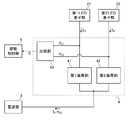
- FIG. 1 is a block diagram showing an example of the overall configuration of a lighting apparatus according to an embodiment of the present invention.
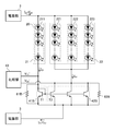
- the lighting device 1 includes a first LED element array group 21 (first element array group), a second LED element array group 22 (second element array group), a power supply unit 3, and an abnormality detection unit. 4 and a drive control unit 5.
- the first LED element array group 21 is composed of m LED element arrays 211 to 21m (element arrays) (m is a natural number).
- the second LED element array group 22 includes n LED element arrays 221 to 22n (n is a natural number).
- the LED element rows 211 to 21m and 221 to 22n are composed of at least one LED 20 (element) connected in series.
- the power supply unit 3 supplies power (for example, DC power or PWM-controlled pulse power) to the LED element arrays 211 to 21m and 221 to 22n.
- power for example, DC power or PWM-controlled pulse power
- the abnormality detection unit 4 flows through the first current I 21 which is the sum of the currents flowing through the LED element arrays 211 to 21m forming the first LED element array group 21 and the LED element arrays 221 to 22n forming the second LED element array group 22. Based on whether or not the second current I 22 that is the sum of the currents satisfies a predetermined relationship, the LED element rows 211 to 211 that form at least one of the first LED element row group 21 and the second LED element row group 22. Abnormalities 21m and 221 to 22n are detected. Then, the abnormality detection unit 4 outputs an output signal S indicating whether there is an abnormality in the LED element arrays 211 to 21m and 221 to 22n to the drive control unit 5. Details of the abnormality detection unit 4 will be described later.
- the drive control unit 5 When the drive control unit 5 obtains the output signal S output from the abnormality detection unit 4 and confirms that there is no abnormality in the LED element arrays 211 to 21m and 221 to 22n, the drive control unit 5 performs normal operation with respect to the power supply unit 3. For example, the control signal D is output to instruct to perform (for example, continuous power supply to the LED element arrays 211 to 21m and 221 to 22n).
- a control signal D is output for instructing to perform a time operation (for example, stopping the power supply to the LED element arrays 211 to 21m and 221 to 22n).
- Each of the LED element arrays 211 to 21m and 221 to 22n preferably has the same electrical characteristics. Specifically, for example, the ranks (in particular, forward voltage) of the LEDs 20 forming the LED element arrays 211 to 21m and 221 to 22n so that the current-voltage characteristics of the LED element arrays 211 to 21m and 221 to 22n are equal. It is preferable that (rank for) is selected. Since it is sufficient that the electrical characteristics are equal in units of LED element arrays, it is not necessary to equalize the ranks of all the LEDs 20 constituting the LED element arrays 211 to 21m and 221 to 22n, and they are different in one LED element array. Rank LEDs 20 may be mixed.
- the illumination device 1 includes only the abnormality detection unit 4 that detects that the relationship between the first current I 21 and the second current I 22 is abnormal, and the LED Abnormalities in the element arrays 211 to 21m and 221 to 22n can be detected. Therefore, it is possible to detect the abnormality of the LED element arrays 211 to 21m and 221 to 22n with a simple configuration without providing a device for detecting the abnormality of the individual LED element arrays 211 to 21m and 221 to 22n. Become.
- the drive control unit 5 is illustrated as controlling the operation of the power supply unit 3 by outputting the control signal D to the power supply unit 3.
- 3 may be a simple device such as a switch for controlling whether or not the operation is permitted.
- the drive control unit 5 may be interpreted as a part of the power supply unit 3 and the output signal S output from the abnormality detection unit 4 may be directly input to the power supply unit 3.
- FIG. 2 is a block diagram illustrating a configuration example of the abnormality detection unit in FIG. 1 .
- the abnormality detection unit 4 includes a first load unit 41, a second load unit 42, and a comparison unit 43.
- the first load portion 41 has one end connected to the first element array group 21, the first voltage V 21 corresponding to the first current I 21 from the one end is obtained.
- the second load unit 42 has one end connected to the second element array group 22, the second voltage V 22 corresponding to the second current I 22 from the one end is obtained.
- the other ends of the first load unit 41 and the second load unit 42 are connected and further connected to the power supply unit 3.
- the ratio between the resistance value of the first load unit 41 and the resistance value of the second load unit 42 is n: m (that is, the parallel number of the LED element arrays 221 to 22n of the second element array group 22 and the first element array group). The ratio of the 21 LED element rows 211 to 21m in parallel).
- the LED element arrays 211 to 21m and 221 to 22n have the same current-voltage characteristics, and thus have the same resistance value. Therefore, if there is no abnormality in each of the LED element arrays 211 to 21m and 221 to 22n (hereinafter, this state is referred to as “normal state”), the current flowing through each of the LED element arrays 211 to 21m and 221 to 22n. Are equal, and the ratio of the first current I 21 and the second current I 22 is m: n.
- the ratio between the first current I 21 and the second current I 22 is m: n
- the ratio between the resistance value of the first load unit 41 and the resistance value of the second load unit 42 is n: n. Therefore, the first voltage V 21 and the second voltage V 22 are equal.
- the first current I 21 becomes larger than the normal state
- the second current I 22 becomes smaller than the normal state.
- any one of the LED element arrays 211 ⁇ 21m of the first element array group 21 is made to open by the disconnection or the like is smaller than the first current I 21 is a normal state, the 2 The current I 22 becomes larger than the normal state.
- the first voltage V 21 becomes larger than the second voltage V 22 .
- the first voltage V 21 becomes smaller than the second voltage V 22 . That is, in the abnormal state, the first voltage V 21 and the second voltage V 22 are different.
- comparing unit 43 and a magnitude comparison of the first voltage V 21 and the second voltage V 22, since the first voltage V 21 and the second voltage V 22 detects different, detecting the abnormal state .
- the abnormality detection unit 4 the magnitude comparison of the first voltage V 21 and the second voltage V 22 (in particular, detects that the first voltage V 21 and the second voltage V 22 is different) alone, An abnormal state can be detected. Therefore, the configuration of the abnormality detection unit 4 can be simplified.
- the first load portion 41A and the second load portion 42A are each composed of at least one resistor R1, R2 connected in parallel.
- the ratio of the parallel number of resistors R1 forming the first load part 41A and the parallel number of resistors R2 forming the second load part 42A is m: n.
- FIG. 3 illustrates a case where the first load portion 41A is composed of one resistor R1, and the second load portion 42A is composed of three resistors R2.
- Resistors R1 and R2 have the same electrical characteristics (particularly resistance values).
- One end of the resistor R1 (one end of the first load portion 41A) is connected to the first LED element array group 21.
- One end of the resistor R2 (one end of the second load portion 42A) is connected to the second LED element array group 22.
- the other ends of the resistors R1 and R2 (the other ends of the first load portion 41A and the second load portion 42A) are connected and further connected to the power supply portion 3.
- the ratio of the resistance value of the first load unit 41A and the resistance value of the second load unit 42A is n: m as described above. Can be. Therefore, the first load portion 41A and the second load portion 42A can be realized by an extremely simple circuit called a parallel connection circuit of the resistors R1 and R2.
- FIG. 4 is a circuit diagram illustrating a second example of a specific circuit configuration of the first load unit and the second load unit illustrated in FIG. 2.
- each of the first load portion 41B and the second load portion 42B is formed by connecting at least one transistor (for example, NPN-type bipolar transistor) T1 and T2 in parallel.
- the ratio of the parallel number of the transistors T1 forming the first load part 41B and the parallel number of the transistors T2 forming the second load part 42B is m: n.
- FIG. 4 illustrates a case where the first load unit 41B is composed of one transistor T1 and the second load unit 42B is composed of three transistors T2.
- the transistors T1 and T2 have the same electrical characteristics (particularly, on-resistance).
- the collector of the transistor T1 (one end of the first load portion 41B) is connected to the first LED element array group 21.
- the collector of the transistor T2 (one end of the second load portion 42B) is connected to the second LED element array group 22.
- the emitters of the transistors T1 and T2 (the other ends of the first load part 41B and the second load part 42B) are connected and further connected to the power supply part 3.
- the bases of the transistors T1 and T2 are connected to each other, and the base and collector of the transistor T1 are connected.
- the bases of the transistors T1 and T2 need to be connected to each other. However, the base and the collector of the transistor T1 need only be connected to at least one of the transistors T1. .
- the ratio of the resistance value of the first load unit 41B to the resistance value of the second load unit 42B is set to n: m as described above. Can be.
- the first load part 41B and the second load part 42B are current mirror circuits based on the current flowing through the transistor T1 having the base and the collector connected. Therefore, in the normal state, the ratio of the first current I 21 and the second current I 22 can be made close to m: n with high accuracy. In addition, it is possible to stably supply the same current to the LED element arrays 211 to 21m and 221 to 22n constituting the first LED element array group 21 and the second LED element array group 22, respectively. Furthermore, the first voltage V 21 and the second voltage V 22 can be made equal with high accuracy.
- the first load portion 41B and the second load portion 42B as described above operates as a current mirror circuit, the first current I 21 and the second current I 22 m: before returning to n is It does n’t come. Therefore, the ratio between the first current I 21 and the second current I 22 deviates from m: n, and the first voltage V 21 and the second voltage V 22 are different. Therefore, even when the first load unit 41B and the second load unit 42B of this example are provided, the comparison unit 43 can detect an abnormal state.
- transistors T1 and T2 are not limited to the bipolar transistors as described above, and may be other types of transistors such as MOS (Metal Oxide Semiconductor) transistors.
- MOS Metal Oxide Semiconductor
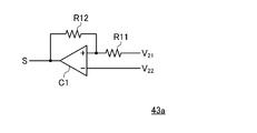
- FIG. 5 is a circuit diagram illustrating a first example of a specific circuit configuration of the comparison unit illustrated in FIG. 2.
- the comparison unit 43a includes a comparator C1 and resistors R11 and R12.
- Resistor R11 has one end connected to one end of first load section 41 and the other end connected to the non-inverting input terminal (+) of comparator C1.
- the resistor R12 has one end connected to the other end of the resistor R11 and the other end connected to the output terminal of the comparator C1.
- the inverting input terminal ( ⁇ ) of the comparator C 1 is connected to one end of the second load unit 42.
- the comparison unit 43a includes one hysteresis comparator (C1, R11, R12).
- the output signal S of the comparison unit 43a is a signal output from the comparator C1, and the signal is low when in a normal state, and is high when in an abnormal state.
- the comparator C1 when the first voltage V 21 and the second voltage V 22 is equal (i.e., normal condition), the comparator C1 outputs a low signal.
- the first voltage V 21 is, if the second voltage V 22 becomes larger than the voltage value obtained by adding a predetermined value (hysteresis) (i.e., an abnormal state), the comparator C1 outputs a high signal.
- comparing unit 43a of the present embodiment can first voltage V 21 and the second voltage V 22 detects the different outputs an output signal S indicating that the abnormal state (high).
- the comparison section 43a of the present embodiment although it is possible to detect the abnormal state when the first voltage V 21 is greater than the second voltage V 22, second voltage V 22 is than the first voltage V 21 An abnormal condition when it becomes large cannot be detected.
- the comparison unit 43a of the present example can detect an abnormal state when at least one of the LED element arrays 221 to 22n constituting the second LED element array group 22 is open due to disconnection or the like, It is not possible to detect an abnormal state when at least one of the LED element arrays 211 to 21m forming the first LED element array group 21 is open due to disconnection or the like.
- the comparison unit 43a tries to detect, for example, an abnormal state when the LED element array is opened, the parallel number m of the LED element arrays 211 to 21m forming the first LED element array group 21 is made as small as possible.
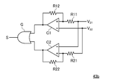
- FIG. 6 is a circuit diagram illustrating a second example of a specific circuit configuration of the comparison unit illustrated in FIG. 2.
- the comparison unit 43b includes comparators C1 and C2, resistors R11, R12, R21, and R22, and an OR circuit G.
- Resistor R11 has one end connected to one end of first load section 41 and the other end connected to the non-inverting input terminal (+) of comparator C1.
- the resistor R12 has one end connected to the other end of the resistor R11 and the other end connected to the output terminal of the comparator C1.
- the inverting input terminal ( ⁇ ) of the comparator C 1 is connected to one end of the second load unit 42.
- the resistor R21 has one end connected to one end of the second load unit 42 and the other end connected to the non-inverting input terminal (+) of the comparator C2.
- One end of the resistor R22 is connected to the other end of the resistor R21, and the other end is connected to the output terminal of the comparator C2.
- the inverting input terminal ( ⁇ ) of the comparator C 2 is connected to one end of the first load unit 41.
- the OR circuit G outputs a logical sum of signals output from the two comparators C1 and C2.
- the comparison unit 43a includes the first hysteresis comparator (C1, R11, R12) and the second hysteresis comparator (C2, R21) whose inputs are opposite to the first hysteresis comparator (C1, R11, R12). , R22) and an OR circuit G that outputs a logical sum of signals output from the first and second hysteresis comparators (C1, R11, R12), (C2, R21, R22).
- the output signal S of the comparison unit 43b is a signal output from the OR circuit G. The signal is low when in a normal state, and is high when in an abnormal state.
- the comparator C1 and the comparator C2 outputs a low signal together.
- the OR circuit G outputs a low signal.
- the first voltage V 21 is, if the second voltage V 22 becomes larger than the voltage value obtained by adding a predetermined value (hysteresis) (abnormal state), the comparator C1 outputs a high signal, the comparator C2 is low Output a signal. In this case, the OR circuit G outputs a high signal.
- the second voltage V 22 is, if larger than the voltage value obtained by adding a predetermined value (hysteresis) to a first voltage V 21 (abnormal state), the comparator C1 outputs a low signal, the comparator C2 is high Output a signal. In this case, the OR circuit G outputs a high signal.
- the comparison unit 43b of the present embodiment although the structure than the comparison section 43a of the first example described above (see FIG. 5) is complicated, the first voltage V 21 is greater than the second voltage V 22 and the abnormal state in the abnormal state when the second voltage V 22 is greater than the first voltage V 21, it is possible to detect both. That is, the comparison unit 43b of this example detects an abnormality in both the LED element arrays 211 to 21m forming the first LED element array group 21 and the LED element arrays 221 to 22n forming the second LED element array group 22. Is possible.
- the comparison unit 43a described above, 43b is only an example, devices capable of a magnitude comparison of the first voltage V 21 and the second voltage V 22 (in particular, the first voltage V 21 and the second voltage V 22 is Any device can be applied to the comparison unit 43 as long as the device can detect a difference.
- the comparison unit 43 is required to output different output signals S depending on whether the first voltage V 21 and the second voltage V 22 are the same or different.
- one of the first voltage V 21 and the second voltage V 22 may be slightly larger than the other even under normal conditions due to the influence of manufacturing variations and noise.
- the comparing unit 43a using a hysteresis comparator, if 43 b, ignoring the slight difference of the first voltage V 21 and the second voltage V 22 as described above
- an output signal S (low) indicating a normal state can be output.
- FIG. 7 is a circuit diagram showing a first example of a specific circuit configuration of the abnormality detection unit.
- FIG. 8 is a circuit diagram illustrating a second example of the specific circuit configuration of the abnormality detection unit.
- the 1st another example of the abnormality detection part shown in FIG. 7 is provided with 41 A of 1st load parts and 42 A of 2nd load parts which were shown in FIG.
- the second example of the abnormality detection unit shown in FIG. 8 includes the first load unit 41B and the second load unit 42B shown in FIG.
- the first abnormality detection unit 4 includes an offset load unit 61A and an offset load unit 62A.
- the abnormality detection unit 4 of the second different example shown in FIG. 8 includes an offset load unit 61B and an offset load unit 62B.
- Various elements having electrical resistance can be applied as the offset load portions 61A, 62A, 61B, 62B.
- the offset load units 61A, 62A, 61B, and 62B are formed of resistors will be exemplified.
- the offset load unit 61A is connected in parallel to the first load unit 41A. Specifically, one end of the offset load unit 61A is connected to one end of the resistor R1, and the other end of the offset load unit 61A is connected to the other end of the resistor R1. Similarly, the offset load unit 62A is connected in parallel to the second load unit 42A. Specifically, one end of the offset load unit 62A is connected to one end of the resistor R2, and the other end of the offset load unit 62A is connected to the other end of the resistor R2.
- the offset load unit 61B is connected in parallel to the first load unit 41B. Specifically, one end of the offset load unit 61B is connected to the collector of the transistor T1, and the other end of the offset load unit 61B is connected to the emitter of the transistor T1. Similarly, the offset load unit 62B is connected in parallel to the second load unit 42B. Specifically, one end of the offset load unit 62B is connected to the collector of the transistor T2, and the other end of the offset load unit 62B is connected to the emitter of the transistor T2.
- one of the first voltage V 21 ′ and the second voltage V 22 ′ in the normal state is set to be larger than the other.
- the size relationship is fixed.
- the comparison unit 43 detects the abnormal state when the magnitude relationship between the first voltage V 21 ′ and the second voltage V 22 ′ is opposite to the magnitude relationship in the normal state.
- the comparison unit 43 can reliably detect the abnormal state by simply comparing the magnitudes of the first voltage V 21 ′ and the second voltage V 22 ′.
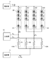
- the LED element rows 211 to 21m and 221 to 22n are connected in parallel, but the arrangement method is arbitrary and is not limited to the arrangement method shown in FIG.
- the LED element rows 211 to 21m and 221 to 22n composed of LEDs 20 arranged in a straight line along the first direction (vertical direction in the figure) are arranged in the second direction perpendicular to the first direction.
- the LEDs 20 are arranged in a planar shape by arranging them in the left-right direction in the figure is illustrated, other LED 20 alignment methods may be adopted.
- FIG. 9 is a block diagram showing another example of the LED alignment method.
- the LED element rows 211 to 21m and 221 to 22n composed of the LEDs 20 arranged linearly along the first direction (vertical direction in the figure) are further arranged along the first direction.
- the LEDs 20 are arranged in a straight line.
- the abnormality detection unit 4 can detect abnormalities in the LED element arrays 211 to 21m and 221 to 22n.
- the LED 20 is arranged in a plane by arranging the LED element rows 211 to 21m and 221 to 22n arranged as shown in FIG. 9 in a second direction (left and right direction in the figure) perpendicular to the first direction. Also good.
- the “number” of resistors R1 and R2 and transistors T1 and T2 having similar characteristics.
- the first load unit 41 and the second load unit 42 are not limited to circuits in which the “number” of elements is adjusted.
- the first load unit 41 and the second load unit 42 may be any one as long as the ratio between the resistance value of the first load unit 41 and the resistance value of the second load unit 42 is n: m. It may be something like this.
- the first load unit 41 and the second load unit 42 may be those in which the “characteristics” (for example, the size of the element) of the elements such as resistors and transistors forming the respective elements are adjusted.
- the first load unit 41 and the second load unit 42 are circuits in which the “number” of elements having similar characteristics is adjusted as shown in FIGS. 3 and 4, the first load unit 41 and the second load unit 42 are simple and accurate. Since the resistance value of the load part 41 and the 2nd load part 42 can be adjusted, it is preferable.
- the lighting device 1 capable of detecting an abnormality in the LED element arrays 211 to 21m and 221 to 22n connected in parallel has been described as an example. If it is an electronic device provided with a row
- the electronic apparatus (illumination device 1) according to the embodiment of the present invention can be grasped as follows, for example.
- the electronic device 1 includes at least one element row 211 to 21m in which at least one element 20 is connected in series, a first element row group 21 in which at least one element row is connected in parallel, and the element rows 221 to 22n.
- a second element array group 22 connected in parallel, a first current I 21 which is the sum of currents flowing through the element arrays 211 to 21m forming the first element array group 21, and the second element array group 22 And the second current I 22 , which is the sum of the currents flowing through the element rows 221 to 22n, satisfying a predetermined relationship, the first element row group 21 and the second element row group 22 And an abnormality detection unit 4 for detecting an abnormality in the element rows 211 to 21m and 221 to 22n, which constitute at least one of them.
- the electronic device 1 includes only the abnormality detection unit 4 that detects that the relationship between the first current I 21 and the second current I 22 is abnormal, and the abnormality of the LED element arrays 211 to 21m and 221 to 22n. Can be detected.
- the abnormality detection unit 4 is connected to the first element array group 21 at one end, and receives the first voltage V 21 that is a voltage corresponding to the first current I 21 from the one end.
- the ratio of the value and the resistance value of the second load unit 42 is Becomes the ratio of the parallel number m of the element rows 211 ⁇ 21m, 221 ⁇ 22n constituting the element array 221 wherein the parallel number n of ⁇ 22n first element array group 21 constituting the element array group 22.
- the abnormality detection unit 4 the magnitude comparison of the first voltage V 21 and the second voltage V 22 (in particular, detects that the first voltage V 21 and the second voltage V 22 are different) only Thus, it is possible to detect an abnormal state. Therefore, the configuration of the abnormality detection unit 4 can be simplified.
- each of the first load part 41A and the second load part 42A is formed by connecting at least one resistor R1, R2 in parallel, and forms the first load part 41A.
- the ratio of the parallel number of the resistor R1 and the parallel number of the resistor R2 forming the second load section 42A is equal to the parallel number m of the element rows 211 to 21m forming the first element row group 21 and the first number. This is a ratio to the parallel number n of the element rows 221 to 22n forming the two-element row group 22.
- the first load portion 41A and the second load portion 42A can be realized by an extremely simple circuit called a parallel connection circuit of resistors R1 and R2.
- each of the first load portion 41B and the second load portion 42B includes at least one transistor T1, T2 in which the one end is the first electrode and the other end is the second electrode.
- the control electrodes of the transistors T1 and T2 constituting the first load portion 41B and the second load portion 42B are connected to each other and at least one constituting the first load portion 41B.
- the control electrode and the first electrode of the two transistors T1 are connected, and the ratio of the parallel number of the transistors T1 forming the first load part 41B and the parallel number of the transistors T2 forming the second load part 42B
- the number m of the element arrays 211 to 21m forming the first element array group 21 and the element arrays 221 to 22n forming the second element array group 22 are the same. It becomes the ratio of the number of parallel n.
- the first load unit 41B and the second load unit 42B are current mirror circuits based on the current flowing through the transistor T1 to which the control electrode and the first electrode are connected. Therefore, in the normal state, the ratio of the first current I 21 and the second current I 22 can be made close to m: n with high accuracy, and each of the first LED element array group 21 and the second LED element array group 22 is obtained. Thus, it is possible to stably supply the same current to the LED element arrays 211 to 21m and 221 to 22n. Furthermore, the first voltage V 21 and the second voltage V 22 can be made equal with high accuracy.
- the first load portion 41B and the second load portion 42B is operated as a current mirror circuit, the first current I 21 and the second current I 22 m: does not lead to up back to n. Therefore, the ratio between the first current I 21 and the second current I 22 deviates from m: n, and the first voltage V 21 and the second voltage V 22 are different. Therefore, the comparison unit 43 can detect an abnormal state.
- the transistor is an NPN bipolar transistor in which the first electrode is a collector, the second electrode is an emitter, and the control electrode is a base.
- offset load portions 61A, 62A, 61B, and 62B connected in parallel to at least one of the first load portions 41A and 41B and the second load portions 42A and 42B. Is further provided.
- the comparison unit 43 detects that the magnitude relationship between the first voltage V 21 ′ and the second voltage V 22 ′ has been reversed using a device that performs a simple magnitude comparison, such as a comparator, so that the normal state It is possible to detect that an abnormal state has occurred.
- the element arrays 211 to 21m and 221 to 22n constituting the first element array group 21 and the second element array group 22 have the same current-voltage characteristics
- the abnormality detection unit 4 is configured such that the ratio of the first current I 21 and the second current I 22 is such that the parallel number m of the element rows 211 to 21m forming the first element row group 21 and the second element row group.
- the element array 221 to 22n forming the number 22 is separated from the parallel number n by more than a predetermined degree, at least one of the first element array group 21 and the second element array group 22 is Abnormalities in the element rows 211 to 21m and 221 to 22n are detected.
- a state in which no current flows uniformly in all the element arrays 211 to 21m and 221 to 22n, that is, the ratio of the first current I 21 and the second current I 22 is a predetermined value from m: n.
- a state that deviates beyond a certain level (for example, a size corresponding to the above-described hysteresis) can be detected as an abnormal state.
- the present invention can be used for an electronic device including a plurality of elements such as LEDs.
- Illumination device 20 LED (element) 21: 1st LED element row group (1st element row group) 211 to 21m: LED element array (element array) 22: 2nd LED element row group (2nd element row group) 221 to 22n: LED element row (element row) 3: Power supply unit 4: Abnormality detection unit 41, 41A, 41B: First load unit 42, 42A, 42B: Second load unit 43, 43a, 43b: Comparison unit 5: Drive control unit 61A, 61B, 62A, 62B: offset load unit I 21: first current I 22: second current V 21: the first voltage V 22: second voltage R1, R2, R11, R12, R21, R22: resistors T1, T2: the transistors C1, C2: Comparator G: OR circuit S: Output signal D: Control signal
Landscapes
- Physics & Mathematics (AREA)
- General Physics & Mathematics (AREA)
- Circuit Arrangement For Electric Light Sources In General (AREA)
- Led Devices (AREA)
- Testing Of Short-Circuits, Discontinuities, Leakage, Or Incorrect Line Connections (AREA)
Abstract
Description
最初に、本発明の実施形態に係る照明装置の全体的な構成例について、図面を参照して説明する。図1は、本発明の実施形態に係る照明装置の全体的な構成例について示すブロック図である。
次に、図1の異常検出部の構成例について、図面を参照して説明する。図2は、図1の異常検出部の構成例について示すブロック図である。
次に、図2に示した異常検出部4の具体的な回路構成例について、図面を参照して説明する。
まず、図2に示した第1負荷部41及び第2負荷部42の具体的な回路構成の第1例について、図面を参照して説明する。図3は、図2に示す第1負荷部及び第2負荷部の具体的な回路構成の第1例について示す回路図である。なお、図示の簡略化のため、図3では、m=1かつn=3の場合を例示している。
また、図2に示した第1負荷部41及び第2負荷部42の具体的な回路構成の第2例について、図面を参照して説明する。図4は、図2に示す第1負荷部及び第2負荷部の具体的な回路構成の第2例について示す回路図である。なお、図示の簡略化のため、図4では、m=1かつn=3の場合を例示している。
次に、図2に示した比較部43の具体的な回路構成の第1例について、図面を参照して説明する。図5は、図2に示す比較部の具体的な回路構成の第1例について示す回路図である。
次に、図2に示した比較部43の具体的な回路構成の第2例について、図面を参照して説明する。図6は、図2に示す比較部の具体的な回路構成の第2例について示す回路図である。
[1] 上述のように、比較部43には、第1電圧V21及び第2電圧V22が等しい場合と異なる場合とにおいて、それぞれ異なる出力信号Sを出力することが求められる。ただし、製造時のばらつきやノイズ等の影響によって、正常状態であっても、第1電圧V21及び第2電圧V22の一方が他方よりも僅かに大きくなることがあり得る。
本発明の実施形態に係る電子機器(照明装置1)は、例えば以下のように把握され得る。
20 : LED(素子)
21 : 第1LED素子列群(第1素子列群)
211~21m : LED素子列(素子列)
22 : 第2LED素子列群(第2素子列群)
221~22n : LED素子列(素子列)
3 : 電源部
4 : 異常検出部
41,41A,41B : 第1負荷部
42,42A,42B : 第2負荷部
43,43a,43b : 比較部
5 : 駆動制御部
61A,61B,62A,62B : オフセット負荷部
I21 : 第1電流
I22 : 第2電流
V21 : 第1電圧
V22 : 第2電圧
R1,R2,R11,R12,R21,R22 : 抵抗器
T1,T2 : トランジスタ
C1,C2 : コンパレータ
G : OR回路
S : 出力信号
D : 制御信号
Claims (7)
- 少なくとも1つの素子が直列接続されて成る素子列が、少なくとも1つ並列接続されて成る第1素子列群と、
前記素子列が、少なくとも1つ並列接続されて成る第2素子列群と、
前記第1素子列群を成す前記素子列を流れる電流の合計である第1電流と、前記第2素子列群を成す前記素子列を流れる電流の合計である第2電流と、が所定の関係を満たすか否かに基づいて、前記第1素子列群及び前記第2素子列群の少なくともいずれか一方を成す前記素子列の異常を検出する異常検出部と、
を備えることを特徴とする電子機器。 - 前記異常検出部が、
一端が前記第1素子列群に接続され、前記第1電流に応じた電圧である第1電圧を当該一端から出力する第1負荷部と、
一端が前記第2素子列群に接続され、前記第2電流に応じた電圧である第2電圧を当該一端から出力する第2負荷部と、
前記第1電圧及び前記第2電圧の大小比較をすることで、前記第1素子列群及び前記第2素子列群の少なくともいずれか一方に属する前記素子列の異常を検出する比較部と、を備え、
前記第1負荷部の他端と前記第2負荷部の他端とが接続され、
前記第1負荷部の抵抗値と前記第2負荷部の抵抗値との比が、前記第2素子列群を成す前記素子列の並列数と前記第1素子列群を成す前記素子列の並列数との比になることを特徴とする請求項1に記載の電子機器。 - 前記第1負荷部及び前記第2負荷部のそれぞれが、抵抗器を少なくとも1つ並列接続したものから成り、
前記第1負荷部を成す前記抵抗器の並列数と前記第2負荷部を成す前記抵抗器の並列数との比が、前記第1素子列群を成す前記素子列の並列数と前記第2素子列群を成す前記素子列の並列数との比になることを特徴とする請求項2に記載の電子機器。 - 前記第1負荷部及び前記第2負荷部のそれぞれが、前記一端が第1電極となり前記他端が第2電極となるトランジスタを少なくとも1つ並列接続したものから成り、
前記第1負荷部及び前記第2負荷部のそれぞれを成す前記トランジスタの制御電極が相互に接続されるとともに、前記第1負荷部を成す少なくとも1つの前記トランジスタの前記制御電極と前記第1電極とが接続され、
前記第1負荷部を成す前記トランジスタの並列数と前記第2負荷部を成す前記トランジスタの並列数との比が、前記第1素子列群を成す前記素子列の並列数と前記第2素子列群を成す前記素子列の並列数との比になることを特徴とする請求項2に記載の電子機器。 - 前記トランジスタが、前記第1電極がコレクタ、前記第2電極がエミッタ、前記制御電極がベースとなるNPN型のバイポーラトランジスタであることを特徴とする請求項4に記載の電子機器。
- 前記第1負荷部及び前記第2負荷部の少なくともいずれか一方に対して並列的に接続されるオフセット負荷部を、
さらに備えることを特徴とする請求項2~5のいずれか1項に記載の電子機器。 - 前記第1素子列群及び前記第2素子列群を成すそれぞれの前記素子列は、電流電圧特性が等しいものであり、
前記異常検出部は、前記第1電流と前記第2電流との比が、前記第1素子列群を成す前記素子列の並列数と前記第2素子列群を成す前記素子列の並列数との比から、所定の程度を超えて乖離した場合に、前記第1素子列群及び前記第2素子列群の少なくともいずれか一方を成す前記素子列の異常を検出することを特徴とする請求項1~6のいずれか1項に記載の電子機器。
Priority Applications (3)
| Application Number | Priority Date | Filing Date | Title |
|---|---|---|---|
| CN201380062962.3A CN104823526B (zh) | 2012-12-27 | 2013-11-27 | 电子设备 |
| US14/758,086 US9970994B2 (en) | 2012-12-27 | 2013-11-27 | Electronic device |
| JP2014554262A JP5961284B2 (ja) | 2012-12-27 | 2013-11-27 | 電子機器 |
Applications Claiming Priority (2)
| Application Number | Priority Date | Filing Date | Title |
|---|---|---|---|
| JP2012283899 | 2012-12-27 | ||
| JP2012-283899 | 2012-12-27 |
Publications (1)
| Publication Number | Publication Date |
|---|---|
| WO2014103598A1 true WO2014103598A1 (ja) | 2014-07-03 |
Family
ID=51020692
Family Applications (1)
| Application Number | Title | Priority Date | Filing Date |
|---|---|---|---|
| PCT/JP2013/081893 Ceased WO2014103598A1 (ja) | 2012-12-27 | 2013-11-27 | 電子機器 |
Country Status (4)
| Country | Link |
|---|---|
| US (1) | US9970994B2 (ja) |
| JP (1) | JP5961284B2 (ja) |
| CN (1) | CN104823526B (ja) |
| WO (1) | WO2014103598A1 (ja) |
Cited By (1)
| Publication number | Priority date | Publication date | Assignee | Title |
|---|---|---|---|---|
| KR20160034792A (ko) | 2014-09-22 | 2016-03-30 | 도시바 라이텍쿠 가부시키가이샤 | 광원장치 |
Families Citing this family (10)
| Publication number | Priority date | Publication date | Assignee | Title |
|---|---|---|---|---|
| CN104062532B (zh) | 2013-03-18 | 2017-03-22 | 戴泺格集成电路(天津)有限公司 | 检测led串中led短路或led串之间匹配性的方法和系统 |
| JP2016212514A (ja) * | 2015-04-30 | 2016-12-15 | 富士通株式会社 | 電源制御装置およびストレージ装置 |
| US9989574B2 (en) * | 2015-05-27 | 2018-06-05 | Infineon Technologies Ag | System and method for short-circuit detection in load chains |
| CN108780981B (zh) * | 2016-03-09 | 2020-06-23 | 株式会社岛津制作所 | 半导体发光装置 |
| TWI654903B (zh) * | 2017-12-21 | 2019-03-21 | 友達光電股份有限公司 | 發光二極體的驅動裝置及其驅動方法 |
| US10849203B2 (en) * | 2018-01-02 | 2020-11-24 | Texas Instruments Incorporated | Multi-string LED current balancing circuit with fault detection |
| CN111065187B (zh) * | 2018-10-17 | 2022-04-26 | 戴洛格半导体(英国)有限公司 | 电流调节器 |
| CN112269139A (zh) * | 2020-10-14 | 2021-01-26 | 无锡友达电子有限公司 | 一种多路led灯故障检测装置 |
| DE102021203550A1 (de) | 2021-04-09 | 2022-10-13 | Siemens Aktiengesellschaft | Beleuchtungsvorrichtung, Notausschalter und Betriebsverfahren |
| DE102023119778A1 (de) * | 2023-07-26 | 2025-01-30 | Ams-Osram International Gmbh | Halbleiterlichtquelle und messverfahren |
Citations (2)
| Publication number | Priority date | Publication date | Assignee | Title |
|---|---|---|---|---|
| JPH07321624A (ja) * | 1994-05-26 | 1995-12-08 | Toshiba Corp | 自己消弧型半導体素子のゲート回路 |
| JP2003317978A (ja) * | 2002-04-19 | 2003-11-07 | Stanley Electric Co Ltd | 車載用led灯具の点灯回路 |
Family Cites Families (15)
| Publication number | Priority date | Publication date | Assignee | Title |
|---|---|---|---|---|
| US374850A (en) * | 1887-12-13 | Method of testing electkic lamp globes | ||
| US2746011A (en) * | 1952-05-21 | 1956-05-15 | Gen Electric | Lamp testing device |
| US20050062481A1 (en) * | 2003-09-19 | 2005-03-24 | Thomas Vaughn | Wayside LED signal for railroad and transit applications |
| US6972570B2 (en) * | 2004-02-11 | 2005-12-06 | Schriefer Jay R | Quick-connect ballast testing and monitoring method and apparatus |
| JP2008108564A (ja) * | 2006-10-25 | 2008-05-08 | Matsushita Electric Works Ltd | Led点灯回路およびそれを用いる照明器具 |
| EP2099262A1 (en) * | 2007-02-26 | 2009-09-09 | Sharp Kabushiki Kaisha | Lamp malfunction detecting device and inverter equipped with the same, back lighting device and display device |
| EP1965609A3 (en) * | 2007-02-27 | 2011-06-15 | Lumination, LLC | LED chain failure detection |
| JP5024789B2 (ja) * | 2007-07-06 | 2012-09-12 | Nltテクノロジー株式会社 | 発光制御回路、発光制御方法、面照明装置及び該面照明装置を備えた液晶表示装置 |
| US8087798B2 (en) * | 2007-11-09 | 2012-01-03 | Lighting Science Group Corporation | Light source with optimized electrical, optical, and economical performance |
| WO2010022350A2 (en) * | 2008-08-21 | 2010-02-25 | Asic Advantage Inc. | Light emitting diode fault monitoring |
| JP2010123273A (ja) | 2008-11-17 | 2010-06-03 | Ccs Inc | Led照明装置 |
| US8860427B2 (en) * | 2009-04-20 | 2014-10-14 | Infineon Technologies Ag | Failure detection for series of electrical loads |
| EP2487998A1 (en) * | 2011-02-09 | 2012-08-15 | National Semiconductor Corporation | Technique for identifying at least one faulty light emitting diode in a string of light emitting diodes |
| EP2487999A1 (en) * | 2011-02-09 | 2012-08-15 | National Semiconductor Corporation | Technique for identifying at least one faulty light emitting diode in multiple strings of light emitting diodes |
| JP5942314B2 (ja) * | 2011-02-22 | 2016-06-29 | パナソニックIpマネジメント株式会社 | 点灯装置および、これを用いた照明器具 |
-
2013
- 2013-11-27 JP JP2014554262A patent/JP5961284B2/ja not_active Expired - Fee Related
- 2013-11-27 CN CN201380062962.3A patent/CN104823526B/zh not_active Expired - Fee Related
- 2013-11-27 WO PCT/JP2013/081893 patent/WO2014103598A1/ja not_active Ceased
- 2013-11-27 US US14/758,086 patent/US9970994B2/en not_active Expired - Fee Related
Patent Citations (2)
| Publication number | Priority date | Publication date | Assignee | Title |
|---|---|---|---|---|
| JPH07321624A (ja) * | 1994-05-26 | 1995-12-08 | Toshiba Corp | 自己消弧型半導体素子のゲート回路 |
| JP2003317978A (ja) * | 2002-04-19 | 2003-11-07 | Stanley Electric Co Ltd | 車載用led灯具の点灯回路 |
Cited By (1)
| Publication number | Priority date | Publication date | Assignee | Title |
|---|---|---|---|---|
| KR20160034792A (ko) | 2014-09-22 | 2016-03-30 | 도시바 라이텍쿠 가부시키가이샤 | 광원장치 |
Also Published As
| Publication number | Publication date |
|---|---|
| JPWO2014103598A1 (ja) | 2017-01-12 |
| CN104823526A (zh) | 2015-08-05 |
| CN104823526B (zh) | 2016-08-24 |
| US20150355289A1 (en) | 2015-12-10 |
| US9970994B2 (en) | 2018-05-15 |
| JP5961284B2 (ja) | 2016-08-02 |
Similar Documents
| Publication | Publication Date | Title |
|---|---|---|
| JP5961284B2 (ja) | 電子機器 | |
| US8247993B2 (en) | Apparatus for driving multi-light emitting devices | |
| US8829884B2 (en) | Current balancing circuit and method | |
| KR102113388B1 (ko) | Led 고장 검출 장치 | |
| US10085333B1 (en) | LED failure detecting device | |
| US9107262B2 (en) | Illumination apparatus including semiconductor light emitting diodes | |
| WO2019235027A1 (ja) | 組電池監視システム | |
| CN103348775A (zh) | 识别led串中的故障的方法 | |
| JP2011171547A (ja) | 発光ダイオードの故障検出回路 | |
| EP2923530B1 (en) | Current mirror circuit and method | |
| US8896319B2 (en) | Light emitting device control circuit and short detection circuit thereof | |
| US20150097573A1 (en) | Load apparatus for testing | |
| JP5426255B2 (ja) | 光源制御回路、光源制御方法、光源装置 | |
| CN109845403B (zh) | 特别是用于车辆的led照明装置 | |
| US9360949B2 (en) | Human interface device | |
| KR102548753B1 (ko) | Led 스트링들의 전류 밸런싱을 위한 led 구동 회로 | |
| US20060082541A1 (en) | Input detection device and related method | |
| JP5976565B2 (ja) | 電子部品検査装置 | |
| US11920990B2 (en) | In-vehicle temperature detection circuit | |
| CN102647824A (zh) | Led驱动电路的输出电流分段补偿电路 | |
| Choi | Adaptive current-mirror LED driver employing super-diode configuration | |
| JP2015125802A (ja) | 照明装置 | |
| JP5947031B2 (ja) | 順方向電圧測定装置 | |
| JP2013021135A (ja) | 発光素子駆動回路および発光素子異常検出方法 | |
| CN101425248A (zh) | 面板与主机板间之双线接口 |
Legal Events
| Date | Code | Title | Description |
|---|---|---|---|
| 121 | Ep: the epo has been informed by wipo that ep was designated in this application |
Ref document number: 13867668 Country of ref document: EP Kind code of ref document: A1 |
|
| ENP | Entry into the national phase |
Ref document number: 2014554262 Country of ref document: JP Kind code of ref document: A |
|
| WWE | Wipo information: entry into national phase |
Ref document number: 14758086 Country of ref document: US |
|
| NENP | Non-entry into the national phase |
Ref country code: DE |
|
| 122 | Ep: pct application non-entry in european phase |
Ref document number: 13867668 Country of ref document: EP Kind code of ref document: A1 |