WO2014103265A1 - Power amplifier - Google Patents
Power amplifier Download PDFInfo
- Publication number
- WO2014103265A1 WO2014103265A1 PCT/JP2013/007492 JP2013007492W WO2014103265A1 WO 2014103265 A1 WO2014103265 A1 WO 2014103265A1 JP 2013007492 W JP2013007492 W JP 2013007492W WO 2014103265 A1 WO2014103265 A1 WO 2014103265A1
- Authority
- WO
- WIPO (PCT)
- Prior art keywords
- current
- group
- power amplifier
- switches
- current sources
- Prior art date
Links
Images


Classifications
-
- H—ELECTRICITY
- H03—ELECTRONIC CIRCUITRY
- H03F—AMPLIFIERS
- H03F3/00—Amplifiers with only discharge tubes or only semiconductor devices as amplifying elements
- H03F3/20—Power amplifiers, e.g. Class B amplifiers, Class C amplifiers
- H03F3/21—Power amplifiers, e.g. Class B amplifiers, Class C amplifiers with semiconductor devices only
- H03F3/211—Power amplifiers, e.g. Class B amplifiers, Class C amplifiers with semiconductor devices only using a combination of several amplifiers
-
- H—ELECTRICITY
- H03—ELECTRONIC CIRCUITRY
- H03F—AMPLIFIERS
- H03F3/00—Amplifiers with only discharge tubes or only semiconductor devices as amplifying elements
- H03F3/20—Power amplifiers, e.g. Class B amplifiers, Class C amplifiers
- H03F3/21—Power amplifiers, e.g. Class B amplifiers, Class C amplifiers with semiconductor devices only
- H03F3/217—Class D power amplifiers; Switching amplifiers
- H03F3/2178—Class D power amplifiers; Switching amplifiers using more than one switch or switching amplifier in parallel or in series
-
- H—ELECTRICITY
- H03—ELECTRONIC CIRCUITRY
- H03F—AMPLIFIERS
- H03F3/00—Amplifiers with only discharge tubes or only semiconductor devices as amplifying elements
- H03F3/20—Power amplifiers, e.g. Class B amplifiers, Class C amplifiers
- H03F3/24—Power amplifiers, e.g. Class B amplifiers, Class C amplifiers of transmitter output stages
- H03F3/245—Power amplifiers, e.g. Class B amplifiers, Class C amplifiers of transmitter output stages with semiconductor devices only
-
- H—ELECTRICITY
- H03—ELECTRONIC CIRCUITRY
- H03F—AMPLIFIERS
- H03F2200/00—Indexing scheme relating to amplifiers
- H03F2200/18—Indexing scheme relating to amplifiers the bias of the gate of a FET being controlled by a control signal
-
- H—ELECTRICITY
- H03—ELECTRONIC CIRCUITRY
- H03F—AMPLIFIERS
- H03F2200/00—Indexing scheme relating to amplifiers
- H03F2200/432—Two or more amplifiers of different type are coupled in parallel at the input or output, e.g. a class D and a linear amplifier, a class B and a class A amplifier
-
- H—ELECTRICITY
- H03—ELECTRONIC CIRCUITRY
- H03F—AMPLIFIERS
- H03F2203/00—Indexing scheme relating to amplifiers with only discharge tubes or only semiconductor devices as amplifying elements covered by H03F3/00
- H03F2203/20—Indexing scheme relating to power amplifiers, e.g. Class B amplifiers, Class C amplifiers
- H03F2203/21—Indexing scheme relating to power amplifiers, e.g. Class B amplifiers, Class C amplifiers with semiconductor devices only
- H03F2203/211—Indexing scheme relating to power amplifiers, e.g. Class B amplifiers, Class C amplifiers with semiconductor devices only using a combination of several amplifiers
- H03F2203/21109—An input signal being distributed by switching to a plurality of paralleled power amplifiers
-
- H—ELECTRICITY
- H03—ELECTRONIC CIRCUITRY
- H03F—AMPLIFIERS
- H03F2203/00—Indexing scheme relating to amplifiers with only discharge tubes or only semiconductor devices as amplifying elements covered by H03F3/00
- H03F2203/20—Indexing scheme relating to power amplifiers, e.g. Class B amplifiers, Class C amplifiers
- H03F2203/21—Indexing scheme relating to power amplifiers, e.g. Class B amplifiers, Class C amplifiers with semiconductor devices only
- H03F2203/211—Indexing scheme relating to power amplifiers, e.g. Class B amplifiers, Class C amplifiers with semiconductor devices only using a combination of several amplifiers
- H03F2203/21136—An input signal of a power amplifier being on/off switched
-
- H—ELECTRICITY
- H03—ELECTRONIC CIRCUITRY
- H03F—AMPLIFIERS
- H03F2203/00—Indexing scheme relating to amplifiers with only discharge tubes or only semiconductor devices as amplifying elements covered by H03F3/00
- H03F2203/20—Indexing scheme relating to power amplifiers, e.g. Class B amplifiers, Class C amplifiers
- H03F2203/21—Indexing scheme relating to power amplifiers, e.g. Class B amplifiers, Class C amplifiers with semiconductor devices only
- H03F2203/211—Indexing scheme relating to power amplifiers, e.g. Class B amplifiers, Class C amplifiers with semiconductor devices only using a combination of several amplifiers
- H03F2203/21145—Output signals are combined by switching a plurality of paralleled power amplifiers to a common output
-
- H—ELECTRICITY
- H03—ELECTRONIC CIRCUITRY
- H03F—AMPLIFIERS
- H03F2203/00—Indexing scheme relating to amplifiers with only discharge tubes or only semiconductor devices as amplifying elements covered by H03F3/00
- H03F2203/20—Indexing scheme relating to power amplifiers, e.g. Class B amplifiers, Class C amplifiers
- H03F2203/21—Indexing scheme relating to power amplifiers, e.g. Class B amplifiers, Class C amplifiers with semiconductor devices only
- H03F2203/211—Indexing scheme relating to power amplifiers, e.g. Class B amplifiers, Class C amplifiers with semiconductor devices only using a combination of several amplifiers
- H03F2203/21184—Indexing scheme relating to power amplifiers, e.g. Class B amplifiers, Class C amplifiers with semiconductor devices only using a combination of several amplifiers the supply current of a power amplifier being continuously measured, e.g. by a resistor, a current mirror, to produce a controlling signal
-
- H—ELECTRICITY
- H03—ELECTRONIC CIRCUITRY
- H03F—AMPLIFIERS
- H03F3/00—Amplifiers with only discharge tubes or only semiconductor devices as amplifying elements
- H03F3/04—Amplifiers with only discharge tubes or only semiconductor devices as amplifying elements with semiconductor devices only
-
- H—ELECTRICITY
- H03—ELECTRONIC CIRCUITRY
- H03F—AMPLIFIERS
- H03F3/00—Amplifiers with only discharge tubes or only semiconductor devices as amplifying elements
- H03F3/34—Dc amplifiers in which all stages are dc-coupled
- H03F3/343—Dc amplifiers in which all stages are dc-coupled with semiconductor devices only
- H03F3/345—Dc amplifiers in which all stages are dc-coupled with semiconductor devices only with field-effect devices
Abstract
Description
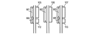
図1は、本発明の実施の形態1における電力増幅器の構成図である。 (Embodiment 1)
FIG. 1 is a configuration diagram of a power amplifier according to
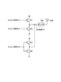
図6は、本発明の実施の形態2の電力増幅器の構成図である。図6において、図1と同様の構成要素については同じ符号を用い、説明を省略する。 (Embodiment 2)
FIG. 6 is a configuration diagram of the power amplifier according to the second embodiment of the present invention. In FIG. 6, the same components as those in FIG.
タイミング信号Dの位相=タイミング信号Eの位相+45度=タイミング信号Fの位相+90度
タイミング信号Aの位相=タイミング信号Dの位相+180度
タイミング信号Bの位相=タイミング信号Eの位相+180度
タイミング信号Cの位相=タイミング信号Fの位相+180度 Timing signal A phase = timing signal B phase + 45 degrees = timing signal C phase + 90 degrees Timing signal D phase = timing signal E phase + 45 degrees = timing signal F phase + 90 degrees Timing signal A phase = timing signal D phase + 180 degrees Timing signal B phase = timing signal E phase + 180 degrees Timing signal C phase = timing signal F phase + 180 degrees
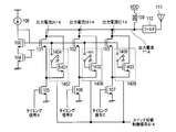
図8は、本発明の実施の形態3の電力増幅器の構成図である。図8において、図1と同様の構成要素については同じ符号を用い、説明を省略する。 (Embodiment 3)
FIG. 8 is a configuration diagram of the power amplifier according to the third embodiment of the present invention. In FIG. 8, the same components as those in FIG.
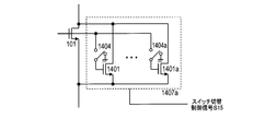
図14は、本発明の実施の形態4の電力増幅器の構成図である。図14において、図1と同様の構成要素については同じ符号を用い、説明を省略する。 (Embodiment 4)
FIG. 14 is a configuration diagram of the power amplifier according to the fourth embodiment of the present invention. In FIG. 14, the same components as those in FIG.
105、106、107、405、406、407 NMOSトランジスタ(スイッチ)
108 基準電流源
109 コイル
110 帯域通過フィルタ
111 アンテナ
112、113 負荷調整用MOSトランジスタ
114 タイミング信号生成部
120 非反転部(第1グループ)
301、302、303 電流源
304、305、306 スイッチ
420 バラン
430 反転部(第2グループ)
612、613 NMOSトランジスタ(高調波抑制用電流源)
614、615 NMOSトランジスタ(高調波抑制用スイッチ)
1401、1402、1403 NMOSトランジスタ
1404、1405、1406 スイッチ
1407、1408、1409 微調整回路
A、B、C、D、E、F タイミング信号
G、H、K タイミング信号(高調波抑制用タイミング信号) 100, 101, 102, 103, 401, 402, 403 NMOS transistor (current source, current mirror circuit)
105, 106, 107, 405, 406, 407 NMOS transistor (switch)
108 Reference
301, 302, 303
612, 613 NMOS transistor (current source for suppressing harmonics)
614, 615 NMOS transistor (harmonic suppression switch)
1401, 1402, 1403
Claims (12)
- 所定電流を流すn個(nは3以上の自然数)の電流源と、
前記n個の電流源の電流経路をそれぞれ開閉するn個のスイッチと、
前記n個のスイッチをそれぞれオン/オフするn個のタイミング信号を生成する信号生成部と、
を具備し、
前記n個のタイミング信号は、デューティー比が互いに同一、且つ、位相が互いに異なる信号であり、
前記n個の電流源に流れる電流に基づき電力増幅された信号を出力する電力増幅器。 N current sources (n is a natural number of 3 or more) for supplying a predetermined current;
N switches for respectively opening and closing current paths of the n current sources;
A signal generator for generating n timing signals for turning on / off each of the n switches;
Comprising
The n timing signals are signals having the same duty ratio and different phases.
A power amplifier that outputs a signal amplified based on a current flowing through the n current sources. - 前記n個の電流源は、
基準電流を流す基準電流源と、
前記基準電流を転写するn個のカレントミラー回路と、
を具備する、
請求項1記載の電力増幅器。 The n current sources are:
A reference current source for supplying a reference current;
N current mirror circuits for transferring the reference current;
Comprising
The power amplifier according to claim 1. - 前記n個のスイッチは、n個のMOSトランジスタである、
請求項1記載の電力増幅器。 The n switches are n MOS transistors.
The power amplifier according to claim 1. - 前記nは3であり、
前記n個のタイミング信号は、0度、45度、90度に位相がそれぞれずれた信号である、
請求項1記載の電力増幅器。 N is 3;
The n timing signals are signals whose phases are shifted to 0 degrees, 45 degrees, and 90 degrees, respectively.
The power amplifier according to claim 1. - 前記nは3であり、
前記n個の電流源の電流値の比は、1:21/2:1である、
請求項1記載の電力増幅器。 N is 3;
The ratio of the current values of the n current sources is 1: 2 1/2 : 1.
The power amplifier according to claim 1. - 前記n個のスイッチである前記n個のMOSトランジスタは、チャネル長Lが一定で、且つ、チャネル幅Wが、対応する前記n個の電流源の電流値にそれぞれ比例したサイズである、
請求項3記載の電力増幅器。 The n MOS transistors that are the n switches have a constant channel length L and a channel width W that is proportional to the current value of the corresponding n current sources.
The power amplifier according to claim 3. - 前記n個のMOSトランジスタのうち、他よりサイズが小さな1つまたは複数のMOSトランジスタとゲート端子がそれぞれ結合される1つまたは複数の負荷調整用MOSトランジスタを具備し、
前記1つまたは複数の負荷調整用MOSトランジスタは、ドレインおよびソースが前記ドレインおよび前記ソース間に電流を流さない接続とされ、
前記n個のMOSトランジスタのゲート端子の負荷が、前記負荷調整用MOSトランジスタのゲート負荷の加算により、ほぼ同一にされている、
請求項6記載の電力増幅器。 Among the n MOS transistors, one or more MOS transistors having a smaller size than the other and one or more load adjusting MOS transistors each having a gate terminal coupled thereto,
In the one or more load adjusting MOS transistors, a drain and a source are connected so that no current flows between the drain and the source,
The load at the gate terminal of the n MOS transistors is made substantially the same by adding the gate load of the load adjusting MOS transistor.
The power amplifier according to claim 6. - 前記n個は6以上の偶数であり、
前記n個の電流源、前記n個のスイッチ、および、前記n個のタイミング信号を、半分の第1グループと、残り半分の第2グループとに分類した場合、
前記第1グループと前記第2グループとが逆位相で動作し、
前記第1グループのn/2個の電流源を流れる合算電流と、前記第2グループのn/2個の電流源を流れる合算電流との差分により電力増幅された信号を出力する、
請求項1記載の電力増幅器。 N is an even number of 6 or more;
When the n current sources, the n switches, and the n timing signals are classified into a half first group and a remaining half second group,
The first group and the second group operate in opposite phases;
Outputting a signal amplified by the difference between the total current flowing through the n / 2 current sources of the first group and the total current flowing through the n / 2 current sources of the second group;
The power amplifier according to claim 1. - 前記n個の電流源は、第1グループの3個の電流源、および、第2グループの3個の電流源からなり、
前記n個のスイッチは、前記第1グループの3個の電流源に対応する第1グループの3個のスイッチ、および、前記第2グループの3個の電流源に対応する第2グループの3個のスイッチからなり、
前記n個のタイミング信号は、前記第1グループの3個のスイッチに対応する第1グループの3個のタイミング信号、および、前記第2グループの3個のスイッチに対応する第2グループの3個のタイミング信号からなり、
前記第1グループの3個の電流源の電流値の比は、1:21/2:1であり、
前記第2グループの3個の電流源の電流値の比は、1:21/2:1であり、
前記第1グループの3個のタイミング信号は、0度、45度、90度に位相がそれぞれずれた信号であり、
前記第2グループの3個のタイミング信号は、180度、225度、270度に位相がそれぞれずれた信号であり、
前記第1グループの3個の電流源を流れる合算電流と、前記第2グループの3個の電流源を流れる合算電流との差分により電力増幅された信号を出力する、
請求項1記載の電力増幅器。 The n current sources include three current sources in a first group and three current sources in a second group,
The n switches include three switches of the first group corresponding to the three current sources of the first group and three switches of the second group corresponding to the three current sources of the second group. Consisting of
The n timing signals include three timing signals of the first group corresponding to the three switches of the first group and three of the second group corresponding to the three switches of the second group. Timing signal,
The ratio of the current values of the three current sources of the first group is 1: 2 1/2 : 1
The ratio of the current values of the three current sources of the second group is 1: 2 1/2 : 1
The three timing signals of the first group are signals whose phases are shifted to 0 degrees, 45 degrees, and 90 degrees, respectively.
The three timing signals of the second group are signals whose phases are shifted by 180 degrees, 225 degrees, and 270 degrees, respectively.
Outputting a signal amplified by the difference between the total current flowing through the three current sources of the first group and the total current flowing through the three current sources of the second group;
The power amplifier according to claim 1. - 所定電流を流す高調波抑制用電流源と、
前記高調波抑制用電流源の電流経路を開閉する高調波抑制用スイッチと、
前記高調波抑制用スイッチをオン/オフする高調波抑制用タイミング信号を生成する信号生成部と、
前記高調波抑制用タイミング信号は、前記タイミング信号より周波数が2倍であり、
前記高調波抑制用電流源の電流が出力に加算される、
請求項1記載の電力増幅器。 A current source for suppressing harmonics to flow a predetermined current;
A harmonic suppression switch that opens and closes a current path of the harmonic suppression current source;
A signal generator for generating a harmonic suppression timing signal for turning on / off the harmonic suppression switch;
The harmonic suppression timing signal has a frequency twice that of the timing signal,
The current of the harmonic suppression current source is added to the output,
The power amplifier according to claim 1. - 前記高調波抑制用タイミング信号の位相は、前記電力増幅された信号に含まれる高調波を抑制する位相に設定されている、
請求項10記載の電力増幅器。 The phase of the harmonic suppression timing signal is set to a phase that suppresses harmonics included in the power amplified signal.
The power amplifier according to claim 10. - 前記複数の高調波抑制用電流源および前記複数の高調波抑制用スイッチのうち動作させる個数を選択的に切り替え可能な個数切替手段と、
を具備する請求項10に記載の電流増幅器。
A number switching means capable of selectively switching the number to be operated among the plurality of harmonic suppression current sources and the plurality of harmonic suppression switches;
The current amplifier according to claim 10.
Priority Applications (2)
| Application Number | Priority Date | Filing Date | Title |
|---|---|---|---|
| JP2014554129A JP6496550B2 (en) | 2012-12-25 | 2013-12-19 | Power amplifier |
| US14/379,651 US9490758B2 (en) | 2012-12-25 | 2013-12-19 | Power amplifier |
Applications Claiming Priority (2)
| Application Number | Priority Date | Filing Date | Title |
|---|---|---|---|
| JP2012280974 | 2012-12-25 | ||
| JP2012-280974 | 2012-12-25 |
Publications (1)
| Publication Number | Publication Date |
|---|---|
| WO2014103265A1 true WO2014103265A1 (en) | 2014-07-03 |
Family
ID=51020385
Family Applications (1)
| Application Number | Title | Priority Date | Filing Date |
|---|---|---|---|
| PCT/JP2013/007492 WO2014103265A1 (en) | 2012-12-25 | 2013-12-19 | Power amplifier |
Country Status (3)
| Country | Link |
|---|---|
| US (1) | US9490758B2 (en) |
| JP (1) | JP6496550B2 (en) |
| WO (1) | WO2014103265A1 (en) |
Cited By (3)
| Publication number | Priority date | Publication date | Assignee | Title |
|---|---|---|---|---|
| JP2017028661A (en) * | 2015-07-28 | 2017-02-02 | 日本電信電話株式会社 | Wireless oscillation circuit and wireless terminal |
| US11025211B2 (en) | 2019-03-14 | 2021-06-01 | Kabushiki Kaisha Toshiba | Amplification apparatus and transmission apparatus |
| US11139782B2 (en) | 2019-03-13 | 2021-10-05 | Kabushiki Kaisha Toshiba | Amplification apparatus and transmission apparatus |
Families Citing this family (2)
| Publication number | Priority date | Publication date | Assignee | Title |
|---|---|---|---|---|
| KR102155371B1 (en) * | 2013-09-09 | 2020-09-11 | 삼성전자주식회사 | Method and apparatus of wireless power transmission for cancelling harmonics noise |
| EP3667913A1 (en) | 2018-12-13 | 2020-06-17 | Stichting IMEC Nederland | Amplitude sweep generator and method |
Citations (8)
| Publication number | Priority date | Publication date | Assignee | Title |
|---|---|---|---|---|
| JPH04256882A (en) * | 1991-02-08 | 1992-09-11 | Furuno Electric Co Ltd | Sending pulse generation circuit in pulse radar |
| JP2000323966A (en) * | 1998-09-11 | 2000-11-24 | Advantest Corp | Waveform generator, semiconductor testing device and semiconductor device |
| US20020180547A1 (en) * | 2001-05-23 | 2002-12-05 | Staszewski Robert B. | Efficient pulse amplitude modulation transmit modulation |
| JP2003143023A (en) * | 2001-11-05 | 2003-05-16 | Nec Corp | Transmitter |
| JP2004363887A (en) * | 2003-06-04 | 2004-12-24 | Casio Comput Co Ltd | Current generating/supplying circuit |
| JP2011041105A (en) * | 2009-08-14 | 2011-02-24 | Semiconductor Technology Academic Research Center | High-frequency signal generator circuit |
| JP2011234348A (en) * | 2010-04-29 | 2011-11-17 | Mediatek Singapore Pte Ltd | Integrated circuit, communication unit and method for improved amplitude resolution of rf-dac |
| JP2012069616A (en) * | 2010-09-22 | 2012-04-05 | Casio Comput Co Ltd | Current mirror circuit, current generation circuit, and light emitting device |
Family Cites Families (13)
| Publication number | Priority date | Publication date | Assignee | Title |
|---|---|---|---|---|
| JP3039791B2 (en) * | 1990-06-08 | 2000-05-08 | 富士通株式会社 | DA converter |
| JP3499813B2 (en) * | 2000-08-29 | 2004-02-23 | Necマイクロシステム株式会社 | Current cell type digital / analog converter |
| JP2002094378A (en) * | 2000-09-13 | 2002-03-29 | Fujitsu Ltd | Digital to analog converter |
| KR100742063B1 (en) | 2003-05-26 | 2007-07-23 | 가시오게산키 가부시키가이샤 | Electric current generation supply circuit and display device |
| US7532065B2 (en) * | 2005-07-12 | 2009-05-12 | Agere Systems Inc. | Analog amplifier having DC offset cancellation circuit and method of offset cancellation for analog amplifiers |
| JPWO2007043122A1 (en) * | 2005-09-30 | 2009-04-16 | 富士通株式会社 | Variable gain amplifier and control method thereof |
| EP2063531A4 (en) | 2006-09-14 | 2015-07-22 | Nec Corp | Amplifying unit, method of output control and control program |
| US7924096B2 (en) * | 2009-03-06 | 2011-04-12 | Analog Devices, Inc. | Input buffer with impedance cancellation |
| ES2381533T3 (en) * | 2009-05-12 | 2012-05-29 | St-Ericsson Sa | RF amplifier with digital filter for polar transmitter |
| KR20100129575A (en) * | 2009-06-01 | 2010-12-09 | 삼성전자주식회사 | Noninverting amplifier and voltage supply circuit having its |
| JP2012023431A (en) * | 2010-07-12 | 2012-02-02 | Renesas Electronics Corp | Sine wave generating circuit |
| KR101419806B1 (en) * | 2010-11-19 | 2014-07-17 | 한국전자통신연구원 | Variable gain amplifier with fixed bandwidth |
| US8525586B2 (en) * | 2011-08-15 | 2013-09-03 | Mediatek Inc. | Gain stage with DC offset compensation and method thereof |
-
2013
- 2013-12-19 JP JP2014554129A patent/JP6496550B2/en not_active Expired - Fee Related
- 2013-12-19 US US14/379,651 patent/US9490758B2/en not_active Expired - Fee Related
- 2013-12-19 WO PCT/JP2013/007492 patent/WO2014103265A1/en active Application Filing
Patent Citations (8)
| Publication number | Priority date | Publication date | Assignee | Title |
|---|---|---|---|---|
| JPH04256882A (en) * | 1991-02-08 | 1992-09-11 | Furuno Electric Co Ltd | Sending pulse generation circuit in pulse radar |
| JP2000323966A (en) * | 1998-09-11 | 2000-11-24 | Advantest Corp | Waveform generator, semiconductor testing device and semiconductor device |
| US20020180547A1 (en) * | 2001-05-23 | 2002-12-05 | Staszewski Robert B. | Efficient pulse amplitude modulation transmit modulation |
| JP2003143023A (en) * | 2001-11-05 | 2003-05-16 | Nec Corp | Transmitter |
| JP2004363887A (en) * | 2003-06-04 | 2004-12-24 | Casio Comput Co Ltd | Current generating/supplying circuit |
| JP2011041105A (en) * | 2009-08-14 | 2011-02-24 | Semiconductor Technology Academic Research Center | High-frequency signal generator circuit |
| JP2011234348A (en) * | 2010-04-29 | 2011-11-17 | Mediatek Singapore Pte Ltd | Integrated circuit, communication unit and method for improved amplitude resolution of rf-dac |
| JP2012069616A (en) * | 2010-09-22 | 2012-04-05 | Casio Comput Co Ltd | Current mirror circuit, current generation circuit, and light emitting device |
Cited By (3)
| Publication number | Priority date | Publication date | Assignee | Title |
|---|---|---|---|---|
| JP2017028661A (en) * | 2015-07-28 | 2017-02-02 | 日本電信電話株式会社 | Wireless oscillation circuit and wireless terminal |
| US11139782B2 (en) | 2019-03-13 | 2021-10-05 | Kabushiki Kaisha Toshiba | Amplification apparatus and transmission apparatus |
| US11025211B2 (en) | 2019-03-14 | 2021-06-01 | Kabushiki Kaisha Toshiba | Amplification apparatus and transmission apparatus |
Also Published As
| Publication number | Publication date |
|---|---|
| US20150015338A1 (en) | 2015-01-15 |
| JP6496550B2 (en) | 2019-04-03 |
| JPWO2014103265A1 (en) | 2017-01-12 |
| US9490758B2 (en) | 2016-11-08 |
Similar Documents
| Publication | Publication Date | Title |
|---|---|---|
| JP6496550B2 (en) | Power amplifier | |
| US9641141B1 (en) | Harmonics suppression circuit for a switch-mode power amplifier | |
| US8749275B2 (en) | Differential circuit | |
| EP2251977A2 (en) | Low-noise, low-power, low drift offset correction in operational and instrumentation amplifiers | |
| US20190158075A1 (en) | Harmonic multiplier architecture | |
| US8896358B2 (en) | Phase interpolator having adaptively biased phase mixer | |
| US20140104088A1 (en) | Differential switch drive circuit and current steering digital-to-analog converter | |
| US9148089B2 (en) | Transmitting apparatus and transmission method | |
| TW201541857A (en) | A dead time circuit for a switching circuit and a switching amplifier | |
| US20080122536A1 (en) | Three-stage amplifier | |
| JP2014199966A (en) | Polarity switching amplifier circuit | |
| JP5778688B2 (en) | High voltage inversion type charge pump | |
| JP6240081B2 (en) | amplifier | |
| US20140009139A1 (en) | Differential current source and differential current mirror circuit | |
| US8111181B2 (en) | Single-ended polar transmitting circuit with current salvaging and substantially constant bandwidth | |
| US8543078B2 (en) | Harmonic mixer circuit | |
| JP6254014B2 (en) | Harmonic rejection power amplifier | |
| JP2012015961A (en) | Frequency conversion circuit, signal processing circuit, and receiver | |
| KR101646471B1 (en) | Active balun device | |
| US11683015B2 (en) | Class-D amplifier with deadtime distortion compensation | |
| JP4520177B2 (en) | Signal processing circuit | |
| JP5592334B2 (en) | Splitter circuit | |
| US11387786B2 (en) | Amplifier | |
| JP7367774B2 (en) | driver circuit | |
| KR101004902B1 (en) | Active balun with stack structure |
Legal Events
| Date | Code | Title | Description |
|---|---|---|---|
| ENP | Entry into the national phase |
Ref document number: 2014554129 Country of ref document: JP Kind code of ref document: A |
|
| WWE | Wipo information: entry into national phase |
Ref document number: 14379651 Country of ref document: US |
|
| 121 | Ep: the epo has been informed by wipo that ep was designated in this application |
Ref document number: 13869403 Country of ref document: EP Kind code of ref document: A1 |
|
| NENP | Non-entry into the national phase |
Ref country code: DE |
|
| 122 | Ep: pct application non-entry in european phase |
Ref document number: 13869403 Country of ref document: EP Kind code of ref document: A1 |