WO2014097904A1 - 照明装置 - Google Patents
照明装置 Download PDFInfo
- Publication number
- WO2014097904A1 WO2014097904A1 PCT/JP2013/082839 JP2013082839W WO2014097904A1 WO 2014097904 A1 WO2014097904 A1 WO 2014097904A1 JP 2013082839 W JP2013082839 W JP 2013082839W WO 2014097904 A1 WO2014097904 A1 WO 2014097904A1
- Authority
- WO
- WIPO (PCT)
- Prior art keywords
- light emitting
- emitting elements
- current
- adjustment circuit
- amount
- Prior art date
- Legal status (The legal status is an assumption and is not a legal conclusion. Google has not performed a legal analysis and makes no representation as to the accuracy of the status listed.)
- Ceased
Links
Images

Classifications
-
- H—ELECTRICITY
- H05—ELECTRIC TECHNIQUES NOT OTHERWISE PROVIDED FOR
- H05B—ELECTRIC HEATING; ELECTRIC LIGHT SOURCES NOT OTHERWISE PROVIDED FOR; CIRCUIT ARRANGEMENTS FOR ELECTRIC LIGHT SOURCES, IN GENERAL
- H05B45/00—Circuit arrangements for operating light-emitting diodes [LED]
- H05B45/40—Details of LED load circuits
- H05B45/44—Details of LED load circuits with an active control inside an LED matrix
- H05B45/48—Details of LED load circuits with an active control inside an LED matrix having LEDs organised in strings and incorporating parallel shunting devices
-
- H—ELECTRICITY
- H10—SEMICONDUCTOR DEVICES; ELECTRIC SOLID-STATE DEVICES NOT OTHERWISE PROVIDED FOR
- H10K—ORGANIC ELECTRIC SOLID-STATE DEVICES
- H10K50/00—Organic light-emitting devices
- H10K50/10—OLEDs or polymer light-emitting diodes [PLED]
- H10K50/11—OLEDs or polymer light-emitting diodes [PLED] characterised by the electroluminescent [EL] layers
- H10K50/125—OLEDs or polymer light-emitting diodes [PLED] characterised by the electroluminescent [EL] layers specially adapted for multicolour light emission, e.g. for emitting white light
- H10K50/13—OLEDs or polymer light-emitting diodes [PLED] characterised by the electroluminescent [EL] layers specially adapted for multicolour light emission, e.g. for emitting white light comprising stacked EL layers within one EL unit
- H10K50/131—OLEDs or polymer light-emitting diodes [PLED] characterised by the electroluminescent [EL] layers specially adapted for multicolour light emission, e.g. for emitting white light comprising stacked EL layers within one EL unit with spacer layers between the electroluminescent layers
-
- H—ELECTRICITY
- H10—SEMICONDUCTOR DEVICES; ELECTRIC SOLID-STATE DEVICES NOT OTHERWISE PROVIDED FOR
- H10K—ORGANIC ELECTRIC SOLID-STATE DEVICES
- H10K59/00—Integrated devices, or assemblies of multiple devices, comprising at least one organic light-emitting element covered by group H10K50/00
- H10K59/30—Devices specially adapted for multicolour light emission
- H10K59/32—Stacked devices having two or more layers, each emitting at different wavelengths
-
- H—ELECTRICITY
- H10—SEMICONDUCTOR DEVICES; ELECTRIC SOLID-STATE DEVICES NOT OTHERWISE PROVIDED FOR
- H10K—ORGANIC ELECTRIC SOLID-STATE DEVICES
- H10K59/00—Integrated devices, or assemblies of multiple devices, comprising at least one organic light-emitting element covered by group H10K50/00
- H10K59/80—Constructional details
- H10K59/805—Electrodes
- H10K59/8051—Anodes
- H10K59/80516—Anodes combined with auxiliary electrodes, e.g. ITO layer combined with metal lines
-
- H—ELECTRICITY
- H10—SEMICONDUCTOR DEVICES; ELECTRIC SOLID-STATE DEVICES NOT OTHERWISE PROVIDED FOR
- H10K—ORGANIC ELECTRIC SOLID-STATE DEVICES
- H10K59/00—Integrated devices, or assemblies of multiple devices, comprising at least one organic light-emitting element covered by group H10K50/00
- H10K59/80—Constructional details
- H10K59/805—Electrodes
- H10K59/8052—Cathodes
- H10K59/80522—Cathodes combined with auxiliary electrodes
Definitions
- the present invention relates to an illumination device including a plurality of light emitting elements connected in series to a constant current source.
- Patent Document 1 JP-T-2010-524221 discloses an invention relating to a method for driving a light emitting diode. This driving method shows a configuration in which the luminance of light-emitting diodes connected in series can be individually adjusted.
- a drive system that adjusts the amount of current flowing through each light emitting diode connected in series by supplying the main current and controlling the current drawn from the intermediate electrode between the light emitting diodes with respect to the main current Is disclosed.
- Patent Document 1 JP-T-2010-524221
- the current flowing through the light emitting diode at the final stage is regulated by the current flowing through the light emitting diode at the previous stage, so that calculation adjustment is necessary, and the circuit configuration becomes complicated. is there.
- An object of the present invention is to provide an illuminating device that can easily and independently adjust the amount of current flowing through each light emitting element in a configuration in which a plurality of light emitting elements are connected in series.
- An illuminating device includes a plurality of light emitting elements connected in series and having different emission spectra, and a drive device for driving the plurality of light emitting elements.
- the driving device is provided corresponding to each light emitting element, and includes a supply current adjusting circuit for adjusting an amount of current supplied to the corresponding light emitting element, and two adjacent light emitting elements among the plurality of light emitting elements.
- a discharge current adjusting circuit for adjusting the amount of current discharged from the upstream light emitting element connected to the connection node of the two light emitting elements through the connection node, provided corresponding to each of the connection nodes in between; including.
- the amount of current discharged by the discharge current adjustment circuit is set to the same value as the amount of current supplied from the supply current adjustment circuit provided for the corresponding light emitting element.
- the amount of current flowing through each light emitting element can be easily adjusted independently.
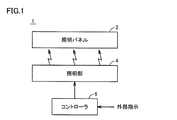
- FIG. 1 is a schematic block diagram illustrating a configuration of lighting apparatus 1 according to the present embodiment.
- lighting device 1 includes lighting panel 2, lighting unit 4 including a light emitting element, and controller 6 that controls lighting device 1 as a whole.
- the illumination panel 2 irradiates the light emitted from the light emitting element of the illumination unit 4 as uniform light. In addition, you may make it irradiate a specific spot area
- the illumination unit 4 includes a plurality of light emitting elements each having a different emission spectrum.
- a case where three types of light emitting elements are provided will be described as an example. Specifically, a light-emitting element having a light emission spectrum of red (Red), green (Green), and blue (Blue) is provided. In this example, three types of light emitting elements will be described.
- the present invention is not limited to this, and any configuration may be adopted as long as a plurality (two or more) are connected in series. Further, a structure in which a light-emitting element is provided can be employed.
- examples of light-emitting elements constituting these include organic EL (also referred to as OLED: Organic Light Emitting Diode, or Organic Electroluminescence). Alternatively, a light emitting diode (LED) may be used.
- the illumination device 1 may further include other light emitting elements in addition to these.
- the controller 6 instructs the illumination unit 4 to perform light emission control. Specifically, a control signal for adjusting the luminance of the illumination unit 4 is output to the illumination unit 4 in accordance with an instruction from the outside (instruction for luminance adjustment).
- FIG. 2 is a schematic configuration diagram of light emitting element group 15 of illumination unit 4 according to the present embodiment.
- the case where organic EL is used as a light emitting element is shown as an example.
- a red light emitting element (red light emitting layer) 10 a green light emitting element (green light emitting layer) 12, and a blue light emitting element (blue light emitting layer) 14 are laminated, and the light emitting layer of each color light emitting element is an electrode 15A, It is clamped by 15B, 15C, and 15D, respectively.
- each color light emitting layer emits light.
- the drive unit 16 drives the current supplied to the electrodes 15A, 15B, 15C, and 15D according to the control from the controller 6, thereby adjusting the luminance balance of the light emitting elements of each color and emitting light from the lighting device 1.
- the dimming and toning of light can be controlled.
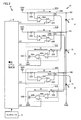
- FIG. 3 is a diagram illustrating a specific configuration of illumination unit 4 according to the present embodiment.
- the illumination unit 4 includes a light emitting element group 15 and a drive unit 16.
- the light emitting element group 15 includes a plurality of light emitting elements connected in series as described above.
- the organic ELs 10, 12, and 14 connected in series with different emission spectra will be described.
- the organic EL may be a single element or a string configuration in which a plurality of elements are connected.
- the organic EL 10 is provided between the node N0 and the node N1.
- the organic EL 12 is provided between the node N1 and the node N2.
- the organic EL 14 is provided between the node N3 and the ground voltage GND.
- a supply current adjustment circuit 20A is provided between the power supply voltage VDD and the node N0 for the organic EL 10.
- a supply current adjustment circuit 20B is provided between the power supply voltage VDD and the node N1 in parallel with the supply current adjustment circuit 20A for the organic EL 12.
- a supply current adjustment circuit 20C is provided between the power supply voltage VDD and the node N2 in parallel with the supply current adjustment circuit 20B for the organic EL 14.
- a discharge current adjusting circuit 30A is provided corresponding to the node N1 and for discharging a current flowing through the organic EL 10 between the node N1 and the ground voltage GND.
- a discharge current adjusting circuit 30B is provided corresponding to the node N2 and for discharging a current flowing through the organic EL 12 between the node N2 and the ground voltage GND.
- the voltage level setting unit 8 generates and outputs the reference voltages V1 to V3 for defining the current flowing through each of the organic ELs 10, 12, and 14 in accordance with instructions from the controller 6.
- the driving unit 16 includes a voltage level setting unit 8 and sets a reference voltage according to a control signal from the controller 6.
- the controller 6 in this example instructs the voltage level setting unit 8 to set a reference voltage associated with the luminance as a control signal for adjusting the luminance of each organic EL.
- the supply current adjustment circuit 20A is a circuit that supplies a predetermined constant current I1 corresponding to the reference voltage V1 to the node N0.
- the supply current adjustment circuit 20A includes a resistance element 22A, a transistor 24A, an amplifier 26A, and a comparator 28A.
- Resistance element 22A and transistor 24A are connected in series between power supply voltage VDD and node N0. Then, the amplifier 26A measures the voltage (potential difference) across the resistance element 22A based on the current value passing through the resistance element 22A, amplifies it, and outputs it to the comparator 28A.
- the comparator 28A compares the voltage output from the amplifier 26A with the reference voltage V1 for defining the amount of current to pass, and outputs a control voltage based on the comparison result to the gate of the transistor 24A.
- the voltage level setting unit 8 generates a reference voltage that is set according to the target current value, and outputs the reference voltage to the comparator 28A.
- the comparator 28A compares the voltage output from the amplifier 26A with the reference voltage V1, and raises the voltage level of the control voltage if the reference voltage V1 is greater than the voltage output from the amplifier 26A. As a result, the current passing through the transistor 24A increases, and the process is repeated until the output of the amplifier 26A increases and becomes the same value as the reference voltage V1.
- the reference voltage V1 is smaller than the voltage output from the amplifier 26A, the voltage level of the control voltage is lowered. As a result, the current passing through the transistor 24A decreases, and the process is repeated until the output of the amplifier 26A decreases and becomes the same value as the reference voltage V1.
- the discharge current adjusting circuit 30A is provided for the organic EL 10, and discharges (pulls out) a predetermined constant current I1 corresponding to the reference voltage V1 from a node N1 (connection node) between the organic EL 10 and the organic EL 12. ) Circuit.
- the discharge current adjustment circuit 30A includes a resistance element 32A, a transistor 34A, an amplifier 36A, and a comparator 38A.
- Resistance element 32A and transistor 34A are connected in series between node N1 and ground voltage GND.
- the amplifier 36A measures the voltage (potential difference) across the resistance element 32A based on the current value passing through the resistance element 32A, amplifies it, and outputs it to the comparator 38A.
- the comparator 38A compares the voltage output from the amplifier 36A with the reference voltage V1 for defining the amount of current to pass, and outputs a control voltage based on the comparison result to the gate of the transistor 34A.
- the voltage level setting unit 8 generates a reference voltage V1 that is set according to the target current value, and outputs the reference voltage V1 to the comparator 38A.
- the comparator 38A compares the voltage output from the amplifier 36A with the reference voltage V1, and if the reference voltage V1 is greater than the voltage output from the amplifier 36A, the comparator 38A increases the voltage level of the control voltage. As a result, the current passing through the transistor 34A increases, and the process is repeated until the output of the amplifier 36A increases and becomes the same value as the reference voltage V1.
- the reference voltage V1 is smaller than the voltage output from the amplifier 36A, the voltage level of the control voltage is lowered. As a result, the current passing through the transistor 34A decreases, the output of the amplifier 36A decreases, and this process is repeated until it reaches the same value as the reference voltage V1.
- the circuit can discharge a target current corresponding to the reference voltage V1. Since the other discharge current adjusting circuits have the same configuration, detailed description thereof will not be repeated.
- the supply current adjustment circuit 20A is provided to the organic EL 10 and the current amount I1 is supplied according to the reference voltage V1. Further, a discharge current adjustment circuit 30A is provided for the organic EL 10, and the current amount I1 is discharged according to the reference voltage V1.
- a supply current adjusting circuit 20B is provided for the organic EL 12, and the current amount I2 is supplied according to the reference voltage V2.
- a discharge current adjusting circuit 30B is provided for the organic EL 12, and the current amount I2 is discharged through the node N2 between the organic EL 12 and the organic EL 14 according to the reference voltage V2.
- a supply current adjusting circuit 20C is provided for the organic EL 14, and the current amount I3 is supplied according to the reference voltage V3.
- the supplied current amount I3 flows directly to the ground side and does not flow to other organic ELs. Therefore, it is not necessary to provide a discharge current adjusting circuit for the organic EL 14.
- upstream light emitting elements that are electrically connected directly to downstream light emitting elements such as organic ELs 12 and 14 (two light emitting elements that are directly connected in this way
- a current supplied from a supply current adjusting circuit provided for the light emitting element) is discharged by the discharge current adjusting circuit via a connection node between two adjacent light emitting elements.
- current supplied from a supply current adjusting circuit provided for a light emitting element to which no light emitting element is connected downstream flows into the ground side. Therefore, the current flowing out from the upstream light emitting element does not flow into the downstream light emitting element. Therefore, it is possible to independently control the amount of current flowing to each light emitting element.
- the voltage level setting unit 8 may set the reference voltage input to the supply current adjustment circuit 20A and the discharge current adjustment circuit 30A to the reference voltage V1 in order to set the current amount I1 for the organic EL 10. .
- the voltage level setting unit 8 may set the reference voltage input to the supply current adjustment circuit 20B and the discharge current adjustment circuit 30B to the reference voltage V2 in order to set the current amount I2 for the organic EL 12.
- the voltage level setting unit 8 may set the reference voltage input to the supply current adjusting circuit 30C to the reference voltage V3 in order to set the current amount I3 for the organic EL 14.
- each light emitting element is set by setting a reference voltage output to a supply current adjusting circuit and a discharge current adjusting circuit provided for each light emitting element.
- the current flowing through each can be adjusted independently. Specifically, out of two adjacent light emitting elements, the current supplied to the upstream light emitting element through the supply current adjusting circuit is all discharged from the connection node between the downstream light emitting elements. The current is discharged through the adjusting circuit, and a current is newly supplied to the downstream light emitting element through the supply current adjusting circuit based on the reference voltage set for the downstream light emitting element.
- the reference voltage output to the supply current adjustment circuit 20A and the discharge current adjustment circuit 30A may be adjusted to be set to different voltage values and adjusted to a desired current amount. The same applies to other reference voltages.
- the supply current adjustment circuit and the discharge current adjustment circuit have been described using the configuration of the constant current source circuit, but it is naturally possible to use the configuration of the constant voltage source circuit.
Landscapes
- Physics & Mathematics (AREA)
- Optics & Photonics (AREA)
- Circuit Arrangement For Electric Light Sources In General (AREA)
- Electroluminescent Light Sources (AREA)
Abstract
照明装置は、直列に接続された発光スペクトルが各々異なる複数の発光素子と、複数の発光素子を駆動するための駆動装置とを備える。駆動装置は、各発光素子にそれぞれ対応して設けられ、対応する発光素子に対して供給する電流量を調整するための供給電流調整回路と、複数の発光素子のうち隣接する2つの発光素子の間にある接続ノードにそれぞれ対応して設けられ、2つの発光素子のうち接続ノードと接続された上流側の発光素子から接続ノードを介して排出する電流量を調整するための排出電流調整回路とを含む。排出電流調整回路により排出する電流量は、対応する発光素子に対して設けられた供給電流調整回路から供給する電流量と同じ値に設定される。
Description
本発明は、定電流源に直列接続された複数の発光素子を備える照明装置に関する。
特表2010-524221号公報(特許文献1)は、発光ダイオードの駆動方法に関する発明を開示している。この駆動方法は、直列接続の発光ダイオードの輝度を個々に調整可能な構成が示されている。
具体的には、主電流を供給して、当該主電流に対して発光ダイオード間の中間電極から引かれる電流を制御することにより、直列接続された各発光ダイオードに流れる電流量を調整する駆動方式が開示されている。
しかしながら、当該特表2010-524221号公報(特許文献1)に開示される駆動方式では、主電流に対して中間電極から引かれる電流を常に演算して制御する必要がある。特に3つの発光ダイオードを直列接続する場合、最終段の発光ダイオードに流す電流は、前段の発光ダイオードに流れる電流に律則されるため演算調整が必要であり、回路構成が複雑になるという問題がある。
本発明は、複数の発光素子が直列に接続された構成において、簡易に各発光素子に流れる電流量を個々独立に調整することが可能な照明装置を提供することを目的とする。
本発明のある局面に従う照明装置は、直列に接続された発光スペクトルが各々異なる複数の発光素子と、複数の発光素子を駆動するための駆動装置とを備える。駆動装置は、各発光素子にそれぞれ対応して設けられ、対応する発光素子に対して供給する電流量を調整するための供給電流調整回路と、複数の発光素子のうち隣接する2つの発光素子の間にある接続ノードにそれぞれ対応して設けられ、2つの発光素子のうち接続ノードと接続された上流側の発光素子から接続ノードを介して排出する電流量を調整するための排出電流調整回路とを含む。排出電流調整回路により排出する電流量は、対応する発光素子に対して設けられた供給電流調整回路から供給する電流量と同じ値に設定される。
複数の発光素子が直列に接続された構成において、簡易に各発光素子に流れる電流量を個々独立に調整することが可能である。
本実施の形態について、以下、図面を参照しながら説明する。実施の形態の説明において、個数および量などに言及する場合、特に記載がある場合を除き、本発明の範囲は必ずしもその個数およびその量などに限定されない。実施の形態の説明において、同一の部品および相当部品に対しては、同一の参照番号を付し、重複する説明は繰り返さない場合がある。特に制限が無い限り、実施の形態に示す構成に示す構成を適宜組み合わせて用いることは、当初から予定されていることである。
(全体構成)
図1は、本実施の形態に従う照明装置1の構成を説明する概略ブロック図である。
図1は、本実施の形態に従う照明装置1の構成を説明する概略ブロック図である。
図1を参照して、照明装置1は、照明パネル2と、発光素子を含む照明部4と、照明装置1全体を制御するコントローラ6とを含む。
照明パネル2は、照明部4の発光素子から発光された光を均一にした光として照射する。なお、レンズ等を設けて指向性を持たせることにより特定のスポット領域を照射するようにしても良い。
照明部4は、発光スペクトラムが各々異なる複数の発光素子を含む。本例においては、一例として3種類の発光素子が設けられる場合について説明する。具体的には、赤(Red)、緑(Green)、青(Blue)色の発光スペクトラムを有する発光素子を有する。なお、本例においては、3種類の発光素子について説明するが、特にこれに限られず、複数(2以上)が直列に接続される構成であれば、どのような構成を採用しても良く、さらに発光素子を設ける構成とすることが可能である。
なお、これらを構成する発光素子としては、有機EL(OLED:Organic Light Emitting Diode、若しくはOrganic Electroluminescenceともいう)等が挙げられる。あるいは、発光ダイオード(LED:Light Emitting Diode)等であってもよい。照明装置1は、これらに加えて他の発光素子をさらに備えていてもよい。
コントローラ6は、照明部4に対して発光制御を指示する。具体的には、外部からの指示(輝度調整の指示)に従って照明部4の輝度を調整するための制御信号を照明部4に出力する。
図2は、本実施の形態に従う照明部4の発光素子群15の概略構成図である。
図2を参照して、本例においては、一例として発光素子として有機ELを用いた場合が示されている。具体的には、赤色発光素子(赤色発光層)10、緑色発光素子(緑色発光層)12および青色発光素子(青色発光層)14が積層されており、各色発光素子の発光層が電極15A,15B,15C,15Dでそれぞれ挟持されている。
図2を参照して、本例においては、一例として発光素子として有機ELを用いた場合が示されている。具体的には、赤色発光素子(赤色発光層)10、緑色発光素子(緑色発光層)12および青色発光素子(青色発光層)14が積層されており、各色発光素子の発光層が電極15A,15B,15C,15Dでそれぞれ挟持されている。
各電極15A,15B,15C,15Dに駆動部16を介して外部電源から給電することにより、各色発光層が発光する。このとき、各電極15A,15B,15C,15Dに供給される電流を駆動部16がコントローラ6からの制御に従って駆動することにより、各色発光素子の輝度バランスを調光し、照明装置1から発光される光の調光および調色を制御することができる。
(具体的構成)
図3は、本実施の形態に従う照明部4の具体的構成を説明する図である。
図3は、本実施の形態に従う照明部4の具体的構成を説明する図である。
図3を参照して、照明部4は、発光素子群15と駆動部16とを含む。発光素子群15は、上述したように直列に接続された複数の発光素子を含む。
本例においては、発光スペクトラムがそれぞれ異なる直列に接続された有機EL10、12、14について説明する。なお、当該有機ELは、単体の素子でもよいし、複数の素子が接続されたストリングスの構成であっても良い。
有機EL10は、ノードN0とノードN1との間に設けられる。また、有機EL12は、ノードN1とノードN2との間に設けられる。有機EL14は、ノードN3と接地電圧GNDとの間に設けられる。有機EL10に対して電源電圧VDDとノードN0との間に供給電流調整回路20Aが設けられる。
また、有機EL12に対して供給電流調整回路20Aと並列に電源電圧VDDとノードN1との間に供給電流調整回路20Bが設けられる。
また、有機EL14に対して供給電流調整回路20Bと並列に電源電圧VDDとノードN2との間に供給電流調整回路20Cが設けられる。
また、ノードN1に対応して設けられ、ノードN1と接地電圧GNDとの間に有機EL10に流れる電流を排出するための排出電流調整回路30Aが設けられる。
また、ノードN2に対応して設けられ、ノードN2と接地電圧GNDとの間に有機EL12に流れる電流を排出するための排出電流調整回路30Bが設けられる。
本例において、電圧レベル設定部8は、コントローラ6からの指示に従って各有機EL10,12,14の各々に流れる電流を規定するための基準電圧V1~V3を生成して出力する。
また、駆動部16は、電圧レベル設定部8を含み、コントローラ6からの制御信号に従って基準電圧を設定する。
本例におけるコントローラ6は、一例として各有機ELの輝度を調整するための制御信号として、輝度に対応付けられた基準電圧を設定するように電圧レベル設定部8に対して指示する。
(供給電流調整回路の構成)
供給電流調整回路の構成について説明する。
供給電流調整回路の構成について説明する。
供給電流調整回路20A~20Cの構成は全て同じ構成であるため、その1つの構成である供給電流調整回路20Aについて代表的に説明する。当該供給電流調整回路は、基準電圧V1に応じた所定の定電流I1をノードN0に供給する回路である。
供給電流調整回路20Aは、抵抗素子22Aと、トランジスタ24Aと、増幅器26Aと、比較器28Aとを含む。
抵抗素子22Aおよびトランジスタ24Aは、電源電圧VDDとノードN0との間に直列に接続される。そして、増幅器26Aは、抵抗素子22Aを通過する電流値に基づく抵抗素子22Aの両端電圧(電位差)を計測して、それを増幅して比較器28Aに出力する。
比較器28Aは、増幅器26Aから出力された電圧と、通過する電流量を規定するための基準電圧V1とを比較して比較結果に基づく制御電圧をトランジスタ24Aのゲートに出力する。
電圧レベル設定部8は、目標電流値に応じて設定される基準電圧を生成して、比較器28Aに出力する。比較器28Aは、増幅器26Aから出力された電圧と、基準電圧V1とを比較して、基準電圧V1が増幅器26Aから出力された電圧よりも大きければ、制御電圧の電圧レベルを上げる。これによりトランジスタ24Aを通過する電流は増加し、増幅器26Aの出力が大きくなり、基準電圧V1と同じ値となるまで当該処理が繰り返される。
一方、基準電圧V1が増幅器26Aから出力された電圧よりも小さければ、制御電圧の電圧レベルを下げる。これによりトランジスタ24Aを通過する電流は減少し、増幅器26Aの出力が小さくなり、基準電圧V1と同じ値となるまで当該処理が繰り返される。
当該回路により基準電圧V1に応じた目標電流を供給することが可能となる。
なお、他の供給電流調整回路についても同様の構成であるためその詳細な説明は繰り返さない。
なお、他の供給電流調整回路についても同様の構成であるためその詳細な説明は繰り返さない。
(排出電流調整回路の構成)
排出電流調整回路の構成について説明する。
排出電流調整回路の構成について説明する。
排出電流調整回路30A,30Bの構成は全て同じ構成であるため、その1つの構成である排出電流調整回路30Aについて代表的に説明する。当該排出電流調整回路30Aは、有機EL10に対して設けられ、基準電圧V1に応じた所定の定電流I1を、有機EL10と有機EL12との間にあるノードN1(接続ノード)から排出する(引き抜く)回路である。
排出電流調整回路30Aは、抵抗素子32Aと、トランジスタ34Aと、増幅器36Aと、比較器38Aとを含む。
抵抗素子32Aおよびトランジスタ34Aは、ノードN1と接地電圧GNDとの間に直列に接続される。そして、増幅器36Aは、抵抗素子32Aを通過する電流値に基づく抵抗素子32Aの両端電圧(電位差)を計測して、それを増幅して比較器38Aに出力する。
比較器38Aは、増幅器36Aから出力された電圧と、通過する電流量を規定するための基準電圧V1とを比較して比較結果に基づく制御電圧をトランジスタ34Aのゲートに出力する。
電圧レベル設定部8は、目標電流値に応じて設定される基準電圧V1を生成して、比較器38Aに出力する。比較器38Aは、増幅器36Aから出力された電圧と、基準電圧V1とを比較して、基準電圧V1が増幅器36Aから出力された電圧よりも大きければ、制御電圧の電圧レベルを上げる。これによりトランジスタ34Aを通過する電流は増加し、増幅器36Aの出力が大きくなり、基準電圧V1と同じ値となるまで当該処理が繰り返される。
一方、基準電圧V1が増幅器36Aから出力された電圧よりも小さければ、制御電圧の電圧レベルを下げる。これによりトランジスタ34Aを通過する電流は減少し、増幅器36Aの出力が小さくなり、基準電圧V1と同じ値となるまで当該処理が繰り返される。
当該回路により基準電圧V1に応じた目標電流を排出することが可能となる。
なお、他の排出電流調整回路についても同様の構成であるためその詳細な説明は繰り返さない。
なお、他の排出電流調整回路についても同様の構成であるためその詳細な説明は繰り返さない。
(駆動方式の説明)
本実施の形態においては、上記で説明したように有機EL10に対して、供給電流調整回路20Aが設けられて基準電圧V1に従って電流量I1が供給される。また、有機EL10に対して、排出電流調整回路30Aが設けられて基準電圧V1に従って電流量I1が排出される。
本実施の形態においては、上記で説明したように有機EL10に対して、供給電流調整回路20Aが設けられて基準電圧V1に従って電流量I1が供給される。また、有機EL10に対して、排出電流調整回路30Aが設けられて基準電圧V1に従って電流量I1が排出される。
したがって、供給電流調整回路20Aから供給された電流は、ノードN1を経て全て排出電流調整回路30Aを介して排出されることになる。
また、有機EL12に対して供給電流調整回路20Bが設けられて、基準電圧V2に従って電流量I2が供給される。また、有機EL12に対して排出電流調整回路30Bが設けられて、基準電圧V2に従って、有機EL12と有機EL14との間にあるノードN2を経て電流量I2が排出される。
したがって、供給電流調整回路20Bから供給された電流は、全て排出電流調整回路30Bを介して排出されることになる。
また、有機EL14に対して供給電流調整回路20Cが設けられて基準電圧V3に従って電流量I3が供給される。供給された電流量I3はそのまま接地側へ流れ込み、他の有機ELに流れることはない。したがって、有機EL14に対しては排出電流調整回路を設けなくてもよい。
以上のとおり、有機EL12,14のように下流側の発光素子と電気的に直接接続されている上流側の発光素子(このように直接接続される2つの発光素子を、便宜上、隣接する2つの発光素子ともいう)に対して設けられた供給電流調整回路から供給される電流は、隣接する2つの発光素子の間にある接続ノードを介して排出電流調整回路により排出される。また、有機EL16のように、下流側に発光素子が接続されていない発光素子に対して設けられた供給電流調整回路から供給される電流は、接地側に流れ込む。したがって、上流側の発光素子から流れ出る電流が下流側の発光素子に流れ込むことはない。それゆえ、それぞれの発光素子に対して流れる電流量を独立制御することが可能である。
具体的には、電圧レベル設定部8は、有機EL10に対して電流量I1を設定するために供給電流調整回路20Aおよび排出電流調整回路30Aに入力する基準電圧を基準電圧V1に設定すれば良い。
また、電圧レベル設定部8は、有機EL12に対して電流量I2を設定するために供給電流調整回路20Bおよび排出電流調整回路30Bに入力する基準電圧を基準電圧V2に設定すれば良い。
また、電圧レベル設定部8は、有機EL14に対して電流量I3を設定するために供給電流調整回路30Cに入力する基準電圧を基準電圧V3に設定すれば良い。
以上のように、複数の発光素子が直列に接続された構成において、各発光素子に対して設けられた供給電流調整回路および排出電流調整回路に出力する基準電圧を設定することにより、各発光素子に流れる電流を個々独立に調整することができる。具体的には、隣接する2つの発光素子のうち、上流側の発光素子に対して供給電流調整回路を通じて供給された電流量を全て、下流側の発光素子との間にある接続ノードから排出電流調整回路を通じて排出し、下流側の発光素子に対しては、下流側の発光素子に対して設定された基準電圧に基づき新たに供給電流調整回路を通じて電流を供給する。そのため、従来構成の如く、発光素子間の中間電極から引かれる電流を演算して個々の発光素子に流れる電流を制御する必要はなく、簡易な構成で、各発光素子に供給される電流量を個別独立して制御することが可能である。
なお、本例においては、電圧レベル設定部8から供給電流調整回路20Aと、排出電流調整回路30Aとに出力する基準電圧V1について同じ基準電圧の電圧値を設定する場合について説明したが、製造時の素子のばらつき等により基準電圧に応じた電流量にばらつきが生じる場合も考えられる。当該場合には、供給電流調整回路20Aと、排出電流調整回路30Aとに出力する基準電圧をそれぞれ調整して異なる電圧値に設定するようにして所望の電流量に調整するようにしても良い。他の基準電圧についても同様である。
なお、本例においては、供給電流調整回路および排出電流調整回路について定電流源回路の構成を用いて説明したが定電圧源回路の構成を用いるようにすることも当然に可能である。
以上、本発明に基づいた実施の形態について説明したが、今回開示された実施の形態はすべての点で例示であって制限的なものではない。本発明の技術的範囲は請求の範囲によって示され、請求の範囲と均等の意味および範囲内でのすべての変更が含まれることが意図される。
1 照明装置、2 照明パネル、4 照明部、6 コントローラ、8 電圧レベル設定部、10,12,14 発光素子、15 発光素子群、15A~15D 電極、16 駆動部、20A~20C 供給電流調整回路、30A,30B 排出電流調整回路。
Claims (5)
- 直列に接続された発光スペクトルが各々異なる複数の発光素子と、
前記複数の発光素子を駆動するための駆動装置とを備え、
前記駆動装置は、
各前記発光素子にそれぞれ対応して設けられ、対応する発光素子に対して供給する電流量を調整するための供給電流調整回路と、
前記複数の発光素子のうち隣接する2つの発光素子の間にある接続ノードにそれぞれ対応して設けられ、前記2つの発光素子のうち前記接続ノードと接続された上流側の発光素子から前記接続ノードを介して排出する電流量を調整するための排出電流調整回路とを含み、
前記排出電流調整回路により排出する電流量は、対応する発光素子に対して設けられた前記供給電流調整回路から供給する電流量と同じ値に設定される、照明装置。 - 前記複数の発光素子は、赤色、緑色、青色発光素子である、請求項1記載の照明装置。
- 前記供給電流調整回路および前記排出電流調整回路は、入力電圧に応じて電流量を調整し、
前記駆動装置は、前記入力電圧の電圧レベルを設定する電圧レベル設定部をさらに含む、請求項1または2記載の照明装置。 - 前記供給電流調整回路および前記排出電流調整回路のそれぞれに入力する前記入力電圧の値は同じである、請求項3に記載の照明装置。
- 前記複数の発光素子の各々は、有機ELであり、前記複数の発光素子が積層されており、前記発光素子の各々が電極で挟持されている、請求項1~4のいずれか一項に記載の照明装置。
Priority Applications (1)
| Application Number | Priority Date | Filing Date | Title |
|---|---|---|---|
| JP2014553076A JPWO2014097904A1 (ja) | 2012-12-18 | 2013-12-06 | 照明装置 |
Applications Claiming Priority (2)
| Application Number | Priority Date | Filing Date | Title |
|---|---|---|---|
| JP2012-275843 | 2012-12-18 | ||
| JP2012275843 | 2012-12-18 |
Publications (1)
| Publication Number | Publication Date |
|---|---|
| WO2014097904A1 true WO2014097904A1 (ja) | 2014-06-26 |
Family
ID=50978239
Family Applications (1)
| Application Number | Title | Priority Date | Filing Date |
|---|---|---|---|
| PCT/JP2013/082839 Ceased WO2014097904A1 (ja) | 2012-12-18 | 2013-12-06 | 照明装置 |
Country Status (2)
| Country | Link |
|---|---|
| JP (1) | JPWO2014097904A1 (ja) |
| WO (1) | WO2014097904A1 (ja) |
Cited By (2)
| Publication number | Priority date | Publication date | Assignee | Title |
|---|---|---|---|---|
| JP2019117806A (ja) * | 2019-04-24 | 2019-07-18 | パイオニア株式会社 | 発光装置 |
| WO2025156248A1 (zh) * | 2024-01-26 | 2025-07-31 | 京东方科技集团股份有限公司 | 发光器件、显示面板及显示装置 |
Citations (4)
| Publication number | Priority date | Publication date | Assignee | Title |
|---|---|---|---|---|
| JP2007165001A (ja) * | 2005-12-09 | 2007-06-28 | Nec Lighting Ltd | Led点灯装置 |
| JP2008130989A (ja) * | 2006-11-24 | 2008-06-05 | Matsushita Electric Works Ltd | Led点灯回路およびそれを用いる照明器具 |
| JP2009289940A (ja) * | 2008-05-29 | 2009-12-10 | Mitsubishi Electric Corp | 発光装置及び照明装置 |
| JP2011222123A (ja) * | 2010-04-02 | 2011-11-04 | Sharp Corp | 照明装置 |
Family Cites Families (2)
| Publication number | Priority date | Publication date | Assignee | Title |
|---|---|---|---|---|
| JP2010021063A (ja) * | 2008-07-11 | 2010-01-28 | Canon Inc | 有機el表示装置 |
| KR100995793B1 (ko) * | 2010-08-20 | 2010-11-22 | 김남규 | 발광 다이오드 어레이 구동회로 |
-
2013
- 2013-12-06 JP JP2014553076A patent/JPWO2014097904A1/ja active Pending
- 2013-12-06 WO PCT/JP2013/082839 patent/WO2014097904A1/ja not_active Ceased
Patent Citations (4)
| Publication number | Priority date | Publication date | Assignee | Title |
|---|---|---|---|---|
| JP2007165001A (ja) * | 2005-12-09 | 2007-06-28 | Nec Lighting Ltd | Led点灯装置 |
| JP2008130989A (ja) * | 2006-11-24 | 2008-06-05 | Matsushita Electric Works Ltd | Led点灯回路およびそれを用いる照明器具 |
| JP2009289940A (ja) * | 2008-05-29 | 2009-12-10 | Mitsubishi Electric Corp | 発光装置及び照明装置 |
| JP2011222123A (ja) * | 2010-04-02 | 2011-11-04 | Sharp Corp | 照明装置 |
Cited By (2)
| Publication number | Priority date | Publication date | Assignee | Title |
|---|---|---|---|---|
| JP2019117806A (ja) * | 2019-04-24 | 2019-07-18 | パイオニア株式会社 | 発光装置 |
| WO2025156248A1 (zh) * | 2024-01-26 | 2025-07-31 | 京东方科技集团股份有限公司 | 发光器件、显示面板及显示装置 |
Also Published As
| Publication number | Publication date |
|---|---|
| JPWO2014097904A1 (ja) | 2017-01-12 |
Similar Documents
| Publication | Publication Date | Title |
|---|---|---|
| US7482760B2 (en) | Method and apparatus for scaling the average current supply to light-emitting elements | |
| KR101428430B1 (ko) | 조명 장치용 집적 회로 및 조명 장치 | |
| US7847783B2 (en) | Controller circuitry for light emitting diodes | |
| JP4971949B2 (ja) | 駆動電流安定化制御装置を備える発光ダイオードのドライバーとその発光ダイオードのドライバーを用いたバックライトシステム | |
| CN104303595A (zh) | 用于基于发光二极管的照明系统的电流平衡电路 | |
| US20120319602A1 (en) | Light emitting device and illumination apparatus having same | |
| US20120153845A1 (en) | Solid state lighting control methods and apparatuses for series combinations of light emitting diodes | |
| CN104081530A (zh) | 包括对led节点敏感的电流分流的发光设备和相关方法 | |
| US20050273237A1 (en) | Control method and control structure for lighting system | |
| WO2014097904A1 (ja) | 照明装置 | |
| US20130278156A1 (en) | Light-emitting diode lighting apparatus, illuminating apparatus and illuminating method | |
| JP6152290B2 (ja) | バックライト装置ならびにそれを用いたディスプレイ装置および電子機器 | |
| US9078302B2 (en) | Apparatus for controlling an illumination device and method for controlling an illumination device | |
| WO2014087874A1 (ja) | 照明装置 | |
| JP5637341B1 (ja) | 照明装置 | |
| JP2008171983A (ja) | 光源装置、画像表示装置、プロジェクタおよび光源制御方法 | |
| EP3331327B1 (en) | Led illumination system, led illumination device, and brightness adjustment method for led illumination device | |
| JP6296051B2 (ja) | 照明装置 | |
| CN101950535A (zh) | 发光装置与相关驱动方法 | |
| WO2012153594A1 (ja) | 照明装置 | |
| US9615421B1 (en) | LED control circuit | |
| KR101988660B1 (ko) | Led 모듈 구동 회로 | |
| KR101548181B1 (ko) | 광 편차의 조정 기능을 갖는 교류 led 구동회로 | |
| JP2013016693A (ja) | Led選択方法、及びled光源ユニットの製造方法 |
Legal Events
| Date | Code | Title | Description |
|---|---|---|---|
| 121 | Ep: the epo has been informed by wipo that ep was designated in this application |
Ref document number: 13866181 Country of ref document: EP Kind code of ref document: A1 |
|
| ENP | Entry into the national phase |
Ref document number: 2014553076 Country of ref document: JP Kind code of ref document: A |
|
| NENP | Non-entry into the national phase |
Ref country code: DE |
|
| 122 | Ep: pct application non-entry in european phase |
Ref document number: 13866181 Country of ref document: EP Kind code of ref document: A1 |