WO2014092192A1 - 酸化物半導体素子、酸化物半導体素子の製造方法、表示装置、イメージセンサ及びx線センサ - Google Patents
酸化物半導体素子、酸化物半導体素子の製造方法、表示装置、イメージセンサ及びx線センサ Download PDFInfo
- Publication number
- WO2014092192A1 WO2014092192A1 PCT/JP2013/083529 JP2013083529W WO2014092192A1 WO 2014092192 A1 WO2014092192 A1 WO 2014092192A1 JP 2013083529 W JP2013083529 W JP 2013083529W WO 2014092192 A1 WO2014092192 A1 WO 2014092192A1
- Authority
- WO
- WIPO (PCT)
- Prior art keywords
- layer
- oxide semiconductor
- insulating protective
- tft
- layers
- Prior art date
- Legal status (The legal status is an assumption and is not a legal conclusion. Google has not performed a legal analysis and makes no representation as to the accuracy of the status listed.)
- Ceased
Links
Images






Classifications
-
- H—ELECTRICITY
- H10—SEMICONDUCTOR DEVICES; ELECTRIC SOLID-STATE DEVICES NOT OTHERWISE PROVIDED FOR
- H10D—INORGANIC ELECTRIC SEMICONDUCTOR DEVICES
- H10D30/00—Field-effect transistors [FET]
- H10D30/60—Insulated-gate field-effect transistors [IGFET]
- H10D30/67—Thin-film transistors [TFT]
- H10D30/674—Thin-film transistors [TFT] characterised by the active materials
- H10D30/6755—Oxide semiconductors, e.g. zinc oxide, copper aluminium oxide or cadmium stannate
-
- H—ELECTRICITY
- H10—SEMICONDUCTOR DEVICES; ELECTRIC SOLID-STATE DEVICES NOT OTHERWISE PROVIDED FOR
- H10F—INORGANIC SEMICONDUCTOR DEVICES SENSITIVE TO INFRARED RADIATION, LIGHT, ELECTROMAGNETIC RADIATION OF SHORTER WAVELENGTH OR CORPUSCULAR RADIATION
- H10F39/00—Integrated devices, or assemblies of multiple devices, comprising at least one element covered by group H10F30/00, e.g. radiation detectors comprising photodiode arrays
- H10F39/011—Manufacture or treatment of image sensors covered by group H10F39/12
- H10F39/026—Wafer-level processing
-
- H—ELECTRICITY
- H10—SEMICONDUCTOR DEVICES; ELECTRIC SOLID-STATE DEVICES NOT OTHERWISE PROVIDED FOR
- H10F—INORGANIC SEMICONDUCTOR DEVICES SENSITIVE TO INFRARED RADIATION, LIGHT, ELECTROMAGNETIC RADIATION OF SHORTER WAVELENGTH OR CORPUSCULAR RADIATION
- H10F39/00—Integrated devices, or assemblies of multiple devices, comprising at least one element covered by group H10F30/00, e.g. radiation detectors comprising photodiode arrays
- H10F39/10—Integrated devices
- H10F39/12—Image sensors
- H10F39/18—Complementary metal-oxide-semiconductor [CMOS] image sensors; Photodiode array image sensors
- H10F39/189—X-ray, gamma-ray or corpuscular radiation imagers
- H10F39/1898—Indirect radiation image sensors, e.g. using luminescent members
-
- G—PHYSICS
- G02—OPTICS
- G02F—OPTICAL DEVICES OR ARRANGEMENTS FOR THE CONTROL OF LIGHT BY MODIFICATION OF THE OPTICAL PROPERTIES OF THE MEDIA OF THE ELEMENTS INVOLVED THEREIN; NON-LINEAR OPTICS; FREQUENCY-CHANGING OF LIGHT; OPTICAL LOGIC ELEMENTS; OPTICAL ANALOGUE/DIGITAL CONVERTERS
- G02F1/00—Devices or arrangements for the control of the intensity, colour, phase, polarisation or direction of light arriving from an independent light source, e.g. switching, gating or modulating; Non-linear optics
- G02F1/01—Devices or arrangements for the control of the intensity, colour, phase, polarisation or direction of light arriving from an independent light source, e.g. switching, gating or modulating; Non-linear optics for the control of the intensity, phase, polarisation or colour
- G02F1/13—Devices or arrangements for the control of the intensity, colour, phase, polarisation or direction of light arriving from an independent light source, e.g. switching, gating or modulating; Non-linear optics for the control of the intensity, phase, polarisation or colour based on liquid crystals, e.g. single liquid crystal display cells
- G02F1/133—Constructional arrangements; Operation of liquid crystal cells; Circuit arrangements
- G02F1/136—Liquid crystal cells structurally associated with a semi-conducting layer or substrate, e.g. cells forming part of an integrated circuit
- G02F1/1362—Active matrix addressed cells
- G02F1/136209—Light shielding layers, e.g. black matrix, incorporated in the active matrix substrate, e.g. structurally associated with the switching element
-
- H—ELECTRICITY
- H10—SEMICONDUCTOR DEVICES; ELECTRIC SOLID-STATE DEVICES NOT OTHERWISE PROVIDED FOR
- H10K—ORGANIC ELECTRIC SOLID-STATE DEVICES
- H10K59/00—Integrated devices, or assemblies of multiple devices, comprising at least one organic light-emitting element covered by group H10K50/00
- H10K59/10—OLED displays
- H10K59/12—Active-matrix OLED [AMOLED] displays
Definitions
- the present invention relates to an oxide semiconductor element, a method for manufacturing an oxide semiconductor element, a display device, an image sensor, and an X-ray sensor.
- An oxide semiconductor thin film can be formed at a low temperature, exhibits higher mobility than amorphous silicon, and is transparent to visible light. Therefore, a flexible TFT should be formed on a substrate such as a plastic plate or film. Is possible.
- the In—Ga—Zn—O-based oxide since the In—Ga—Zn—O-based oxide has low resistance to moisture, oxygen, contamination, etc., the In-Ga—Zn—O-based oxide is mainly used. If the oxide semiconductor layer is exposed to the atmosphere, the oxide is deteriorated over time.
- Japanese Unexamined Patent Application Publication No. 2009-14102 discloses a SiO x layer, a SiN p layer, a SiO m N n layer on the exposed surface of an oxide semiconductor layer mainly composed of an In—Ga—Zn—O-based oxide. It is disclosed that a protective layer having a three-layer structure is formed to protect the oxide semiconductor layer from moisture and the like.
- the above x, m, and n are oxygen nonstoichiometric amounts, and P is a nitrogen nonstoichiometric amount.
- International Publication No. 2009/075281 discloses a large absorption or reflection in a wavelength region of 500 nm or less on a protective layer that protects an oxide semiconductor layer mainly composed of an In—Ga—Zn—O-based oxide.
- a TFT provided with a light-shielding film made of a resin material or a metal material is disclosed.
- the protective layer has a simple three-layer structure, and the operational instability during light irradiation is not improved.
- the present invention has been made in view of the above circumstances, and an oxide semiconductor element and an oxide semiconductor element having an insulating protective layer that secures operation stability during light irradiation and suppresses generation of heat due to light irradiation. It aims at providing the manufacturing method of.
- An oxide semiconductor layer including at least one selected from the group consisting of In, Zn, Ga, and Sn, a pair of electrodes that can conduct through the oxide semiconductor layer, and the oxide semiconductor layer
- the first layer adjacent to the oxide semiconductor layer has a lower refractive index than the oxide semiconductor layer, and the second layer is the first layer in the stacking order from the oxide semiconductor layer side.
- the absolute refractive index of the second and subsequent layers is alternately different from each other in the absolute refractive index, and the thicknesses of the first and subsequent layers are defined as d (k) ( nm (k: order of stacking from the oxide semiconductor layer side), and the absolute refractive index of each layer is n (k) , 400 (nm) / 4n (k) ⁇ d (k) (nm) ⁇ And an insulating protective layer satisfying 450 (nm) / 4n (k) .
- ⁇ 2> The oxide semiconductor device according to ⁇ 1>, wherein the number of layers in the stacked structure of the insulating protective layer is an even number of 4 or more.
- ⁇ 3> The oxide semiconductor element according to ⁇ 1> or ⁇ 2>, wherein the number of layers in the stacked structure of the insulating protective layer is 8 or less.
- ⁇ 4> The odd-numbered layers in the laminated structure of the insulating protective layer are made of the same material, and the even-numbered layers of the laminated structure of the insulating protective layer are also made of the same material, ⁇ 1> to ⁇ 3> The oxide semiconductor device according to any one of 3>.
- the insulating protective layer includes any one oxide layer selected from the group consisting of Hf, Ti, Nb, Zr, and Y, and a SiO x layer (x is an oxygen non-stoichiometric amount). 1> to ⁇ 5> The oxide semiconductor device according to any one of ⁇ 5>.
- the insulating protective layer is a stack in which SiO x layers (x is an oxygen non-stoichiometric amount) and Nb 2 O y layers (y is an oxygen non-stoichiometric amount) are alternately stacked in order from the oxide semiconductor layer side.
- ⁇ 8> A method for manufacturing an oxide semiconductor device according to any one of ⁇ 1> to ⁇ 7>, comprising a step of performing a heat treatment at 300 ° C. or lower during or after the formation of the insulating protective layer. Method for manufacturing a semiconductor device.
- ⁇ 10> Any one of ⁇ 1> to ⁇ 7>, which is a thin film transistor having a gate electrode disposed through a gate insulating layer on the side opposite to the side on which the insulating protective layer is disposed.
- An X-ray sensor comprising the oxide semiconductor element according to ⁇ 10>.
- the insulating protective layer ensures operational stability during light irradiation and suppresses generation of heat due to light irradiation.
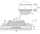
- FIG. 4 is a schematic diagram showing an example of a top contact type TFT with a bottom gate structure, which is a TFT according to an embodiment of the present invention.
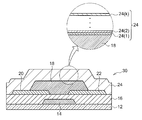
- FIG. 2 is a schematic diagram showing an example of a bottom contact type TFT with a bottom gate structure according to an embodiment of the present invention.
- 1 is a schematic cross-sectional view of a part of a liquid crystal display device according to an embodiment of an electro-optical device of the invention.
- the schematic block diagram of the electrical wiring of the liquid crystal display device shown in FIG. 3 is shown.
- 1 is a schematic cross-sectional view of a part of an active matrix organic EL display device according to an embodiment of an electro-optical device of the invention.
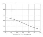
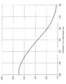
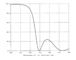
- FIG. 5 It is a simulation result of the light reflectivity of an insulation protective layer (three layer structure) about TFT of Example 1.
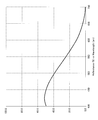
- FIG. It is a simulation result of the light reflectivity of an insulation protective layer (4 layer structure) about TFT of Example 2.
- FIG. It is a simulation result of the light reflectivity of an insulation protective layer (6 layer structure) about TFT of Example 3.
- FIG. It is a simulation result of the light reflectivity of an insulation protective layer (8 layer structure) about TFT of Example 4.
- FIG. It is a simulation result of the light reflectivity of an insulation protective layer (4 layer structure: wavelength 400nm and thickness design) about TFT of Example 5.
- FIG. It is a simulation result of the light reflectivity of an insulation protective layer (4 layer structure: wavelength 450nm thickness design) about TFT of Example 6.
- FIG. It is a simulation result of the light reflectivity of an insulation protective layer (4 layer structure: wavelength 450nm thickness design
- FIG. 7 It is a simulation result of the light reflectivity of an insulation protective layer (4 layer structure: thickness design by the combination of wavelength 450nm and wavelength 400nm) about TFT of Example 7.
- an insulating protective layer a simulation result of reflectance of light (4-layer Nb 2 O y layer changes to SiN p layer).
- FIG. It is a simulation result of the light reflectivity of an insulation protective layer (2 layer structure: thickness setting existence) about TFT of the comparative example 2.
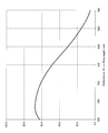
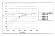
- FIG. 5 is a graph plotting the calculation results of ⁇ Vth for each wavelength in Examples 1 to 3 and Comparative Examples 1 and 2, with the wavelength as the horizontal axis and ⁇ Vth as the vertical axis. It is a simulation result of the light reflectivity of an insulation protective layer (10 layer structure) about TFT of Example 9. FIG. It is a simulation result of the light reflectivity of an insulating protective layer (11 layer structure) about TFT of Example 10. FIG.
- Oxide Semiconductor Element Schematic Configuration of Thin Film Transistor
- An oxide semiconductor element according to an embodiment of the present invention is a thin film transistor: TFT, photodiode, or the like.
- TFT thin film transistor
- photodiode photodiode
- a TFT will be described as an example of the oxide semiconductor element.
- the TFT includes at least a gate electrode, a gate insulating layer, an oxide semiconductor layer, a source electrode, and a drain electrode, and controls a current flowing through the oxide semiconductor layer by applying a voltage to the gate electrode, and the source electrode and the drain. It is an active element having a function of switching a current between electrodes.
- the TFT element structure includes a so-called reverse stagger structure (also referred to as a bottom gate type) and a stagger structure (also referred to as a top gate type) based on the position of the gate electrode.
- the reverse stagger structure is used. It is done.
- either a so-called top contact type or bottom contact type may be employed. Note that in the top gate type, when the substrate on which the TFT is formed is the lowermost layer, the gate electrode is disposed above the gate insulating layer, and the oxide semiconductor layer is formed below the gate insulating layer.
- the bottom gate type is a mode in which a gate electrode is disposed below a gate insulating layer and an oxide semiconductor layer is formed above the gate insulating layer.
- the source / drain electrodes are formed before the oxide semiconductor layer, and the lower surface of the oxide semiconductor layer is the source / drain electrode.
- the top contact type is a form in which the oxide semiconductor layer is formed before the source / drain electrodes and the upper surface of the oxide semiconductor layer is in contact with the source / drain electrodes.
- FIG. 1 is a schematic diagram showing an example of a top contact type TFT having a bottom gate structure, which is a TFT according to an embodiment of the present invention.
- a gate electrode 14 formed on one main surface of a substrate 12, a gate insulating layer 16 covering the gate electrode 14, and a gate electrode 14 of the gate insulating layer 16 are disposed. And an oxide semiconductor layer 18 disposed on a side opposite to the side. Further, the TFT 10 includes a source electrode 20 and a drain electrode 22 that are spaced apart from each other on the side opposite to the side where the gate insulating layer 16 of the oxide semiconductor layer 18 is disposed, and the source / drain electrodes 20 and 22. And an insulating protective layer 24 stacked on the surface of the oxide semiconductor layer 18 exposed from between. And in this example, the insulating protective layer 24 is the 1st layer 24 (1) , 2nd layer 24 (2) , ... k layer 24 (k) (k: 3 or more ) from the oxide semiconductor layer 18 side. That is, a laminated structure of three or more layers.
- FIG. 2 is a schematic diagram showing an example of a bottom contact type TFT with a bottom gate structure, which is a TFT according to an embodiment of the present invention.
- the gate electrode 14 and the gate insulating layer 16 are sequentially stacked on one main surface of the substrate 12.
- a source electrode 20 and a drain electrode 22 are provided so as to be separated from each other, and an oxide semiconductor layer 18 is stacked thereon.
- the TFT 30 includes an insulating protective layer 24 that is stacked on the exposed surface of the oxide semiconductor layer 18 and has a stacked structure of three or more layers.
- the TFT according to this embodiment can have various configurations.
- an insulating layer is provided on the substrate 12, the oxide semiconductor layer 18 is formed in a plurality of layers, an oxide A configuration in which a contact layer is provided between the semiconductor layer 18 and the source / drain electrodes 20 and 22 may be employed.
- the shape, structure, size, and the like of the substrate 12 are not particularly limited on the assumption that there is a main surface on which a film can be formed, and can be appropriately selected according to the purpose.
- the structure of the substrate 12 may be a single layer structure or a laminated structure.
- the material of the substrate 12 is not particularly limited, and for example, an inorganic substrate such as glass or YSZ (yttrium stabilized zirconium), a resin substrate, a composite material thereof, or the like can be used. Among these, a resin substrate and a composite material thereof are preferable in terms of light weight and flexibility.
- the resin substrate is preferably excellent in heat resistance, dimensional stability, solvent resistance, electrical insulation, workability, low air permeability, low moisture absorption, and the like.
- the resin substrate preferably includes a gas barrier layer for preventing permeation of moisture and oxygen, an undercoat layer for improving the flatness of the resin substrate and adhesion to the lower electrode, and the like.
- the undercoat layer is formed on one side of the resin substrate, the resin substrate warps due to internal residual stress. Therefore, either coat on both sides or compress with a film quality controlled to low stress or lamination. / It is preferable to control by tensile stress.
- the undercoat layer is preferably made of a material used for the gate insulating layer 16 described later in order to improve the barrier property.
- the gate electrode 14 is formed on one main surface of the substrate 12.
- the conductive film constituting the gate electrode 14 is preferably one having high conductivity, such as a metal film such as Al, Mo, Cr, Ta, Ti, Au, Au, Al—Nd, Ag alloy, oxidation, etc.
- Metal oxide conductive films such as tin, zinc oxide, indium oxide, indium tin oxide (ITO), and zinc indium oxide (IZO) can be used.
- the gate insulating layer 16 is laminated on the surface of the gate electrode 14 opposite to the substrate 12 and on the exposed surface of the substrate 12 so as to cover the gate electrode 14.
- the insulating film constituting the gate insulating layer 16 is preferably a highly insulating film such as SiO x , SiN p , SiON, Al 2 O 3 , Y 2 O 3 , Ta 2 O 5 , HfO 2 or the like. Alternatively, an insulating film containing at least two of these compounds may be used.
- the oxide semiconductor layer 18 is stacked on the surface of the gate insulating layer 16 on the side opposite to the gate electrode 14.
- the oxide semiconductor layer 18 only needs to be mainly composed of an oxide semiconductor containing at least one selected from In, Zn, Ga, and Sn, and may further contain impurities or the like.
- the “main body” represents a component that is contained in the largest amount among the components constituting the oxide semiconductor layer 18.
- the oxide semiconductor may be either amorphous or crystalline, but an amorphous oxide semiconductor is preferably used.
- the semiconductor film is formed using an oxide semiconductor, the charge mobility is much higher than that of an amorphous silicon semiconductor film, and the semiconductor film can be driven at a low voltage.
- an oxide semiconductor is used, a semiconductor film with higher light transmittance than silicon can be formed.
- An oxide semiconductor, particularly an amorphous oxide semiconductor can be uniformly formed at a low temperature (for example, room temperature), and thus is particularly advantageous when a flexible resin substrate such as a plastic is used. .
- the constituent material of the oxide semiconductor is not particularly limited as long as it includes at least one selected from In, Zn, Ga, and Sn, but includes at least one of In, Ga, and Zn.
- An oxide for example, In—O system
- an oxide containing at least two of In, Ga, and Zn eg, In—Zn—O, In—Ga—O, and Ga—Zn—O
- the oxide containing is more preferable.
- In—Ga—Zn—O-based oxide semiconductor an oxide semiconductor whose composition in a crystalline state is represented by InGaO 3 (ZnO) m (m is a natural number less than 6) is preferable, and InGaZnO 4 is particularly preferable.
- the electron mobility tends to increase as the electrical conductivity increases.
- the layer structure of the oxide semiconductor layer 18 may be composed of two or more layers.
- the oxide semiconductor layer 18 is formed of a low resistance layer and a high resistance layer, and the low resistance layer is in contact with the gate insulating layer 16 and has a high structure. It is preferable that the resistance layer is in electrical contact with at least one of the source electrode 20 and the drain electrode 22.
- the thickness of the oxide semiconductor layer 18 is not particularly limited, but is more preferably 30 nm or more and 60 nm or less from the viewpoints of ensuring carrier movement and cost reduction.
- the source / drain electrodes 20 and 22 are formed on the surface of the oxide semiconductor layer 18 on the opposite side of the gate insulating layer 16 and spaced from each other.
- the source / drain electrodes 20 and 22 are separated from the oxide semiconductor layer 18 by the voltage applied to the gate electrode 14. Conduction is possible.
- the conductive film constituting the source / drain electrodes 20 and 22 is made of a material having high conductivity, such as a metal film such as Al, Mo, Cr, Ta, Ti, Au, Au, Al—Nd, Ag alloy, oxidation, etc.
- a metal oxide conductive film such as tin, zinc oxide, indium oxide, indium tin oxide (ITO), or indium zinc oxide (IZO) can be used.
- these conductive films can be used as a single layer structure or a laminated structure of two or more layers.
- the insulating protective layer 24 of the TFT 10 and the TFT 30 is laminated on the oxide semiconductor layer 18 exposed from between the source / drain electrodes 20 and 22 to insulate and protect the oxide semiconductor layer 18 from water, oxygen, and the like.
- the first layer 24 (1) adjacent to the oxide semiconductor layer 18 has an absolute refractive index lower than that of the oxide semiconductor layer 18.
- each of the layers 24 (2) ,..., 24 (k) after the second layer 24 (2) has an absolute refractive index relationship with the previous layer. Alternately different. Specifically, when the absolute refractive index of the oxide semiconductor layer 18 (in the case of InGaZnO 4 , the absolute refractive index of about 2.11 to 2.10 in the wavelength range of 400 nm to 450) is set to “high”, the first layer 24 ( In order from 1) , “low”, “high”, “low”, “high”,...
- the absolute refractive index in each of the first layer 24 (1) to the k-th layer 24 (k) of the insulating protective layer is the 2Sth (S is a natural number) layer in the stacking order from the oxide semiconductor layer 18 side.
- n (2S) is the absolute refractive index of the adjacent layer
- n (2S-1) and n (2S + 1) are the absolute refractive indexes of the adjacent layers.
- each layer 24 (1) , 24 (2) ,... 24 (k) is d (k) (k: stack from the oxide semiconductor layer 18 side ).
- ⁇ is an arbitrary wavelength between 400 nm and 450 nm
- n (k) is an absolute refractive index of each layer
- the thickness d (k) of each layer is a thickness represented by 430 (nm) / 4n (k).
- d (k) 430 (nm) / 4n (k)
- d (k) ⁇ / 4n (k) (400 nm ⁇ ⁇ ⁇ 450 nm)
- 400 (nm ) / 4n (k) ⁇ d (k) (nm) ⁇ 450 (nm) / 4n (k) may be satisfied.
- TFT10,30 which concerns on this embodiment, even if the light of wavelength 400nm or more and 450nm or less injects toward the oxide semiconductor layer 18 side from the outer side (opposite side of the board
- the operational stability of the TFTs 10 and 30 during light irradiation can be ensured.
- the insulating protective layer 24 reflects light, generation of heat due to light irradiation can be suppressed as compared with the case of absorbing light.
- the thickness d (k) of 24 (1) , 24 (2) ,... 24 (k) of each of the above layers may be set based on the same wavelength among wavelengths of 400 nm or more and 450 nm or less. Is preferably set based on different wavelengths. This is because light having a plurality of wavelengths is reflected, and the amount of light hitting the oxide semiconductor layer 18 is further suppressed.
- the thickness d (k) is represented using different wavelengths from each other, each layer 24 (1), 24 (2), the thickness of the at least two layers of ⁇ ⁇ ⁇ 24 (k) d (k) is The wavelength may be expressed using different wavelengths among wavelengths of 400 nm to 450 nm. For example, the thickness of each odd-numbered layer may be represented by a wavelength of 400 nm, and the thickness of each even-numbered layer may be represented by a wavelength of 450 nm.
- the number of layers in the laminated structure is preferably an even number of 4 or more.
- the TFTs 10 and 30 are used in a liquid crystal display device or the like described later, a material used for an interlayer insulating layer laminated on the insulating protective layer 24 (SiO x is often used)
- the insulating protective layer 24 (k) of the insulating protective layer 24 is 1 or more (in the combination of materials, for example, SiO x And N 2 O y ), and the number of layers in the laminated structure is preferably 8 or less. This is because if it is 8 or less, the light reflectance can be increased to nearly 100% (saturation if it is 8 or more), and the manufacturing cost can be reduced.
- the odd-numbered layers may be made of the same material or different materials, but the manufacturing cost is suppressed. From the viewpoint, it is preferable that they are made of the same material.
- the even-numbered layers of the layers 24 (1) , 24 (2) ,..., 24 (k) may be made of the same material or different materials. From the viewpoint of suppression, it is preferable that they are made of the same material.
- an insulating material such as oxide or nitride can be used as a material of the insulating protective layer 24 as a material of the insulating protective layer 24, an insulating material such as oxide or nitride can be used.
- the oxide include any one oxide selected from Hf, Ti, Nb, Zr, Si, and Y. Specifically, Y 2 O 3 , Ta 2 O 5 , HfO 2 or the like.
- the nitride include SiN p and SiON.
- the material used for the layer having a low absolute refractive index is, for example, about 1.47 when the absolute refractive index is in the range of 400 nm to 450 nm.
- SiOx of ⁇ 1.46 (where x is an oxygen non-stoichiometric amount and around 2) or the like can be used.
- main body means that the amount of SiO x in the layer exceeds 90 mass%.
- the material used for the layer having a high absolute refractive index is, for example, one oxidation selected from Hf, Ti, Nb, Zr, and Y. Material materials can be used. Specifically, Nb 2 O y (y is an oxygen non-stoichiometric amount of about 5) having an absolute refractive index of about 2.50 to 2.40 in a wavelength range of 400 nm to 450 nm can be used.
- HfO e having an absolute refractive index of about 2.16 to 2.11 in the wavelength range of 400 nm to 450 nm (e is an oxygen non-stoichiometric amount of about 2), and absolute refraction in the wavelength range of 400 nm to 450 nm.
- TiO f having a rate of about 2.26 to 2.23 (f is an oxygen non-stoichiometric amount of about 2) can also be used.
- a layer composed mainly of subsequent Nb 2 O y abbreviated as Nb 2 O y layer.
- the main body means that the amount of Nb 2 O y in the layer exceeds 90% by mass.
- the insulating protective layer 24 is composed of a layer 24 (1) , 24 (2) ,... 24 (k) in which the odd number is composed of the same material, and the even number is composed of the same material. From the viewpoint that the height is clear (the difference in height is large), a stacked structure in which SiO x layers and Nb 2 O y layers are alternately stacked in order from the oxide semiconductor layer 18 side is preferable.
- a gate electrode formation process is performed.
- a substrate 12 is prepared.
- a conductive film is formed on the prepared substrate 12.
- This film-forming method includes a wet method such as a printing method and a coating method, a physical method such as a vacuum deposition method, a sputtering method and an ion plating method, a chemical method such as a CVD (Chemical Vapor Deposition) and a plasma CVD method, etc. A method that considers the suitability of the material to be used is used.
- the gate electrode 14 is formed from the conductive film by patterning the conductive film into a predetermined shape by photolithography, an etching method, a lift-off method, or the like. At this time, it is preferable to pattern the gate electrode 14 and the gate wiring simultaneously.
- a gate insulating layer forming step, an oxide semiconductor layer forming step, and an insulating protective layer forming step are performed. These forming steps may be performed in the order of the gate insulating layer forming step, the oxide semiconductor layer forming step, and the insulating protective layer forming step, but may be performed at the same time. The patterning may be reversed.
- an insulating film, an oxide semiconductor film, and an insulating film having a stacked structure are sequentially formed over the gate electrode 14 and the substrate 12.
- These film-forming methods are used from wet methods such as printing methods and coating methods, physical methods such as vacuum deposition methods, sputtering methods and ion plating methods, and chemical methods such as CVD and plasma CVD methods.
- a method considering the suitability with the material to be used is used.
- it is preferable to use a vapor deposition method such as a vacuum deposition method, a sputtering method, an ion plating method, a CVD method or a plasma CVD method from the viewpoint of easy control of the film thickness.
- the film can be formed by controlling the degree of vacuum and the oxygen flow rate by an RF magnetron sputtering film forming method.
- the insulating film, the oxide semiconductor film, and the insulating film having a stacked structure are preferably formed in the same manner in that they can be continuously formed.
- the insulating film having a laminated structure is patterned into a predetermined shape by photolithography, an etching method, a lift-off method, or the like. Thereby, the insulating protective layer 24 is formed from the insulating film having a laminated structure.
- the oxide semiconductor film is patterned into a predetermined shape by photolithography, an etching method, a lift-off method, or the like.
- the oxide semiconductor layer 18 is formed from the oxide semiconductor film.
- the insulating film is patterned into a predetermined shape by photolithography, an etching method, a lift-off method, or the like. Thereby, the gate insulating layer 16 is formed from the insulating film.
- the conductive film is patterned into a predetermined shape by photolithography, an etching method, a lift-off method, or the like, and source / drain electrodes 20 and 22 are formed from the conductive film.
- the TFT 10 shown in FIG. 1 can be manufactured.
- a heat treatment step may be performed in any step after the formation of the oxide semiconductor film.
- the insulating protective layer 24 reflects light, for example, at the time of or after the formation of the insulating protective layer 24 without considering oxygen control of the oxide semiconductor film (or the oxide semiconductor layer 18).
- the heat treatment can be performed at a low temperature of 300 ° C. or lower. Thereby, the selection range of the flexible board
- the thickness d (k) of each of the layers 24 (1) , 24 (2) ,... 24 (k) is ⁇ at an arbitrary wavelength of 400 nm to 450 nm.
- d (k) ⁇ / 4n (k) where the absolute refractive index of each layer is n (k) .
- other layers that reflect at wavelengths other than 400 to 450 nm can be added to the insulating protective layer 24.
- TFTs 10 and 30 are no particular limitations on the use of the TFTs 10 and 30 according to the present embodiment described above.
- display devices such as electro-optical devices (for example, liquid crystal display devices, organic EL (Electro Luminescence) display devices, inorganic EL display devices) , Etc.), and is particularly suitable for use in large area devices.
- the TFTs 10 and 30 of the present embodiment are particularly suitable for devices that can be manufactured by a low-temperature process using a resin substrate (for example, a flexible display), various sensors such as an X-ray sensor, MEMS (Micro Electro Mechanical System), and the like.
- the present invention is suitably used as a drive element (drive circuit) in various electronic devices.
- Electro-optical device and sensor includes the TFT 10 according to the present embodiment.
- electro-optical devices include display devices (eg, liquid crystal display devices, organic EL display devices, inorganic EL display devices, etc.).
- an image sensor such as a CCD (Charge Coupled Device) or a CMOS (Complementary Metal Oxide Semiconductor), an X-ray sensor, or the like is suitable.
- a liquid crystal display device, an organic EL display device, and an X-ray sensor will be described as representative examples of the electro-optical device or sensor including the TFT 10 according to the present embodiment.
- FIG. 3 is a schematic cross-sectional view of a part of a liquid crystal display device according to an embodiment of the electro-optical device of the present invention.
- the liquid crystal display device 100 of the present embodiment includes a pixel on the oxide semiconductor layer 18 protected by the top contact type TFT 10 and the passivation layer 102 of the TFT 10 in the bottom gate structure shown in FIG. 1.
- a liquid crystal layer 108 sandwiched between the lower electrode 104 and the counter upper electrode 106 and an RGB color filter 110 for developing different colors corresponding to each pixel are provided.
- the substrate 10 side of the TFT 10 and the RGB color filter 110 are provided.
- the liquid crystal display device 100 of this embodiment includes a plurality of gate wirings 112 that are parallel to each other, and data wirings 114 that are parallel to each other and intersect the gate wirings 112.
- the gate wiring 112 and the data wiring 114 are electrically insulated.
- the TFT 10 is provided in the vicinity of the intersection between the gate wiring 112 and the data wiring 114.
- the gate electrode 14 of the TFT 10 is connected to the gate wiring 112, and the source electrode 20 of the TFT 10 is connected to the data wiring 114.
- the drain electrode 22 of the TFT 10 is connected to the pixel lower electrode 104 through a contact hole 116 provided in the gate insulating layer 16 (a conductor is embedded in the contact hole 116).
- the pixel lower electrode 104 forms a capacitor 118 together with the grounded counter upper electrode 106.
- a backlight including light having a wavelength of 400 nm or more and 450 nm or less is irradiated from the outside of the protective layer 24 of the TFT 10 (on the side opposite to the substrate 12) toward the oxide semiconductor layer 18.
- the backlight toward the oxide semiconductor layer 18 side is reflected by the insulating protective layer 24, so that the amount of light hitting the oxide semiconductor layer 18 is suppressed. Therefore, even if the oxide semiconductor layer 18 includes at least one selected from In, Zn, Ga, and Sn and is weak to light with a wavelength of 400 nm to 450 nm, the amount of light that strikes the oxide semiconductor layer 18 is suppressed. Operation stability at the time of light irradiation of the TFT 10 can be ensured. For this reason, the reliability of the liquid crystal display device 100 is increased.
- FIG. 5 is a schematic sectional view of a part of an active matrix organic EL display device according to an embodiment of the electro-optical device of the present invention
- FIG. 6 is a schematic configuration diagram of electric wiring.
- the simple matrix method has an advantage that it can be manufactured at low cost.
- the number of scanning lines and the light emission time per scanning line are inversely proportional. Therefore, it is difficult to increase the definition and increase the screen size.
- the active matrix method has a high manufacturing cost because a transistor and a capacitor are formed for each pixel.
- it is suitable for high definition and large screen.
- the substrate 12 is, for example, a flexible support, and is a plastic film such as PEN.
- the substrate 12 has a substrate insulating layer 202 on the surface in order to be insulating.
- a patterned color filter layer 204 is disposed thereon.
- the driving TFT portion has a gate electrode 14, and a gate insulating layer 16 is provided on the gate electrode 14.
- a connection hole is opened in part of the gate insulating layer 16 for electrical connection.
- An oxide semiconductor layer 18 is provided in the driving TFT portion, and a source electrode 20 and a drain electrode 22 are provided thereon.
- the drain electrode 22 and the pixel electrode (anode) 206 of the organic EL element are continuous and integrated, and are formed by the same material and the same process.
- the drain electrode 22 of the switching TFT and the driving TFT are electrically connected through a connection hole by a connection electrode 208. Further, the whole is covered with the insulating film 210 except for the portion where the organic EL element of the pixel electrode portion is formed.
- an organic layer 212 including a light emitting layer and a cathode 214 are provided to form an organic EL element portion.
- the organic EL display device 200 of the present embodiment includes a plurality of gate wirings 220 that are parallel to each other, and a data wiring 222 and a driving wiring 224 that are parallel to each other and intersect the gate wiring 220.
- the gate wiring 220, the data wiring 222, and the drive wiring 224 are electrically insulated.
- the gate electrode 14 of the switching TFT 10 b is connected to the gate wiring 220, and the source electrode 20 of the switching TFT 10 b is connected to the data wiring 222.
- the drain electrode 22 of the switching TFT 10b is connected to the gate electrode 14 of the driving TFT 10a, and the driving TFT 10a is kept on by using the capacitor 226.
- the source electrode 20 of the driving TFT 10 a is connected to the driving wiring 224, and the drain electrode 22 is connected to the organic layer 212.
- Such an organic EL display device 200 is a bottom emission type in which light from the light emitting layer is emitted from the substrate 12 side, and light including light having a wavelength of 400 nm to 450 nm is outside the insulating protective layer 24 of the TFT 10. Irradiation is performed from the light emitting layer (on the side opposite to the substrate 12) toward the oxide semiconductor layer 18 side. In the TFT 10 of this embodiment, the light traveling toward the oxide semiconductor layer 18 is reflected by the insulating protective layer 24, so that the amount of light hitting the oxide semiconductor layer 18 is suppressed.
- the oxide semiconductor layer 18 includes at least one selected from In, Zn, Ga, and Sn and is weak to light with a wavelength of 400 nm to 450 nm, the amount of light that strikes the oxide semiconductor layer 18 is suppressed. Operation stability at the time of light irradiation of the TFT 10 can be ensured. For this reason, the reliability of the organic EL display device 200 is increased.
- the X-ray sensor of the present embodiment (not shown) is an indirect conversion type X-ray sensor that converts X-rays into light after being converted into light by the phosphor layer, and the light generated from the phosphor layer receives light. It contains light with a wavelength of 400 nm to 450 nm.
- the X-ray sensor is provided with the TFT 10 of this embodiment so that this light does not strike the oxide semiconductor layer 18. In the TFT 10 of this embodiment, the light traveling toward the oxide semiconductor layer 18 is reflected by the insulating protective layer 24, so that the amount of light hitting the oxide semiconductor layer 18 is suppressed.
- the oxide semiconductor layer 18 includes at least one selected from In, Zn, Ga, and Sn and is weak to light with a wavelength of 400 nm to 450 nm, the amount of light that strikes the oxide semiconductor layer 18 is suppressed. Operation stability at the time of light irradiation of the TFT 10 can be ensured. This increases the reliability of the X-ray sensor.
- Example 1 In Example 1, a TFT of the same type as the TFT 10 shown in FIG. 1 was produced.
- a glass (non-alkali glass) substrate for LCD was prepared, and this was cleaned (ultrasonic cleaning: alkaline cleaning liquid, rinsing, drying ⁇ ozone treatment).
- ultrasonic cleaning alkaline cleaning liquid, rinsing, drying ⁇ ozone treatment.
- about 50 nm of Mo was deposited as a conductive film for the gate electrode by DC sputtering using a deposition temperature of room temperature (20 ° C.) and a deposition atmosphere of argon gas. After film formation, the conductive film was patterned to form a gate electrode.
- a positive photoresist is applied by spin coating, pre-baking (90 ° C .: hot plate / 1 min), exposure (about 100 mJ / cm 2 ), development, post-baking (120 ° C .: hot plate / 2 min), etching (commercially available) Etching solution: phosphoric acid + nitric acid + acetic acid), cleaning, and drying.
- SiO x as an insulating film for a gate insulating layer, amorphous InGaZnO 4 as an oxide semiconductor film for an oxide semiconductor layer, and SiO x , Nb 2 O y , SiO x as an insulating film for an insulating protective layer Were sequentially formed.
- the insulating film for the gate insulating layer was formed by RF sputtering in which the film forming temperature was room temperature and the film forming atmosphere was a mixed gas of Ar and O 2 , and the film thickness was about 100 nm.
- the oxide semiconductor film for the oxide semiconductor layer was formed by DC sputtering using a film formation temperature of room temperature and a film formation atmosphere of a mixed gas of Ar and O 2 , and the film thickness was about 50 nm.
- the insulating film for the insulating protective layer was formed by RF sputtering in which the film forming temperature was room temperature and the film forming atmosphere was a mixed gas of Ar and O 2 .
- membrane at the time of setting these thickness was set to 1.46, 2.44, and 1.46, respectively.
- the wavelength ⁇ when setting these thicknesses was 430 nm.
- X is near 2 and y is near 5.
- insulating protective layer SiO x layer (thickness: 73.40 nm), Nb 2 O y layer (thickness: 44.10 nm), SiO x layer (thickness: 73.40 nm) having a three-layer structure is formed from the insulating film. Formed.
- the absolute refractive index (2.10) of the oxide semiconductor layer is “high”, and the relationship between the absolute refractive index and the previous layer of each of the insulating protective layers is “low” in order from the first layer. “High” and “Low”. Note that the first layer is compared with the absolute refractive index of the oxide semiconductor layer.
- oxide semiconductor film for the oxide semiconductor layer was patterned by wet etching using ITO etchant (Kanto Chemical Co., Ltd. ITO etchant (type: ITO-07N)). Then, the resist was removed with O 2 plasma. Thus, an oxide semiconductor layer was formed from the oxide semiconductor film.
- ITO etchant Kanto Chemical Co., Ltd. ITO etchant (type: ITO-07N)
- resist patterning was performed by photolithography, and the insulating film for the gate insulating layer was patterned by dry etching in a CHF 3 gas atmosphere. Then, the resist was removed with O 2 plasma. Thus, a gate insulating layer was formed from the insulating film.
- SiN p layer absolute refractive index: 2.11
- the SiN p layer was formed by RF sputtering using a film formation temperature of room temperature and a film formation atmosphere of a mixed gas of Ar and N 2 .
- Example 2 In Example 2, a TFT of the same type as the TFT 10 shown in FIG. 1 was produced.
- the TFT of Example 2 includes, in order from the oxide semiconductor layer side, a SiO x layer (thickness: 73.40 nm), a Nb 2 O y layer (thickness: 44.10 nm), a SiO x layer (thickness: 73.40 nm), Example 1 except that after forming an insulating protective layer having a four-layer structure of an Nb 2 O y layer (thickness: 44.10 nm), a SiO x layer (thickness: 200 nm) having a thickness of 200 nm is formed as a passivation layer. It was produced by the same method.
- the absolute refractive index (2.10) of the oxide semiconductor layer is “high”, and the relationship between the absolute refractive index and the previous layer of each of the insulating protective layers is “low” in order from the first layer. “High”, “Low”, and “High”.
- Example 3 a TFT of the same type as the TFT 10 shown in FIG. 1 was produced.
- the TFT of Example 3 has an SiO x layer (thickness: 73.40 nm), an Nb 2 O y layer (thickness: 44.10 nm), an SiO x layer (thickness: 73.40 nm), in this order from the oxide semiconductor layer side. Except for forming an insulating protective layer having a six-layer structure of Nb 2 O y layer (thickness: 44.10 nm), SiO x layer (thickness: 73.40 nm), and Nb 2 O y layer (thickness: 44.10 nm), It was produced by the same method as in Example 2.
- the absolute refractive index (2.10) of the oxide semiconductor layer is “high”, and the relationship between the absolute refractive index and the previous layer of each of the insulating protective layers is “low” in order from the first layer. “High”, “Low”, “High”, “Low”, and “High”.
- Example 4 In Example 4, a TFT of the same type as the TFT 10 shown in FIG. 1 was produced.
- the TFT of Example 4 has an SiO x layer (thickness: 73.40 nm), an Nb 2 O y layer (thickness: 44.10 nm), an SiO x layer (thickness: 73.40 nm), in this order from the oxide semiconductor layer side.
- Nb 2 O y layer (thickness: 44.10 nm), SiO x layer (thickness: 73.40 nm), Nb 2 O y layer (thickness: 44.10 nm), SiO x layer (thickness: 73.40 nm), Nb 2 It was produced in the same manner as in Example 2 except that an 8-layer structure insulating protective layer having an O y layer (thickness: 44.10 nm) was formed.
- the absolute refractive index (2.10) of the oxide semiconductor layer is “high”, and the relationship between the absolute refractive index and the previous layer of each of the insulating protective layers is “low” in order from the first layer. “High”, “Low”, “High”, “Low”, “High”.
- Example 5 a TFT of the same type as the TFT 10 shown in FIG. 1 was produced.
- the TFT of Example 5 was fabricated in the same manner as the TFT of Example 2 having a four-layer insulating protective layer, but the wavelength ⁇ when setting the thickness of each protective layer was 400 nm.
- the thickness of the protective layer each layer, SiO x layer (thickness: 68.17nm), Nb 2 O y layer (thickness: 39.98nm), SiO x layer (thickness: 68.17nm), Nb 2 O y layer (Thickness: 39.98 nm).
- the absolute refractive index (2.10) of the oxide semiconductor layer is “high”, and the relationship between the absolute refractive index and the previous layer of each of the insulating protective layers is “low” in order from the first layer. “High”, “Low”, and “High”.
- Example 6 a TFT of the same type as the TFT 10 shown in FIG. 1 was produced.
- the TFT of Example 6 was fabricated in the same manner as the TFT of Example 2 having a four-layered insulating protective layer, but the wavelength ⁇ when setting the thickness of each protective layer was 450 nm.
- the thickness of the protective layer each layer, SiO x layer (thickness: 76.90nm), Nb 2 O y layer (thickness: 46.97nm), SiO x layer (thickness: 76.90nm), Nb 2 O y layer (Thickness: 46.97 nm).
- the absolute refractive index (2.10) of the oxide semiconductor layer is “high”
- the relationship between the absolute refractive index and the previous layer of each of the insulating protective layers is “low” in order from the first layer. “High”, “Low”, and “High”.
- Example 7 a TFT of the same type as the TFT 10 shown in FIG. 1 was produced.
- the TFT of Example 7 was fabricated in the same manner as the TFT of Example 2 having a four-layer insulating protective layer, but the wavelength ⁇ when setting the thickness of the first and second layers of the protective layers was set. It was 400 nm. In addition, the wavelength ⁇ when setting the thickness of the third and fourth layers of the protective layers was set to 450 nm.
- the thickness of the protective layer each layer, SiO x layer (thickness: 68.17nm), Nb 2 O y layer (thickness: 39.98nm), SiO x layer (thickness: 76.90nm), Nb 2 O y layer (Thickness: 46.97 nm).
- the absolute refractive index (2.10) of the oxide semiconductor layer is “high”, and the relationship between the absolute refractive index and the previous layer of each of the insulating protective layers is “low” in order from the first layer. “High”, “Low”, and “High”.
- Example 8 In Example 8, a TFT of the same type as the TFT 10 shown in FIG. 1 was produced.
- the TFT of Example 8 has an SiO x layer (thickness: 73.40 nm), an SiN p layer (thickness: 50.77 nm), an SiO x layer (thickness: 73.40 nm), and an SiN p in order from the oxide semiconductor layer side. It was produced by the same method as in Example 2 except that an insulating protective layer having a four-layer structure (thickness: 50.77 nm) was formed.
- the SiN p layer was formed by RF sputtering using a film formation temperature of room temperature and a film formation atmosphere of a mixed gas of Ar and N 2 .
- the absolute refractive index when setting the thickness of the SiN p layer was 2.11.
- the absolute refractive index (2.10) of the oxide semiconductor layer is set to “high”, and the relationship between the absolute refractive index and the previous layer of each of the insulating protective layers is “low” in order from the first layer. “High”, “Low”, and “High”.
- Comparative Example 1 In Comparative Example 1, a TFT of the same type as the TFT 10 shown in FIG.
- the TFT of Comparative Example 1 has an insulating protective layer having a three-layer structure of an SiO x layer (thickness: 50 nm), a SiN p1 layer (thickness: 50 nm), and a SiN p2 layer (thickness: 300 nm) in order from the oxide semiconductor layer side. It was produced by the same method as in Example 2 except that it was formed.
- P1 and P2 are nitrogen non-stoichiometric amounts, and P1 ⁇ P2 and are near 1 each other.
- the SiN p1 layer was formed by RF sputtering using a film formation temperature of room temperature and a film formation atmosphere of a mixed gas of Ar and N 2 . Further, the SiN p2 layer was formed by plasma CVD using a film formation temperature of 250 ° C. and source gases of SiH 4 and NH 3 .
- Comparative Example 2 In Comparative Example 2, a TFT of the same type as the TFT 10 shown in FIG.
- the TFT of Comparative Example 2 is formed by forming an insulating protective layer having a two-layer structure of an SiO x layer (thickness: 73.40 nm) and an Nb 2 O y layer (thickness: 44.10 nm) in this order from the oxide semiconductor layer side.
- an insulating protective layer having a two-layer structure of an SiO x layer (thickness: 73.40 nm) and an Nb 2 O y layer (thickness: 44.10 nm) in this order from the oxide semiconductor layer side.
- the absolute refractive index (2.10) of the oxide semiconductor layer is “high”
- the relationship between the absolute refractive index and the previous layer of each of the insulating protective layers is “low” in order from the first layer. “High”.
- FIG. 7 is a simulation result of the light reflectance of the insulating protective layer (three-layer structure) for the TFT of Example 1.
- FIG. 8 is a simulation result of the light reflectance of the insulating protective layer (four-layer structure) for the TFT of Example 2.
- FIG. 9 is a simulation result of the light reflectance of the insulating protective layer (6-layer structure) for the TFT of Example 3.
- FIG. 10 is a simulation result of the light reflectance of the insulating protective layer (8-layer structure) for the TFT of Example 4.
- FIG. 11 is a simulation result of light reflectance of the insulating protective layer (four-layer structure: thickness set at a wavelength of 400 nm) for the TFT of Example 5.
- FIG. 12 is a simulation result of the light reflectance of the insulating protective layer (four-layer structure: thickness set at a wavelength of 450 nm) for the TFT of Example 6.
- FIG. 13 is a simulation result of the light reflectance of the insulating protective layer (four-layer structure: thickness setting by a combination of a wavelength of 450 nm and a wavelength of 400 nm) for the TFT of Example 7.
- FIG. 14 is a simulation result of the light reflectance of the insulating protective layer (four-layer structure: Nb 2 O y layer changed to SiN p layer) for the TFT of Example 8.
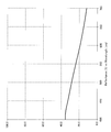
- FIG. 15 is a simulation result of the light reflectance of the insulating protective layer (three-layer structure: no thickness setting) for the TFT of Comparative Example 1.
- FIG. 16 is a simulation result of the light reflectivity of the insulating protective layer (two-layer structure: with thickness setting) for the TFT of Comparative Example 2.
- the light reflectance of the insulating protective layer was less than 50% with respect to light having a wavelength of 400 nm or more and 450 nm or less.
- the light reflectance of the insulating protective layer was 50% or more for light having a wavelength of 400 nm to 450 nm. Further, as shown in FIG. 7 to FIG. 10, it was found that the light reflectance at wavelengths of 400 nm or more and 450 nm or less increases as the number of three, four, six, eight, and insulating protective layers increases. . In particular, in the case of 8 layers, the light reflectivity is nearly 100%, and it was found that the light reflectivity cannot be increased even if the number of layers is increased further (saturation of light reflectivity). Therefore, it was found that the number of layers is preferably 8 or less from the viewpoint of saturation of the light reflectance and the viewpoint of reducing the manufacturing cost.
- the rate was 50% or more for light having a wavelength of 400 nm to 450 nm.
- the TFT of Example 7 has a slightly higher light reflectivity at a wavelength of 400 nm to 450 nm than the TFT of Example 2. This means that the light reflectance is higher when the thickness of the insulating protective layer is set at a plurality of wavelengths such as a wavelength of 400 nm and a wavelength of 450 nm than when the thickness of the insulating protective layer is set only at the wavelength of 430 nm.
- the operational stability ( ⁇ Vth) at the time of light irradiation of the TFTs according to Examples 1 to 3 and Comparative Examples 1 and 2 was evaluated.
- the element size of the TFT is a channel length of 180 ⁇ m and a channel width of 1 mm, respectively.
- Each TFT was left in the atmosphere for 1 hour in a dark environment to eliminate the influence of room light in the TFT storage environment.
- Each TFT was irradiated with light from the protective layer side with no voltage applied between the gate electrode and the source / drain electrodes (a xenon lamp was spectroscopically 10 ⁇ W / cm 2 ).
- the irradiation time was 10 minutes later, a voltage was applied between the gate electrode and the source / drain electrodes, and the Vg-Id characteristics were measured (at this time, the light irradiation was continued and the measurement wavelength was between 400 nm and 500 nm every 20 nm. ).
- ⁇ Vth for each wavelength was calculated from Vth calculated from the Vg-Id characteristics when no light was irradiated in advance.
- a semiconductor parameter analyzer manufactured by Agilent Technologies was used for measurement of the Vg-Id characteristics.
- Example 9 In Example 9, a TFT of the same type as the TFT 10 shown in FIG. 1 was produced.
- the TFT of Example 9 has an insulating protection with a 10-layer structure in which SiO x layers (thickness: 73.40 nm) and Nb 2 O y layers (thickness: 44.10 nm) are alternately stacked in order from the oxide semiconductor layer side. It was produced by the same method as in Example 2 except that the layer was formed. Note that the absolute refractive index (2.10) of the oxide semiconductor layer is “high”, and the relationship between the absolute refractive index and the previous layer of each of the insulating protective layers is “low” in order from the first layer. “High” is alternated.
- Example 10 a TFT of the same type as the TFT 10 shown in FIG. 1 was produced.
- the TFT of Example 10 has an 11-layer insulating protection in which SiO x layers (thickness: 73.40 nm) and Nb 2 O y layers (thickness: 44.10 nm) are alternately stacked in order from the oxide semiconductor layer side. It was produced by the same method as in Example 1 except that the layer was formed. Note that the absolute refractive index (2.10) of the oxide semiconductor layer is “high”, and the relationship between the absolute refractive index and the previous layer of each of the insulating protective layers is “low” in order from the first layer. “High” is alternated.
- FIGS. 18 and 19 are simulation results of the light reflectance of the insulating protective layer for the TFTs of Examples 9 and 10, respectively. From the simulation results shown in FIG. 18 and FIG. 19, it was found that the TFTs of Examples 9 and 10 have a high light reflectance with respect to light having a wavelength of 400 nm or more and 450 nm or less.
Landscapes
- Physics & Mathematics (AREA)
- Thin Film Transistor (AREA)
- Solid State Image Pick-Up Elements (AREA)
- Devices For Indicating Variable Information By Combining Individual Elements (AREA)
- Liquid Crystal (AREA)
- Nonlinear Science (AREA)
- Engineering & Computer Science (AREA)
- Microelectronics & Electronic Packaging (AREA)
- Mathematical Physics (AREA)
- Chemical & Material Sciences (AREA)
- Crystallography & Structural Chemistry (AREA)
- General Physics & Mathematics (AREA)
- Optics & Photonics (AREA)
Abstract
In,Zn,Ga及びSnからなる群から選ばれる少なくとも1種を含む酸化物半導体層と、酸化物半導体層を介して導通可能な一対の電極と、酸化物半導体層に積層された3層以上の積層構造を有し、酸化物半導体層と隣接する1層目24(1)は酸化物半導体層よりも絶対屈折率が低く、2層目24(2)は1層目24(1)よりも絶対屈折率が高く、且つ、2層目以降の各層はその前の層との絶対屈折率の高低関係が交互に異なり、1層目24(1)を含む各層の厚みをd(k)(nm)とし(k:酸化物半導体層側からの積層の順番)、各層の絶対屈折率をn(k)としたとき、400(nm)/4n(k)≦d(k)(nm)≦450(nm)/4n(k)を満たす絶縁保護層と、を有する酸化物半導体素子、酸化物半導体素子の製造方法及びその応用。
Description
本発明は、酸化物半導体素子、酸化物半導体素子の製造方法、表示装置、イメージセンサ及びX線センサに関する。
近年、In-Ga-Zn-O系の酸化物半導体薄膜を酸化物半導体層(チャネル層)に用いた酸化物半導体素子、特に薄膜トランジスタ(Thin Film Transistor : TFT)の研究開発が盛んである。酸化物半導体薄膜は低温成膜が可能であり、且つアモルファスシリコンよりも高移動度を示し、更に可視光に透明であることから、プラスチック板やフィルム等の基板上にフレキシブルなTFTを形成することが可能である。
しかしながら、実用化に向けてLCD(Liquid Crystal Display)や有機ELディスプレイ等の駆動回路に上記TFTを使用する場合には、TFT駆動時の動作不安定性(ΔVth:閾値シフト)や光照射時の動作不安定性が問題となる。
TFT駆動時の動作不安定性については、In-Ga-Zn-O系の酸化物が水分や酸素、汚染等に対して耐性が低いため、In-Ga-Zn-O系の酸化物を主体とした酸化物半導体層が大気中に露出していると当該酸化物が経年劣化してしまうことに起因する。
また、光照射時の動作不安定性については、以下の事に起因する。すなわち、LCDのバックライトや有機ELの青色発光層はλ=450nm程度の発光ピークを持ち、発光スペクトルの裾が420nmまで続いている。そして、これらの光が照射されるIn-Ga-Zn-O系等、In,Zn,Ga及びSnから選ばれる少なくとも1種を含む酸化物半導体層が、一般的に、可視光短波長領域の光(波長400nm以上450nm以下の光)に対して弱いことに起因する。
そこで、特開2009-141002号公報には、In-Ga-Zn-O系の酸化物を主体とした酸化物半導体層の露出面上に、SiOx層、SiNp層、SiOmNn層からなる三層構造の保護層を形成して、酸化物半導体層を水分等から保護することが開示されている。なお、上記x、m、nは、酸素不定比量であり、Pは窒素不定比量である。
また、国際公開第2009/075281号には、In-Ga-Zn-O系の酸化物を主体とした酸化物半導体層を保護する保護層上に、波長500nm以下の領域に大きな吸収又は反射を持つ樹脂材料や金属材料で構成された遮光膜を設けたTFTが開示されている。
しかしながら、特開2009-141002号公報のTFTでは、保護層を単に三層構造としているだけで、光照射時の動作不安定性については改善されていない。
また、国際公開第2009/075281号のTFTでは、遮光膜として光を吸収する樹脂材料を用いると、遮光膜に熱が発生してTFTの動作に影響を与えてしまう。また、遮光膜として光を反射する金属材料を用いると、ソース・ドレイン電極等の電極と導通しないこと等を考慮しなければならない。
本発明は上記事情に鑑みてなされたものであり、光照射時の動作安定性を確保すると共に、光照射による熱の発生を抑制する絶縁保護層を有した酸化物半導体素子及び酸化物半導体素子の製造方法を提供することを目的とする。
本発明の上記課題は下記の手段によって解決された。
<1>In,Zn,Ga及びSnからなる群から選ばれる少なくとも1種を含む酸化物半導体層と、酸化物半導体層を介して導通可能な一対の電極と、酸化物半導体層に積層された3層以上の積層構造を有し、酸化物半導体層と隣接する1層目は酸化物半導体層よりも絶対屈折率が低く、酸化物半導体層側からの積層順で2層目は1層目よりも絶対屈折率が高く、且つ、2層目以降のそれぞれの層はその前の層との絶対屈折率の高低関係が交互に異なり、1層目以降の各層の厚みをd(k)(nm)とし(k:酸化物半導体層側からの積層の順番)、各層の絶対屈折率をn(k)としたとき、400(nm)/4n(k)≦d(k)(nm)≦450(nm)/4n(k)を満たす絶縁保護層と、を有する酸化物半導体素子。
<1>In,Zn,Ga及びSnからなる群から選ばれる少なくとも1種を含む酸化物半導体層と、酸化物半導体層を介して導通可能な一対の電極と、酸化物半導体層に積層された3層以上の積層構造を有し、酸化物半導体層と隣接する1層目は酸化物半導体層よりも絶対屈折率が低く、酸化物半導体層側からの積層順で2層目は1層目よりも絶対屈折率が高く、且つ、2層目以降のそれぞれの層はその前の層との絶対屈折率の高低関係が交互に異なり、1層目以降の各層の厚みをd(k)(nm)とし(k:酸化物半導体層側からの積層の順番)、各層の絶対屈折率をn(k)としたとき、400(nm)/4n(k)≦d(k)(nm)≦450(nm)/4n(k)を満たす絶縁保護層と、を有する酸化物半導体素子。
<2>絶縁保護層の積層構造の層数は、4以上の偶数である、<1>に記載の酸化物半導体素子。
<3>絶縁保護層の積層構造の層数は、8以下である、<1>又は<2>に記載の酸化物半導体素子。
<4>絶縁保護層の積層構造の奇数番目の各層は、互いに同じ材料で構成され、絶縁保護層の積層構造の偶数番目の各層も、互いに同じ材料で構成されている、<1>~<3>の何れか1つに記載の酸化物半導体素子。
<5>絶縁保護層の各層のうち少なくとも2層の厚みd(k)は、波長400nm以上450nm以下の波長λのうち互いに異なる波長に基づいてd(k)=λ/4n(k)で表される厚みに設定されている、<1>~<4>の何れか1つに記載の酸化物半導体素子。
<6>絶縁保護層は、Hf,Ti,Nb,Zr,及びYからなる群から選ばれる何れか1つの酸化物層と、SiOx層(xは酸素不定比量)と、を有する、<1>~<5>の何れか1つに記載の酸化物半導体素子。
<7>絶縁保護層は、酸化物半導体層側から順に、SiOx層(xは酸素不定比量)と、Nb2Oy層(yは酸素不定比量)とが交互に積層された積層構造を有する、<1>~<6>の何れか1つに記載の酸化物半導体素子。
<8><1>~<7>の何れか1つに記載の酸化物半導体素子の製造方法であって、絶縁保護層の形成時又は形成後に、300℃以下で熱処理する工程を含む、酸化物半導体素子の製造方法。
<9>絶縁保護層の各層は、スパッタリング法で形成する、<8>に記載の酸化物半導体素子の製造方法。
<10>酸化物半導体層の絶縁保護層が配置されている側とは反対側にゲート絶縁層を介して配置されたゲート電極を有する薄膜トランジスタである、<1>~<7>の何れか1つに記載の酸化物半導体素子。
<11><10>に記載の酸化物半導体素子を備えた表示装置。
<12><10>に記載の酸化物半導体素子を備えたイメージセンサ。
<13><10>に記載の酸化物半導体素子を備えたX線センサ。
本発明によれば、絶縁保護層により、光照射時の動作安定性が確保されると共に、光照射による熱の発生が抑制される。
以下、添付の図面を参照しながら、本発明の実施形態に係る酸化物半導体素子及び酸化物半導体素子の製造方法について具体的に説明する。なお、図中、同一又は対応する機能を有する部材(構成要素)には同じ符号を付して適宜説明を省略する。また、以下で説明する場合に用いる「上」及び「下」という用語は、便宜的に用いるものであって、方向に拘束されるべきでない。
1.酸化物半導体素子:薄膜トランジスタの概略構成
本発明の実施形態に係る酸化物半導体素子は、薄膜トランジスタ:TFTやフォトダイオード等である。以下では、酸化物半導体素子としてTFTを一例に挙げて説明する。
本発明の実施形態に係る酸化物半導体素子は、薄膜トランジスタ:TFTやフォトダイオード等である。以下では、酸化物半導体素子としてTFTを一例に挙げて説明する。
TFTは、少なくとも、ゲート電極、ゲート絶縁層、酸化物半導体層、ソース電極及びドレイン電極を有し、ゲート電極に電圧を印加して、酸化物半導体層に流れる電流を制御し、ソース電極とドレイン電極間の電流をスイッチングする機能を有するアクテイブ素子である。
TFTの素子構造としては、ゲート電極の位置に基づいた、いわゆる逆スタガ構造(ボトムゲート型とも呼ばれる)及びスタガ構造(トップゲート型とも呼ばれる)があるが、本実施形態では、逆スタガ構造が用いられる。
また、酸化物半導体層とソース電極及びドレイン電極(適宜、「ソース・ドレイン電極」という。)との接触部分に基づき、いわゆるトップコンタクト型、ボトムコンタクト型のいずれの態様であってもよい。
なお、トップゲート型とは、TFTが形成されている基板を最下層としたときに、ゲート絶縁層の上側にゲート電極が配置され、ゲート絶縁層の下側に酸化物半導体層が形成された形態であり、ボトムゲート型とは、ゲート絶縁層の下側にゲート電極が配置され、ゲート絶縁層の上側に酸化物半導体層が形成された形態である。また、ボトムコンタクト型とは、TFTが形成されている基板を最下層としたときに、ソース・ドレイン電極が酸化物半導体層よりも先に形成されて酸化物半導体層の下面がソース・ドレイン電極に接触する形態であり、トップコンタクト型とは、酸化物半導体層がソース・ドレイン電極よりも先に形成されて酸化物半導体層の上面がソース・ドレイン電極に接触する形態である。
また、酸化物半導体層とソース電極及びドレイン電極(適宜、「ソース・ドレイン電極」という。)との接触部分に基づき、いわゆるトップコンタクト型、ボトムコンタクト型のいずれの態様であってもよい。
なお、トップゲート型とは、TFTが形成されている基板を最下層としたときに、ゲート絶縁層の上側にゲート電極が配置され、ゲート絶縁層の下側に酸化物半導体層が形成された形態であり、ボトムゲート型とは、ゲート絶縁層の下側にゲート電極が配置され、ゲート絶縁層の上側に酸化物半導体層が形成された形態である。また、ボトムコンタクト型とは、TFTが形成されている基板を最下層としたときに、ソース・ドレイン電極が酸化物半導体層よりも先に形成されて酸化物半導体層の下面がソース・ドレイン電極に接触する形態であり、トップコンタクト型とは、酸化物半導体層がソース・ドレイン電極よりも先に形成されて酸化物半導体層の上面がソース・ドレイン電極に接触する形態である。
図1は、本発明の実施形態に係るTFTであって、ボトムゲート構造でトップコンタクト型のTFTの一例を示す模式図である。
図1に示すTFT10は、基板12の一方の主面上に形成されたゲート電極14と、このゲート電極14を覆うゲート絶縁層16と、このゲート絶縁層16のゲート電極14が配置されている側とは反対側に配置された酸化物半導体層18と、を有している。さらに、TFT10は、酸化物半導体層18のゲート絶縁層16が配置されている側と反対側に互いに離間して配置されたソース電極20及びドレイン電極22と、これらソース・ドレイン電極20,22との間から露出する酸化物半導体層18の表面上に積層された絶縁保護層24とを有している。
そして、本例では絶縁保護層24が、酸化物半導体層18側から、1層目24(1)、2層目24(2)、・・・k層目24(k)(k:3以上の整数)まで有する、すなわち、3層以上の積層構造とされている。
そして、本例では絶縁保護層24が、酸化物半導体層18側から、1層目24(1)、2層目24(2)、・・・k層目24(k)(k:3以上の整数)まで有する、すなわち、3層以上の積層構造とされている。
図2は、本発明の実施形態に係るTFTであって、ボトムゲート構造でボトムコンタクト型のTFTの一例を示す模式図である。
図2に示すTFT30は、基板12の一方の主面上にゲート電極14と、ゲート絶縁層16と、が順に積層されている。このゲート絶縁層16の表面上には、ソース電極20及びドレイン電極22が互いに離間して設置され、これらの上には酸化物半導体層18が積層されている。さらに、TFT30は、酸化物半導体層18の露出面上に積層され、3層以上の積層構造とされた絶縁保護層24を有している。
なお、本実施形態に係るTFTは、上記以外にも、様々な構成をとることが可能であり、例えば基板12上に絶縁層を設けたり、酸化物半導体層18を複数層にしたり、酸化物半導体層18とソース・ドレイン電極20,22との間にコンタクト層を設けたりする構成であってもよい。
以下、TFT10及びTFT30の各構成要素について詳述する。
<TFTの詳細構成>
-基板-
基板12の形状、構造、大きさ等については、膜を成膜可能な主面があることを前提として特に制限はなく、目的に応じて適宜選択することが出来る。基板12の構造は単層構造であってもよいし、積層構造であってもよい。
-基板-
基板12の形状、構造、大きさ等については、膜を成膜可能な主面があることを前提として特に制限はなく、目的に応じて適宜選択することが出来る。基板12の構造は単層構造であってもよいし、積層構造であってもよい。
基板12の材質としては特に限定はなく、例えばガラス、YSZ(イットリウム安定化ジルコニウム)等の無機基板、樹脂基板や、その複合材料等を用いることが出来る。中でも軽量である点、可撓性を有する点から樹脂基板やその複合材料が好ましい。具体的には、ポリブチレンテレフタレート、ポリエチレンテレフタレート、ポリエチレンナフタレート、ポリブチレンナフタレート、ポリスチレン、ポリカーボネート、ポリスルホン、ポリエーテルスルホン、ポリアリレート、アリルジグリコールカーボネート、ポリアミド、ポリイミド、ポリアミドイミド、ポリエーテルイミド、ポリベンズアゾール、ポリフェニレンサルファイド、ポリシクロオレフィン、ノルボルネン樹脂、ポリクロロトリフルオロエチレン等のフッ素樹脂、液晶ポリマー、アクリル樹脂、エポキシ樹脂、シリコン樹脂、アイオノマー樹脂、シアネート樹脂、架橋フマル酸ジエステル、環状ポリオレフィン、芳香族エーテル、マレイミドーオレフィン、セルロース、エピスルフィド化合物等の合成樹脂基板、酸化珪素粒子との複合プラスチック材料、金属ナノ粒子、無機酸化物ナノ粒子、無機窒化物ナノ粒子等との複合プラスチック材料、カーボン繊維、カーボンナノチューブとの複合プラスチック材料、ガラスフェレーク、ガラスファイバー、ガラスビーズとの複合プラスチック材料、粘土鉱物や雲母派生結晶構造を有する粒子との複合プラスチック材料、薄いガラスと上記単独有機材料との間に少なくとも1回の接合界面を有する積層プラスチック材料、無機層と有機層を交互に積層することで、少なくとも1回以上の接合界面を有するバリア性能を有する複合材料、ステンレス基板或いはステンレスと異種金属を積層した金属多層基板、アルミニウム基板或いは表面に酸化処理(例えば陽極酸化処理)を施すことで表面の絶縁性を向上させた酸化皮膜付きのアルミニウム基板等を用いることが出来る。また、樹脂基板は、耐熱性、寸法安定性、耐溶剤性、電気絶縁性、加工性、低通気性、又は低吸湿性等に優れていることが好ましい。樹脂基板は、水分や酸素の透過を防止するためのガスバリア層や、樹脂基板の平坦性や下部電極との密着性を向上するためのアンダーコート層等を備えることが好ましい。ここで、アンダーコート層を樹脂基板の片面に形成した場合には、内部残留応力にて樹脂基板に反りが生じるため、両面にコートするかもしくは、低応力に制御した膜質、または積層にて圧縮/引張応力にて制御した方が好ましい。また、アンダーコート層は、バリア性を高めるため、後述するゲート絶縁層16などに用いられる材料が好ましい。
-ゲート電極-
ゲート電極14は、基板12の一方の主面上に形成されている。
ゲート電極14は、基板12の一方の主面上に形成されている。
ゲート電極14を構成する導電膜は、高い導電性を有するものを用いることが好ましく、例えばAl,Mo,Cr,Ta,Ti,Au,Au等の金属膜や、Al-Nd、Ag合金、酸化錫、酸化亜鉛、酸化インジウム、酸化インジウム錫(ITO)、酸化亜鉛インジウム(IZO)等の金属酸化物導電膜等を用いることができる。
-ゲート絶縁層-
ゲート絶縁層16は、ゲート電極14を覆うように、基板12とは反対側のゲート電極14の表面上と、基板12の露出面上に積層されている。
ゲート絶縁層16は、ゲート電極14を覆うように、基板12とは反対側のゲート電極14の表面上と、基板12の露出面上に積層されている。
ゲート絶縁層16を構成する絶縁膜は、高い絶縁性を有するものが好ましく、例えばSiOx,SiNp,SiON,Al2O3,Y2O3,Ta2O5,HfO2等の絶縁膜、又はこれらの化合物を少なくとも二つ以上含む絶縁膜としてもよい。
-酸化物半導体層-
酸化物半導体層18は、ゲート電極14とは反対側のゲート絶縁層16の表面上に積層されている。
酸化物半導体層18は、ゲート電極14とは反対側のゲート絶縁層16の表面上に積層されている。
酸化物半導体層18は、In,Zn,Ga及びSnから選ばれる少なくとも1種を含む酸化物半導体を主体としていればよく、その他に不純物等を含有していても良い。ここで、「主体」とは、酸化物半導体層18を構成する構成成分のうち、最も多く含有されている成分を表す。
酸化物半導体は、非晶質又は結晶質のいずれであってもよいが、好ましくは、非晶質酸化物半導体が用いられる。半導体膜を酸化物半導体により構成すれば、非晶質シリコンの半導体膜に比べて電荷の移動度がはるかに高く、低電圧で駆動させることができる。また、酸化物半導体を用いれば、通常、シリコンよりも光透過性が高い半導体膜を形成することができる。また、酸化物半導体、特に非晶質酸化物半導体は、低温(例えば室温)で均一に成膜が可能であるため、プラスチックのような可撓性のある樹脂基板を用いるときに特に有利となる。
酸化物半導体は、非晶質又は結晶質のいずれであってもよいが、好ましくは、非晶質酸化物半導体が用いられる。半導体膜を酸化物半導体により構成すれば、非晶質シリコンの半導体膜に比べて電荷の移動度がはるかに高く、低電圧で駆動させることができる。また、酸化物半導体を用いれば、通常、シリコンよりも光透過性が高い半導体膜を形成することができる。また、酸化物半導体、特に非晶質酸化物半導体は、低温(例えば室温)で均一に成膜が可能であるため、プラスチックのような可撓性のある樹脂基板を用いるときに特に有利となる。
酸化物半導体の構成材料としては、In,Zn,Ga及びSnから選ばれる少なくとも1種を含んでいれば、特に限定されることはないが、In、Ga及びZnのうちの少なくとも1種を含む酸化物(例えばIn-O系)が好ましい。特に、In、Ga及びZnのうちの少なくとも2種を含む酸化物(例えばIn-Zn-O系、In-Ga-O系、Ga-Zn-O系)が好ましく、In、Ga及びZnを全て含む酸化物がより好ましい。In-Ga-Zn-O系酸化物半導体としては、結晶状態における組成がInGaO3(ZnO)m(mは6未満の自然数)で表される酸化物半導体が好ましく、特に、InGaZnO4がより好ましい。この組成の酸化物半導体の特徴としては、電気伝導度が増加するにつれ、電子移動度が増加する傾向を示す。ただし、In-Ga-Zn-O系の組成比は、厳密にIn:Ga:Zn=1:1:1となる必要はない。
酸化物半導体層18の層構造は、2層以上から構成されていても良く、酸化物半導体層18が低抵抗層と高抵抗層より形成され、低抵抗層がゲート絶縁層16と接し、高抵抗層がソース電極20及びドレイン電極22の少なくとも一方と電気的に接していることが好ましい。
酸化物半導体層18の厚みは、特に限定されないが、キャリア移動の確保及びコストの抑制という両者の観点から、30nm以上60nm以下であることがより好ましい。
-ソース・ドレイン電極-
ソース・ドレイン電極20,22は、ゲート絶縁層16とは反対側の酸化物半導体層18の表面上に互いに間隔をあけて形成されており、ゲート電極14の印加電圧によって酸化物半導体層18と導通可能になっている。
ソース・ドレイン電極20,22は、ゲート絶縁層16とは反対側の酸化物半導体層18の表面上に互いに間隔をあけて形成されており、ゲート電極14の印加電圧によって酸化物半導体層18と導通可能になっている。
ソース・ドレイン電極20,22を構成する導電膜は、高い導電性を有するものを用い、例えばAl,Mo,Cr,Ta,Ti,Au,Au等の金属膜、Al-Nd、Ag合金、酸化錫、酸化亜鉛、酸化インジウム、酸化インジウム錫(ITO)、酸化亜鉛インジウム(IZO)等の金属酸化物導電膜等を用いて形成することが出来る。ソース・ドレイン電極20,22としてはこれらの導電膜を単層構造又は2層以上の積層構造として用いることができる。
-絶縁保護層-
TFT10及びTFT30の絶縁保護層24は、ソース・ドレイン電極20,22との間から露出する酸化物半導体層18上に積層され、酸化物半導体層18を水や酸素等から絶縁保護している。
TFT10及びTFT30の絶縁保護層24は、ソース・ドレイン電極20,22との間から露出する酸化物半導体層18上に積層され、酸化物半導体層18を水や酸素等から絶縁保護している。
絶縁保護層24において、酸化物半導体層18と隣接する1層目24(1)は、酸化物半導体層18よりも絶対屈折率が低い。また、酸化物半導体層18側からの積層順で、2層目24(2)以降の各層24(2)、・・・24(k)はその前の層との絶対屈折率の高低関係が交互に異なっている。具体的に、酸化物半導体層18の絶対屈折率(InGaZnO4の場合、波長400nm以上450以下の範囲で約2.11~2.10の絶対屈折率)を「高」として、一層目24(1)から順に、「低」、「高」、「低」、「高」・・・・となっている。絶対屈折率の高低関係の順が逆であると、絶縁保護層24の外側(基板12とは反対側)から酸化物半導体層18側に入射する光の反射率が著しく低くなるからである。
尚、絶縁保護層の1層目24(1)からk層目24(k)の各層における絶対屈折率は、酸化物半導体層18側からの積層順で、2S(Sは自然数)番目の層の絶対屈折率をn(2S)とし、これに隣接する層の絶対屈折率をそれぞれn(2S-1)、n(2S+1)とすると、次の関係式で表される。
n(2S-1)<n(2S)>n(2S+1)
尚、絶縁保護層の1層目24(1)からk層目24(k)の各層における絶対屈折率は、酸化物半導体層18側からの積層順で、2S(Sは自然数)番目の層の絶対屈折率をn(2S)とし、これに隣接する層の絶対屈折率をそれぞれn(2S-1)、n(2S+1)とすると、次の関係式で表される。
n(2S-1)<n(2S)>n(2S+1)
また、絶縁保護層24において、各層24(1)、24(2)、・・・24(k)の厚みは、その厚みをd(k)とし(k:酸化物半導体層18側からの積層の順番)、波長400nm以上450nm以下の任意の波長をλとし、各層の絶対屈折率をn(k)としたとき、d(k)=λ/4n(k)で表される厚みとなるように設定され、400(nm)/4n(k)≦d(k)(nm)≦450(nm)/4n(k)を満たしている。
例えば、絶縁保護層24における各層の厚みを設定する際の波長光λを430nmとした場合、各層の厚みd(k)は430(nm)/4n(k)で表される厚みとなることを目標とするが、必ずしもd(k)=430(nm)/4n(k)を満たす必要はなく、d(k)=λ/4n(k)(400nm≦λ≦450nm)、すなわち、400(nm)/4n(k)≦d(k)(nm)≦450(nm)/4n(k)を満たす厚さであればよい。
例えば、絶縁保護層24における各層の厚みを設定する際の波長光λを430nmとした場合、各層の厚みd(k)は430(nm)/4n(k)で表される厚みとなることを目標とするが、必ずしもd(k)=430(nm)/4n(k)を満たす必要はなく、d(k)=λ/4n(k)(400nm≦λ≦450nm)、すなわち、400(nm)/4n(k)≦d(k)(nm)≦450(nm)/4n(k)を満たす厚さであればよい。
これにより、本実施形態に係るTFT10,30では、保護層24の外側(基板12とは反対側)から酸化物半導体層18側に向かって波長400nm以上450nm以下の光が入射しても、絶縁保護層24の各層24(1)、24(2)、・・・24(k)の界面で反射されるので、酸化物半導体層18に当たる光量が抑制される。したがって、酸化物半導体層18がIn,Zn,Ga及びSnから選ばれる少なくとも1種を含んでいて波長400nm以上450nm以下の光に弱くても(TFTの動作不安定を起こすものであっても)、酸化物半導体層18に当たる光量が抑制されるため、TFT10,30の光照射時の動作安定性を確保することができる。
また、絶縁保護層24は、光を反射するので、光を吸収する場合に比べて、光照射による熱の発生を抑制することができる。
また、絶縁保護層24は、光を反射するので、光を吸収する場合に比べて、光照射による熱の発生を抑制することができる。
上記各層の24(1)、24(2)、・・・24(k)の厚みd(k)は、それぞれ、波長400nm以上450nm以下の波長のうち互いに同じ波長に基づいて設定されてもよいが、異なる波長に基づいて設定されていることが好ましい。複数の波長を有した光を反射するようになり、酸化物半導体層18に当たる光量がより抑制されるからである。
なお、厚みd(k)が互いに異なる波長を用いて表される場合は、各層24(1)、24(2)、・・・24(k)のうち少なくとも2層の厚みd(k)が、波長400nm以上450nm以下の波長のうち互いに異なる波長を用いて表されていればよい。例えば、奇数番目の各層の厚みが波長400nmで表され、偶数番目の各層の厚みが波長450nmで表されていればよい。
なお、厚みd(k)が互いに異なる波長を用いて表される場合は、各層24(1)、24(2)、・・・24(k)のうち少なくとも2層の厚みd(k)が、波長400nm以上450nm以下の波長のうち互いに異なる波長を用いて表されていればよい。例えば、奇数番目の各層の厚みが波長400nmで表され、偶数番目の各層の厚みが波長450nmで表されていればよい。
なお、積層構造の層数は、3以上とされている。3未満だと、例え各層24(1)、24(2)、・・・24(k)の厚みがd(k)=λ/4n(k)で表されても光反射率が50%を下回り、光照射時の動作安定性を確保することが難しいからである。
また、積層構造の層数は、4以上の偶数であることが好ましい。4以上の偶数だと、TFT10,30が後述する液晶表示装置等に用いられたときに、絶縁保護層24の上に積層される層間絶縁層に用いられる材料(SiOxがよく用いられる)と、後述する絶縁保護層24の最終層目24(k)(k=絶縁保護層24の層数)に用いられる材料とが相違し易く、最終層目24(k)の界面における反射を確保することができる。
さらに、例えば絶縁保護層24の各層24(1)、24(2)、・・・24(k)の互いに隣接する層間の絶対屈折率の差が1以上の場合(材料の組み合わせでは例えばSiOxとN2Oyの組み合わせ)、積層構造の層数は、8以下であることが好ましい。8以下だと光反射率が100%近くまで高くでき(8以上だと飽和)、且つ、製造コストを抑えることができるからである。
また、積層構造の層数は、4以上の偶数であることが好ましい。4以上の偶数だと、TFT10,30が後述する液晶表示装置等に用いられたときに、絶縁保護層24の上に積層される層間絶縁層に用いられる材料(SiOxがよく用いられる)と、後述する絶縁保護層24の最終層目24(k)(k=絶縁保護層24の層数)に用いられる材料とが相違し易く、最終層目24(k)の界面における反射を確保することができる。
さらに、例えば絶縁保護層24の各層24(1)、24(2)、・・・24(k)の互いに隣接する層間の絶対屈折率の差が1以上の場合(材料の組み合わせでは例えばSiOxとN2Oyの組み合わせ)、積層構造の層数は、8以下であることが好ましい。8以下だと光反射率が100%近くまで高くでき(8以上だと飽和)、且つ、製造コストを抑えることができるからである。
各層24(1)、24(2)、・・・24(k)のうち奇数番目の各層は、互いに同じ材料で構成されても異なる材料で構成されてもよいが、製造コストを抑制するという観点から、互いに同じ材料で構成されていることが好ましい。同様に、各層24(1)、24(2)、・・・24(k)のうち偶数番目の各層は、互いに同じ材料で構成されても異なる材料で構成されてもよいが、製造コストを抑制するという観点から、互いに同じ材料で構成されていることが好ましい。
絶縁保護層24の材料としては、酸化物や窒化物等の絶縁材料を用いることができる。酸化物としては、Hf,Ti,Nb,Zr,Si,及びYから選ばれる何れか1つの酸化物が挙げられる。具体的には、Y2O3,Ta2O5,HfO2等である。窒化物としては、SiNp,SiON等が挙げられる。
各層24(1)、24(2)、・・・24(k)のうち絶対屈折率が低い層に用いる材料としては、例えば、絶対屈折率が波長400nm以上450nm以下の範囲で約1.47~1.46のSiOx(xは酸素不定比量で2付近)等を用いることができる。なお、以降SiOxを主体とした層をSiOx層と略す。ここで、「主体」とは、層中のSiOxの量が90質量%を超えていることを意味する。
各層24(1)、24(2)、・・・24(k)のうち絶対屈折率が高い層に用いる材料としては、例えば、Hf,Ti,Nb,Zr,及びYから選ばれる1つの酸化物材料を用いることができる。具体的に、波長400nm以上450nm以下の範囲で絶対屈折率が約2.50~2.40のNb2Oy(yは酸素不定比量で5付近)を用いることができる。他にも、波長400nm以上450nm以下の範囲で絶対屈折率が約2.16~2.11のHfOe(eは酸素不定比量で2付近)や、波長400nm以上450nm以下の範囲で絶対屈折率が約2.26~2.23のTiOf(fは酸素不定比量で2付近)を用いることもできる。なお、以降Nb2Oyを主体とした層をNb2Oy層と略す。ここで、主体とは、層中のNb2Oyの量が90質量%を超えていることを意味する。
絶縁保護層24は、各層24(1)、24(2)、・・・24(k)のうち奇数番目が同じ材料で構成され、また偶数番目が同じ材料で構成する観点と、屈折率の高低が明確(高低の差が大きい)となるという観点から、酸化物半導体層18側から順に、SiOx層と、Nb2Oy層とが交互に積層された積層構造であることが好ましい。
2.酸化物半導体素子の製造方法:TFTの製造方法
次に、本実施形態に係る酸化物半導体素子の製造方法としてTFT10の製造方法を一例に挙げて説明する。
次に、本実施形態に係る酸化物半導体素子の製造方法としてTFT10の製造方法を一例に挙げて説明する。
-ゲート電極形成工程-
まず、ゲート電極形成工程を行う。このゲート電極形成工程では、基板12を用意する。そして、用意した基板12上に導電膜を成膜する。この成膜方法としては、印刷方式、コーティング方式等の湿式方式、真空蒸着法、スパッタリング法、イオンプレーティング法等の物理的方式、CVD(Chemical Vapor Deposition)、プラズマCVD法等の化学的方式等の中から使用する材料との適性を考慮した方法が用いられる。
まず、ゲート電極形成工程を行う。このゲート電極形成工程では、基板12を用意する。そして、用意した基板12上に導電膜を成膜する。この成膜方法としては、印刷方式、コーティング方式等の湿式方式、真空蒸着法、スパッタリング法、イオンプレーティング法等の物理的方式、CVD(Chemical Vapor Deposition)、プラズマCVD法等の化学的方式等の中から使用する材料との適性を考慮した方法が用いられる。
成膜後は、導電膜を、フォトリソグラフィー及びエッチング法又はリフトオフ法等により所定の形状にパターンニングすることにより、導電膜からゲート電極14を形成する。この際、ゲート電極14及びゲート配線を同時にパターンニングすることが好ましい。
-ゲート絶縁層形成工程、酸化物半導体層形成工程及び絶縁保護層形成工程-
次に、ゲート絶縁層形成工程、酸化物半導体層形成工程及び絶縁保護層形成工程を行う。これらの形成工程は、ゲート絶縁層形成工程、酸化物半導体層形成工程及び絶縁保護層形成工程と順番に行ってもよいが、同時に行ってもよく、また以下のように成膜だけ順番通りにし、パターニングは逆の順番にしてもよい。
次に、ゲート絶縁層形成工程、酸化物半導体層形成工程及び絶縁保護層形成工程を行う。これらの形成工程は、ゲート絶縁層形成工程、酸化物半導体層形成工程及び絶縁保護層形成工程と順番に行ってもよいが、同時に行ってもよく、また以下のように成膜だけ順番通りにし、パターニングは逆の順番にしてもよい。
これらの形成工程では、まず、ゲート電極14上及び基板12上に、絶縁膜、酸化物半導体膜、及び積層構造の絶縁膜を順次成膜する。
これらの成膜方法としては、印刷方式、コーティング方式等の湿式方式、真空蒸着法、スパッタリング法、イオンプレーティング法等の物理的方式、CVD、プラズマCVD法等の化学的方式等の中から使用する材料との適性を考慮した方法が用いられる。これらの中でも、膜厚の制御がし易いという観点から、真空蒸着法、スパッタリング法、イオンプレーティング法、CVD又はプラズマCVD法等の気相成膜法を用いるのが好ましい。気相成膜法の中でも、スパッタリング法、パルスレーザー蒸着法(PLD法)がより好ましい。さらに、量産性の観点から、スパッタリング法がさらに好ましい。例えば、RFマグネトロンスパッタリング成膜法により、真空度及び酸素流量を制御して成膜することができる。
なお、絶縁膜、酸化物半導体膜、及び積層構造の絶縁膜の成膜方法は、これらを連続的に成膜できる点で、同じであることが好ましい。
これらの成膜方法としては、印刷方式、コーティング方式等の湿式方式、真空蒸着法、スパッタリング法、イオンプレーティング法等の物理的方式、CVD、プラズマCVD法等の化学的方式等の中から使用する材料との適性を考慮した方法が用いられる。これらの中でも、膜厚の制御がし易いという観点から、真空蒸着法、スパッタリング法、イオンプレーティング法、CVD又はプラズマCVD法等の気相成膜法を用いるのが好ましい。気相成膜法の中でも、スパッタリング法、パルスレーザー蒸着法(PLD法)がより好ましい。さらに、量産性の観点から、スパッタリング法がさらに好ましい。例えば、RFマグネトロンスパッタリング成膜法により、真空度及び酸素流量を制御して成膜することができる。
なお、絶縁膜、酸化物半導体膜、及び積層構造の絶縁膜の成膜方法は、これらを連続的に成膜できる点で、同じであることが好ましい。
次に、積層構造の絶縁膜を、フォトリソグラフィー及びエッチング法又はリフトオフ法等により所定の形状にパターンニングする。これにより、積層構造の絶縁膜から、絶縁保護層24を形成する。
次に、酸化物半導体膜を、フォトリソグラフィー及びエッチング法又はリフトオフ法等により所定の形状にパターンニングする。これにより、酸化物半導体膜から酸化物半導体層18を形成する。
次に、絶縁膜を、フォトリソグラフィー及びエッチング法又はリフトオフ法等により所定の形状にパターンニングする。これにより、絶縁膜からゲート絶縁層16を形成する。
-ソース・ドレイン電極形成工程-
次に、導電膜を、フォトリソグラフィー及びエッチング法又はリフトオフ法等により所定の形状にパターンニングして、導電膜からソース・ドレイン電極20,22を形成する。
次に、導電膜を、フォトリソグラフィー及びエッチング法又はリフトオフ法等により所定の形状にパターンニングして、導電膜からソース・ドレイン電極20,22を形成する。
以上の工程を経ることにより、図1に示すTFT10を作製することができる。
なお、上記酸化物半導体膜の成膜後の何れかの工程では、熱処理工程を行ってもよい。本実施形態では、絶縁保護層24が光を反射することから、酸化物半導体膜(又は酸化物半導体層18)の酸素制御を考慮せずに、例えば、絶縁保護層24の形成時又は形成後、300℃以下の低温で熱処理することができる。これにより、フレキシブルな基板12の選択幅が広がる。
3.変形例
なお、本発明を特定の実施形態について詳細に説明したが、本発明はかかる実施形態に限定されるものではなく、本発明の範囲内にて他の種々の実施形態が可能であることは当業者にとって明らかである。
なお、本発明を特定の実施形態について詳細に説明したが、本発明はかかる実施形態に限定されるものではなく、本発明の範囲内にて他の種々の実施形態が可能であることは当業者にとって明らかである。
例えば、実施形態では、絶縁保護層24において、各層24(1)、24(2)、・・・24(k)の厚みd(k)は、波長400nm以上450nm以下の任意の波長をλとし、各層の絶対屈折率をn(k)としたとき、d(k)=λ/4n(k)で表される場合を説明した。しかしながら、絶縁保護層24には、上記各層の他に、波長400~450nm以外の他の波長で反射する他の層を追加することもできる。
4.応用
以上で説明した本実施形態に係るTFT10,30の用途には特に限定はないが、例えば電気光学装置(例えば液晶表示装置、有機EL(Electro Luminescence)表示装置、無機EL表示装置等の表示装置、等)における駆動素子、特に大面積デバイスに用いる場合に好適である。
さらに本実施形態のTFT10,30は、樹脂基板を用いた低温プロセスで作製可能なデバイスに特に好適であり(例えばフレキシブルディスプレイ等)、X線センサなどの各種センサ、MEMS(Micro Electro Mechanical System)等、種々の電子デバイスにおける駆動素子(駆動回路)として、好適に用いられるものである。
以上で説明した本実施形態に係るTFT10,30の用途には特に限定はないが、例えば電気光学装置(例えば液晶表示装置、有機EL(Electro Luminescence)表示装置、無機EL表示装置等の表示装置、等)における駆動素子、特に大面積デバイスに用いる場合に好適である。
さらに本実施形態のTFT10,30は、樹脂基板を用いた低温プロセスで作製可能なデバイスに特に好適であり(例えばフレキシブルディスプレイ等)、X線センサなどの各種センサ、MEMS(Micro Electro Mechanical System)等、種々の電子デバイスにおける駆動素子(駆動回路)として、好適に用いられるものである。
5.電気光学装置及びセンサ
本実施形態の電気光学装置又はセンサは、本実施形態に係るTFT10を備えて構成される。
電気光学装置の例としては、表示装置(例えば液晶表示装置、有機EL表示装置、無機EL表示装置、等)がある。
センサの例としては、CCD(Charge Coupled Device)又はCMOS(Complementary Metal Oxide Semiconductor)等のイメージセンサや、X線センサ等が好適である。
以下、本実施形態に係るTFT10を備えた電気光学装置又はセンサの代表例として、液晶表示装置、有機EL表示装置、X線センサについて説明する。
本実施形態の電気光学装置又はセンサは、本実施形態に係るTFT10を備えて構成される。
電気光学装置の例としては、表示装置(例えば液晶表示装置、有機EL表示装置、無機EL表示装置、等)がある。
センサの例としては、CCD(Charge Coupled Device)又はCMOS(Complementary Metal Oxide Semiconductor)等のイメージセンサや、X線センサ等が好適である。
以下、本実施形態に係るTFT10を備えた電気光学装置又はセンサの代表例として、液晶表示装置、有機EL表示装置、X線センサについて説明する。
6.液晶表示装置
図3に、本発明の電気光学装置の一実施形態の液晶表示装置について、その一部分の概略断面図を示し、図4にその電気配線の概略構成図を示す。
図3に、本発明の電気光学装置の一実施形態の液晶表示装置について、その一部分の概略断面図を示し、図4にその電気配線の概略構成図を示す。
図3に示すように、本実施形態の液晶表示装置100は、図1に示したボトムゲート構造でトップコンタクト型のTFT10と、TFT10のパッシベーション層102で保護された酸化物半導体層18上に画素下部電極104およびその対向上部電極106で挟まれた液晶層108と、各画素に対応させて異なる色を発色させるためのRGBカラーフィルタ110とを備え、TFT10の基板12側およびRGBカラーフィルタ110上にそれぞれ偏光板112a、112bを備えた構成である。
また、図4に示すように、本実施形態の液晶表示装置100は、互いに平行な複数のゲート配線112と、該ゲート配線112と交差する、互いに平行なデータ配線114とを備えている。ここでゲート配線112とデータ配線114は電気的に絶縁されている。ゲート配線112とデータ配線114との交差部付近に、TFT10が備えられている。
TFT10のゲート電極14は、ゲート配線112に接続されており、TFT10のソース電極20はデータ配線114に接続されている。また、TFT10のドレイン電極22はゲート絶縁層16に設けられたコンタクトホール116を介して(コンタクトホール116に導電体が埋め込まれて)画素下部電極104に接続されている。この画素下部電極104は、接地された対向上部電極106とともにキャパシタ118を構成している。
このような液晶表示装置100は、波長400nm以上450nm以下の光を含むバックライトがTFT10の保護層24の外側(基板12とは反対側)から酸化物半導体層18側に向かって照射される。
本実施形態のTFT10では、酸化物半導体層18側に向かうバックライトが絶縁保護層24で反射されるので、酸化物半導体層18に当たる光量が抑制される。したがって、酸化物半導体層18がIn,Zn,Ga及びSnから選ばれる少なくとも1種を含んでいて波長400nm以上450nm以下の光に弱くても、酸化物半導体層18に当たる光量が抑制されるため、TFT10の光照射時の動作安定性を確保することができる。このため、液晶表示装置100の信頼性が増す。
本実施形態のTFT10では、酸化物半導体層18側に向かうバックライトが絶縁保護層24で反射されるので、酸化物半導体層18に当たる光量が抑制される。したがって、酸化物半導体層18がIn,Zn,Ga及びSnから選ばれる少なくとも1種を含んでいて波長400nm以上450nm以下の光に弱くても、酸化物半導体層18に当たる光量が抑制されるため、TFT10の光照射時の動作安定性を確保することができる。このため、液晶表示装置100の信頼性が増す。
7.有機EL表示装置
図5に、本発明の電気光学装置の一実施形態のアクティブマトリックス方式の有機EL表示装置について、その一部分の概略断面図を示し、図6に電気配線の概略構成図を示す。
図5に、本発明の電気光学装置の一実施形態のアクティブマトリックス方式の有機EL表示装置について、その一部分の概略断面図を示し、図6に電気配線の概略構成図を示す。
有機EL表示装置の駆動方式には、単純マトリックス方式とアクティブマトリックス方式の2種類がある。単純マトリックス方式は低コストで作製できるメリットがあるが、走査線を1本ずつ選択して画素を発光させることから、走査線数と走査線あたりの発光時間は反比例する。そのため高精細化、大画面化が困難となっている。アクティブマトリックス方式は画素ごとにトランジスタやキャパシタを形成するため製造コストが高くなるが、単純マトリックス方式のように走査線数を増やせないという問題はないため高精細化、大画面化に適している。
本実施形態のアクティブマトリックス方式の有機EL表示装置200は、図1に示したボトムゲート構造のTFT10が、基板12上に設けられている。この基板12は例えば可撓性支持体であって、PENなどのプラスチックフィルムであり、絶縁性とするために表面に基板絶縁層202を有する。その上にパターニングされたカラーフィルタ層204が設置される。駆動TFT部にゲート電極14を有し、さらにゲート絶縁層16がゲート電極14上に設けられる。ゲート絶縁層16の一部には電気的接続のためにコネクションホールが開けられる。駆動TFT部に酸化物半導体層18が設けられ、その上にソース電極20及びドレイン電極22が設けられる。ドレイン電極22と有機EL素子の画素電極(陽極)206とは、連続した一体であって、同一材料・同一工程で形成される。スイッチングTFTのドレイン電極22と駆動TFTは、コネクション電極208によってコネクションホールで電気的に接続される。さらに、画素電極部の有機EL素子が形成される部分を除いて、全体が絶縁膜210で覆われる。画素電極部の上に、発光層を含む有機層212および陰極214が設けられ有機EL素子部が形成される。
また、図6に示すように、本実施形態の有機EL表示装置200は、互いに平行な複数のゲート配線220と、該ゲート配線220と交差する、互いに平行なデータ配線222および駆動配線224とを備えている。ここで、ゲート配線220とデータ配線222、駆動配線224とは電気的に絶縁されている。スイッチング用TFT10bのゲート電極14は、ゲート配線220に接続されており、スイッチング用TFT10bのソース電極20はデータ配線222に接続されている。また、スイッチング用TFT10bのドレイン電極22は駆動用TFT10aのゲート電極14に接続されるとともに、キャパシタ226を用いることで駆動用TFT10aをオン状態に保つ。駆動用TFT10aのソース電極20は駆動配線224に接続され、ドレイン電極22は有機層212に接続される。
このような有機EL表示装置200は、発光層からの光が基板12側から放出されるボトムエミッション型とされており、400nm以上450nm以下の波長光を含む光がTFT10の絶縁保護層24の外側(基板12とは反対側)の発光層から酸化物半導体層18側に向かって照射される。
本実施形態のTFT10では、酸化物半導体層18側に向かう光が絶縁保護層24で反射されるので、酸化物半導体層18に当たる光量が抑制される。したがって、酸化物半導体層18がIn,Zn,Ga及びSnから選ばれる少なくとも1種を含んでいて波長400nm以上450nm以下の光に弱くても、酸化物半導体層18に当たる光量が抑制されるため、TFT10の光照射時の動作安定性を確保することができる。このため、有機EL表示装置200の信頼性が増す。
本実施形態のTFT10では、酸化物半導体層18側に向かう光が絶縁保護層24で反射されるので、酸化物半導体層18に当たる光量が抑制される。したがって、酸化物半導体層18がIn,Zn,Ga及びSnから選ばれる少なくとも1種を含んでいて波長400nm以上450nm以下の光に弱くても、酸化物半導体層18に当たる光量が抑制されるため、TFT10の光照射時の動作安定性を確保することができる。このため、有機EL表示装置200の信頼性が増す。
8.X線センサ
図示しない本実施形態のX線センサは、X線を蛍光体層で光に変換した後に電荷に変換する間接変換型のX線センサであり、この蛍光体層から発生される光が波長400nm以上450nm以下の波長光を含んでいる。そして、X線センサには、この光が酸化物半導体層18に当たらないように、本実施形態のTFT10が備えられている。
本実施形態のTFT10では、酸化物半導体層18側に向かう光が絶縁保護層24で反射されるので、酸化物半導体層18に当たる光量が抑制される。したがって、酸化物半導体層18がIn,Zn,Ga及びSnから選ばれる少なくとも1種を含んでいて波長400nm以上450nm以下の光に弱くても、酸化物半導体層18に当たる光量が抑制されるため、TFT10の光照射時の動作安定性を確保することができる。このため、X線センサの信頼性が増す。
図示しない本実施形態のX線センサは、X線を蛍光体層で光に変換した後に電荷に変換する間接変換型のX線センサであり、この蛍光体層から発生される光が波長400nm以上450nm以下の波長光を含んでいる。そして、X線センサには、この光が酸化物半導体層18に当たらないように、本実施形態のTFT10が備えられている。
本実施形態のTFT10では、酸化物半導体層18側に向かう光が絶縁保護層24で反射されるので、酸化物半導体層18に当たる光量が抑制される。したがって、酸化物半導体層18がIn,Zn,Ga及びSnから選ばれる少なくとも1種を含んでいて波長400nm以上450nm以下の光に弱くても、酸化物半導体層18に当たる光量が抑制されるため、TFT10の光照射時の動作安定性を確保することができる。このため、X線センサの信頼性が増す。
以下に実施例を説明するが、本発明はこれら実施例により何ら限定されるものではない。
(実施例1)
実施例1では、図1に示すTFT10と同型のTFTを作製した。
実施例1では、図1に示すTFT10と同型のTFTを作製した。
具体的に、実施例1のTFTの作製では、まずLCD用ガラス(無アルカリガラス)基板を用意し、これを洗浄(超音波洗浄:アルカリ洗浄液、リンス、乾燥→オゾン処理)した。次に成膜温度を室温(20℃)とし成膜雰囲気をアルゴンガスとしたDCスパッタにて、ゲート電極用の導電膜としてMoを約50nm成膜した。成膜後は、導電膜をパターニングしてゲート電極を形成した。このパターニングは、ポジフォトレジストをスピンコートで塗布、プリベーク(90℃:ホットプレート/1min)、露光(約100mJ/cm2)、現像、ポストベーク(120℃:ホットプレート/2min)、エッチング(市販エッチング液:燐酸+硝酸+酢酸)、洗浄、乾燥の順で行った。
次に、ゲート絶縁層用の絶縁膜としてSiOx、酸化物半導体層用の酸化物半導体膜として非晶質のInGaZnO4、絶縁保護層用の絶縁膜としてSiOx、Nb2Oy、SiOxを順次成膜した。
ゲート絶縁層用の絶縁膜の成膜は、成膜温度を室温とし成膜雰囲気をArとO2の混合ガスとしたRFスパッタにより行い、膜の厚みを約100nmとした。
酸化物半導体層用の酸化物半導体膜の成膜は、成膜温度を室温とし成膜雰囲気をArとO2の混合ガスとしたDCスパッタにより行い、膜の厚みを約50nmとした。
絶縁保護層用の絶縁膜の成膜は、成膜温度を室温とし成膜雰囲気をArとO2の混合ガスとしたRFスパッタにより行った。なお、SiOx、Nb2Oy、SiOx各膜の厚みは、上述したd(k)=λ/4n(k)に従って、それぞれ、73.40nm、44.10nm、73.40nmとした。なお、これらの厚みを設定する際の各膜の屈折率は、それぞれ、1.46、2.44、1.46とした。また、これらの厚みを設定する際の波長λは、430nmとした。また、xは2付近、yは5付近である。
次に、フォトリソグラフィーでレジストパターニングを行い、そして絶縁保護層用の絶縁膜をCHF3とArの混合ガス雰囲気のドライエッチングにてパターニングした。そして、O2プラズマにてレジストを除去した。これにより、絶縁膜から3層構造の絶縁保護層(SiOx層(厚み:73.40nm)、Nb2Oy層(厚み:44.10nm)、SiOx層(厚み:73.40nm))を形成した。なお、酸化物半導体層の絶対屈折率(2.10)を「高」として、絶縁保護層の各層のその前の層との絶対屈折率の高低関係は、一層目から順に、「低」、「高」、「低」となっている。なお、一層目は、酸化物半導体層の絶対屈折率と比較している。
次に、フォトリソグラフィーでレジストパターニングを行い、そして酸化物半導体層用の酸化物半導体膜をITOエッチャント(関東化学(株)ITOエッチャント(型式:ITO-07N))使用のウエットエッチングにてパターニングした。そして、O2プラズマにてレジストを除去した。これにより、酸化物半導体膜から酸化物半導体層を形成した。
次に、フォトリソグラフィーでレジストパターニングを行い、そしてゲート絶縁層用の絶縁膜をCHF3ガス雰囲気のドライエッチングにてパターニングした。そして、O2プラズマにてレジストを除去した。これにより、絶縁膜からゲート絶縁層を形成した。
次に、DCスパッタにて、ソース・ドレイン電極用の導電膜として、Moを約100nm成膜した。成膜後は、この導電膜をパターニングしてソース・ドレイン電極を形成した。
次いで、パッシベーション層として厚み200nmのSiNp層(絶対屈折率:2.11)を成膜した。なお、SiNp層の成膜は、成膜温度を室温とし成膜雰囲気をArとN2の混合ガスとしたRFスパッタにより行った。
次いで、パッシベーション層として厚み200nmのSiNp層(絶対屈折率:2.11)を成膜した。なお、SiNp層の成膜は、成膜温度を室温とし成膜雰囲気をArとN2の混合ガスとしたRFスパッタにより行った。
最後に、250℃の大気雰囲気で全体をクリーンオーブンにて60分熱処理した。
以上の工程を経て、実施例1に係るTFTを作製した。
(実施例2)
実施例2では、図1に示すTFT10と同型のTFTを作製した。
実施例2では、図1に示すTFT10と同型のTFTを作製した。
実施例2のTFTは、酸化物半導体層側から順に、SiOx層(厚み:73.40nm)、Nb2Oy層(厚み:44.10nm)、SiOx層(厚み:73.40nm)、Nb2Oy層(厚み:44.10nm)の4層構造の絶縁保護層を形成した後、パッシベーション層として厚み200nmのSiOx層(厚み:200nm)を成膜する以外は、実施例1と同一の方法で作製した。なお、酸化物半導体層の絶対屈折率(2.10)を「高」として、絶縁保護層の各層のその前の層との絶対屈折率の高低関係は、一層目から順に、「低」、「高」、「低」、「高」となっている。
(実施例3)
実施例3では、図1に示すTFT10と同型のTFTを作製した。
実施例3では、図1に示すTFT10と同型のTFTを作製した。
実施例3のTFTは、酸化物半導体層側から順に、SiOx層(厚み:73.40nm)、Nb2Oy層(厚み:44.10nm)、SiOx層(厚み:73.40nm)、Nb2Oy層(厚み:44.10nm)、SiOx層(厚み:73.40nm)、Nb2Oy層(厚み:44.10nm)の6層構造の絶縁保護層を形成する以外は、実施例2と同一の方法で作製した。なお、酸化物半導体層の絶対屈折率(2.10)を「高」として、絶縁保護層の各層のその前の層との絶対屈折率の高低関係は、一層目から順に、「低」、「高」、「低」、「高」、「低」、「高」となっている。
(実施例4)
実施例4では、図1に示すTFT10と同型のTFTを作製した。
実施例4では、図1に示すTFT10と同型のTFTを作製した。
実施例4のTFTは、酸化物半導体層側から順に、SiOx層(厚み:73.40nm)、Nb2Oy層(厚み:44.10nm)、SiOx層(厚み:73.40nm)、Nb2Oy層(厚み:44.10nm)、SiOx層(厚み:73.40nm)、Nb2Oy層(厚み:44.10nm)、SiOx層(厚み:73.40nm)、Nb2Oy層(厚み:44.10nm)の8層構造の絶縁保護層を形成する以外は、実施例2と同一の方法で作製した。なお、酸化物半導体層の絶対屈折率(2.10)を「高」として、絶縁保護層の各層のその前の層との絶対屈折率の高低関係は、一層目から順に、「低」、「高」、「低」、「高」、「低」、「高」、「低」、「高」となっている。
(実施例5)
実施例5では、図1に示すTFT10と同型のTFTを作製した。
実施例5では、図1に示すTFT10と同型のTFTを作製した。
実施例5のTFTは、4層構造の絶縁保護層とした実施例2のTFTと同様に作製したが、保護層各層の厚みを設定する際の波長λを400nmとした。これにより、保護層各層の厚みは、SiOx層(厚み:68.17nm)、Nb2Oy層(厚み:39.98nm)、SiOx層(厚み:68.17nm)、Nb2Oy層(厚み:39.98nm)に変更した。なお、酸化物半導体層の絶対屈折率(2.10)を「高」として、絶縁保護層の各層のその前の層との絶対屈折率の高低関係は、一層目から順に、「低」、「高」、「低」、「高」となっている。
(実施例6)
実施例6では、図1に示すTFT10と同型のTFTを作製した。
実施例6では、図1に示すTFT10と同型のTFTを作製した。
実施例6のTFTは、4層構造の絶縁保護層とした実施例2のTFTと同様に作製したが、保護層各層の厚みを設定する際の波長λを450nmとした。これにより、保護層各層の厚みは、SiOx層(厚み:76.90nm)、Nb2Oy層(厚み:46.97nm)、SiOx層(厚み:76.90nm)、Nb2Oy層(厚み:46.97nm)に変更した。なお、酸化物半導体層の絶対屈折率(2.10)を「高」として、絶縁保護層の各層のその前の層との絶対屈折率の高低関係は、一層目から順に、「低」、「高」、「低」、「高」となっている。
(実施例7)
実施例7では、図1に示すTFT10と同型のTFTを作製した。
実施例7では、図1に示すTFT10と同型のTFTを作製した。
実施例7のTFTは、4層構造の絶縁保護層とした実施例2のTFTと同様に作製したが、保護層各層のうち最初の1,2層目の厚みを設定する際の波長λを400nmとした。また、保護層各層のうち3,4層目の厚みを設定する際の波長λを450nmとした。これにより、保護層各層の厚みは、SiOx層(厚み:68.17nm)、Nb2Oy層(厚み:39.98nm)、SiOx層(厚み:76.90nm)、Nb2Oy層(厚み:46.97nm)に変更した。なお、酸化物半導体層の絶対屈折率(2.10)を「高」として、絶縁保護層の各層のその前の層との絶対屈折率の高低関係は、一層目から順に、「低」、「高」、「低」、「高」となっている。
(実施例8)
実施例8では、図1に示すTFT10と同型のTFTを作製した。
実施例8では、図1に示すTFT10と同型のTFTを作製した。
実施例8のTFTは、酸化物半導体層側から順に、SiOx層(厚み:73.40nm)、SiNp層(厚み:50.77nm)、SiOx層(厚み:73.40nm)、SiNp層(厚み:50.77nm)の4層構造の絶縁保護層を形成する以外は、実施例2と同一の方法で作製した。なお、SiNp層の成膜は、成膜温度を室温とし成膜雰囲気をArとN2の混合ガスとしたRFスパッタにより行った。また、SiNp層の厚みを設定する際の絶対屈折率は、2.11とした。また、酸化物半導体層の絶対屈折率(2.10)を「高」として、絶縁保護層の各層のその前の層との絶対屈折率の高低関係は、一層目から順に、「低」、「高」、「低」、「高」となっている。
(比較例1)
比較例1では、図1に示すTFT10と同型のTFTを作製した。
比較例1では、図1に示すTFT10と同型のTFTを作製した。
比較例1のTFTは、酸化物半導体層側から順に、SiOx層(厚み:50nm)、SiNp1層(厚み:50nm)、SiNp2層(厚み:300nm)の3層構造の絶縁保護層を形成する以外は、実施例2と同一の方法で作製した。ここで、P1、P2は窒素不定比量であり、P1≠P2で、互いに1付近である。さらに、SiNp1層の成膜は、成膜温度を室温とし成膜雰囲気をArとN2の混合ガスとしたRFスパッタにより行った。さらに、SiNp2層の成膜は、成膜温度を250℃とし原料ガスをSiH4とNH3としたプラズマCVDにより行った。
(比較例2)
比較例2では、図1に示すTFT10と同型のTFTを作製した。
比較例2では、図1に示すTFT10と同型のTFTを作製した。
比較例2のTFTは、酸化物半導体層側から順に、SiOx層(厚み:73.40nm)、Nb2Oy層(厚み:44.10nm)の2層構造の絶縁保護層を形成する以外は、実施例2と同一の方法で作製した。なお、酸化物半導体層の絶対屈折率(2.10)を「高」として、絶縁保護層の各層のその前の層との絶対屈折率の高低関係は、一層目から順に、「低」、「高」となっている。
(評価)
作製した実施例1~8及び比較例1~2のTFTについて、絶縁保護層の光反射率を求めた。この光反射率を求める方法は、光学薄膜シミュレーションソフト(TF calc)を採用した。
作製した実施例1~8及び比較例1~2のTFTについて、絶縁保護層の光反射率を求めた。この光反射率を求める方法は、光学薄膜シミュレーションソフト(TF calc)を採用した。
図7は、実施例1のTFTについて、絶縁保護層(3層構造)の光反射率のシミュレーション結果である。図8は、実施例2のTFTについて、絶縁保護層(4層構造)の光反射率のシミュレーション結果である。図9は、実施例3のTFTについて、絶縁保護層(6層構造)の光反射率のシミュレーション結果である。図10は、実施例4のTFTについて、絶縁保護層(8層構造)の光反射率のシミュレーション結果である。図11は、実施例5のTFTについて、絶縁保護層(4層構造:波長400nmで厚み設定)の光反射率のシミュレーション結果である。図12は、実施例6のTFTについて、絶縁保護層(4層構造:波長450nmで厚み設定)の光反射率のシミュレーション結果である。図13は、実施例7のTFTについて、絶縁保護層(4層構造:波長450nmと波長400nmの組み合わせで厚み設定)の光反射率のシミュレーション結果である。図14は、実施例8のTFTについて、絶縁保護層(4層構造:Nb2Oy層をSiNp層に変更)の光反射率のシミュレーション結果である。
図15は、比較例1のTFTについて、絶縁保護層(3層構造:厚み設定無)の光反射率のシミュレーション結果である。図16は、比較例2のTFTについて、絶縁保護層(2層構造:厚み設定有)の光反射率のシミュレーション結果である。
図7~図16に示すシミュレーション結果から、比較例1~2のTFTは、絶縁保護層の光反射率が、波長400nm以上450nm以下の光に対して、50%未満であることが分かった。
これに対し、実施例1~実施例8のTFTは、絶縁保護層の光反射率が波長400nm以上450nm以下の光に対して、50%以上であることが分かった。
また、図7~図10に示すように、3層、4層、6層、8層と絶縁保護層の層数が増えるにつれて、波長400nm以上450nm以下の光反射率が高くなることが分かった。特に、8層では、ほぼ光反射率が100%に近くなっているので、それ以上層数を多くしても、光反射率を上げられないことが分かった(光反射率の飽和)。したがって、光反射率の飽和という観点と、製造コストを安くする観点から、8層以下であることが好ましいことが分かった。
また、図7~図10に示すように、3層、4層、6層、8層と絶縁保護層の層数が増えるにつれて、波長400nm以上450nm以下の光反射率が高くなることが分かった。特に、8層では、ほぼ光反射率が100%に近くなっているので、それ以上層数を多くしても、光反射率を上げられないことが分かった(光反射率の飽和)。したがって、光反射率の飽和という観点と、製造コストを安くする観点から、8層以下であることが好ましいことが分かった。
また、絶縁保護層のSiOx層の代わりにSiNP層を用いたり、絶縁保護層の厚みを設定する際に用いる波長を400~450nmの間で変えたりしても、絶縁保護層の光反射率が波長400nm以上450nm以下の光に対して、50%以上であることが分かった。
さらに、図8と図13から、実施例7のTFTの方が、実施例2のTFTより、若干だが、波長400nm以上450nm以下の光反射率が高くなることが分かった。これは、単に波長430nmだけで絶縁保護層の厚みを設定するより、波長400nmと波長450nm等複数の波長で絶縁保護層の厚みを設定する方が、光反射率が高くなることを意味する。
次に、実施例1~3及び比較例1、2に係るTFTの光照射時の動作安定性(ΔVth)について評価を行った。なお、TFTの素子サイズは、それぞれチャネル長180μm、チャネル幅1mmである。
各TFTはダーク環境下に1時間大気中に放置して、TFT保管環境下での室内光の影響を排除した。そして、各TFTに対して、ゲート電極、ソース・ドレイン電極間には電圧印加しない状態で保護層側から光照射(キセノンランプを分光にて10μW/cm2)した。照射時間は10分後のタイミングでゲート電極、ソース・ドレイン電極間に電圧を印加し、Vg-Id特性を測定した(この時、光照射は継続、測定波長は400nm~500nmの間で20nm毎)。これにより、予め光照射していない時のVg-Id特性からVthを算出したものから、波長毎のΔVthを算出した。
なお、測定毎に光照射時の影響を排除するために、1計測(例:500nm)終了する毎に、光照射していない時のVg-Id特性を再現するまで、ダーク環境下で放置した。また、Vg-Id特性の測定には、半導体パラメータ・アナライザ(アジレントテクノロジー社製)を用いた。
なお、測定毎に光照射時の影響を排除するために、1計測(例:500nm)終了する毎に、光照射していない時のVg-Id特性を再現するまで、ダーク環境下で放置した。また、Vg-Id特性の測定には、半導体パラメータ・アナライザ(アジレントテクノロジー社製)を用いた。
波長毎のΔVthの算出結果を表1及び図17に示す。

表1及び図17に示す結果から、比較例1及び2のTFTでは、波長400nm~450nmの光照射に対して、|ΔVth|が1Vを上回り、TFTが動作不安定であることが分かる。特に、波長400nm~420nmの光照射に対しては、|ΔVth|が飛躍的に大きくなり(悪くなり)、TFTが一層動作不安定であることが分かる。
これに対し、実施例1~3のTFTでは、波長400nm~450nmのどの波長の光照射であっても、|ΔVth|が1Vを下回り、TFTの動作安定性が確保されていることが分かる。特に、波長400nm~420nmの光照射に対しても、|ΔVth|が飛躍的に大きくなることもなく、TFTの動作安定性がより確保されていることが分かる。
(実施例9)
実施例9では、図1に示すTFT10と同型のTFTを作製した。
実施例9では、図1に示すTFT10と同型のTFTを作製した。
実施例9のTFTは、酸化物半導体層側から順に、SiOx層(厚み:73.40nm)とNb2Oy層(厚み:44.10nm)が交互に積層された10層構造の絶縁保護層を形成する以外は、実施例2と同一の方法で作製した。なお、酸化物半導体層の絶対屈折率(2.10)を「高」として、絶縁保護層の各層のその前の層との絶対屈折率の高低関係は、一層目から順に、「低」、「高」が交互になっている。
(実施例10)
実施例10では、図1に示すTFT10と同型のTFTを作製した。
実施例10では、図1に示すTFT10と同型のTFTを作製した。
実施例10のTFTは、酸化物半導体層側から順に、SiOx層(厚み:73.40nm)とNb2Oy層(厚み:44.10nm)が交互に積層された11層構造の絶縁保護層を形成する以外は、実施例1と同一の方法で作製した。なお、酸化物半導体層の絶対屈折率(2.10)を「高」として、絶縁保護層の各層のその前の層との絶対屈折率の高低関係は、一層目から順に、「低」、「高」が交互になっている。
図18、図19は、それぞれ実施例9、10のTFTについて、絶縁保護層の光反射率のシミュレーション結果である。図18、図19に示すシミュレーション結果から、実施例9、10のTFTは、絶縁保護層が、波長400nm以上450nm以下の光に対して高い光反射率を示すことが分かった。
Claims (13)
- In,Zn,Ga及びSnからなる群から選ばれる少なくとも1種を含む酸化物半導体層と、
前記酸化物半導体層を介して導通可能な一対の電極と、
前記酸化物半導体層に積層された3層以上の積層構造を有し、前記酸化物半導体層と隣接する1層目は前記酸化物半導体層よりも絶対屈折率が低く、前記酸化物半導体層側からの積層順で2層目は1層目よりも絶対屈折率が高く、且つ、2層目以降のそれぞれの層はその前の層との絶対屈折率の高低関係が交互に異なり、1層目以降の各層の厚みをd(k)(nm)とし(k:前記酸化物半導体層側からの積層の順番)、各層の絶対屈折率をn(k)としたとき、400(nm)/4n(k)≦d(k)(nm)≦450(nm)/4n(k)を満たす絶縁保護層と、
を有する酸化物半導体素子。 - 前記絶縁保護層の積層構造の層数は、4以上の偶数である、請求項1に記載の酸化物半導体素子。
- 前記絶縁保護層の積層構造の層数は、8以下である、請求項1又は請求項2に記載の酸化物半導体素子。
- 前記絶縁保護層の積層構造の奇数番目の各層は、互いに同じ材料で構成され、前記絶縁保護層の積層構造の偶数番目の各層も、互いに同じ材料で構成されている、請求項1~請求項3の何れか1項に記載の酸化物半導体素子。
- 前記絶縁保護層の各層のうち少なくとも2層の厚みd(k)は、波長400nm以上450nm以下の波長λのうち互いに異なる波長に基づいて、d(k)=λ/4n(k)で表される厚みに設定されている、請求項1~請求項4の何れか1項に記載の酸化物半導体素子。
- 前記絶縁保護層は、Hf,Ti,Nb,Zr,及びYからなる群から選ばれる何れか1つの酸化物層と、SiOx層(xは酸素不定比量)と、を有する、請求項1~請求項5の何れか1項に記載の酸化物半導体素子。
- 前記絶縁保護層は、前記酸化物半導体層側から順に、SiOx層(xは酸素不定比量)と、Nb2Oy層(yは酸素不定比量)とが交互に積層された積層構造を有する、請求項1~請求項6の何れか1項に記載の酸化物半導体素子。
- 請求項1~請求項7の何れか1項に記載の酸化物半導体素子の製造方法であって、
前記絶縁保護層の形成時又は形成後に、300℃以下で熱処理する工程を含む、酸化物半導体素子の製造方法。 - 前記絶縁保護層の各層は、スパッタリング法で形成する、請求項8に記載の酸化物半導体素子の製造方法。
- 前記酸化物半導体層の前記絶縁保護層が配置されている側とは反対側にゲート絶縁層を介して配置されたゲート電極を有する薄膜トランジスタである、請求項1~請求項7の何れか1項に記載の酸化物半導体素子。
- 請求項10に記載の酸化物半導体素子を備えた表示装置。
- 請求項10に記載の酸化物半導体素子を備えたイメージセンサ。
- 請求項10に記載の酸化物半導体素子を備えたX線センサ。
Priority Applications (1)
| Application Number | Priority Date | Filing Date | Title |
|---|---|---|---|
| KR1020157014233A KR20150074189A (ko) | 2012-12-14 | 2013-12-13 | 산화물 반도체 소자, 산화물 반도체 소자의 제조 방법, 표시 장치, 이미지 센서 및 x 선 센서 |
Applications Claiming Priority (2)
| Application Number | Priority Date | Filing Date | Title |
|---|---|---|---|
| JP2012-273995 | 2012-12-14 | ||
| JP2012273995 | 2012-12-14 |
Publications (1)
| Publication Number | Publication Date |
|---|---|
| WO2014092192A1 true WO2014092192A1 (ja) | 2014-06-19 |
Family
ID=50934471
Family Applications (1)
| Application Number | Title | Priority Date | Filing Date |
|---|---|---|---|
| PCT/JP2013/083529 Ceased WO2014092192A1 (ja) | 2012-12-14 | 2013-12-13 | 酸化物半導体素子、酸化物半導体素子の製造方法、表示装置、イメージセンサ及びx線センサ |
Country Status (3)
| Country | Link |
|---|---|
| JP (1) | JP6041796B2 (ja) |
| KR (1) | KR20150074189A (ja) |
| WO (1) | WO2014092192A1 (ja) |
Citations (5)
| Publication number | Priority date | Publication date | Assignee | Title |
|---|---|---|---|---|
| JPH11337974A (ja) * | 1998-05-29 | 1999-12-10 | Semiconductor Energy Lab Co Ltd | 液晶表示装置およびその作製方法 |
| WO2009075281A1 (ja) * | 2007-12-13 | 2009-06-18 | Idemitsu Kosan Co., Ltd. | 酸化物半導体を用いた電界効果型トランジスタ及びその製造方法 |
| WO2009153876A1 (ja) * | 2008-06-19 | 2009-12-23 | 浜松ホトニクス株式会社 | 反射型光変調装置 |
| WO2012063436A1 (ja) * | 2010-11-10 | 2012-05-18 | シャープ株式会社 | 表示装置用基板及びその製造方法、表示装置 |
| JP4982620B1 (ja) * | 2011-07-29 | 2012-07-25 | 富士フイルム株式会社 | 電界効果型トランジスタの製造方法、並びに、電界効果型トランジスタ、表示装置、イメージセンサ及びx線センサ |
-
2013
- 2013-12-13 JP JP2013258569A patent/JP6041796B2/ja active Active
- 2013-12-13 WO PCT/JP2013/083529 patent/WO2014092192A1/ja not_active Ceased
- 2013-12-13 KR KR1020157014233A patent/KR20150074189A/ko not_active Ceased
Patent Citations (5)
| Publication number | Priority date | Publication date | Assignee | Title |
|---|---|---|---|---|
| JPH11337974A (ja) * | 1998-05-29 | 1999-12-10 | Semiconductor Energy Lab Co Ltd | 液晶表示装置およびその作製方法 |
| WO2009075281A1 (ja) * | 2007-12-13 | 2009-06-18 | Idemitsu Kosan Co., Ltd. | 酸化物半導体を用いた電界効果型トランジスタ及びその製造方法 |
| WO2009153876A1 (ja) * | 2008-06-19 | 2009-12-23 | 浜松ホトニクス株式会社 | 反射型光変調装置 |
| WO2012063436A1 (ja) * | 2010-11-10 | 2012-05-18 | シャープ株式会社 | 表示装置用基板及びその製造方法、表示装置 |
| JP4982620B1 (ja) * | 2011-07-29 | 2012-07-25 | 富士フイルム株式会社 | 電界効果型トランジスタの製造方法、並びに、電界効果型トランジスタ、表示装置、イメージセンサ及びx線センサ |
Also Published As
| Publication number | Publication date |
|---|---|
| JP2014135484A (ja) | 2014-07-24 |
| JP6041796B2 (ja) | 2016-12-14 |
| KR20150074189A (ko) | 2015-07-01 |
Similar Documents
| Publication | Publication Date | Title |
|---|---|---|
| KR101992916B1 (ko) | 터치 센서를 가지는 유기 발광 표시 장치 및 그 제조 방법 | |
| KR101992915B1 (ko) | 터치 센서를 가지는 유기 발광 표시 장치 및 그 제조 방법 | |
| US11329104B2 (en) | Display panel and display device | |
| JP5497417B2 (ja) | 薄膜トランジスタおよびその製造方法、並びにその薄膜トランジスタを備えた装置 | |
| US8648361B2 (en) | Organic light emitting diode display | |
| US9231221B2 (en) | Organic light emitting diode display including bent flexible substrate and method of forming the same | |
| JP6121149B2 (ja) | 酸化物半導体素子、酸化物半導体素子の製造方法、表示装置及びイメージセンサ | |
| KR20180025022A (ko) | 터치 센서를 가지는 유기 발광 표시 장치 및 그 제조 방법 | |
| KR20180070218A (ko) | 표시 장치 및 그 제조 방법 | |
| TW201306136A (zh) | 場效電晶體的製造方法及場效電晶體、顯示裝置、影像感測器及x射線感測器 | |
| CN111834415B (zh) | 显示装置 | |
| WO2012086513A1 (ja) | 半導体装置および表示装置 | |
| JP5647860B2 (ja) | 薄膜トランジスタおよびその製造方法 | |
| CN104934437B (zh) | 薄膜晶体管元件基板及其制造方法、和有机el显示装置 | |
| KR20150017991A (ko) | 봉지막을 구비하는 표시장치 및 봉지막 검사 방법 | |
| US9589997B2 (en) | Thin film transistor and image displaying apparatus | |
| KR102534082B1 (ko) | 표시 기판, 표시장치 및 터치패널 | |
| WO2016027547A1 (ja) | 表示装置および電子機器 | |
| JP5869110B2 (ja) | 薄膜トランジスタ、表示装置、イメージセンサ及びx線センサ | |
| KR20190070909A (ko) | 유기 발광 표시 장치 및 그 제조 방법 | |
| KR20190071645A (ko) | 표시 장치 및 그 제조 방법 | |
| JP5676326B2 (ja) | 電界効果型トランジスタ | |
| JP6041796B2 (ja) | 酸化物半導体素子、酸化物半導体素子の製造方法、表示装置、イメージセンサ及びx線センサ | |
| KR102673970B1 (ko) | 유기발광 표시장치 그 제조방법 | |
| KR20180100510A (ko) | 터치 센서를 가지는 유기 발광 표시 장치 |
Legal Events
| Date | Code | Title | Description |
|---|---|---|---|
| 121 | Ep: the epo has been informed by wipo that ep was designated in this application |
Ref document number: 13862211 Country of ref document: EP Kind code of ref document: A1 |
|
| ENP | Entry into the national phase |
Ref document number: 20157014233 Country of ref document: KR Kind code of ref document: A |
|
| NENP | Non-entry into the national phase |
Ref country code: DE |
|
| 122 | Ep: pct application non-entry in european phase |
Ref document number: 13862211 Country of ref document: EP Kind code of ref document: A1 |