WO2014091570A1 - 撮像装置、制御装置および情報再生装置 - Google Patents
撮像装置、制御装置および情報再生装置 Download PDFInfo
- Publication number
- WO2014091570A1 WO2014091570A1 PCT/JP2012/082125 JP2012082125W WO2014091570A1 WO 2014091570 A1 WO2014091570 A1 WO 2014091570A1 JP 2012082125 W JP2012082125 W JP 2012082125W WO 2014091570 A1 WO2014091570 A1 WO 2014091570A1
- Authority
- WO
- WIPO (PCT)
- Prior art keywords
- image sensor
- sensor element
- signal
- image
- coordinate
- Prior art date
- Legal status (The legal status is an assumption and is not a legal conclusion. Google has not performed a legal analysis and makes no representation as to the accuracy of the status listed.)
- Ceased
Links
Images





Classifications
-
- G—PHYSICS
- G03—PHOTOGRAPHY; CINEMATOGRAPHY; ANALOGOUS TECHNIQUES USING WAVES OTHER THAN OPTICAL WAVES; ELECTROGRAPHY; HOLOGRAPHY
- G03H—HOLOGRAPHIC PROCESSES OR APPARATUS
- G03H1/00—Holographic processes or apparatus using light, infrared or ultraviolet waves for obtaining holograms or for obtaining an image from them; Details peculiar thereto
- G03H1/04—Processes or apparatus for producing holograms
- G03H1/0465—Particular recording light; Beam shape or geometry
-
- G—PHYSICS
- G11—INFORMATION STORAGE
- G11B—INFORMATION STORAGE BASED ON RELATIVE MOVEMENT BETWEEN RECORD CARRIER AND TRANSDUCER
- G11B7/00—Recording or reproducing by optical means, e.g. recording using a thermal beam of optical radiation by modifying optical properties or the physical structure, reproducing using an optical beam at lower power by sensing optical properties; Record carriers therefor
- G11B7/12—Heads, e.g. forming of the optical beam spot or modulation of the optical beam
- G11B7/13—Optical detectors therefor
-
- G—PHYSICS
- G03—PHOTOGRAPHY; CINEMATOGRAPHY; ANALOGOUS TECHNIQUES USING WAVES OTHER THAN OPTICAL WAVES; ELECTROGRAPHY; HOLOGRAPHY
- G03H—HOLOGRAPHIC PROCESSES OR APPARATUS
- G03H1/00—Holographic processes or apparatus using light, infrared or ultraviolet waves for obtaining holograms or for obtaining an image from them; Details peculiar thereto
- G03H1/22—Processes or apparatus for obtaining an optical image from holograms
- G03H1/2286—Particular reconstruction light ; Beam properties
-
- G—PHYSICS
- G03—PHOTOGRAPHY; CINEMATOGRAPHY; ANALOGOUS TECHNIQUES USING WAVES OTHER THAN OPTICAL WAVES; ELECTROGRAPHY; HOLOGRAPHY
- G03H—HOLOGRAPHIC PROCESSES OR APPARATUS
- G03H1/00—Holographic processes or apparatus using light, infrared or ultraviolet waves for obtaining holograms or for obtaining an image from them; Details peculiar thereto
- G03H1/26—Processes or apparatus specially adapted to produce multiple sub- holograms or to obtain images from them, e.g. multicolour technique
- G03H1/2645—Multiplexing processes, e.g. aperture, shift, or wavefront multiplexing
- G03H1/265—Angle multiplexing; Multichannel holograms
-
- G—PHYSICS
- G11—INFORMATION STORAGE
- G11B—INFORMATION STORAGE BASED ON RELATIVE MOVEMENT BETWEEN RECORD CARRIER AND TRANSDUCER
- G11B7/00—Recording or reproducing by optical means, e.g. recording using a thermal beam of optical radiation by modifying optical properties or the physical structure, reproducing using an optical beam at lower power by sensing optical properties; Record carriers therefor
- G11B7/08—Disposition or mounting of heads or light sources relatively to record carriers
- G11B7/083—Disposition or mounting of heads or light sources relatively to record carriers relative to record carriers storing information in the form of optical interference patterns, e.g. holograms
-
- H—ELECTRICITY
- H04—ELECTRIC COMMUNICATION TECHNIQUE
- H04N—PICTORIAL COMMUNICATION, e.g. TELEVISION
- H04N23/00—Cameras or camera modules comprising electronic image sensors; Control thereof
- H04N23/50—Constructional details
- H04N23/54—Mounting of pick-up tubes, electronic image sensors, deviation or focusing coils
-
- H—ELECTRICITY
- H04—ELECTRIC COMMUNICATION TECHNIQUE
- H04N—PICTORIAL COMMUNICATION, e.g. TELEVISION
- H04N23/00—Cameras or camera modules comprising electronic image sensors; Control thereof
- H04N23/60—Control of cameras or camera modules
- H04N23/667—Camera operation mode switching, e.g. between still and video, sport and normal or high- and low-resolution modes
-
- H—ELECTRICITY
- H04—ELECTRIC COMMUNICATION TECHNIQUE
- H04N—PICTORIAL COMMUNICATION, e.g. TELEVISION
- H04N25/00—Circuitry of solid-state image sensors [SSIS]; Control thereof
- H04N25/40—Extracting pixel data from image sensors by controlling scanning circuits, e.g. by modifying the number of pixels sampled or to be sampled
- H04N25/44—Extracting pixel data from image sensors by controlling scanning circuits, e.g. by modifying the number of pixels sampled or to be sampled by partially reading an SSIS array
- H04N25/443—Extracting pixel data from image sensors by controlling scanning circuits, e.g. by modifying the number of pixels sampled or to be sampled by partially reading an SSIS array by reading pixels from selected two-dimensional [2D] regions of the array, e.g. for windowing or digital zooming
-
- G—PHYSICS
- G03—PHOTOGRAPHY; CINEMATOGRAPHY; ANALOGOUS TECHNIQUES USING WAVES OTHER THAN OPTICAL WAVES; ELECTROGRAPHY; HOLOGRAPHY
- G03H—HOLOGRAPHIC PROCESSES OR APPARATUS
- G03H1/00—Holographic processes or apparatus using light, infrared or ultraviolet waves for obtaining holograms or for obtaining an image from them; Details peculiar thereto
- G03H1/04—Processes or apparatus for producing holograms
- G03H1/0465—Particular recording light; Beam shape or geometry
- G03H2001/0473—Particular illumination angle between object or reference beams and hologram
-
- G—PHYSICS
- G03—PHOTOGRAPHY; CINEMATOGRAPHY; ANALOGOUS TECHNIQUES USING WAVES OTHER THAN OPTICAL WAVES; ELECTROGRAPHY; HOLOGRAPHY
- G03H—HOLOGRAPHIC PROCESSES OR APPARATUS
- G03H1/00—Holographic processes or apparatus using light, infrared or ultraviolet waves for obtaining holograms or for obtaining an image from them; Details peculiar thereto
- G03H1/22—Processes or apparatus for obtaining an optical image from holograms
- G03H1/2202—Reconstruction geometries or arrangements
- G03H2001/2223—Particular relationship between light source, hologram and observer
-
- G—PHYSICS
- G11—INFORMATION STORAGE
- G11B—INFORMATION STORAGE BASED ON RELATIVE MOVEMENT BETWEEN RECORD CARRIER AND TRANSDUCER
- G11B7/00—Recording or reproducing by optical means, e.g. recording using a thermal beam of optical radiation by modifying optical properties or the physical structure, reproducing using an optical beam at lower power by sensing optical properties; Record carriers therefor
- G11B7/004—Recording, reproducing or erasing methods; Read, write or erase circuits therefor
- G11B7/0065—Recording, reproducing or erasing by using optical interference patterns, e.g. holograms
-
- G—PHYSICS
- G11—INFORMATION STORAGE
- G11B—INFORMATION STORAGE BASED ON RELATIVE MOVEMENT BETWEEN RECORD CARRIER AND TRANSDUCER
- G11B7/00—Recording or reproducing by optical means, e.g. recording using a thermal beam of optical radiation by modifying optical properties or the physical structure, reproducing using an optical beam at lower power by sensing optical properties; Record carriers therefor
- G11B7/08—Disposition or mounting of heads or light sources relatively to record carriers
- G11B7/085—Disposition or mounting of heads or light sources relatively to record carriers with provision for moving the light beam into, or out of, its operative position or across tracks, otherwise than during the transducing operation, e.g. for adjustment or preliminary positioning or track change or selection
- G11B7/08547—Arrangements for positioning the light beam only without moving the head, e.g. using static electro-optical elements
- G11B7/08564—Arrangements for positioning the light beam only without moving the head, e.g. using static electro-optical elements using galvanomirrors
Definitions
- the present invention relates to a high-speed camera element (imaging device), a control device, and an information reproducing device that require high resolution and a short imaging cycle (high frame rate).
- Patent Document 1 describes that “the purpose is to greatly reduce the A / D conversion time when the reading range is limited and to greatly improve the throughput of the image sensor”, and as a configuration, the reading range is limited. In this case, there is described an imaging apparatus capable of greatly reducing the throughput when the A / D conversion time is shortened and the reading range is limited.
- Patent Document 1 when the readout range on the imaging surface is limited to a partial rectangular area (partial area transmission), an apparatus having a configuration in which the throughput of the camera element is improved by devising a connection method of the AD converter
- the camera element already has a sufficient number of AD converters inside, and the speed of the data output interface of the image sensor chip is higher than that of the AD converter.
- the problem is that the effect of improving the frame rate cannot be obtained as a whole element.
- the present invention has been made to solve the above-described problems, and an object of the present invention is to improve the partial area transmission function in the camera element and to efficiently improve the frame rate at low power and low cost. And providing a control device and an information reproducing device.
- the above object can be achieved by using an image sensor having a partial transmission function as an example.
- the operation of the input / output interface for the data of the camera element at the time of partial area transmission can be made more efficient, and the imaging apparatus, the control apparatus, and the information whose power consumption is reduced as a whole and the frame rate is improved at low cost.
- a playback device can be provided.
- Image recognition type automatic control devices require high-speed and high-resolution camera elements for faster and more accurate control.
- the upper limit of the data transfer speed is practically determined by the number of terminals (number of pins) (number of signal lines) that can be taken out from the sensor chip as an image sensor.
- CMOS camera sensors have become mainstream as high-speed cameras.
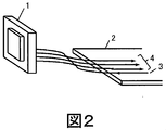
- FIG. 2 shows an example of signal line connection in such a CMOS camera.
- the camera element 1 and the image processing board 2 are connected by a serial communication line 3 and an image transmission line 4.
- the image transmission line 4 is a plurality of parallel signal lines.
- the serial communication line 3 is used for setting and checking the operation state of the camera.
- the image transmission line 4 is used to output an image detected by the camera element from the camera element.
- the number of signal lines of the camera element 1 increases, the package becomes larger due to the increase in the number of pins, and the cost increases.
- the number of wires (number of pins) is reduced.
- the number of image transmission lines 4 has increased particularly recently and has reached several tens.
- the data read from the camera element is required to have a high resolution and 10 megabytes. Furthermore, there is a demand for high-speed imaging at a rate of more than 200 frames per second so that shooting data per second reaches 1 to 3 gigabytes.
- CMOS cameras having the same number of AD converters as the number of horizontal pixels in the imaging area are appearing, and the present invention handles such high-speed camera elements. .
- a part of the camera element has a partial area transmission function in which only a required rectangular area is extracted from the captured image area, and image data of only that area can be transmitted and output. I have something to have. If this function can be used effectively, the frame rate of the camera element can be made higher than usual even when a package having the same number of pins is used by reducing the amount of data to be transmitted. By increasing the frame rate, the control can be speeded up in a control device such as an appearance inspection device.
- the data transmission speed of the camera element is limited by the package, and the data transmission time required to output the image data for one horizontal line to the outside of the camera element is substantially the same as the AD conversion time.
- More and more camera elements are being designed. In such a camera element, if the width of the partial transmission area is wide, the amount of image data to be transferred increases, so the waiting time until AD conversion ends first and data output to the outside of the camera element is lost. It becomes. On the other hand, when the horizontal width of the partial transmission area is small, the amount of image data is reduced, so that data output to the outside of the camera element ends first, and the waiting time until the end of AD conversion is lost.
- the image of the semicircular imaging region 11 is efficiently acquired as an example within the entire imageable range 10, as shown in FIG.
- the image data of each area can be read continuously, it is possible to transmit unnecessary portions above the arc as compared with the case of simply reading by partial transmission in one rectangular area.
- the efficiency of image acquisition can be improved.
- the rectangular area 12 has a wide width and a narrow width as described above, the waiting for the data output time may be lost and the waiting for the AD conversion end time may be lost as described above. A mixed case occurs. In this case, if these losses can be improved, the operation of the camera element can be further increased in frame rate.
- the imaging device, the control device, and the information reproducing device according to the present invention are devised so that the above-described loss can be eliminated and the operation speed can be increased when camera elements having a partial area transmission function are used in these devices.
- the camera element can be used at a higher frame rate while maintaining the cost.
- This camera element improves the efficiency of partial area transmission by two mechanisms.
- FIG. 1A in the case of an image having a semicircular imaging area 11 as an example within the entire imageable range 10, an area to be transmitted is first divided into a plurality of rectangles as shown in FIG. Are divided into rectangular regions 12. Then, corresponding to the pattern of FIG. 1B, two tables (table A and table A ′) for storing the upper left coordinates and lower right coordinates of each rectangle are prepared as shown in FIG. When obtaining an image of the imaging region 11, as shown in FIG.
- the partial region has a rectangular region having a wide width portion (wide portion) and a narrow width portion (narrow portion) depending on the location, the wide portion image data and the narrow portion image data.
- the maximum transmission data volume of the image data output by the camera can be reduced by reducing the average transmission data volume to an intermediate value between them. Even so, the frame rate can be improved. Even with the same number of package pins, an image can be transmitted at a higher frame rate. Thereby, the control of the control device and the operation of the information reproducing device can be speeded up.
- FIG. 3 shows the case of an image having a semicircular imaging area, as in FIG. 1A.
- the whole image is taken at a specific timing. In other cases, it may be sufficient to detect only the balance of the amount of light in the vertical and horizontal directions.
- the image data of the entire part of the imaging area 11 (FIG. 3 (a1)) is not always required, and usually the image data of the partial area as shown in FIG. 3 (b1) is continuously checked.
- the time required to transmit an image is proportional to the amount of area of image data to be transmitted.
- the entire portion of image data is acquired only when necessary.
- the frame rate can be significantly increased in the state of FIG. 3B1.
- the operation state is set by the serial communication line, and if these operation settings are rewritten by the serial communication line, the actual frame rate may decrease by 10 to 30%. Therefore, in this configuration, as shown in FIGS.
- a coordinate table corresponding to each of the A mode and the B mode is provided inside the camera element, and coordinate values representing the area shape of each mode are set in advance. It is stored in a table, and instantaneous switching is realized only by giving a signal for switching this mode from the outside.
- FIG. 4 shows the overall configuration of the circuit inside the camera element. This is the internal circuit configuration of the camera element 1 shown in FIG.
- the camera element communicates with a controller 21 that controls the whole of the camera element through a control input / output terminal 20 that is an input / output interface with an image processing board that is a higher-order system, or a table A22, a table B23, and a table A.
- a controller 21 that controls the whole of the camera element through a control input / output terminal 20 that is an input / output interface with an image processing board that is a higher-order system, or a table A22, a table B23, and a table A.
- Each coordinate value of '24, table B '25 can be set and the set value can be confirmed.
- Table A has the functions of Table A in FIG. 1C and FIG. 3A2
- table A ′ has the functions of Table A ′ in FIG. 1C and FIG. 3A2.
- the table B has the functions of the table A in FIG. 1 (c) and the function of FIG. 3 (b2)
- the table B ′ has the functions of the table A ′ in FIG.
- the controller 21 starts an image acquisition operation in response to a signal from the control input / output terminal 20.
- the controller 21 sends pulses to the pixel transfer signal 26 and the pixel reset signal 27 to reset the pixels before exposure.
- the pixel transfer signal 26 and the pixel reset signal 27 are connected to each pixel unit 29 in the pixel array region 28.
- a specific circuit example inside each pixel unit 29 is shown in FIG. Inside the pixel unit, the transistor is driven by a pixel transfer signal 26, a pixel reset signal 27, and a vertical drive signal 28 to control the movement of photodetection charges in each pixel.
- the controller 21 starts an image acquisition operation in response to a signal from the control input / output terminal 20.
- the controller 21 sends pulses to the pixel transfer signal 26 and the pixel reset signal 27 to reset the pixels before exposure.
- the pixel transfer signal 26 and the pixel reset signal 27 are connected to each pixel unit 29 in the pixel array region 28.
- a specific circuit example inside each pixel unit 29 is shown in FIG.
- the pixel transfer signal 26 when only the pixel transfer signal 26 is turned on, the charge proportional to the amount of light received by each pixel moves to the gate of the output transistor 30 of the pixel unit.
- the vertical drive signal 28 is turned on in this state, a voltage proportional to the amount of light received by each pixel is output from each pixel unit.
- the pixel reset signal can be driven separately for each row, and at the time of reading, the difference between the output voltage and the voltage immediately after the reset is taken to obtain a more accurate received light amount signal. Is omitted in the following description.
- the mode switching signal 31 for switching between the A mode and the B mode is determined in advance by this state.
- the values of the table A22 and the table A′24 are selected by the table selector 32 in the A mode, and the table B23 in the B mode.
- the value of the table B′25 are selected by the table selector 32 and latched in the table buffer 34 by the table latch signal 33 and stored. Note that these values can be instantaneously changed by simply sending a pulse to the table latch signal 33 after switching the mode switching signal 31 when switching between the A mode and the B mode.
- the controller 21 outputs a pulse to the initialization signal 35 to initialize each part of the circuit.
- the area counter 36 is reset.
- the XY coordinates (xs1 ′, ys1 ′) and the lower right XY coordinates (xe1 ′, ye1 ′) are selected by the coordinate selector 37 according to the value of the area counter 36, and the X coordinate range signal 38 (xs1 and xe1) and Y
- the coordinate range signal 39 (ys1 and ye1), the X ′ coordinate range signal 40 (xs1 ′ and xe1 ′), and the Y ′ coordinate range signal 41 (ys1 ′ and ye1 ′) are output.
- the Y coordinate range signal 39 is loaded to the vertical counter 42a by the initialization signal 35, and the initial value of the vertical counter 42a is ys1.
- the Y 'coordinate range signal 41 is input to the vertical counter 42b and loaded by the initialization signal 35, so that the initial value of the vertical counter 42b is ys1'.
- These values are selected by the Y coordinate selector 44 based on the output value of the flip-flop 43 and output as the Y coordinate value 45.
- the flip-flop 43 receives an AD conversion end signal 46 described later, and the Y coordinate count value and the Y ′ coordinate count value are alternately output as the Y coordinate value 45 for each AD conversion. Become.
- the Y coordinate value 45 is supplied to the vertical decoder 47, and the selection drive line 48 at the corresponding Y coordinate position in the pixel array region 28 is driven, and the pixels arranged in a horizontal row driven by the selection drive line 48.
- a voltage proportional to the detected light amount is output from the unit 29.
- These output voltages are input to the AD converter 51 through the vertical signal lines 50, and are AD converted using the AD conversion start signal 52 as a trigger.
- the AD conversion start signal 52 is generated by delaying the AD conversion start permission signal 54 output from the AND gate 53 by the time delay circuit 55.
- the output of the flip-flop 56 is supplied to the AND gate 53 via the OR gate 57, so that the AD conversion start permission signal 54 is turned on, and all the counters are turned on. Even when the operation is stopped, the AD converter 51 can start the AD conversion operation after the delay time by the time delay circuit 55 has elapsed. Further, when the AD conversion start permission signal 54 is turned on, the initial value is loaded to the horizontal counter described later.
- the AD conversion start permission signal 54 is supplied as a latch input of the line buffer 58.
- the line buffer 58 stores and holds the AD conversion value in the line buffer 58 and continues to supply the held AD conversion value to the horizontal selector 59 at the rising timing of the latch input after the AD conversion ends.
- the X coordinate range signal 38 and the X ′ coordinate range signal 40 are selected by the X coordinate selector 61 based on the value of the flip-flop 60, held in the X coordinate range value buffer 62, and output as the X coordinate range value signal 63.
- the flip-flop 60 receives an AD conversion end signal, which will be described later, and inverts the signal every time AD conversion starts.
- the X coordinate range value signal 63 becomes the value of the X coordinate range signal 38 (xs1 and xe1) immediately after initialization, and thereafter, every time AD conversion is resumed, the X coordinate range value (xs1 and xe1).
- X ′ coordinate range values (xs1 ′ and xe1 ′) are alternately output.
- the X coordinate range value buffer 62 is a rising edge trigger input.
- the X coordinate range value signal 63 is supplied to the horizontal counter 64 and determines the count range of the horizontal counter.
- the horizontal counter includes inputs of an X coordinate initial value load signal 65, an operation inhibition signal 66, and a horizontal scanning clock signal 67.
- the X-coordinate initial value load signal 65 is a rising trigger input. Further, since the output of the flip-flop 56 is supplied via the OR gate 57 and is turned on in the initial state, the operation prohibiting signal 66 input is locked in the initial state. Has been. This lock is released by the first AD conversion end signal.
- the X-coordinate initial value load signal 65 is generated by delaying the AD conversion start permission signal 54 by the gate. As described above, when the AD conversion start permission signal 54 is turned on, the horizontal counter 64 is turned on. Is already loaded with the initial initial value.
- the horizontal scanning clock signal 67 is always supplied from the horizontal scanning clock oscillation circuit 68, the horizontal counter starts counting as soon as the operation inhibition signal 66 is released.
- the horizontal counter starts the initial counting operation by the first AD conversion end signal, and at the same time, the AD conversion end signal 46 sends a clock to the vertical counter 42a that counts the Y coordinate value via the flip-flop 43.
- the vertical counter is counted up, and the Y coordinate count value of the vertical counter 42b is selected by the Y coordinate selector 44 and output as the Y coordinate value 45.
- the AD conversion start permission signal 54 is turned on, the AD conversion start signal 52 is supplied via the time delay circuit 55, and the AD converter 51 automatically starts the second conversion.
- the horizontal counter that has started the counting operation counts the X coordinate value in synchronization with the clock within the range given to the X coordinate range value signal 63, and outputs the counted X coordinate value and the clock.
- the horizontal selector 59 receives the counted X coordinate value and the clock, selects an AD conversion value at the horizontal coordinate position corresponding to the count value from the AD conversion values supplied from the line buffer 58, and the FIFO buffer 70. Output to (first-in first-out buffer).
- the FIFO buffer 70 outputs the AD conversion value received from the horizontal selector 59 in parallel from the differential transmission output 73 in synchronization with the transmission clock 72 generated by the differential transmission clock oscillator 71.
- the FIFO buffer 70 turns off the data valid signal 74 to indicate that the data is empty when there is no more data in the buffer.
- the data valid signal 74 and the transmission clock 72 are output from the differential transmission output 73 together.
- the FIFO buffer 70 outputs a buffer full signal 75 indicating that the data stored in the buffer has reached the upper limit that can be stored and becomes full.
- the buffer full signal 75 is input to the horizontal counter operation inhibition signal 66 through a gate, and during the period when the buffer is full, the count operation is temporarily stopped and waits until the FIFO buffer 70 becomes empty.
- the horizontal counter 64 When the AD conversion values of all horizontal lines in the X coordinate range are transferred to the FIFO buffer and the count value of the horizontal counter 64 exceeds the X coordinate range, the horizontal counter 64 outputs an X count full signal 76 and counts. By stopping the operation and notifying the AND gate 53 via the OR gate 57 that the horizontal counter is stopped, the AND gate 53 can turn on the AD conversion start permission signal 54 again and start the next AD conversion. Like.
- the flip-flop 43 is inverted again. This time, the vertical counter 42b is counted up via the flip-flop 43, and at the same time, the Y-coordinate selector 44 The Y coordinate count value of the vertical counter 42 a is output as the Y coordinate value 45.
- the X coordinate initial value load signal 65 is turned on, and the horizontal coordinate 64 is loaded with the X coordinate initial value again.
- the count full signal 76 is canceled, and the horizontal counter 64 starts the second counting operation of the X coordinate value again.
- the AD converter 51 starts the next third AD conversion operation.
- the AD converter performs the third AD conversion operation first.
- the AD converter operates to perform the next (N + 1) th AD conversion.
- the Y coordinate count value of the vertical counter 42b exceeds the Y coordinate range value.
- the Y counter full signal 80 is output from the vertical counter 42b.
- the Y count full signal 80 is input to the area counter 36 as a clock pulse, and the area counter 36 is counted up, whereby a new coordinate range (X coordinate range, Y coordinate range, X ′ coordinate range, Y ′ coordinate range) is output.
- a new Y coordinate range value is set in the vertical counter 42a
- a new Y ′ coordinate range value is set in the vertical counter 42b.
- the values of the X coordinate range and the X ′ coordinate range supplied to the X coordinate range value buffer 62 are also updated, and the output value of the X coordinate range value buffer 62 after the next AD conversion is completed is changed to the new X coordinate range.
- the value is updated to the value of the X ′ coordinate range and supplied to the horizontal counter 64.
- the procedure so far after initialization is repeated by the number of rectangular regions stored in the table, and finally the coordinate value of Y ′ (lower right coordinate) is a value representing the end.
- the comparator 81 detects that the value is set to 0, the output of the flip-flop 82 is inverted when the next horizontal counter count is full (at the end of FIFO transmission), and the operations of the horizontal counter 64 and the AD converter 51 are reversed. Is locked.
- a plurality of pairs of rectangular areas can be transmitted continuously and alternately. Since multiple pairs of areas can be specified, compared to the case where only one rectangular area can be specified, when obtaining an image of a semicircular or nearly elliptical partial area, the upper half of the semicircular area is divided more finely. Since unnecessary areas can be omitted, transmission efficiency can be increased and the frame rate can be increased.
- the AD converter operates to perform the next (N + 1) th AD conversion.
- the double buffer configuration of the line buffer 58 and the FIFO buffer 70 is employed, when the rectangular area of the wide part and the narrow part is alternately scanned for each horizontal line, image data of two horizontal line scans is obtained. Variations in the transmission amount can be absorbed by the double buffer configuration.
- the rectangular area coordinate values of the table A and the table A ′ even when the case where the waiting for the data output time is lost and the case where the waiting for the AD conversion end time is lost occur together.
- fluctuations in the data transmission amount can be absorbed by the double buffer configuration, and the average transmission data amount can be widened. It can be an intermediate value between the values in the region and the narrow region. That is, even when the data output time waiting becomes a loss and the case where the AD conversion end time waiting becomes a loss, these losses can be offset, and the frame rate of the camera element is Higher values can be used.
- switching of the shape of the partial area as shown in FIG. 3 (a1) or FIG. 3 (b1) can be realized without the need to rewrite the coordinate values of the table using serial communication.
- the shape of the partial area (A mode and B mode) can be switched without applying a loss, the loss of serial communication time associated with the switching operation can be omitted, and the frame rate can be improved.
- the operation at that time is the same as that in the configuration example of FIG. 4 described so far, except for the switching operation between the A mode and the B mode.
- the process of alternately switching between the table A and the table A ′ and the table B and the table B ′ becomes unnecessary.
- the table A′24, the table B′25, the table selector 32, the flip-flop 43, the vertical counter 42a, the Y coordinate selector 44, the flip-flop 60, and the X coordinate selector 61 may be omitted.
- the wiring for selecting X or X ′, Y or Y ′ the wiring that has disappeared due to the above omission is omitted, and the input of the remaining X or X ′, Y or Y ′, either wiring is omitted. Connect to the output after. In this case, the circuit can be simplified considerably.
- the connection between / Q, and Cp when the flip-flop 43 is omitted, the connection between / Q and Cp may be performed.
- the operation at that time is the same as that of the configuration example of FIG. 4 described so far, except for the switching operation of X or X ′, Y or Y ′.
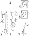
- FIG. 6A shows a configuration example of an imaging device using the camera element and a control device based on the taken image.
- the imaging object 101 placed on the moving belt 100 moves in the horizontal direction by the belt.
- a camera 102 in which the camera element 1 is stored is arranged so that the imaging object 101 can be photographed.
- Image data 116 output from the camera is supplied to the image analysis apparatus 103, and the position of the imaging target 101 is estimated based on the image, and the captured image of the imaging target 101 is recorded. Specifically, these constitute a product overview inspection device.
- FIG. 6 (b) shows connection with the control system around the apparatus shown in FIG. 6 (a).
- Information on the position estimated by the image analysis apparatus 103 is output to the timing predictor 104.
- the timing predictor 104 determines the timing at which the imaging target 101 reaches the specific position 105 based on the periodic position information 107 of the image analysis apparatus 103 with respect to the time 106 by linear interpolation (linear interpolation).
- the prediction arrival timing 108 is output to the image analysis apparatus 103. Note that the vertical axis in FIG.
- the image analysis apparatus 103 Based on the predicted arrival timing 108, the image analysis apparatus 103 sends an A / B mode switching signal 110, an exposure timing signal 111, and an area shape signal 112 having coordinate value information stored in advance in a plurality of coordinate value tables to the camera 102. Output. Inside the camera 102, these signals are supplied to the camera element 1 inside the camera. In the camera element 1, the B mode is used for shooting necessary for generating the periodic position information 107, and the A mode is used for shooting in a state where the image is correctly reflected in the center as shown in FIG. 6 (d2). The camera element 1 selects the shape of the partial area to be imaged according to the A / B mode switching signal 110 and captures an image of the imaging target 101 according to the exposure timing signal 111.
- the image recorded by the image analysis apparatus 103 does not shift as a whole as shown in FIG. 6 (d1), and the imaging target 101 is correctly centered in the imaging range 113 as shown in FIG. 6 (d2). Photographed in the reflected state. Further, the recorded image information is output from the image analysis device 103, and based on the image information, the sorting control device 114 determines the destination, and the driving device 115 classifies the destination to a suitable destination.
- the partial area transmission can be effectively switched and the frame rate can be increased.
- the timing prediction shown in FIG. 4 more accurate prediction is possible, and the position accuracy of the imaging object 101 to be finally photographed can be increased, and more accurate imaging makes the image processing simple and fast.
- the operation of the entire control device can be speeded up.
- an apparatus having a sorting function is given as an example of the control apparatus.
- the camera element 1 can be applied to a control apparatus in the information reproducing apparatus as described in the next section.
- FIG. 7A shows a configuration of an information reproducing device of a holographic memory as an example of an imaging device using the camera element and a control device based on a photographed image.
- the laser light 201 output from the laser light source 200 is split by the beam splitter 202 into reference light 203 and signal light 204 that go to the right side of the figure.
- the signal light 204 is reflected by the reflecting mirror 205, passes through the shutter 206, the beam expander 207, the phase mask 208, and the relay lens set 209, and is irradiated to the light modulator 211 by the polarization beam splitter 210.
- the optical modulator 211 is a combination of a polarizing plate and a liquid crystal substance, and modulates the phase of light two-dimensionally with liquid crystal.
- the light reflected by the light modulator 211 passes through the polarization beam splitter 210 and the relay lens 212 and is irradiated onto the disk 214 by the objective lens 213.
- the disk 214 is mounted on a spindle motor 215 and can be rotated to change the irradiation position on the disk.
- the reference light 203 is sequentially reflected by the reflecting mirror 220, the first galvanometer 221, and the second galvanometer 222, and is irradiated onto the disk 214 so as to cross the irradiation position of the signal light.
- the light is reflected by the three galvanometer 223 and returned to the disk 214 at substantially the same angle as the forward path.
- Each galvanometer is a movable mirror configured so that the angle can be accurately controlled by the controller 224.
- the mirror angle of the galvanometer is referred to as a galvanometer mirror angle.
- the light returned to the disk 214 is diffracted by the hologram written on the disk, and reversely follows the optical path through which the signal light has passed, passes through the objective lens 213 and the relay lens 212, and is polarized by the polarization beam splitter 210. The light is reflected rightward in the figure and is incident on the camera element 1.
- the camera element 1 the camera element described with reference to FIGS. 1 and 3 to 5 is used. Image data output from the camera element 1 is input to the controller 224 and is subjected to signal processing in the controller, thereby being restored as digital data.
- the shutter 206 is opened when data is recorded on the disk, and the shutter 206 is closed when data is reproduced from the disk, and the presence or absence of signal light is switched.
- the light read from the hologram recorded on the disk 214 at a constant reference light angle period and incident on the camera element 1 has a reproduced light intensity 230, which is the intensity, of the galvanometer mirror angle.
- the intensity changes in a wave shape with respect to 231.
- the angle of the reference light related to the reproduction light depends on all the angles of the first galvanometer 221, the second galvanometer 222, and the third galvanometer 223 in this configuration.
- the galvanometer mirror angle described here may be considered as one of those typical galvanometers.
- the galvano mirror angle 231 moves between peaks to a position where the reproduction signal intensity changing in a wave shape becomes a peak (maximum), and stops on the peak. It is usually used in intermittent drive operation (stop and go operation by repeated movement and stop). This is shown in FIG. This shows an operation of repeatedly moving and stopping the galvanometer mirror angle 231 to an angle at which the reproduction light intensity 230 reaches a peak.
- the galvanometer mirror angle 231 is plotted with respect to the time 232, the locus of the galvanometer mirror angle becomes like a terraced field.
- the imaging timing of the camera element is allowed to have some error in time, and although there is an advantage that mechanical control of the mirror angle is easy at the imaging timing 233, the operation of repeating the movement and stop mechanically is performed. For this reason, there is an upper limit on the operation speed due to the mechanical drive frequency limit of the galvanometer, and thus there is a problem that the information reproduction speed cannot be increased as the information reproduction apparatus.
- the mirror angle is not mechanically moved and stopped repeatedly, but as shown in FIG. 8B. If the image of the reproduction light can be detected at the maximum position of each peak by adjusting the shooting timing of the camera element 1 while the mirror angle continues to rotate at a constant speed, the information can be obtained without being bound by the mechanical drive frequency limit of the galvanometer. Can increase the playback speed.
- the A mode is used to detect the reproduction light image at the maximum position of each peak as shown in FIG. 8B, and the maximum position of each peak is predicted.
- the B mode is used to detect a partial image so that the feedback is accelerated.
- the timing predictor 234 is provided inside the controller 224, and the image detected by the camera element 1 is usually partially detected in the B mode. Between the controller 224 and the camera element 1, an A / B mode switching signal 235, an exposure timing signal 236, and an area shape signal 237 are provided.
- the timing predictor 234 assumes that the galvanometer mirror angle changes in proportion to the time 232, and uses the same curve as the previous peak from the periodic intensity information 238 that is information of the reproduction light intensity 230. As a result, the maximum intensity timing 239 at which the reproduction light intensity is maximum is estimated from the curve curve and output.
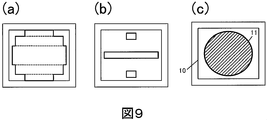
- the controller 224 switches the A / B mode switching signal 235 and drives the exposure timing signal 236 at the time coincident with the maximum intensity timing 239. To do. It should be noted that the pattern of FIG. 9A as the area shape corresponding to the A mode, the pattern of FIG.
- 9B as the area shape corresponding to the B mode, and the coordinate value table to the camera element 1 in advance by the area shape signal 237.
- 9A and 9B assumes a circular image as shown in FIG. 9C as an image of the hologram reproduction light detected by the camera element 1.
- the partial area transmission pattern is instantaneously switched, and until just before, the B mode partial transmission area is set.
- the frame rate can be increased, so that more accurate prediction is possible in the timing prediction shown in FIG. 9C, and the image of the hologram reproduction light that is finally photographed has the maximum intensity. Therefore, the hologram can be reproduced in a continuous rotation operation that continuously rotates at a constant speed instead of the conventional galvanometer mirror angle control by the intermittent drive operation. Thereby, the reproduction speed of information can be increased without being bound by the mechanical drive frequency limit of the galvanometer.
- this embodiment can be expressed as follows. That is, in an optical information reproducing apparatus that reproduces information from an optical information recording medium using holography, a laser light source that generates reference light and an angle adjuster that adjusts an incident angle of the reference light to the optical information recording medium And an image sensor that detects diffracted light reproduced from the optical information recording medium, the image sensor has a partial transmission function, and stores a pair of coordinate ranges of two rectangular areas; A line buffer of one horizontal line or more, having a function of acquiring imaging data from the two rectangular areas and transmitting the data alternately for each horizontal line, and an output from the imaging device is sent to the angle adjuster.
- An optical information reproducing apparatus characterized by being inputted.
- this invention is not limited to the above-mentioned Example, Various modifications are included.
- the above-described embodiments have been described in detail for easy understanding of the present invention, and are not necessarily limited to those having all the configurations described.
- a part of the configuration of one embodiment can be replaced with the configuration of another embodiment, and the configuration of another embodiment can be added to the configuration of one embodiment.
- each of the above-described configurations may be configured such that a part or all of the configuration is configured by hardware, or is realized by executing a program by a processor.
- control lines and information lines indicate what is considered necessary for the explanation, and not all the control lines and information lines on the product are necessarily shown. Actually, it may be considered that almost all the components are connected to each other.
Landscapes
- Physics & Mathematics (AREA)
- General Physics & Mathematics (AREA)
- Engineering & Computer Science (AREA)
- Multimedia (AREA)
- Signal Processing (AREA)
- Optics & Photonics (AREA)
- Studio Devices (AREA)
- Optical Recording Or Reproduction (AREA)
- Transforming Light Signals Into Electric Signals (AREA)
Abstract
Description
2 画像処理基板
3 シリアル通信線
4 画像伝送線
10 撮像可能範囲
11 撮像領域
12 矩形領域
20 制御入出力端子
21 制御器
22 テーブルA
23 テーブルB
24 テーブルA’
25 テーブルB’
26 画素転送信号
27 画素リセット信号
28 画素アレイ領域
29 画素ユニット
30 出力トランジスタ
31 モード切替信号
32 テーブルセレクタ
33 テーブルラッチ信号
34 テーブルバッファ
35 初期化信号
36 領域カウンタ
37 座標セレクタ
38 X座標範囲信号
39 Y座標範囲信号
40 X’座標範囲信号
41 Y’座標範囲信号
42a、42b 垂直カウンタ
43 フリップフロップ
44 Y座標セレクタ
45 Y座標値
46 AD変換終了信号
47 垂直デコーダ
48 選択駆動線
50 垂直信号線
51 AD変換器
52 AD変換開始信号
53 ANDゲート
54 AD変換開始許可信号
55 時間遅延回路
56 フリップフロップ
57 ORゲート
58 ラインバッファ
59 水平セレクタ
60 フリップフロップ
61 X座標セレクタ
62 X座標範囲値バッファ
63 X座標範囲値信号
64 水平カウンタ
65 X座標初期値ロード信号
66 動作禁止信号
67 水平走査クロック信号
68 水平走査クロック発振回路
70 FIFOバッファ
71 差動伝送クロック発振器
72 伝送クロック
73 差動伝送出力
74 データ有効信号
75 バッファフル信号
76 Xカウントフル信号
80 Yカウントフル信号
81 比較器
82 フリップフロップ
100 移動ベルト
101 撮像対象
102 カメラ
103 画像解析装置
104 タイミング予測器
105 特定位置
106 時間
107 定期的位置情報
108 予測到達タイミング
109 位置
110 A/Bモード切替信号
111 露光タイミング信号
112 領域形状信号
113 撮像範囲
114 仕分け制御装置
115 駆動装置
116 画像データ
200 レーザ光源
201 レーザ光
202 ビームスプリッタ
203 参照光
204 信号光
305 反射鏡
206 シャッタ
207 ビームエキスパンダ
208 位相マスク
209 リレーレンズ組
210 偏光ビームスプリッタ
211 光変調器
212 リレーレンズ
213 対物レンズ
214 ディスク
215 スピンドルモータ
220 反射鏡
221 第一ガルバノメータ
222 第二ガルバノメータ
223 第三ガルバノメータ
224 制御器
230 再生光強度
231 ガルバノミラー角度
232 時間
233 撮像タイミング
234 タイミング予測器
235 A/Bモード切替信号
236 露光タイミング信号
237 定期的強度情報
238 最大強度タイミング
Claims (11)
- ホログラフィを利用して光情報記録媒体から情報を再生する光情報再生装置において、
参照光を生成するレーザ光源と、
前記参照光の前記光情報記録媒体への入射角度を調節する角度調節器と、
前記光情報記録媒体から再生する回折光を検出する撮像素子とを備え、
前記撮像素子は部分伝送機能を有しており、2つの矩形領域の座標範囲をペアにして記憶するテーブルと、一水平線以上のラインバッファとを備え、前記2つの矩形領域より撮像データを取得して、一水平線ごとに交互に送信する機能を有しており、
前記撮像素子からの出力が前記角度調節器に入力されることを特徴とする光情報再生装置。 - 部分伝送機能を有する画像センサ素子と、
2つの矩形領域の座標範囲をペアにして記憶するテーブルと、
一水平線以上のラインバッファとを素子内に有し、
前記2つの矩形領域より撮像データを取得して、一水平線ごとに交互に送信する機能を有することを特徴とする画像センサ素子。 - 請求項2に記載の画像センサ素子において、
複数ペアの矩形領域の連続伝送機能を有することを特徴とする画像センサ素子。 - 請求項2に記載の画像センサ素子において、
素子内部にて、画像データの伝達に、ラインバッファとFIFOバッファの2重バッファ構成を用いたことを特徴とする画像センサ素子。 - 請求項2に記載の画像センサ素子を用いた、
略楕円形または半円形の領域を撮像する撮像装置。 - 請求項2に記載の画像センサ素子を用いた、ホログラム情報再生装置。
- 部分伝送機能を有する画像センサ素子と、
複数の矩形領域の座標範囲を記憶するテーブルと、
一回の転送指令によりテーブルに記憶された複数の座標範囲を連続かつ順に転送する機能を有する画像センサ素子。 - 請求項7に記載の画像センサ素子において、
複数の矩形領域の座標範囲を記憶するテーブルをセンサ素子内部に複数有し、
前記複数のテーブルを選択する選択機能を持ち、
前記選択機能の設定値によって前記複数のテーブル瞬時に切替可能であることを特徴とする画像センサ素子。 - 請求項7に記載の画像センサ素子と、
部分的に取得された画像より次の露光タイミングの予測を行う予測器と、
複数の座標値テーブルより特定の座標値テーブルを選択する切替機能とを有し、
前記選択された座標値テーブルにより画像取得領域の形状を切替えて、前記予測器の予測タイミングに従って、露光を開始し、画像を撮像することを特徴とした撮像装置。 - 請求項9に記載の撮像装置を用いた、制御装置。
- 請求項7に記載の画像センサ素子を用いた、ホログラム情報再生装置。
Priority Applications (3)
| Application Number | Priority Date | Filing Date | Title |
|---|---|---|---|
| JP2014551779A JPWO2014091570A1 (ja) | 2012-12-12 | 2012-12-12 | 撮像装置、制御装置および情報再生装置 |
| PCT/JP2012/082125 WO2014091570A1 (ja) | 2012-12-12 | 2012-12-12 | 撮像装置、制御装置および情報再生装置 |
| US14/651,475 US20160116887A1 (en) | 2012-12-12 | 2012-12-12 | Imaging device, control device, and information reproduction device |
Applications Claiming Priority (1)
| Application Number | Priority Date | Filing Date | Title |
|---|---|---|---|
| PCT/JP2012/082125 WO2014091570A1 (ja) | 2012-12-12 | 2012-12-12 | 撮像装置、制御装置および情報再生装置 |
Publications (1)
| Publication Number | Publication Date |
|---|---|
| WO2014091570A1 true WO2014091570A1 (ja) | 2014-06-19 |
Family
ID=50933894
Family Applications (1)
| Application Number | Title | Priority Date | Filing Date |
|---|---|---|---|
| PCT/JP2012/082125 Ceased WO2014091570A1 (ja) | 2012-12-12 | 2012-12-12 | 撮像装置、制御装置および情報再生装置 |
Country Status (3)
| Country | Link |
|---|---|
| US (1) | US20160116887A1 (ja) |
| JP (1) | JPWO2014091570A1 (ja) |
| WO (1) | WO2014091570A1 (ja) |
Families Citing this family (1)
| Publication number | Priority date | Publication date | Assignee | Title |
|---|---|---|---|---|
| JP6818724B2 (ja) * | 2018-10-01 | 2021-01-20 | キヤノン株式会社 | 放射線撮像装置、その制御方法及び放射線撮像システム |
Citations (4)
| Publication number | Priority date | Publication date | Assignee | Title |
|---|---|---|---|---|
| JPH07141104A (ja) * | 1993-11-19 | 1995-06-02 | Sharp Corp | 座標入力装置、座標特定情報の表示装置および方法ならびに座標特定情報表示板 |
| JPH08171620A (ja) * | 1994-12-16 | 1996-07-02 | Olympus Optical Co Ltd | 情報記録媒体及び情報再生システム |
| JP2006228375A (ja) * | 2005-02-21 | 2006-08-31 | Alps Electric Co Ltd | ホログラフィー記録装置,再生装置及びその方法並びにホログラフィー媒体 |
| JP2007534016A (ja) * | 2004-04-16 | 2007-11-22 | ディーシーイー アプリリス インコーポレーテッド | ホログラフィックメディア較正機構を用いたホログラフィックデータストレージシステムの較正 |
Family Cites Families (1)
| Publication number | Priority date | Publication date | Assignee | Title |
|---|---|---|---|---|
| JP5079736B2 (ja) * | 2009-04-20 | 2012-11-21 | ソニー株式会社 | ホログラム再生および撮像装置、ホログラム再生および撮像方法 |
-
2012
- 2012-12-12 WO PCT/JP2012/082125 patent/WO2014091570A1/ja not_active Ceased
- 2012-12-12 JP JP2014551779A patent/JPWO2014091570A1/ja active Pending
- 2012-12-12 US US14/651,475 patent/US20160116887A1/en not_active Abandoned
Patent Citations (4)
| Publication number | Priority date | Publication date | Assignee | Title |
|---|---|---|---|---|
| JPH07141104A (ja) * | 1993-11-19 | 1995-06-02 | Sharp Corp | 座標入力装置、座標特定情報の表示装置および方法ならびに座標特定情報表示板 |
| JPH08171620A (ja) * | 1994-12-16 | 1996-07-02 | Olympus Optical Co Ltd | 情報記録媒体及び情報再生システム |
| JP2007534016A (ja) * | 2004-04-16 | 2007-11-22 | ディーシーイー アプリリス インコーポレーテッド | ホログラフィックメディア較正機構を用いたホログラフィックデータストレージシステムの較正 |
| JP2006228375A (ja) * | 2005-02-21 | 2006-08-31 | Alps Electric Co Ltd | ホログラフィー記録装置,再生装置及びその方法並びにホログラフィー媒体 |
Also Published As
| Publication number | Publication date |
|---|---|
| JPWO2014091570A1 (ja) | 2017-01-05 |
| US20160116887A1 (en) | 2016-04-28 |
Similar Documents
| Publication | Publication Date | Title |
|---|---|---|
| JP2017147720A (ja) | ズーム機構を備えた撮像装置及び交換レンズ | |
| Höfling et al. | ALP: universal DMD controller for metrology and testing | |
| US20070052837A1 (en) | Imaging apparatus with auto-focus function | |
| CN113945949A (zh) | 多功能飞行时间传感器及操作其的方法 | |
| JP2009065605A (ja) | 移動型撮像装置および撮像方法 | |
| JP2012023650A (ja) | 撮像装置 | |
| JP4439397B2 (ja) | 記録装置、再生装置及び記録再生装置 | |
| WO2014091570A1 (ja) | 撮像装置、制御装置および情報再生装置 | |
| CN101399902A (zh) | 固态成像装置和成像设备 | |
| CN101321229A (zh) | 摄像设备及其控制方法 | |
| CN104854657B (zh) | 光信息记录再现装置、光信息记录再现方法 | |
| TW201018961A (en) | Method and device for projecting at least one beam | |
| JP2014209721A (ja) | 撮像装置 | |
| US5706051A (en) | Compact optical system for electronic camera | |
| JP4455709B2 (ja) | 固体撮像装置および撮像方法 | |
| JP3744301B2 (ja) | 画像読み取り装置 | |
| US10321041B2 (en) | Imaging apparatus, control method of imaging apparatus, and non-transitory storage medium storing control method of imaging apparatus | |
| JP2003333429A (ja) | 撮像素子の駆動制御方法,撮像装置及び撮像システム | |
| US6334002B2 (en) | Image reader apparatus | |
| JP2020030521A (ja) | 画像処理装置 | |
| US20130155301A1 (en) | Image pickup apparatus, image pickup method, and machine-readable storage medium | |
| JP2007043707A (ja) | 自動焦点調節機能の付いたcmosイメージセンサ及びそれを含むカメラ装置 | |
| KR100739312B1 (ko) | 홀로그래픽 디지털 저장 시스템의 기록/재생 장치 및 방법 | |
| JPH02118505A (ja) | カメラのためのオートフォーカス装置 | |
| JP2006215066A (ja) | ホログラフィー記録装置,再生装置及びその方法並びにホログラフィー媒体 |
Legal Events
| Date | Code | Title | Description |
|---|---|---|---|
| 121 | Ep: the epo has been informed by wipo that ep was designated in this application |
Ref document number: 12890120 Country of ref document: EP Kind code of ref document: A1 |
|
| ENP | Entry into the national phase |
Ref document number: 2014551779 Country of ref document: JP Kind code of ref document: A |
|
| NENP | Non-entry into the national phase |
Ref country code: DE |
|
| WWE | Wipo information: entry into national phase |
Ref document number: 14651475 Country of ref document: US |
|
| 122 | Ep: pct application non-entry in european phase |
Ref document number: 12890120 Country of ref document: EP Kind code of ref document: A1 |