WO2014087913A1 - 有機エレクトロルミネッセンス素子 - Google Patents
有機エレクトロルミネッセンス素子 Download PDFInfo
- Publication number
- WO2014087913A1 WO2014087913A1 PCT/JP2013/082030 JP2013082030W WO2014087913A1 WO 2014087913 A1 WO2014087913 A1 WO 2014087913A1 JP 2013082030 W JP2013082030 W JP 2013082030W WO 2014087913 A1 WO2014087913 A1 WO 2014087913A1
- Authority
- WO
- WIPO (PCT)
- Prior art keywords
- light emitting
- host material
- emitting layer
- group
- layer
- Prior art date
Links
- 239000000463 material Substances 0.000 claims abstract description 223
- 239000002019 doping agent Substances 0.000 claims abstract description 41
- 238000005401 electroluminescence Methods 0.000 claims description 11
- JUJWROOIHBZHMG-UHFFFAOYSA-N Pyridine Chemical class C1=CC=NC=C1 JUJWROOIHBZHMG-UHFFFAOYSA-N 0.000 claims description 3
- 238000004020 luminiscence type Methods 0.000 claims 1
- 239000010410 layer Substances 0.000 description 325
- 150000001875 compounds Chemical class 0.000 description 75
- 125000004432 carbon atom Chemical group C* 0.000 description 53
- 230000032258 transport Effects 0.000 description 53
- 238000002347 injection Methods 0.000 description 46
- 239000007924 injection Substances 0.000 description 46
- 125000002029 aromatic hydrocarbon group Chemical group 0.000 description 36
- 230000005525 hole transport Effects 0.000 description 33
- 230000004888 barrier function Effects 0.000 description 22
- 125000001424 substituent group Chemical group 0.000 description 21
- -1 diamine compounds Chemical class 0.000 description 20
- 230000015572 biosynthetic process Effects 0.000 description 18
- 238000003786 synthesis reaction Methods 0.000 description 17
- 125000000217 alkyl group Chemical group 0.000 description 16
- 125000003118 aryl group Chemical group 0.000 description 16
- 238000005259 measurement Methods 0.000 description 16
- 125000006615 aromatic heterocyclic group Chemical group 0.000 description 15
- 125000000623 heterocyclic group Chemical group 0.000 description 15
- 125000000609 carbazolyl group Chemical group C1(=CC=CC=2C3=CC=CC=C3NC12)* 0.000 description 13
- 125000004429 atom Chemical group 0.000 description 12
- 238000000034 method Methods 0.000 description 12
- 150000002894 organic compounds Chemical class 0.000 description 12
- 239000000758 substrate Substances 0.000 description 12
- 238000000862 absorption spectrum Methods 0.000 description 10
- 125000004435 hydrogen atom Chemical group [H]* 0.000 description 10
- 125000004433 nitrogen atom Chemical group N* 0.000 description 10
- YXFVVABEGXRONW-UHFFFAOYSA-N Toluene Chemical compound CC1=CC=CC=C1 YXFVVABEGXRONW-UHFFFAOYSA-N 0.000 description 9
- 238000006243 chemical reaction Methods 0.000 description 9
- 230000000052 comparative effect Effects 0.000 description 9
- 125000006413 ring segment Chemical group 0.000 description 9
- QJGQUHMNIGDVPM-UHFFFAOYSA-N nitrogen group Chemical group [N] QJGQUHMNIGDVPM-UHFFFAOYSA-N 0.000 description 8
- BASFCYQUMIYNBI-UHFFFAOYSA-N platinum Chemical compound [Pt] BASFCYQUMIYNBI-UHFFFAOYSA-N 0.000 description 8
- 125000003545 alkoxy group Chemical group 0.000 description 7
- 150000001412 amines Chemical class 0.000 description 7
- 125000005843 halogen group Chemical group 0.000 description 7
- 229910052751 metal Inorganic materials 0.000 description 7
- 239000002184 metal Substances 0.000 description 7
- 239000000243 solution Substances 0.000 description 7
- XKRFYHLGVUSROY-UHFFFAOYSA-N Argon Chemical compound [Ar] XKRFYHLGVUSROY-UHFFFAOYSA-N 0.000 description 6
- ZMXDDKWLCZADIW-UHFFFAOYSA-N N,N-Dimethylformamide Chemical compound CN(C)C=O ZMXDDKWLCZADIW-UHFFFAOYSA-N 0.000 description 6
- KDLHZDBZIXYQEI-UHFFFAOYSA-N Palladium Chemical compound [Pd] KDLHZDBZIXYQEI-UHFFFAOYSA-N 0.000 description 6
- 150000004696 coordination complex Chemical class 0.000 description 6
- 125000004093 cyano group Chemical group *C#N 0.000 description 6
- 150000004891 diazines Chemical class 0.000 description 6
- 230000006798 recombination Effects 0.000 description 6
- 238000005215 recombination Methods 0.000 description 6
- 150000003918 triazines Chemical class 0.000 description 6
- 125000004104 aryloxy group Chemical group 0.000 description 5
- 229910052799 carbon Inorganic materials 0.000 description 5
- 238000003795 desorption Methods 0.000 description 5
- 230000005284 excitation Effects 0.000 description 5
- 239000011521 glass Substances 0.000 description 5
- 238000010438 heat treatment Methods 0.000 description 5
- 238000001819 mass spectrum Methods 0.000 description 5
- 239000000203 mixture Substances 0.000 description 5
- 239000012044 organic layer Substances 0.000 description 5
- 229910052705 radium Inorganic materials 0.000 description 5
- 229910052701 rubidium Inorganic materials 0.000 description 5
- 0 *C(*)(CC*1ccc2)c3c4c1c2ccc4ccc3 Chemical compound *C(*)(CC*1ccc2)c3c4c1c2ccc4ccc3 0.000 description 4
- 125000004070 6 membered heterocyclic group Chemical group 0.000 description 4
- XLOMVQKBTHCTTD-UHFFFAOYSA-N Zinc monoxide Chemical compound [Zn]=O XLOMVQKBTHCTTD-UHFFFAOYSA-N 0.000 description 4
- 125000003342 alkenyl group Chemical group 0.000 description 4
- 125000004453 alkoxycarbonyl group Chemical group 0.000 description 4
- 125000005103 alkyl silyl group Chemical group 0.000 description 4
- 238000004458 analytical method Methods 0.000 description 4
- MWPLVEDNUUSJAV-UHFFFAOYSA-N anthracene Chemical compound C1=CC=CC2=CC3=CC=CC=C3C=C21 MWPLVEDNUUSJAV-UHFFFAOYSA-N 0.000 description 4
- 125000003710 aryl alkyl group Chemical group 0.000 description 4
- 125000005104 aryl silyl group Chemical group 0.000 description 4
- 150000001721 carbon Chemical group 0.000 description 4
- 230000007423 decrease Effects 0.000 description 4
- 229910044991 metal oxide Inorganic materials 0.000 description 4
- 150000004706 metal oxides Chemical class 0.000 description 4
- YNPNZTXNASCQKK-UHFFFAOYSA-N phenanthrene Chemical group C1=CC=C2C3=CC=CC=C3C=CC2=C1 YNPNZTXNASCQKK-UHFFFAOYSA-N 0.000 description 4
- 125000001997 phenyl group Chemical group [H]C1=C([H])C([H])=C(*)C([H])=C1[H] 0.000 description 4
- 125000000843 phenylene group Chemical group C1(=C(C=CC=C1)*)* 0.000 description 4
- 239000007787 solid Substances 0.000 description 4
- 230000003595 spectral effect Effects 0.000 description 4
- 238000001228 spectrum Methods 0.000 description 4
- 239000000126 substance Substances 0.000 description 4
- 238000007740 vapor deposition Methods 0.000 description 4
- YFCSASDLEBELEU-UHFFFAOYSA-N 3,4,5,6,9,10-hexazatetracyclo[12.4.0.02,7.08,13]octadeca-1(18),2(7),3,5,8(13),9,11,14,16-nonaene-11,12,15,16,17,18-hexacarbonitrile Chemical group N#CC1=C(C#N)C(C#N)=C2C3=C(C#N)C(C#N)=NN=C3C3=NN=NN=C3C2=C1C#N YFCSASDLEBELEU-UHFFFAOYSA-N 0.000 description 3
- UHOVQNZJYSORNB-UHFFFAOYSA-N Benzene Chemical compound C1=CC=CC=C1 UHOVQNZJYSORNB-UHFFFAOYSA-N 0.000 description 3
- UJOBWOGCFQCDNV-UHFFFAOYSA-N Carbazole Natural products C1=CC=C2C3=CC=CC=C3NC2=C1 UJOBWOGCFQCDNV-UHFFFAOYSA-N 0.000 description 3
- RTZKZFJDLAIYFH-UHFFFAOYSA-N Diethyl ether Chemical compound CCOCC RTZKZFJDLAIYFH-UHFFFAOYSA-N 0.000 description 3
- YLQBMQCUIZJEEH-UHFFFAOYSA-N Furan Chemical compound C=1C=COC=1 YLQBMQCUIZJEEH-UHFFFAOYSA-N 0.000 description 3
- KFZMGEQAYNKOFK-UHFFFAOYSA-N Isopropanol Chemical compound CC(C)O KFZMGEQAYNKOFK-UHFFFAOYSA-N 0.000 description 3
- 238000002835 absorbance Methods 0.000 description 3
- 238000010521 absorption reaction Methods 0.000 description 3
- 229910052786 argon Inorganic materials 0.000 description 3
- 238000004364 calculation method Methods 0.000 description 3
- 125000003178 carboxy group Chemical group [H]OC(*)=O 0.000 description 3
- 230000008859 change Effects 0.000 description 3
- 238000001816 cooling Methods 0.000 description 3
- 125000000753 cycloalkyl group Chemical group 0.000 description 3
- TXCDCPKCNAJMEE-UHFFFAOYSA-N dibenzofuran Chemical compound C1=CC=C2C3=CC=CC=C3OC2=C1 TXCDCPKCNAJMEE-UHFFFAOYSA-N 0.000 description 3
- 230000005684 electric field Effects 0.000 description 3
- 238000011156 evaluation Methods 0.000 description 3
- 230000005283 ground state Effects 0.000 description 3
- 125000001188 haloalkyl group Chemical group 0.000 description 3
- 125000005842 heteroatom Chemical group 0.000 description 3
- 125000002887 hydroxy group Chemical group [H]O* 0.000 description 3
- RAXXELZNTBOGNW-UHFFFAOYSA-N imidazole Natural products C1=CNC=N1 RAXXELZNTBOGNW-UHFFFAOYSA-N 0.000 description 3
- 238000001566 impedance spectroscopy Methods 0.000 description 3
- 239000003446 ligand Substances 0.000 description 3
- 125000005647 linker group Chemical group 0.000 description 3
- 229910052749 magnesium Inorganic materials 0.000 description 3
- 239000011777 magnesium Substances 0.000 description 3
- 230000004048 modification Effects 0.000 description 3
- 238000012986 modification Methods 0.000 description 3
- 125000001624 naphthyl group Chemical group 0.000 description 3
- 125000000449 nitro group Chemical group [O-][N+](*)=O 0.000 description 3
- 238000001296 phosphorescence spectrum Methods 0.000 description 3
- 229910052697 platinum Inorganic materials 0.000 description 3
- 239000000843 powder Substances 0.000 description 3
- 239000010453 quartz Substances 0.000 description 3
- 230000004044 response Effects 0.000 description 3
- VYPSYNLAJGMNEJ-UHFFFAOYSA-N silicon dioxide Inorganic materials O=[Si]=O VYPSYNLAJGMNEJ-UHFFFAOYSA-N 0.000 description 3
- 238000002834 transmittance Methods 0.000 description 3
- 125000005580 triphenylene group Chemical group 0.000 description 3
- IANQTJSKSUMEQM-UHFFFAOYSA-N 1-benzofuran Chemical compound C1=CC=C2OC=CC2=C1 IANQTJSKSUMEQM-UHFFFAOYSA-N 0.000 description 2
- FCEHBMOGCRZNNI-UHFFFAOYSA-N 1-benzothiophene Chemical compound C1=CC=C2SC=CC2=C1 FCEHBMOGCRZNNI-UHFFFAOYSA-N 0.000 description 2
- IJGRMHOSHXDMSA-UHFFFAOYSA-N Atomic nitrogen Chemical compound N#N IJGRMHOSHXDMSA-UHFFFAOYSA-N 0.000 description 2
- KAKZBPTYRLMSJV-UHFFFAOYSA-N Butadiene Chemical compound C=CC=C KAKZBPTYRLMSJV-UHFFFAOYSA-N 0.000 description 2
- OKTJSMMVPCPJKN-UHFFFAOYSA-N Carbon Chemical group [C] OKTJSMMVPCPJKN-UHFFFAOYSA-N 0.000 description 2
- XTHFKEDIFFGKHM-UHFFFAOYSA-N Dimethoxyethane Chemical compound COCCOC XTHFKEDIFFGKHM-UHFFFAOYSA-N 0.000 description 2
- LFQSCWFLJHTTHZ-UHFFFAOYSA-N Ethanol Chemical compound CCO LFQSCWFLJHTTHZ-UHFFFAOYSA-N 0.000 description 2
- PCLIMKBDDGJMGD-UHFFFAOYSA-N N-bromosuccinimide Chemical compound BrN1C(=O)CCC1=O PCLIMKBDDGJMGD-UHFFFAOYSA-N 0.000 description 2
- UFWIBTONFRDIAS-UHFFFAOYSA-N Naphthalene Chemical compound C1=CC=CC2=CC=CC=C21 UFWIBTONFRDIAS-UHFFFAOYSA-N 0.000 description 2
- KYQCOXFCLRTKLS-UHFFFAOYSA-N Pyrazine Chemical compound C1=CN=CC=N1 KYQCOXFCLRTKLS-UHFFFAOYSA-N 0.000 description 2
- CDBYLPFSWZWCQE-UHFFFAOYSA-L Sodium Carbonate Chemical compound [Na+].[Na+].[O-]C([O-])=O CDBYLPFSWZWCQE-UHFFFAOYSA-L 0.000 description 2
- FAPWRFPIFSIZLT-UHFFFAOYSA-M Sodium chloride Chemical compound [Na+].[Cl-] FAPWRFPIFSIZLT-UHFFFAOYSA-M 0.000 description 2
- 235000002597 Solanum melongena Nutrition 0.000 description 2
- YTPLMLYBLZKORZ-UHFFFAOYSA-N Thiophene Chemical compound C=1C=CSC=1 YTPLMLYBLZKORZ-UHFFFAOYSA-N 0.000 description 2
- CUJRVFIICFDLGR-UHFFFAOYSA-N acetylacetonate Chemical compound CC(=O)[CH-]C(C)=O CUJRVFIICFDLGR-UHFFFAOYSA-N 0.000 description 2
- 229910052782 aluminium Inorganic materials 0.000 description 2
- 125000005110 aryl thio group Chemical group 0.000 description 2
- 229910052788 barium Inorganic materials 0.000 description 2
- DSAJWYNOEDNPEQ-UHFFFAOYSA-N barium atom Chemical compound [Ba] DSAJWYNOEDNPEQ-UHFFFAOYSA-N 0.000 description 2
- 150000001555 benzenes Chemical group 0.000 description 2
- JZOIZKBKSZMVRV-UHFFFAOYSA-N benzo(a)triphenylene Chemical group C1=CC=CC2=C3C4=CC=CC=C4C=CC3=C(C=CC=C3)C3=C21 JZOIZKBKSZMVRV-UHFFFAOYSA-N 0.000 description 2
- WZJYKHNJTSNBHV-UHFFFAOYSA-N benzo[h]quinoline Chemical group C1=CN=C2C3=CC=CC=C3C=CC2=C1 WZJYKHNJTSNBHV-UHFFFAOYSA-N 0.000 description 2
- 125000006267 biphenyl group Chemical group 0.000 description 2
- 239000005388 borosilicate glass Substances 0.000 description 2
- WDECIBYCCFPHNR-UHFFFAOYSA-N chrysene Chemical compound C1=CC=CC2=CC=C3C4=CC=CC=C4C=CC3=C21 WDECIBYCCFPHNR-UHFFFAOYSA-N 0.000 description 2
- 238000004140 cleaning Methods 0.000 description 2
- 238000000576 coating method Methods 0.000 description 2
- VPUGDVKSAQVFFS-UHFFFAOYSA-N coronene Chemical compound C1=C(C2=C34)C=CC3=CC=C(C=C3)C4=C4C3=CC=C(C=C3)C4=C2C3=C1 VPUGDVKSAQVFFS-UHFFFAOYSA-N 0.000 description 2
- ZSWFCLXCOIISFI-UHFFFAOYSA-N cyclopentadiene Chemical compound C1C=CC=C1 ZSWFCLXCOIISFI-UHFFFAOYSA-N 0.000 description 2
- 125000004663 dialkyl amino group Chemical group 0.000 description 2
- IYYZUPMFVPLQIF-UHFFFAOYSA-N dibenzothiophene Chemical compound C1=CC=C2C3=CC=CC=C3SC2=C1 IYYZUPMFVPLQIF-UHFFFAOYSA-N 0.000 description 2
- 230000005281 excited state Effects 0.000 description 2
- 150000002219 fluoranthenes Chemical group 0.000 description 2
- 229910052731 fluorine Inorganic materials 0.000 description 2
- 125000001153 fluoro group Chemical group F* 0.000 description 2
- 150000002430 hydrocarbons Chemical group 0.000 description 2
- 238000005286 illumination Methods 0.000 description 2
- PJULCNAVAGQLAT-UHFFFAOYSA-N indeno[2,1-a]fluorene Chemical class C1=CC=C2C=C3C4=CC5=CC=CC=C5C4=CC=C3C2=C1 PJULCNAVAGQLAT-UHFFFAOYSA-N 0.000 description 2
- 229910052741 iridium Inorganic materials 0.000 description 2
- GKOZUEZYRPOHIO-UHFFFAOYSA-N iridium atom Chemical compound [Ir] GKOZUEZYRPOHIO-UHFFFAOYSA-N 0.000 description 2
- QWTDNUCVQCZILF-UHFFFAOYSA-N isopentane Chemical compound CCC(C)C QWTDNUCVQCZILF-UHFFFAOYSA-N 0.000 description 2
- 125000005956 isoquinolyl group Chemical group 0.000 description 2
- 239000001989 lithium alloy Substances 0.000 description 2
- 238000004519 manufacturing process Methods 0.000 description 2
- 238000000691 measurement method Methods 0.000 description 2
- 150000002736 metal compounds Chemical class 0.000 description 2
- 239000003960 organic solvent Substances 0.000 description 2
- 125000004430 oxygen atom Chemical group O* 0.000 description 2
- 229910052763 palladium Inorganic materials 0.000 description 2
- NFHFRUOZVGFOOS-UHFFFAOYSA-N palladium;triphenylphosphane Chemical compound [Pd].C1=CC=CC=C1P(C=1C=CC=CC=1)C1=CC=CC=C1.C1=CC=CC=C1P(C=1C=CC=CC=1)C1=CC=CC=C1.C1=CC=CC=C1P(C=1C=CC=CC=1)C1=CC=CC=C1.C1=CC=CC=C1P(C=1C=CC=CC=1)C1=CC=CC=C1 NFHFRUOZVGFOOS-UHFFFAOYSA-N 0.000 description 2
- HXITXNWTGFUOAU-UHFFFAOYSA-N phenylboronic acid Chemical compound OB(O)C1=CC=CC=C1 HXITXNWTGFUOAU-UHFFFAOYSA-N 0.000 description 2
- 229920000642 polymer Polymers 0.000 description 2
- 238000005381 potential energy Methods 0.000 description 2
- BBEAQIROQSPTKN-UHFFFAOYSA-N pyrene Chemical compound C1=CC=C2C=CC3=CC=CC4=CC=C1C2=C43 BBEAQIROQSPTKN-UHFFFAOYSA-N 0.000 description 2
- 125000004076 pyridyl group Chemical group 0.000 description 2
- CYIDZMCFTVVTJO-UHFFFAOYSA-N pyromellitic acid Chemical compound OC(=O)C1=CC(C(O)=O)=C(C(O)=O)C=C1C(O)=O CYIDZMCFTVVTJO-UHFFFAOYSA-N 0.000 description 2
- 125000005493 quinolyl group Chemical group 0.000 description 2
- 239000002994 raw material Substances 0.000 description 2
- 238000010992 reflux Methods 0.000 description 2
- 230000000630 rising effect Effects 0.000 description 2
- 229920006395 saturated elastomer Polymers 0.000 description 2
- 238000010898 silica gel chromatography Methods 0.000 description 2
- 229910052709 silver Inorganic materials 0.000 description 2
- 125000003808 silyl group Chemical group [H][Si]([H])([H])[*] 0.000 description 2
- 238000009751 slip forming Methods 0.000 description 2
- 239000002904 solvent Substances 0.000 description 2
- 229910052717 sulfur Inorganic materials 0.000 description 2
- 125000004434 sulfur atom Chemical group 0.000 description 2
- PCCVSPMFGIFTHU-UHFFFAOYSA-N tetracyanoquinodimethane Chemical class N#CC(C#N)=C1C=CC(=C(C#N)C#N)C=C1 PCCVSPMFGIFTHU-UHFFFAOYSA-N 0.000 description 2
- 238000001771 vacuum deposition Methods 0.000 description 2
- XLYOFNOQVPJJNP-UHFFFAOYSA-N water Chemical compound O XLYOFNOQVPJJNP-UHFFFAOYSA-N 0.000 description 2
- 230000003313 weakening effect Effects 0.000 description 2
- 239000011787 zinc oxide Substances 0.000 description 2
- CYPYTURSJDMMMP-WVCUSYJESA-N (1e,4e)-1,5-diphenylpenta-1,4-dien-3-one;palladium Chemical compound [Pd].[Pd].C=1C=CC=CC=1\C=C\C(=O)\C=C\C1=CC=CC=C1.C=1C=CC=CC=1\C=C\C(=O)\C=C\C1=CC=CC=C1.C=1C=CC=CC=1\C=C\C(=O)\C=C\C1=CC=CC=C1 CYPYTURSJDMMMP-WVCUSYJESA-N 0.000 description 1
- UWRZIZXBOLBCON-VOTSOKGWSA-N (e)-2-phenylethenamine Chemical class N\C=C\C1=CC=CC=C1 UWRZIZXBOLBCON-VOTSOKGWSA-N 0.000 description 1
- POILWHVDKZOXJZ-ARJAWSKDSA-M (z)-4-oxopent-2-en-2-olate Chemical compound C\C([O-])=C\C(C)=O POILWHVDKZOXJZ-ARJAWSKDSA-M 0.000 description 1
- JYEUMXHLPRZUAT-UHFFFAOYSA-N 1,2,3-triazine Chemical group C1=CN=NN=C1 JYEUMXHLPRZUAT-UHFFFAOYSA-N 0.000 description 1
- YJTKZCDBKVTVBY-UHFFFAOYSA-N 1,3-Diphenylbenzene Chemical group C1=CC=CC=C1C1=CC=CC(C=2C=CC=CC=2)=C1 YJTKZCDBKVTVBY-UHFFFAOYSA-N 0.000 description 1
- 125000000355 1,3-benzoxazolyl group Chemical group O1C(=NC2=C1C=CC=C2)* 0.000 description 1
- UVHXEHGUEKARKZ-UHFFFAOYSA-N 1-ethenylanthracene Chemical compound C1=CC=C2C=C3C(C=C)=CC=CC3=CC2=C1 UVHXEHGUEKARKZ-UHFFFAOYSA-N 0.000 description 1
- GUPMCMZMDAGSPF-UHFFFAOYSA-N 1-phenylbuta-1,3-dienylbenzene Chemical compound C=1C=CC=CC=1[C](C=C[CH2])C1=CC=CC=C1 GUPMCMZMDAGSPF-UHFFFAOYSA-N 0.000 description 1
- NIDFGXDXQKPZMA-UHFFFAOYSA-N 14h-benz[4,5]isoquino[2,1-a]perimidin-14-one Chemical compound C1=CC(N2C(=O)C=3C4=C(C2=N2)C=CC=C4C=CC=3)=C3C2=CC=CC3=C1 NIDFGXDXQKPZMA-UHFFFAOYSA-N 0.000 description 1
- DPVIABCMTHHTGB-UHFFFAOYSA-N 2,4,6-trichloropyrimidine Chemical compound ClC1=CC(Cl)=NC(Cl)=N1 DPVIABCMTHHTGB-UHFFFAOYSA-N 0.000 description 1
- MGADZUXDNSDTHW-UHFFFAOYSA-N 2H-pyran Chemical compound C1OC=CC=C1 MGADZUXDNSDTHW-UHFFFAOYSA-N 0.000 description 1
- GOLORTLGFDVFDW-UHFFFAOYSA-N 3-(1h-benzimidazol-2-yl)-7-(diethylamino)chromen-2-one Chemical compound C1=CC=C2NC(C3=CC4=CC=C(C=C4OC3=O)N(CC)CC)=NC2=C1 GOLORTLGFDVFDW-UHFFFAOYSA-N 0.000 description 1
- CMSGUKVDXXTJDQ-UHFFFAOYSA-N 4-(2-naphthalen-1-ylethylamino)-4-oxobutanoic acid Chemical compound C1=CC=C2C(CCNC(=O)CCC(=O)O)=CC=CC2=C1 CMSGUKVDXXTJDQ-UHFFFAOYSA-N 0.000 description 1
- BPMBNLJJRKCCRT-UHFFFAOYSA-N 4-phenylbenzonitrile Chemical compound C1=CC(C#N)=CC=C1C1=CC=CC=C1 BPMBNLJJRKCCRT-UHFFFAOYSA-N 0.000 description 1
- ZHQNDEHZACHHTA-UHFFFAOYSA-N 9,9-dimethylfluorene Chemical group C1=CC=C2C(C)(C)C3=CC=CC=C3C2=C1 ZHQNDEHZACHHTA-UHFFFAOYSA-N 0.000 description 1
- VESMRDNBVZOIEN-UHFFFAOYSA-N 9h-carbazole-1,2-diamine Chemical compound C1=CC=C2C3=CC=C(N)C(N)=C3NC2=C1 VESMRDNBVZOIEN-UHFFFAOYSA-N 0.000 description 1
- 229910001316 Ag alloy Inorganic materials 0.000 description 1
- 229910000838 Al alloy Inorganic materials 0.000 description 1
- 229910001148 Al-Li alloy Inorganic materials 0.000 description 1
- QDFYJAYUVZLQSL-YWWRNODXSA-N C1C=CC([n]2c(ccc(-c(cc3)cc([C@H]4c5ccccc5)c3-c3c4cccc3)c3)c3c3ccccc23)=CC1c1nc(-c2ccccc2)nc(-c2ccccc2)n1 Chemical compound C1C=CC([n]2c(ccc(-c(cc3)cc([C@H]4c5ccccc5)c3-c3c4cccc3)c3)c3c3ccccc23)=CC1c1nc(-c2ccccc2)nc(-c2ccccc2)n1 QDFYJAYUVZLQSL-YWWRNODXSA-N 0.000 description 1
- JDVULEIDDBCJDQ-UHFFFAOYSA-N C=[Br]c(cc1c2c3)ccc1[nH]c2ccc3Br Chemical compound C=[Br]c(cc1c2c3)ccc1[nH]c2ccc3Br JDVULEIDDBCJDQ-UHFFFAOYSA-N 0.000 description 1
- RYGMFSIKBFXOCR-UHFFFAOYSA-N Copper Chemical compound [Cu] RYGMFSIKBFXOCR-UHFFFAOYSA-N 0.000 description 1
- YZCKVEUIGOORGS-OUBTZVSYSA-N Deuterium Chemical compound [2H] YZCKVEUIGOORGS-OUBTZVSYSA-N 0.000 description 1
- UFHFLCQGNIYNRP-UHFFFAOYSA-N Hydrogen Chemical compound [H][H] UFHFLCQGNIYNRP-UHFFFAOYSA-N 0.000 description 1
- 229910000846 In alloy Inorganic materials 0.000 description 1
- 229910000733 Li alloy Inorganic materials 0.000 description 1
- FYYHWMGAXLPEAU-UHFFFAOYSA-N Magnesium Chemical compound [Mg] FYYHWMGAXLPEAU-UHFFFAOYSA-N 0.000 description 1
- CTQNGGLPUBDAKN-UHFFFAOYSA-N O-Xylene Chemical compound CC1=CC=CC=C1C CTQNGGLPUBDAKN-UHFFFAOYSA-N 0.000 description 1
- CBENFWSGALASAD-UHFFFAOYSA-N Ozone Chemical compound [O-][O+]=O CBENFWSGALASAD-UHFFFAOYSA-N 0.000 description 1
- PCNDJXKNXGMECE-UHFFFAOYSA-N Phenazine Natural products C1=CC=CC2=NC3=CC=CC=C3N=C21 PCNDJXKNXGMECE-UHFFFAOYSA-N 0.000 description 1
- 239000004721 Polyphenylene oxide Substances 0.000 description 1
- YZCKVEUIGOORGS-IGMARMGPSA-N Protium Chemical compound [1H] YZCKVEUIGOORGS-IGMARMGPSA-N 0.000 description 1
- 241000720974 Protium Species 0.000 description 1
- NRCMAYZCPIVABH-UHFFFAOYSA-N Quinacridone Chemical compound N1C2=CC=CC=C2C(=O)C2=C1C=C1C(=O)C3=CC=CC=C3NC1=C2 NRCMAYZCPIVABH-UHFFFAOYSA-N 0.000 description 1
- BQCADISMDOOEFD-UHFFFAOYSA-N Silver Chemical compound [Ag] BQCADISMDOOEFD-UHFFFAOYSA-N 0.000 description 1
- UCKMPCXJQFINFW-UHFFFAOYSA-N Sulphide Chemical compound [S-2] UCKMPCXJQFINFW-UHFFFAOYSA-N 0.000 description 1
- XBDYBAVJXHJMNQ-UHFFFAOYSA-N Tetrahydroanthracene Natural products C1=CC=C2C=C(CCCC3)C3=CC2=C1 XBDYBAVJXHJMNQ-UHFFFAOYSA-N 0.000 description 1
- YZCKVEUIGOORGS-NJFSPNSNSA-N Tritium Chemical compound [3H] YZCKVEUIGOORGS-NJFSPNSNSA-N 0.000 description 1
- JFBZPFYRPYOZCQ-UHFFFAOYSA-N [Li].[Al] Chemical compound [Li].[Al] JFBZPFYRPYOZCQ-UHFFFAOYSA-N 0.000 description 1
- JHYLKGDXMUDNEO-UHFFFAOYSA-N [Mg].[In] Chemical compound [Mg].[In] JHYLKGDXMUDNEO-UHFFFAOYSA-N 0.000 description 1
- 125000002777 acetyl group Chemical group [H]C([H])([H])C(*)=O 0.000 description 1
- NIXOWILDQLNWCW-UHFFFAOYSA-N acrylic acid group Chemical group C(C=C)(=O)O NIXOWILDQLNWCW-UHFFFAOYSA-N 0.000 description 1
- 125000002252 acyl group Chemical group 0.000 description 1
- 229910052783 alkali metal Inorganic materials 0.000 description 1
- 150000001340 alkali metals Chemical class 0.000 description 1
- 125000003282 alkyl amino group Chemical group 0.000 description 1
- 125000002521 alkyl halide group Chemical group 0.000 description 1
- 150000001350 alkyl halides Chemical class 0.000 description 1
- 125000000304 alkynyl group Chemical group 0.000 description 1
- 229910045601 alloy Inorganic materials 0.000 description 1
- 239000000956 alloy Substances 0.000 description 1
- XAGFODPZIPBFFR-UHFFFAOYSA-N aluminium Chemical compound [Al] XAGFODPZIPBFFR-UHFFFAOYSA-N 0.000 description 1
- 239000005354 aluminosilicate glass Substances 0.000 description 1
- SNAAJJQQZSMGQD-UHFFFAOYSA-N aluminum magnesium Chemical compound [Mg].[Al] SNAAJJQQZSMGQD-UHFFFAOYSA-N 0.000 description 1
- 125000003277 amino group Chemical group 0.000 description 1
- SMWDFEZZVXVKRB-UHFFFAOYSA-N anhydrous quinoline Natural products N1=CC=CC2=CC=CC=C21 SMWDFEZZVXVKRB-UHFFFAOYSA-N 0.000 description 1
- 239000010405 anode material Substances 0.000 description 1
- 125000005428 anthryl group Chemical group [H]C1=C([H])C([H])=C2C([H])=C3C(*)=C([H])C([H])=C([H])C3=C([H])C2=C1[H] 0.000 description 1
- 150000004945 aromatic hydrocarbons Chemical class 0.000 description 1
- 125000001691 aryl alkyl amino group Chemical group 0.000 description 1
- 125000003785 benzimidazolyl group Chemical group N1=C(NC2=C1C=CC=C2)* 0.000 description 1
- FTOVXSOBNPWTSH-UHFFFAOYSA-N benzo[b]fluoranthene Chemical group C12=CC=CC=C1C1=CC3=CC=CC=C3C3=C1C2=CC=C3 FTOVXSOBNPWTSH-UHFFFAOYSA-N 0.000 description 1
- TUAHORSUHVUKBD-UHFFFAOYSA-N benzo[c]phenanthrene Chemical group C1=CC=CC2=C3C4=CC=CC=C4C=CC3=CC=C21 TUAHORSUHVUKBD-UHFFFAOYSA-N 0.000 description 1
- IOJUPLGTWVMSFF-UHFFFAOYSA-N benzothiazole Chemical group C1=CC=C2SC=NC2=C1 IOJUPLGTWVMSFF-UHFFFAOYSA-N 0.000 description 1
- 125000000051 benzyloxy group Chemical group [H]C1=C([H])C([H])=C(C([H])=C1[H])C([H])([H])O* 0.000 description 1
- 230000000903 blocking effect Effects 0.000 description 1
- 238000009529 body temperature measurement Methods 0.000 description 1
- 239000000969 carrier Substances 0.000 description 1
- 239000010406 cathode material Substances 0.000 description 1
- 150000001846 chrysenes Chemical group 0.000 description 1
- 239000002131 composite material Substances 0.000 description 1
- 229910052802 copper Inorganic materials 0.000 description 1
- 239000010949 copper Substances 0.000 description 1
- 230000006866 deterioration Effects 0.000 description 1
- 229910052805 deuterium Inorganic materials 0.000 description 1
- 238000011161 development Methods 0.000 description 1
- 230000018109 developmental process Effects 0.000 description 1
- 125000001664 diethylamino group Chemical group [H]C([H])([H])C([H])([H])N(*)C([H])([H])C([H])([H])[H] 0.000 description 1
- 238000009792 diffusion process Methods 0.000 description 1
- AFABGHUZZDYHJO-UHFFFAOYSA-N dimethyl butane Natural products CCCC(C)C AFABGHUZZDYHJO-UHFFFAOYSA-N 0.000 description 1
- 125000002147 dimethylamino group Chemical group [H]C([H])([H])N(*)C([H])([H])[H] 0.000 description 1
- 238000007598 dipping method Methods 0.000 description 1
- 230000005611 electricity Effects 0.000 description 1
- 125000001301 ethoxy group Chemical group [H]C([H])([H])C([H])([H])O* 0.000 description 1
- 125000003754 ethoxycarbonyl group Chemical group C(=O)(OCC)* 0.000 description 1
- 125000001495 ethyl group Chemical group [H]C([H])([H])C([H])([H])* 0.000 description 1
- 230000001747 exhibiting effect Effects 0.000 description 1
- 238000000434 field desorption mass spectrometry Methods 0.000 description 1
- GVEPBJHOBDJJJI-UHFFFAOYSA-N fluoranthrene Natural products C1=CC(C2=CC=CC=C22)=C3C2=CC=CC3=C1 GVEPBJHOBDJJJI-UHFFFAOYSA-N 0.000 description 1
- 125000003983 fluorenyl group Chemical group C1(=CC=CC=2C3=CC=CC=C3CC12)* 0.000 description 1
- GNBHRKFJIUUOQI-UHFFFAOYSA-N fluorescein Chemical compound O1C(=O)C2=CC=CC=C2C21C1=CC=C(O)C=C1OC1=CC(O)=CC=C21 GNBHRKFJIUUOQI-UHFFFAOYSA-N 0.000 description 1
- 239000007850 fluorescent dye Substances 0.000 description 1
- 230000004927 fusion Effects 0.000 description 1
- PCHJSUWPFVWCPO-UHFFFAOYSA-N gold Chemical compound [Au] PCHJSUWPFVWCPO-UHFFFAOYSA-N 0.000 description 1
- 229910052737 gold Inorganic materials 0.000 description 1
- 239000010931 gold Substances 0.000 description 1
- 125000004438 haloalkoxy group Chemical group 0.000 description 1
- 125000001072 heteroaryl group Chemical group 0.000 description 1
- 150000002391 heterocyclic compounds Chemical class 0.000 description 1
- 238000004770 highest occupied molecular orbital Methods 0.000 description 1
- 229910052739 hydrogen Inorganic materials 0.000 description 1
- 239000001257 hydrogen Substances 0.000 description 1
- 150000002466 imines Chemical class 0.000 description 1
- 229910052738 indium Inorganic materials 0.000 description 1
- APFVFJFRJDLVQX-UHFFFAOYSA-N indium atom Chemical compound [In] APFVFJFRJDLVQX-UHFFFAOYSA-N 0.000 description 1
- AMGQUBHHOARCQH-UHFFFAOYSA-N indium;oxotin Chemical compound [In].[Sn]=O AMGQUBHHOARCQH-UHFFFAOYSA-N 0.000 description 1
- 150000002484 inorganic compounds Chemical class 0.000 description 1
- 229910010272 inorganic material Inorganic materials 0.000 description 1
- 238000007733 ion plating Methods 0.000 description 1
- 150000002500 ions Chemical class 0.000 description 1
- 230000001678 irradiating effect Effects 0.000 description 1
- 239000005355 lead glass Substances 0.000 description 1
- 238000004768 lowest unoccupied molecular orbital Methods 0.000 description 1
- SJCKRGFTWFGHGZ-UHFFFAOYSA-N magnesium silver Chemical compound [Mg].[Ag] SJCKRGFTWFGHGZ-UHFFFAOYSA-N 0.000 description 1
- DZVCFNFOPIZQKX-LTHRDKTGSA-M merocyanine Chemical compound [Na+].O=C1N(CCCC)C(=O)N(CCCC)C(=O)C1=C\C=C\C=C/1N(CCCS([O-])(=O)=O)C2=CC=CC=C2O\1 DZVCFNFOPIZQKX-LTHRDKTGSA-M 0.000 description 1
- 150000002739 metals Chemical class 0.000 description 1
- 125000000956 methoxy group Chemical group [H]C([H])([H])O* 0.000 description 1
- 125000001160 methoxycarbonyl group Chemical group [H]C([H])([H])OC(*)=O 0.000 description 1
- 125000002496 methyl group Chemical group [H]C([H])([H])* 0.000 description 1
- 150000002790 naphthalenes Chemical group 0.000 description 1
- 229910052757 nitrogen Inorganic materials 0.000 description 1
- 230000003287 optical effect Effects 0.000 description 1
- WCPAKWJPBJAGKN-UHFFFAOYSA-N oxadiazole Chemical compound C1=CON=N1 WCPAKWJPBJAGKN-UHFFFAOYSA-N 0.000 description 1
- DGBWPZSGHAXYGK-UHFFFAOYSA-N perinone Chemical compound C12=NC3=CC=CC=C3N2C(=O)C2=CC=C3C4=C2C1=CC=C4C(=O)N1C2=CC=CC=C2N=C13 DGBWPZSGHAXYGK-UHFFFAOYSA-N 0.000 description 1
- 125000002080 perylenyl group Chemical group C1(=CC=C2C=CC=C3C4=CC=CC5=CC=CC(C1=C23)=C45)* 0.000 description 1
- CSHWQDPOILHKBI-UHFFFAOYSA-N peryrene Natural products C1=CC(C2=CC=CC=3C2=C2C=CC=3)=C3C2=CC=CC3=C1 CSHWQDPOILHKBI-UHFFFAOYSA-N 0.000 description 1
- 125000001792 phenanthrenyl group Chemical group C1(=CC=CC=2C3=CC=CC=C3C=CC12)* 0.000 description 1
- RDOWQLZANAYVLL-UHFFFAOYSA-N phenanthridine Chemical group C1=CC=C2C3=CC=CC=C3C=NC2=C1 RDOWQLZANAYVLL-UHFFFAOYSA-N 0.000 description 1
- 125000000951 phenoxy group Chemical group [H]C1=C([H])C([H])=C(O*)C([H])=C1[H] 0.000 description 1
- 230000000704 physical effect Effects 0.000 description 1
- 150000003039 picenes Chemical group 0.000 description 1
- 229920002492 poly(sulfone) Polymers 0.000 description 1
- 239000004417 polycarbonate Substances 0.000 description 1
- 229920000515 polycarbonate Polymers 0.000 description 1
- 229920000570 polyether Polymers 0.000 description 1
- 229920000139 polyethylene terephthalate Polymers 0.000 description 1
- 239000005020 polyethylene terephthalate Substances 0.000 description 1
- 125000003373 pyrazinyl group Chemical group 0.000 description 1
- 125000000714 pyrimidinyl group Chemical group 0.000 description 1
- 238000006862 quantum yield reaction Methods 0.000 description 1
- 238000010791 quenching Methods 0.000 description 1
- 230000000171 quenching effect Effects 0.000 description 1
- 125000001567 quinoxalinyl group Chemical group N1=C(C=NC2=CC=CC=C12)* 0.000 description 1
- 238000001953 recrystallisation Methods 0.000 description 1
- 230000009467 reduction Effects 0.000 description 1
- 238000000926 separation method Methods 0.000 description 1
- 239000004332 silver Substances 0.000 description 1
- 239000005361 soda-lime glass Substances 0.000 description 1
- 229910052708 sodium Inorganic materials 0.000 description 1
- 239000011734 sodium Substances 0.000 description 1
- 229910000029 sodium carbonate Inorganic materials 0.000 description 1
- 239000011780 sodium chloride Substances 0.000 description 1
- 238000004544 sputter deposition Methods 0.000 description 1
- PJANXHGTPQOBST-UHFFFAOYSA-N stilbene Chemical group C=1C=CC=CC=1C=CC1=CC=CC=C1 PJANXHGTPQOBST-UHFFFAOYSA-N 0.000 description 1
- 229910052712 strontium Inorganic materials 0.000 description 1
- CIOAGBVUUVVLOB-UHFFFAOYSA-N strontium atom Chemical compound [Sr] CIOAGBVUUVVLOB-UHFFFAOYSA-N 0.000 description 1
- 239000013077 target material Substances 0.000 description 1
- IFLREYGFSNHWGE-UHFFFAOYSA-N tetracene Chemical compound C1=CC=CC2=CC3=CC4=CC=CC=C4C=C3C=C21 IFLREYGFSNHWGE-UHFFFAOYSA-N 0.000 description 1
- AGGKEGLBGGJEBZ-UHFFFAOYSA-N tetramethylenedisulfotetramine Chemical class C1N(S2(=O)=O)CN3S(=O)(=O)N1CN2C3 AGGKEGLBGGJEBZ-UHFFFAOYSA-N 0.000 description 1
- 125000001544 thienyl group Chemical group 0.000 description 1
- 229930192474 thiophene Natural products 0.000 description 1
- IBBLKSWSCDAPIF-UHFFFAOYSA-N thiopyran Chemical compound S1C=CC=C=C1 IBBLKSWSCDAPIF-UHFFFAOYSA-N 0.000 description 1
- NZFNXWQNBYZDAQ-UHFFFAOYSA-N thioridazine hydrochloride Chemical compound Cl.C12=CC(SC)=CC=C2SC2=CC=CC=C2N1CCC1CCCCN1C NZFNXWQNBYZDAQ-UHFFFAOYSA-N 0.000 description 1
- 238000002366 time-of-flight method Methods 0.000 description 1
- XOLBLPGZBRYERU-UHFFFAOYSA-N tin dioxide Chemical compound O=[Sn]=O XOLBLPGZBRYERU-UHFFFAOYSA-N 0.000 description 1
- 229910001887 tin oxide Inorganic materials 0.000 description 1
- 125000002023 trifluoromethyl group Chemical group FC(F)(F)* 0.000 description 1
- SLGBZMMZGDRARJ-UHFFFAOYSA-N triphenylene Chemical group C1=CC=C2C3=CC=CC=C3C3=CC=CC=C3C2=C1 SLGBZMMZGDRARJ-UHFFFAOYSA-N 0.000 description 1
- 150000003643 triphenylenes Chemical group 0.000 description 1
- 229910052722 tritium Inorganic materials 0.000 description 1
- 238000004506 ultrasonic cleaning Methods 0.000 description 1
- 125000000391 vinyl group Chemical group [H]C([*])=C([H])[H] 0.000 description 1
- 239000008096 xylene Substances 0.000 description 1
- YVTHLONGBIQYBO-UHFFFAOYSA-N zinc indium(3+) oxygen(2-) Chemical compound [O--].[Zn++].[In+3] YVTHLONGBIQYBO-UHFFFAOYSA-N 0.000 description 1
Images

Classifications
-
- H—ELECTRICITY
- H10—SEMICONDUCTOR DEVICES; ELECTRIC SOLID-STATE DEVICES NOT OTHERWISE PROVIDED FOR
- H10K—ORGANIC ELECTRIC SOLID-STATE DEVICES
- H10K50/00—Organic light-emitting devices
- H10K50/10—OLEDs or polymer light-emitting diodes [PLED]
- H10K50/19—Tandem OLEDs
-
- C—CHEMISTRY; METALLURGY
- C09—DYES; PAINTS; POLISHES; NATURAL RESINS; ADHESIVES; COMPOSITIONS NOT OTHERWISE PROVIDED FOR; APPLICATIONS OF MATERIALS NOT OTHERWISE PROVIDED FOR
- C09K—MATERIALS FOR MISCELLANEOUS APPLICATIONS, NOT PROVIDED FOR ELSEWHERE
- C09K11/00—Luminescent, e.g. electroluminescent, chemiluminescent materials
- C09K11/02—Use of particular materials as binders, particle coatings or suspension media therefor
- C09K11/025—Use of particular materials as binders, particle coatings or suspension media therefor non-luminescent particle coatings or suspension media
-
- C—CHEMISTRY; METALLURGY
- C09—DYES; PAINTS; POLISHES; NATURAL RESINS; ADHESIVES; COMPOSITIONS NOT OTHERWISE PROVIDED FOR; APPLICATIONS OF MATERIALS NOT OTHERWISE PROVIDED FOR
- C09K—MATERIALS FOR MISCELLANEOUS APPLICATIONS, NOT PROVIDED FOR ELSEWHERE
- C09K11/00—Luminescent, e.g. electroluminescent, chemiluminescent materials
- C09K11/06—Luminescent, e.g. electroluminescent, chemiluminescent materials containing organic luminescent materials
-
- H—ELECTRICITY
- H10—SEMICONDUCTOR DEVICES; ELECTRIC SOLID-STATE DEVICES NOT OTHERWISE PROVIDED FOR
- H10K—ORGANIC ELECTRIC SOLID-STATE DEVICES
- H10K50/00—Organic light-emitting devices
- H10K50/10—OLEDs or polymer light-emitting diodes [PLED]
- H10K50/11—OLEDs or polymer light-emitting diodes [PLED] characterised by the electroluminescent [EL] layers
- H10K50/125—OLEDs or polymer light-emitting diodes [PLED] characterised by the electroluminescent [EL] layers specially adapted for multicolour light emission, e.g. for emitting white light
- H10K50/13—OLEDs or polymer light-emitting diodes [PLED] characterised by the electroluminescent [EL] layers specially adapted for multicolour light emission, e.g. for emitting white light comprising stacked EL layers within one EL unit
-
- H—ELECTRICITY
- H10—SEMICONDUCTOR DEVICES; ELECTRIC SOLID-STATE DEVICES NOT OTHERWISE PROVIDED FOR
- H10K—ORGANIC ELECTRIC SOLID-STATE DEVICES
- H10K50/00—Organic light-emitting devices
- H10K50/80—Constructional details
- H10K50/805—Electrodes
- H10K50/81—Anodes
-
- H—ELECTRICITY
- H10—SEMICONDUCTOR DEVICES; ELECTRIC SOLID-STATE DEVICES NOT OTHERWISE PROVIDED FOR
- H10K—ORGANIC ELECTRIC SOLID-STATE DEVICES
- H10K50/00—Organic light-emitting devices
- H10K50/80—Constructional details
- H10K50/805—Electrodes
- H10K50/82—Cathodes
-
- H—ELECTRICITY
- H10—SEMICONDUCTOR DEVICES; ELECTRIC SOLID-STATE DEVICES NOT OTHERWISE PROVIDED FOR
- H10K—ORGANIC ELECTRIC SOLID-STATE DEVICES
- H10K85/00—Organic materials used in the body or electrodes of devices covered by this subclass
- H10K85/60—Organic compounds having low molecular weight
- H10K85/649—Aromatic compounds comprising a hetero atom
- H10K85/654—Aromatic compounds comprising a hetero atom comprising only nitrogen as heteroatom
-
- H—ELECTRICITY
- H10—SEMICONDUCTOR DEVICES; ELECTRIC SOLID-STATE DEVICES NOT OTHERWISE PROVIDED FOR
- H10K—ORGANIC ELECTRIC SOLID-STATE DEVICES
- H10K85/00—Organic materials used in the body or electrodes of devices covered by this subclass
- H10K85/60—Organic compounds having low molecular weight
- H10K85/649—Aromatic compounds comprising a hetero atom
- H10K85/657—Polycyclic condensed heteroaromatic hydrocarbons
- H10K85/6572—Polycyclic condensed heteroaromatic hydrocarbons comprising only nitrogen in the heteroaromatic polycondensed ring system, e.g. phenanthroline or carbazole
-
- H—ELECTRICITY
- H10—SEMICONDUCTOR DEVICES; ELECTRIC SOLID-STATE DEVICES NOT OTHERWISE PROVIDED FOR
- H10K—ORGANIC ELECTRIC SOLID-STATE DEVICES
- H10K85/00—Organic materials used in the body or electrodes of devices covered by this subclass
- H10K85/60—Organic compounds having low molecular weight
- H10K85/649—Aromatic compounds comprising a hetero atom
- H10K85/657—Polycyclic condensed heteroaromatic hydrocarbons
- H10K85/6574—Polycyclic condensed heteroaromatic hydrocarbons comprising only oxygen in the heteroaromatic polycondensed ring system, e.g. cumarine dyes
-
- C—CHEMISTRY; METALLURGY
- C09—DYES; PAINTS; POLISHES; NATURAL RESINS; ADHESIVES; COMPOSITIONS NOT OTHERWISE PROVIDED FOR; APPLICATIONS OF MATERIALS NOT OTHERWISE PROVIDED FOR
- C09K—MATERIALS FOR MISCELLANEOUS APPLICATIONS, NOT PROVIDED FOR ELSEWHERE
- C09K2211/00—Chemical nature of organic luminescent or tenebrescent compounds
- C09K2211/10—Non-macromolecular compounds
- C09K2211/1003—Carbocyclic compounds
- C09K2211/1007—Non-condensed systems
-
- C—CHEMISTRY; METALLURGY
- C09—DYES; PAINTS; POLISHES; NATURAL RESINS; ADHESIVES; COMPOSITIONS NOT OTHERWISE PROVIDED FOR; APPLICATIONS OF MATERIALS NOT OTHERWISE PROVIDED FOR
- C09K—MATERIALS FOR MISCELLANEOUS APPLICATIONS, NOT PROVIDED FOR ELSEWHERE
- C09K2211/00—Chemical nature of organic luminescent or tenebrescent compounds
- C09K2211/10—Non-macromolecular compounds
- C09K2211/1018—Heterocyclic compounds
- C09K2211/1025—Heterocyclic compounds characterised by ligands
- C09K2211/1029—Heterocyclic compounds characterised by ligands containing one nitrogen atom as the heteroatom
-
- C—CHEMISTRY; METALLURGY
- C09—DYES; PAINTS; POLISHES; NATURAL RESINS; ADHESIVES; COMPOSITIONS NOT OTHERWISE PROVIDED FOR; APPLICATIONS OF MATERIALS NOT OTHERWISE PROVIDED FOR
- C09K—MATERIALS FOR MISCELLANEOUS APPLICATIONS, NOT PROVIDED FOR ELSEWHERE
- C09K2211/00—Chemical nature of organic luminescent or tenebrescent compounds
- C09K2211/18—Metal complexes
- C09K2211/185—Metal complexes of the platinum group, i.e. Os, Ir, Pt, Ru, Rh or Pd
-
- H—ELECTRICITY
- H10—SEMICONDUCTOR DEVICES; ELECTRIC SOLID-STATE DEVICES NOT OTHERWISE PROVIDED FOR
- H10K—ORGANIC ELECTRIC SOLID-STATE DEVICES
- H10K2101/00—Properties of the organic materials covered by group H10K85/00
- H10K2101/10—Triplet emission
-
- H—ELECTRICITY
- H10—SEMICONDUCTOR DEVICES; ELECTRIC SOLID-STATE DEVICES NOT OTHERWISE PROVIDED FOR
- H10K—ORGANIC ELECTRIC SOLID-STATE DEVICES
- H10K2101/00—Properties of the organic materials covered by group H10K85/00
- H10K2101/90—Multiple hosts in the emissive layer
-
- H—ELECTRICITY
- H10—SEMICONDUCTOR DEVICES; ELECTRIC SOLID-STATE DEVICES NOT OTHERWISE PROVIDED FOR
- H10K—ORGANIC ELECTRIC SOLID-STATE DEVICES
- H10K2102/00—Constructional details relating to the organic devices covered by this subclass
- H10K2102/10—Transparent electrodes, e.g. using graphene
- H10K2102/101—Transparent electrodes, e.g. using graphene comprising transparent conductive oxides [TCO]
- H10K2102/103—Transparent electrodes, e.g. using graphene comprising transparent conductive oxides [TCO] comprising indium oxides, e.g. ITO
-
- H—ELECTRICITY
- H10—SEMICONDUCTOR DEVICES; ELECTRIC SOLID-STATE DEVICES NOT OTHERWISE PROVIDED FOR
- H10K—ORGANIC ELECTRIC SOLID-STATE DEVICES
- H10K85/00—Organic materials used in the body or electrodes of devices covered by this subclass
- H10K85/30—Coordination compounds
- H10K85/341—Transition metal complexes, e.g. Ru(II)polypyridine complexes
- H10K85/342—Transition metal complexes, e.g. Ru(II)polypyridine complexes comprising iridium
-
- H—ELECTRICITY
- H10—SEMICONDUCTOR DEVICES; ELECTRIC SOLID-STATE DEVICES NOT OTHERWISE PROVIDED FOR
- H10K—ORGANIC ELECTRIC SOLID-STATE DEVICES
- H10K85/00—Organic materials used in the body or electrodes of devices covered by this subclass
- H10K85/60—Organic compounds having low molecular weight
- H10K85/615—Polycyclic condensed aromatic hydrocarbons, e.g. anthracene
-
- H—ELECTRICITY
- H10—SEMICONDUCTOR DEVICES; ELECTRIC SOLID-STATE DEVICES NOT OTHERWISE PROVIDED FOR
- H10K—ORGANIC ELECTRIC SOLID-STATE DEVICES
- H10K85/00—Organic materials used in the body or electrodes of devices covered by this subclass
- H10K85/60—Organic compounds having low molecular weight
- H10K85/631—Amine compounds having at least two aryl rest on at least one amine-nitrogen atom, e.g. triphenylamine
- H10K85/636—Amine compounds having at least two aryl rest on at least one amine-nitrogen atom, e.g. triphenylamine comprising heteroaromatic hydrocarbons as substituents on the nitrogen atom
-
- H—ELECTRICITY
- H10—SEMICONDUCTOR DEVICES; ELECTRIC SOLID-STATE DEVICES NOT OTHERWISE PROVIDED FOR
- H10K—ORGANIC ELECTRIC SOLID-STATE DEVICES
- H10K85/00—Organic materials used in the body or electrodes of devices covered by this subclass
- H10K85/60—Organic compounds having low molecular weight
- H10K85/649—Aromatic compounds comprising a hetero atom
- H10K85/655—Aromatic compounds comprising a hetero atom comprising only sulfur as heteroatom
Definitions
- the present invention relates to an organic electroluminescence element.
- organic electroluminescence devices using organic substances are promising for use as solid light-emitting, inexpensive, large-area full-color display devices, and many developments have been made. ing.
- an organic EL element is composed of a light emitting layer and a pair of counter electrodes sandwiching the light emitting layer. When an electric field is applied between both electrodes, electrons are injected from the cathode side and holes are injected from the anode side. Further, the electrons recombine with holes in the light emitting layer to generate an excited state, and energy is emitted as light when the excited state returns to the ground state.
- organic EL elements have a higher driving voltage and lower luminance and luminous efficiency than inorganic light emitting diodes. Moreover, characteristic deterioration was also remarkable. Although recent organic EL elements are gradually improved, further reduction in voltage, higher luminous efficiency, longer life, improved color reproducibility, and the like are required.
- the organic EL element described in Patent Document 1 includes a first light emitting layer and a second light emitting layer, and the first host material contained in the first light emitting layer is an amine derivative and is contained in the second light emitting layer.
- the second host material is any of a monoazine derivative, a diazine derivative, and a triazine derivative.
- the two light emitting layers emit light in a well-balanced manner, and as a result, the organic EL element is driven at a low voltage and has good emission efficiency.
- the organic EL element described in Patent Document 1 causes the two light-emitting layers to emit light in a well-balanced manner.
- the intensity of light emission of the two light-emitting layers is relatively adjusted so that the entire light-emitting color is desired.
- Adjustment to chromaticity is not described.
- As a method for changing the chromaticity it is conceivable to change the film thickness of each light emitting layer or to change the dopant concentration of each light emitting layer.
- the thickness of the light emitting layer is reduced, there is a problem that the lifetime of the organic EL element is shortened.
- the thickness of the light emitting layer is increased, there is a problem that the drive voltage of the organic EL element is increased. For example, if the dopant concentration is increased, concentration quenching may occur, and the light emission efficiency may be reduced.
- An object of the present invention is to provide an organic electroluminescence element that can easily adjust chromaticity when light is emitted.
- An organic electroluminescence device is an organic electroluminescence device comprising at least a first light emitting layer and a second light emitting layer between an anode and a cathode,
- the first light emitting layer includes a first host material and a first dopant material
- the second light emitting layer includes a second host material, a third host material, and a second dopant material.
- the present invention can provide an organic electroluminescence element that can easily adjust chromaticity when light is emitted.
- the organic EL device of the present invention includes an organic compound layer between an anode and a cathode.
- This organic compound layer has a plurality of layers composed of an organic compound.
- the organic compound layer may contain an inorganic compound.
- the organic compound layer has a plurality of light emitting layers including at least a first light emitting layer and a second light emitting layer.
- the third light emitting layer may be adjacent to the second light emitting layer.
- adopted by well-known organic EL elements such as a positive hole injection layer, a positive hole transport layer, an electron injection layer, an electron carrying layer, a positive hole barrier layer, an electronic barrier layer, and a space layer.
- the “light emitting layer” is an organic layer that generally employs a doping system and includes a host material and a dopant material.
- the host material generally promotes recombination of electrons and holes, and transmits excitation energy generated by the recombination to the dopant material.
- the dopant material a compound having a high quantum yield is preferred, and the dopant material that has received excitation energy from the host material exhibits high light emission performance.
- the “hole injection / transport layer” means “at least one of a hole injection layer and a hole transport layer”, and “electron injection / transport layer” means “electron injection layer and electron transport layer”. Means at least one of the layers ".
- the positive hole injection layer is provided in the anode side.
- the electron injection layer is provided in the cathode side.
- the term “electron transport layer” refers to an organic layer having the highest electron mobility among the electron injection transport layers existing between the light emitting layer and the cathode.
- the layer is an electron transporting layer.
- a barrier layer that does not necessarily have high electron mobility is used between the light emitting layer and the electron transport layer in order to prevent diffusion of excitation energy generated in the light emitting layer.
- the organic layer adjacent to the light emitting layer does not necessarily correspond to the electron transport layer.
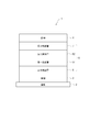
- FIG. 1 schematic structure of an example of the organic EL element in 1st embodiment of this invention is shown.
- the organic EL element 1 includes a translucent substrate 2, an anode 3, a cathode 4, and a light emitting unit 5 disposed between the anode 3 and the cathode 4, and the light emitting unit 5 is in order from the anode 3 side.
- a hole transport layer 6, a first light emitting layer 51, a second light emitting layer 52, and an electron transport layer 7 are provided.
- the first light emitting layer 51 includes a first host material and a first dopant material.
- the second light emitting layer 52 includes a second host material, a third host material, and a second dopant material.
- the first host material is preferably selected from monoamine compounds, diamine compounds, triamine compounds, tetramine compounds, amine derivatives such as amine compounds substituted with a carbazole group, and compounds having a condensed aromatic ring. Among these, an amine compound substituted with a carbazole group or a compound having a condensed aromatic ring is preferable. As the amine derivative, compounds represented by the following formulas (1) to (7) are preferable.
- Ar 1 to Ar 4 each represents a substituted or unsubstituted aromatic hydrocarbon group having 6 to 40 ring carbon atoms, or a substituted or unsubstituted aromatic group having 5 to 40 ring atoms. It is a heterocyclic group.
- the aromatic hydrocarbon group include a phenyl group, a biphenyl group, a terphenyl group, a naphthyl group, a 9,9′-dimethylfluorene group, and a phenanthrene group.
- Aromatic heterocyclic groups include thiophene monovalent residues, benzothiophene monovalent residues, dibenzothiophene monovalent residues, furan monovalent residues, benzofuran monovalent residues, dibenzofuran monovalent residues. Groups and the like.
- Ar 5 to Ar 16 are each a substituted or unsubstituted aromatic hydrocarbon group having 6 to 40 ring carbon atoms, or a substituted or unsubstituted ring atom having 5 to 40 ring atoms.
- An aromatic heterocyclic group is a substituted or unsubstituted aromatic hydrocarbon group having 6 to 40 ring carbon atoms, or a substituted or unsubstituted ring atom having 5 to 40 ring atoms.
- an aromatic amino group as a substituent an aromatic hydrocarbon group having 8 to 40 ring carbon atoms which may further have a substituent, and an aromatic heterocyclic group as a substituent; Any of the aromatic hydrocarbon groups having 8 to 40 ring atoms which may have a substituent is preferable.
- r1, r6 to r8, r11, r12, r19, r20, r23 represent integers of 1 to 4, and r9, r10, r13 to r15, r18, r21, r22 are 1 Represents an integer of ⁇ 3.
- Ar 1 to Ar 16 may be a ladder-type furan group.
- L 1 to L 7 are a single bond or a linking group having 1 to 30 carbon atoms.
- L 1 is a single bond is a structure in which an N atom and a phenylene ring are directly bonded.
- R 1 to R 23 are each a hydrogen atom, a halogen atom, a substituted or unsubstituted alkyl group having 1 to 40 carbon atoms, or a substituted or unsubstituted ring forming atom number of 5 to 40.
- An aromatic heterocyclic group a substituted or unsubstituted aromatic hydrocarbon group having 6 to 40 carbon atoms, a substituted or unsubstituted aralkyl group having 7 to 20 carbon atoms, a substituted or unsubstituted carbon group having 2 to 40 carbon atoms Alkenyl group, substituted or unsubstituted alkylamino group having 1 to 40 carbon atoms, substituted or unsubstituted aralkylamino group having 7 to 60 carbon atoms, substituted or unsubstituted alkylsilyl group having 3 to 20 carbon atoms, substituted or unsubstituted And an arylsilyl group having 8 to 40 carbon atoms, a substituted or unsubstituted aralkylsilyl group having 8 to 40 carbon atoms, and a substituted or unsubstituted alkyl halide group having 1 to 40 carbon atoms.
- X 1 to X 6 are each a sulfur atom, an oxygen atom, or an N atom substituted by a monoaromatic hydrocarbon group.
- the phenylene group directly bonded to the N atom directly bonded to Ar 1 and Ar 2 may be further directly bonded to Ar 1 or Ar 2 .
- the phenylene group directly bonded to the N atom directly bonded to Ar 3 and Ar 4 may be further directly bonded to Ar 3 or Ar 4 .
- Ar 2 and Ar 3 are preferably condensed aromatic hydrocarbons having 6 to 40 ring carbon atoms.
- Ar 2 and Ar 3 are preferably a naphthyl group.
- the phenylene group bonded via L 1 to the N atom directly bonded to Ar 5 and Ar 6 may be further directly bonded to Ar 5 or Ar 6 .
- ring-forming carbon means a carbon atom constituting a saturated ring, an unsaturated ring, or an aromatic ring.
- Ring-forming atom means a carbon atom and a hetero atom constituting a hetero ring (including a saturated ring, an unsaturated ring, and an aromatic ring).
- aromatic hydrocarbon group includes not only a non-condensed aromatic hydrocarbon group but also a condensed aromatic hydrocarbon group unless otherwise specified.
- aromatic heterocyclic group includes not only a non-condensed aromatic heterocyclic group but also a condensed aromatic heterocyclic group.
- substituents include aromatic hydrocarbon groups, heterocyclic groups, alkyl groups (straight chain or branched chain alkyl groups, cycloalkyl groups, alkyl halides). Group), alkenyl group, alkynyl group, alkylsilyl group, arylsilyl group, alkoxy group, halogenated alkoxy group, aralkyl group, aryloxy group, halogen atom, cyano group, hydroxyl group, nitro group, carboxy group, etc. Can be mentioned.
- an aromatic hydrocarbon group, a heterocyclic group, an alkyl group, a halogen atom, an alkylsilyl group, an arylsilyl group, and a cyano group are preferable, and more preferable in the description of each substituent.
- the specific substituents are preferred.
- these substituents may be further substituted with the above-mentioned substituents.
- “Unsubstituted” in the case of “substituted or unsubstituted” means that a hydrogen atom is substituted.
- the hydrogen atom includes isotopes having different numbers of neutrons, that is, light hydrogen (protium), deuterium (triuterium), and tritium.
- the amine derivatives represented by the above general formulas (1) to (7) are preferable, and compounds having a carbazolyl group Is preferred.
- Examples of the amine derivative include the following compounds.
- Examples of the compound having a condensed aromatic ring include a compound in which a substituted or unsubstituted condensed aromatic ring and a substituted or unsubstituted aromatic ring are linked.
- a compound selected from the group consisting of polycyclic aromatic compounds represented by the following formulas (10A), (10B) and (10C) is preferable.
- Ra-Ar 101 -Rb (10A) Ra-Ar 101 -Ar 102 -Rb (10B) Ra-Ar 101 -Ar 102 -Ar 103 -Rb (10C)
- Ar 101 , Ar 102 , Ar 103 , Ra and Rb are substituted or unsubstituted aromatic hydrocarbon groups having 6 to 60 ring carbon atoms.
- Ar 101 , Ar 102 , Ar 103 , Ra and Rb are substituted or unsubstituted benzene rings, A substituted or unsubstituted naphthalene ring, A substituted or unsubstituted chrysene ring, A substituted or unsubstituted fluoranthene ring, A substituted or unsubstituted phenanthrene ring, Substituted or unsubstituted benzophenanthrene ring, A substituted or unsubstituted dibenzophenanthrene ring, A substituted or unsubstituted triphenylene ring, A substituted or unsubstituted benzo [a] triphenylene ring, A substituted or unsubstituted benzochrysene ring, A substituted or unsubstituted benzo [b] fluoranthene ring, A substituted or unsubstituted fluorene ring, and It
- Ra and Rb are substituted or unsubstituted phenanthrene ring, substituted or unsubstituted benzo [c] phenanthrene ring, substituted or unsubstituted It is preferably selected from the group consisting of a triphenylene ring and a substituted or unsubstituted fluoranthene ring.
- the compound having a condensed aromatic ring may be a compound in which a substituted or unsubstituted condensed aromatic ring and a substituted or unsubstituted condensed aromatic heterocyclic ring are linked.
- the condensed aromatic heterocycle include a carbazole ring and a dibenzofuran ring.
- Specific examples of the compound having a condensed aromatic ring include the following compounds.
- the triplet energy (Eg (T)) of the first host material is preferably 2.4 eV or more, and more preferably 2.5 eV or more.
- the triplet energy of the first host material can be made larger than the triplet energy of the first dopant material.
- the triplet energy (Eg (T)) of the first host material is smaller than the triplet energy (Eg (T)) of the hole transport material of the hole transport layer 6 adjacent to the first light emitting layer 51. preferable.
- the triplet energy means an energy difference between the lowest excited triplet state and the ground state.
- the difference between Ip (ionization potential) of the first host material and Ip of the material of the hole transport layer 6 adjacent to the first light emitting layer 51 is preferably 0.2 eV or less, and 0.15 eV or less. More preferably, it is particularly preferably 0.10 eV or less. Since the difference in Ip between the first host material and the material of the hole transport layer 6 is 0.2 eV or less, the transportability of holes flowing from the hole transport layer 6 to the first light emitting layer 51 is improved. The number of holes flowing into the first light emitting layer 51 and the second light emitting layer 52 can be increased.
- the first dopant material is a phosphorescent material, and is preferably a metal complex.
- the metal complex contains at least one of iridium (Ir), palladium (Pd), and platinum (Pt). It is preferable to include.
- the metal complex is more preferably an orthometalated complex represented by the formula (20).
- a 31 is a ring bonded to A 32 and Q, and is a substituted or unsubstituted aromatic hydrocarbon group or a substituted or unsubstituted aromatic heterocyclic group.
- aromatic hydrocarbon group a phenyl group, a biphenyl group, a naphthyl group, an anthryl group, etc. are preferable.
- aromatic heterocyclic group a thienyl group, a pyridyl group, a quinolyl group, an isoquinolyl group and the like are preferable.
- Examples of the substituent substituted on the aromatic hydrocarbon group or the aromatic heterocyclic group include a halogen atom, an alkyl group having 1 to 30 carbon atoms, an alkenyl group, an alkoxycarbonyl group having 1 to 30 carbon atoms, and 1 to 30 carbon atoms. Of these, an alkoxy group, an aryloxy group, a dialkylamino group, a haloalkyl group, a cyano group and the like are preferable.
- As the halogen atom a fluorine atom or the like is preferable.
- As the alkyl group having 1 to 30 carbon atoms a methyl group, an ethyl group and the like are preferable.
- alkenyl group a vinyl group and the like are preferable.
- alkoxycarbonyl group having 1 to 30 carbon atoms a methoxycarbonyl group, an ethoxycarbonyl group and the like are preferable.
- alkoxy group having 1 to 30 carbon atoms a methoxy group, an ethoxy group, and the like are preferable.
- aryloxy group a phenoxy group, a benzyloxy group and the like are preferable.
- dialkylamino group a dimethylamino group, a diethylamino group and the like are preferable.
- acyl group an acetyl group and the like are preferable.
- a 32 is an aromatic heterocyclic group bonded to A 31 , and may contain nitrogen as an atom that forms the aromatic heterocyclic group, and may have a substituent.
- aromatic heterocyclic group a pyridyl group, pyrimidyl group, pyrazine group, triazine group, benzothiazole group, benzoxazole group, benzimidazole group, quinolyl group, isoquinolyl group, quinoxaline group, phenanthridine group and the like are preferable. Examples of the substituent which is substituted on A 32, the same as the substituent which is substituted to A 31.
- Ring containing ring and A 32 comprising A 31 is further coupled a ring structure at other sites between the ring, it may form a ring having one condensed ring or an unsaturated structure.
- Examples of such a condensed ring include a 7,8-benzoquinoline group.
- Q is any one of palladium (Pd), iridium (Ir), and platinum (Pt).
- L is a bidentate ligand.
- the bidentate ligand is preferably a ⁇ -diketo ligand such as acetylacetonate or pyromellitic acid.
- Examples of the orthometalated complex represented by the formula (20) include the following compounds.
- the first dopant material preferably exhibits an emission peak of 570 nm or more.
- the emission color showing an emission peak of 570 nm or more is, for example, red.
- the above (K-15) to (K-22), Ir (pq) 2 (acac), and Ir (tpiq) 2 (acac) are preferable.
- the second light emitting layer includes a second host material, a third host material, and a second dopant material.
- the second host material preferably has a larger affinity and ionization potential than the first host material.
- the first light-emitting layer 51 can function as an electron barrier layer due to the difference in affinity.
- the second light emitting layer 52 can also function as a hole barrier layer due to the difference in ionization potential.
- Affinity means the energy released or absorbed when one electron is given to the molecule of the host material, and is defined as positive in the case of emission and negative in the case of absorption. .
- the affinity is defined by the ionization potential (Ip) and the singlet energy (Eg (S): energy difference between the lowest excited singlet state and the ground state) as follows.
- Ip Ip-Eg (S)
- the ionization potential (Ip) means the energy required to remove ions from the compound of the host material and ionize, and was measured by, for example, an ultraviolet photoelectron spectrometer (AC-3, Riken instrument). Value.
- Singlet energy refers to the difference in optical energy between the conduction level and the valence level.
- Eg (S) Singlet energy
- the second host material and the third host material preferably satisfy the following formula (N-1) and satisfy at least one of the following formulas (N-2) and (N-3).
- Eg (S) H2 ⁇ Eg (S) H3 (N-3)
- Af H2 is the affinity of the second host material
- Af H3 is the affinity of the third host material.
- ⁇ (e) H2 is the electron mobility of the second host material
- ⁇ (e) H3 is the electron mobility of the third host material.
- Eg (S) H2 is a singlet energy of the second host material
- Eg (S) H3 is a singlet energy of the third host material.
- the emission intensity of the first light emitting layer and the second light emitting layer may be adjusted while obtaining light emission from the first light emitting layer and the second light emitting layer. For example, in order to decrease the light emission intensity of the first light emitting layer and increase the intensity of the second light emitting layer, it is necessary to move the recombination region of holes and electrons to the second light emitting layer side. The recombination region can be moved to the second light emitting layer side by weakening the electron injection of the second light emitting layer.
- the affinity Af H3 of the third host material is preferably not more than the affinity Af H2 of the second host material as shown in the formula (N-1). That is, the third host material preferably suppresses electron injection with respect to the second host material.
- the movement of the recombination region to the second light emitting layer side can also be achieved by weakening the electron transport property of the second light emitting layer.
- a third host material having a lower electron mobility than the second host material that is, a third host material satisfying the above formula (N-2) is used in the second light emitting layer.
- Add moderately the thickness of each light emitting layer can be changed or the dopant concentration can be changed. Without changing, the emission intensity of each layer can be adjusted, and an organic EL element having a desired chromaticity can be obtained.
- a third host material having a singlet energy larger than that of the second host material and a larger barrier to carriers that is, a third host material satisfying the above formula (N-3) is appropriately added to the second light emitting layer.
- the recombination region can be moved to the second light emitting layer side.
- the thickness of each light emitting layer can be changed or the dopant concentration can be changed. Without changing, the emission intensity of each layer can be adjusted, and an organic EL element having a desired chromaticity can be obtained.
- the singlet energy Eg (S) H2 of the second host material and the singlet energy Eg (S) H3 of the third host material preferably satisfy the following formula (N-31).
- ⁇ Eg (S) Eg (S) H3 ⁇ Eg (S) H2 > 0.2 [eV] (N ⁇ 31)
- the electron mobility ⁇ (e) H2 of the second host material and the electron mobility ⁇ (e) H3 of the third host material preferably satisfy the following formula (N-21).
- ⁇ (e) ⁇ (e) H2 / ⁇ (e) H3 > 10 2 cm 2 / Vs (N-21)
- the third host material if the third host material is large, the number of electrons flowing through the third host material increases, and the electron transport property of the second host material becomes weak. That is, since the electron transport property of the second host material is affected by the concentration of the third host material, the mass of the third host material relative to the total mass of the second host material and the third host material (of the third host material). By changing the (concentration), the electron transport property of the second host material can be changed, and thereby the chromaticity of the organic EL element can be adjusted.
- the mobility measurement by impedance spectroscopy will be described.
- a material to be subjected to mobility measurement having a thickness of preferably about 100 nm to 200 nm is sandwiched between the anode and the cathode, and a minute AC voltage of 100 mV or less is applied while applying a bias DC voltage.
- the AC current value (absolute value and phase) flowing at this time is measured. This measurement is performed while changing the frequency of the AC voltage, and the complex impedance (Z) is calculated from the current value and the voltage value.
- the electron mobility ⁇ (e) H2 of the second host material and the electron mobility ⁇ (e) H3 of the third host material with respect to the electron mobility ⁇ (e) H1 of the first host material of the first light emitting layer are: It is preferable that the following formula (N-4) is satisfied. ⁇ (e) H2 ⁇ ⁇ (e) H3 > ⁇ (e) H1 (N-4)
- a hole-transporting host material is used for the first light-emitting layer
- an electron-transporting host material is used for the second light-emitting layer. It is preferable to use it.
- the electron mobility is higher than that of the first host material and the second emission layer is increased. What is necessary is just to weaken the electron transport property of a 2nd light emitting layer using the 3rd host material whose electron mobility is lower than a host material.
- the hole mobility ⁇ (h) H1 of the first host material is 10 ⁇ 6 cm 2 / Vs or more
- the ionization potential Ip H1 of the first host material and the ionization potential Ip H3 of the third host material It is preferable to satisfy (N-5).
- Ip H1 ⁇ Ip H3 (N-5) since the hole transportability of the first host material is high, the performance required for the third host material is considered to be control of the hole transport ability.
- the first host material having a hole mobility ⁇ (h) H1 of 10 ⁇ 6 cm 2 / Vs or more include the amine derivatives described above.
- the affinity Af H1 of the first host material and the affinity Af H3 of the third host material are expressed by the following formula (N It is preferable to satisfy ⁇ 6).
- the performance required for the third host material is to control electrons from the second host material to the first host material.
- the third host material is preferably a compound having an electron blocking property, that is, a low affinity.
- the first host material having a hole mobility ⁇ (h) H1 smaller than 10 ⁇ 6 cm 2 / Vs include the compounds having the above-described condensed aromatic ring.
- the second host material is preferably an azine derivative.
- An azine derivative is a compound containing a six-membered ring containing one or more nitrogen atoms as a ring-forming atom (also called a nitrogen-containing six-membered heterocyclic group), a monoazine derivative, a diazine derivative, and a triazine derivative. It is preferable that it is either. Since the second host material is any one of a monoazine derivative, a diazine derivative, and a triazine derivative, the electron transport property from the electron transport layer 7 to the first light emitting layer 51 is excellent.
- the second host material is preferably a compound represented by the formulas (21) to (26), for example.
- R 101 to R 105 are any one of a substituted or unsubstituted aromatic hydrocarbon group, a substituted or unsubstituted heterocyclic group, and an alkyl group.
- an aromatic hydrocarbon group having 6 to 30 ring carbon atoms, a heterocyclic group having 5 to 30 carbon atoms, and an alkyl group having 1 to 20 carbon atoms are preferable.
- an aromatic hydrocarbon group having 6 to 30 ring carbon atoms, a heterocyclic group having 5 to 30 carbon atoms, and an alkyl group having 1 to 20 carbon atoms are preferable.
- the second host material is preferably a compound having a carbazole skeleton. Due to the second host material having a carbazole skeleton, the organic EL element 1 can be provided with no color shift and excellent durability.
- Examples of the second host material having a carbazole skeleton include compounds represented by the following general formula (BL-9) or (BL-10) (carbazole azine compounds).
- Cz is a carbazolyl group which may have a substituent or an azacarbazolyl group which may have a substituent.
- A is any group of a monoazine derivative, a diazine derivative, and a triazine derivative.
- m is an integer of 1 to 3.
- Cz represents an optionally substituted carbazolyl group or an optionally substituted azacarbazolyl group.
- A is any group of a monoazine derivative, a diazine derivative, and a triazine derivative.
- n is an integer of 1 to 3.
- the second host material having a carbazole skeleton is preferably, for example, a compound represented by the following formula (27) or (28).
- HAr 31 is a substituted or unsubstituted nitrogen-containing 6-membered heterocyclic group.
- m is any integer from 1 to 4, preferably any integer from 1 to 3, and more preferably 1 or 2.
- n is an integer from 1 to 4.
- R 31 is a substituted or unsubstituted alkyl group, or a substituted or unsubstituted aromatic hydrocarbon group.
- R 31 is a substituted or unsubstituted aromatic hydrocarbon group, a condensed ring structure in which R 31 are bonded to each other and a benzene ring is condensed may be used.
- HAr 32 is a substituted or unsubstituted nitrogen-containing 6-membered heterocyclic group.
- m is any integer from 1 to 4, preferably any integer from 1 to 3, and more preferably 1 or 2.
- n is an integer from 1 to 4.
- R 32 is a substituted or unsubstituted alkyl group or an aromatic hydrocarbon group. When R 32 is a substituted or unsubstituted aromatic hydrocarbon group, a condensed ring structure in which R 32 are bonded to each other and a benzene ring is condensed may be used.
- the second host material having a carbazole skeleton represented by the general formula (27) or (28) is a compound represented by the following formula (8) to (12A) or (29) to (32). preferable.
- Ar 101 to Ar 104 are each a hydrogen atom, a substituted or unsubstituted aromatic hydrocarbon group having 6 to 60 ring carbon atoms, and a substituted or unsubstituted ring forming atom. Any one of heterocyclic groups of 5 to 60.
- Ar 101 to Ar 104 are hydrogen atoms.
- R 110 and R 111 are the same as R 1 described above.
- n1 and n2 are any one of integers 1 to 4, and m is any one of 1 to 4.
- n2 and m are preferably any one of integers of 1 to 3, and more preferably 1 or 2. Note that the sum of n2 and m (n2 + m) has a relationship of 2 ⁇ (n2 + m) ⁇ 5.
- X is an N atom or CH, and the number of N atoms is 1 to 4.
- R 121 to R 128 are each a hydrogen atom, an aromatic hydrocarbon group, an alkyl group, or a structure in which the skeleton of the formula (12A) is linked.
- R 129 is any one of a hydrogen atom, an aromatic hydrocarbon group, and an alkyl group.
- Ar 101 to Ar 104 , R 110 , R 111 , n1, n2, and m are the same as those in the formulas (8) to (11).
- the following compounds are preferable.
- the second host material may be a compound represented by the following formula (13).
- a 1 is a substituted or unsubstituted nitrogen-containing six-membered heterocyclic group.
- a 2 is a substituted or unsubstituted aromatic hydrocarbon group having 6 to 30 ring carbon atoms or a substituted or unsubstituted nitrogen-containing heterocyclic group having 5 to 30 ring atoms.
- L 10 is a single bond or a linking group.
- a substituted or unsubstituted aromatic hydrocarbon group having 6 to 30 ring carbon atoms It is a group derived from either a substituted or unsubstituted heterocyclic group having 5 to 30 ring-forming atoms, or a group in which 2 to 5 of these groups are linked to each other.
- X 1 and X 2 are each independently a single bond, a substituted or unsubstituted aromatic hydrocarbon group having 6 to 30 ring carbon atoms, or a substituted or unsubstituted heterocyclic group having 5 to 30 ring atoms.
- One of the ring groups One of the ring groups.
- the case where X 1 is a single bond is a case where “A 1 ” and “N” adjacent to X 1 are directly bonded, and the case where X 2 is a single bond is adjacent to X 2 . In this case, “A 2 ” and “N” are directly bonded.
- Y 1 to Y 4 are each independently a hydrogen atom, a fluorine atom, a cyano group, a substituted or unsubstituted alkyl group having 1 to 20 carbon atoms, a substituted or unsubstituted alkoxy group having 1 to 20 carbon atoms, A substituted or unsubstituted haloalkyl group having 1 to 20 carbon atoms, a substituted or unsubstituted haloalkoxy group having 1 to 20 carbon atoms, a substituted or unsubstituted alkylsilyl group having 1 to 10 carbon atoms, a substituted or unsubstituted carbon Either an arylsilyl group having 6 to 30 carbon atoms, a substituted or unsubstituted aromatic hydrocarbon group having 6 to 30 ring carbon atoms, or a substituted or unsubstituted heterocyclic group having 5 to 30 ring atoms.
- adjacent Y 1 to Y 4 may form a bond with each other to form a ring structure.
- p and q are each an integer from 1 to 4
- r and s are each an integer from 1 to 3.
- the plurality of Y 1 to Y 4 may be the same or different.
- At least one of A 1 , A 2 , X 1 , X 2 , and Y 1 to Y 4 is a group derived from any of a monoazine derivative, a diazine derivative, and a triazine derivative.
- the formula (13) is preferably the following formula (13A).
- a 1 , A 2 , L 10 , X 1 , X 2 , Y 1 to Y 4 , p, q, r, and s have the same meaning as the formula (13).
- a 1 , A 2 , L 10 , X 1 , X 2 , Y 1 to Y 4 , p, q, r, and s have the same meaning as the formula (13).
- a 1 , A 2 , X 1 , X 2 , Y 1 to Y 4 , p, q, r, and s have the same meaning as the formula (13).
- Examples of the second host material of the formula (13A) include the following compounds.
- the compound of the second host material of the formula (13A) includes exemplary compounds of the second host material of the following formula (13B).
- the second host material may be a compound represented by the following formula (14) or formula (15).
- X represents a CH or N atom, and at least one of X is an N atom.
- Ar 21 to Ar 23 are each independently a substituted or unsubstituted aromatic hydrocarbon group or heterocyclic group that is not a condensed ring structure. Ar 22 or Ar 23 may form a condensed ring with the ring containing X.
- Examples of particularly preferable compounds as the second host material include the following compounds.
- the third host material of the present embodiment satisfies the relationship with the second host material described above, that is, satisfies the formula (N-1), and at least the formula (N-2) or (N-3). Any one satisfying either of them may be used.
- the third host material is preferably a compound containing a five-membered ring structure in the molecule.
- a compound having a skeleton represented by the following general formula (130) is also preferable.
- X represents an oxygen atom, a sulfur atom, NR 130 , or CR 131 R 132 .
- R 130 to R 132 are each independently a substituted or unsubstituted aromatic hydrocarbon group having 6 to 30 ring carbon atoms, or a substituted or unsubstituted heterocyclic group having 5 to 30 ring atoms. .
- a part of R 131 and R 132 may be bonded to form a ring structure.
- a compound having a skeleton represented by the above formula (130) is more preferable, and a compound having a carbazolyl group is more preferable.
- Particularly preferred is a biscarbazole derivative in which two carbazolyl groups are directly bonded.
- a preferred biscarbazole derivative as the third host material is represented by the following general formula (16).
- L 10 , X 1 , X 2 , Y 1 to Y 4 , p, q, r, and s are as defined in the general formula (13).
- B 1 and B 2 are a substituted or unsubstituted aromatic hydrocarbon group having 6 to 30 ring carbon atoms or a substituted or unsubstituted heterocyclic group having 5 to 30 ring atoms.
- Examples of preferable compounds as the third host material include the following compounds.
- the ratio of the second host material to the third host material is preferably 99: 1 to 1:99 by mass ratio, and 90:10 to 10:90. It is more preferable that the ratio is 80:20 to 20:80.
- the ratio of the second host material and the third host material (that is, the total of the host materials in the second light emitting layer) to the second dopant material is preferably 99: 1 to 50:50 by mass ratio.
- the second dopant material of this embodiment is preferably a phosphorescent metal complex.
- a 2nd dopant material of this embodiment the thing similar to what was demonstrated by the said 1st dopant material can be used. Specifically, (K-1) to (K-10), (K-12) to (K-14), (K-23) to (K-26), and Ir (Ph-ppy) 3 Is preferred.
- the second dopant material preferably exhibits an emission peak of less than 570 nm, and more preferably exhibits an emission peak of 565 nm or less. The emission color showing an emission peak of less than 570 nm is, for example, green.
- the organic EL element 1 of this embodiment is produced on a translucent substrate 2.
- This translucent substrate 2 is a substrate that supports an anode, an organic compound layer, a cathode, and the like that constitute an organic EL element, and is a smooth substrate having a light transmittance in the visible region of 400 nm to 700 nm of 50% or more. Is preferred.
- the light-transmitting substrate include a glass plate and a polymer plate.
- the glass plate include those using soda lime glass, barium / strontium-containing glass, lead glass, aluminosilicate glass, borosilicate glass, barium borosilicate glass, quartz and the like as raw materials.
- the polymer plate include those using polycarbonate, acrylic, polyethylene terephthalate, polyether sulfide, polysulfone and the like as raw materials.
- the anode of the organic EL element plays a role of injecting holes into the light emitting layer, and it is effective to have a work function of 4.5 eV or more.
- Specific examples of the anode material include indium tin oxide alloy (ITO), tin oxide (NESA), indium zinc oxide, gold, silver, platinum, and copper.
- ITO indium tin oxide alloy
- NESA tin oxide
- the light transmittance in the visible region of the anode be greater than 10%.
- the sheet resistance of the anode is preferably several hundred ⁇ / ⁇ ( ⁇ / sq. Ohm per square) or less.
- the film thickness of the anode depends on the material, it is usually selected in the range of 10 nm to 1 ⁇ m, preferably 10 nm to 200 nm.
- the cathode a material having a small work function is preferable for the purpose of injecting electrons into the light emitting layer.
- the cathode material is not particularly limited, and specifically, indium, aluminum, magnesium, magnesium-indium alloy, magnesium-aluminum alloy, aluminum-lithium alloy, aluminum-scandium-lithium alloy, magnesium-silver alloy and the like can be used.
- the cathode can be formed, for example, on the electron transport layer or the electron injection layer by a method such as vapor deposition.
- the aspect which takes out light emission from a light emitting layer from a cathode side is also employable.
- the light transmittance in the visible region of the cathode be greater than 10%.
- the sheet resistance of the cathode is preferably several hundred ⁇ / ⁇ or less.
- the thickness of the cathode depends on the material, but is usually selected in the range of 10 nm to 1 ⁇ m, preferably 50 nm to 200 nm.
- the hole injection / transport layer is a layer that assists hole injection into the light emitting layer and transports it to the light emitting region, and a compound having a high hole mobility and a low ionization energy is used.
- a material for forming the hole injecting / transporting layer a material that transports holes to the light emitting layer with lower electric field strength is preferable.
- an aromatic amine compound is preferably used.
- the electron injection / transport layer is a layer that assists injection of electrons into the light emitting layer and transports it to the light emitting region, and a compound having a high electron mobility is used.
- a compound used in the electron injecting / transporting layer for example, an aromatic heterocyclic compound containing one or more hetero atoms in the molecule is preferably used, and a nitrogen-containing ring derivative is particularly preferable.
- a nitrogen-containing ring derivative a heterocyclic compound having a nitrogen-containing 6-membered ring or 5-membered ring skeleton is preferable.
- the organic compound layer other than the first light emitting layer 51 and the second light emitting layer 52 can be arbitrarily selected from the materials used in the conventional organic EL device in addition to the compounds exemplified above. These compounds can be selected and used.
- the method for forming each layer of the organic EL element of the present embodiment is not limited except as specifically mentioned above, but a dry film forming method such as a vacuum evaporation method, a sputtering method, a plasma method, an ion plating method, a spin method, Known methods such as a coating method, a dipping method, a flow coating method, and a wet film forming method such as an ink jet method can be employed.
- the organic EL device of the present invention In manufacturing the organic EL device of the present invention, that is, the organic EL device that can easily adjust the chromaticity, as described above, first, at least the first light emitting layer and the second light emitting layer are provided between the anode and the cathode. A first host material and a first dopant material are formed on the first light emitting layer, the second light emitting layer satisfies the above formula (N-1), and A third host material that satisfies at least one of the above formulas (N-2) and (N-3) and a second dopant material may be formed. At this time, the concentration of the third host material relative to the total mass of the second host material and the third host material in the second light emitting layer may be determined by the desired chromaticity of the organic EL element.
- the organic EL element in 2nd embodiment is demonstrated.
- the organic EL element 1A of the second embodiment further includes a charge barrier layer 8 and a third light emitting layer 53 between the second light emitting layer 52 and the electron transport layer 7 in the light emitting unit 5A.
- the point provided is different from the first embodiment.
- the charge barrier layer 8 is continuously formed on the cathode 4 side of the second light emitting layer 52.
- the third light emitting layer 53 is continuously formed between the charge barrier layer 8 and the electron transport layer 7.
- the charge barrier layer 8 is formed by providing an energy barrier of the HOMO level and the LUMO level between the adjacent second light emitting layer 52 and the third light emitting layer 53, so that the charge to the second light emitting layer 52 and the third light emitting layer 53 ( This is a layer for adjusting the injection of holes or electrons and adjusting the balance of charges injected into the second light emitting layer 52 and the third light emitting layer 53.
- the third light emitting layer 53 is, for example, a layer that emits blue fluorescent light, and has a peak wavelength of 450 to 500 nm.
- the third light emitting layer 53 contains a fourth host material and a fourth dopant material. Examples of the fourth host material include compounds having a structure represented by the following formula (41) having an anthracene central skeleton.
- a 41 and A 42 are each a group derived from a substituted or unsubstituted aromatic ring having 6 to 20 nuclear carbon atoms.
- R 41 to R 48 are each a hydrogen atom, a substituted or unsubstituted aromatic hydrocarbon group having 6 to 50 nuclear carbon atoms, a substituted or unsubstituted heteroaromatic hydrocarbon group having 5 to 50 nuclear atoms, a substituted Or an unsubstituted alkyl group having 1 to 50 carbon atoms, a substituted or unsubstituted cycloalkyl group having 3 to 50 carbon atoms, a substituted or unsubstituted alkoxy group having 1 to 50 carbon atoms, a substituted or unsubstituted carbon number 6 -50 aralkyl group, substituted or unsubstituted aryloxy group having 5 to 50 nucleus atoms, substituted or unsubstituted arylthio group having 5 to 50 nucleus atom
- Examples of the substituent substituted on the aromatic ring of A 41 and A 42 include a substituted or unsubstituted aromatic hydrocarbon group having 6 to 50 nuclear carbon atoms, a substituted or unsubstituted alkyl group having 1 to 50 carbon atoms, A substituted or unsubstituted cycloalkyl group having 3 to 50 carbon atoms, a substituted or unsubstituted alkoxy group having 1 to 50 carbon atoms, a substituted or unsubstituted aralkyl group having 6 to 50 carbon atoms, a substituted or unsubstituted nucleus atom An aryloxy group having 5 to 50 atoms, a substituted or unsubstituted arylthio group having 5 to 50 nucleus atoms, a substituted or unsubstituted alkoxycarbonyl group having 1 to 50 carbon atoms, a substituted or unsubstituted silyl group, a carboxyl group, Any of
- Examples of the fourth dopant material include arylamine compounds, styrylamine compounds, anthracene, naphthalene, phenanthrene, pyrene, tetracene, coronene, chrysene, fluorescein, perylene, phthaloperylene, naphthaloperylene, perinone, phthaloperinone, naphthaloperinone, diphenylbutadiene, tetraphenyl.
- the organic EL element 1 ⁇ / b> A for example, a first dopant material that emits red light is used for the first light emitting layer 51, and a second dopant material that emits green light is used for the second light emitting layer 52.
- the organic EL element 1A can be suitably used as a surface light source such as an illumination or a backlight.
- the organic EL element of the present invention can have a tandem element configuration having at least two light emitting units.
- an intermediate layer is interposed between two light emitting units.
- the intermediate layer is a layer serving as a supply source for injecting electrons or holes into the light emitting unit, and includes an intermediate conductive layer or a charge generation layer.
- the electric charge supplied from the intermediate layer is injected into the light emitting unit. Therefore, by providing the intermediate layer, the luminous efficiency (current efficiency) with respect to the injected current is increased. improves.
- At least one of the two or more light emitting units includes at least a hole transport layer, the first light emitting layer and the second light emitting layer in the present invention, and an electron transport layer.
- any light emitting unit other than the light emitting unit including the first light emitting layer and the second light emitting layer in the present invention may be used as long as it has at least one light emitting layer.
- Specific examples of the organic EL device of the present invention are shown below.
- FIG. 3 shows an example of an organic EL element according to the third embodiment.
- the organic EL element 1B includes an anode 3, a first light emitting unit 5B1, an intermediate layer 9, a second light emitting unit 5B2, and a cathode 4.
- the first light emitting unit 5B1 includes, in order from the anode 3, a hole transport zone 6, a third light emitting layer 53, and an electron transport zone 7.
- the hole transport zone 6 includes a first hole injection layer 61 and a first hole transport layer 62.
- the third light emitting layer 53 includes a host material and a dopant material exhibiting fluorescent light having a main peak wavelength of 550 nm or less.
- the electron transport zone 7 includes a barrier layer 71 adjacent to the third light emitting layer 53 and a first electron transport layer 72.
- the second light emitting unit 5B2 is the same as the light emitting unit of the first embodiment, and the second hole transport layer 63, the first light emitting layer 51, the second light emitting layer 52, and the second electrons in order from the anode 2 side.
- the triplet energy (ETd) of the dopant material of the third light emitting layer 53 is preferably larger than the triplet energy (ETh) of the host material, and the triplet energy (ETb) of the barrier layer 71 is preferably larger than ETh. .
- Triplet excitons are confined in the third light-emitting layer 53, and the TTF phenomenon (a phenomenon in which singlet excitons are generated by collisional fusion of two triplet excitons) is efficiently caused to increase the height of the fluorescent element. It is possible to achieve efficiency.
- the barrier layer 71 refers to a layer having a barrier function against triplet energy. Therefore, the hole barrier layer and the charge barrier layer have different functions.
- the triplet energy can be measured using a commercially available apparatus F-4500 (manufactured by Hitachi). Conversion formula of triplet energy E T is as follows.
- Conversion formula E T (eV) 1239.85 / ⁇ edge
- ⁇ edge means that when the phosphorescence spectrum is expressed by taking the phosphorescence intensity on the vertical axis and the wavelength on the horizontal axis, a tangent line is drawn with respect to the rising edge on the short wavelength side of the phosphorescence spectrum. It means the wavelength value of the intersection (unit: nm).
- the intermediate layer 9 include metals, metal oxides, metal oxide mixtures, composite oxides, and electron-accepting organic compounds.
- the metal a co-deposited film of Mg, Al, Mg or Ag is preferable.
- the metal oxide include ZnO, WO 3 , MoO 3 , and MoO 2 .
- Examples of the metal oxide mixture include ITO, IZO, and ZnO: Al.
- Examples of the electron-accepting organic compound include organic compounds having a CN group as a substituent.
- a triphenylene derivative, a tetracyanoquinodimethane derivative, an indenofluorene derivative, or the like is preferable.
- the triphenylene derivative hexacyanohexaazatriphenylene (HAT) is preferable.
- As the tetracyanoquinodimethane derivative tetrafluoroquinodimethane and dicyanoquinodimethane are preferable.
- As the indenofluorene derivative compounds shown in International Publication No.
- the electron-accepting substance may be a single substance or a mixture with other organic compounds.
- Specific examples of the compound that can be used for the electron transport zone, the host material, the dopant material, and the barrier layer in the tandem device configuration of the present invention include compounds described in Japanese Patent Application Publication No. PCT / JP2010 / 003431.
- Examples of the compound that can be used in the hole transport zone include the same materials as the material of the hole transport layer of the first embodiment.
- the third light-emitting layer 53 can easily receive electrons from the charge generation layer, so that a donor represented by an alkali metal is present in the vicinity of the charge generation layer interface in the electron transport zone 7. It is preferable to dope.
- a donor metal, a donor metal compound, and a donor metal complex can be selected. Specific examples of compounds that can be used for such donor metal, donor metal compound, and donor metal complex include compounds described in Japanese Patent Application No. PCT / JP2010 / 003434.
- the present invention is not limited to the above description, and modifications within a range not departing from the gist of the present invention are included in the present invention.
- a hole injection layer may be further formed between the anode and the hole transport layer.
- a porphyrin compound an aromatic tertiary amine compound or a styrylamine compound, and in particular, an aromatic tertiary amine compound such as hexacyanohexaazatriphenylene (HAT). Is preferably used.
- the adhesion between the anode and the hole transport layer can be improved and the durability can be improved. Furthermore, by providing a hole injection layer and a hole transport layer between the anode and the first light-emitting layer, the hole transport property is compared with the case of transporting holes directly from the anode to the first light-emitting layer. Can be improved. That is, by providing a hole injection layer and a hole transport layer, an ionization potential energy difference between the anode and the hole injection layer, an ionization potential energy difference between the hole injection layer and the hole transport layer, a hole The energy difference between the ionization potentials of the transport layer and the first light emitting layer can be reduced.
- the configuration in which the electron transport layer is formed continuously with the cathode has been described.
- an electron injection layer may be further formed between the cathode and the electron transport layer.
- the configuration in which two light emitting units are formed is shown, but three or more light emitting units may be formed. In that case, a charge generation layer may be provided between the light emitting units.
- the organic EL element 1B of the third embodiment may be the organic EL element 1C shown in FIG.
- the organic EL element 1C includes an anode 3, a second light emitting unit 5B2, an intermediate layer 9, a first light emitting unit 5B1, and a cathode 4 in this order. That is, it differs from the organic EL element 1B in that the second light emitting unit 5B2 is provided on the anode 3 side and the first light emitting unit 5B1 is provided on the cathode 4 side.
- the organic EL elements of the first to third embodiments may be used as a display in addition to a surface light source such as an illumination or a backlight.
- intermediate 1-2 (2.3 g, 7.2 mmol), intermediate 1-4 (3.2 g, 8.6 mmol), tris (dibenzylideneacetone) dipalladium (0.26 g, 0.29 mmol) ), Tri-t-butylphosphonium tetrafluoroborate (0.21 g, 0.72 mmol), sodium t-butoxy (1.4 g, 14 mmol), and anhydrous xylene (40 mL) were sequentially added, and the mixture was heated to reflux for 8 hours. After cooling the reaction solution to room temperature, the organic layer was separated, and the organic solvent was distilled off under reduced pressure.
- the ionization potential was measured using an atmospheric photoelectron spectrometer (manufactured by Riken Keiki Co., Ltd .: AC-1). Specifically, the measurement was performed by irradiating the material with light and measuring the amount of electrons generated by charge separation at that time.
- Eg (S) Singlet energy
- the sample to be measured was deposited on a quartz substrate to prepare a sample, and the absorption spectrum of this sample was measured at room temperature (300K).
- the film thickness of the sample was 100 nm.
- the vertical axis represents absorbance and the horizontal axis represents wavelength.
- a tangent line was drawn with respect to the fall of the absorption spectrum on the long wavelength side, and a wavelength value ⁇ edge [nm] at the intersection of the tangent line and the horizontal axis was obtained.
- a spectrophotometer U3310 manufactured by Hitachi, Ltd. was used for the measurement of the absorption spectrum.
- the tangent with respect to the fall of the long wavelength side of an absorption spectrum was drawn as follows.
- the tangent at each point on the curve is considered. This tangent repeats as the curve falls (ie, as the value on the vertical axis decreases), the slope decreases and then increases.
- the tangent drawn at the point where the slope value takes the minimum value on the long wavelength side is taken as the tangent to the fall on the long wavelength side of the absorption spectrum.
- the maximum point whose absorbance value is 0.2 or less was not included in the maximum value on the longest wavelength side.
- Example 1 A glass substrate with an ITO transparent electrode (anode) having a thickness of 25 mm ⁇ 75 mm ⁇ 1.1 mm (manufactured by Geomatic Co., Ltd.) was subjected to ultrasonic cleaning in isopropyl alcohol for 5 minutes, and then UV ozone cleaning was performed for 30 minutes.
- the glass substrate with the transparent electrode line after cleaning is mounted on a substrate holder of a vacuum deposition apparatus, and the compound electrode HI is formed by resistance heating vapor deposition so as to cover the transparent electrode on the surface on which the transparent electrode line is formed. Were laminated. Thereby, a hole injection layer adjacent to the anode having a thickness of 20 nm was formed.
- compound HT was laminated
- the compound H1 as the first host material and the compound D1 as the first dopant material were co-evaporated by resistance heating.
- concentration of compound D1 was 8 mass%.
- the compound H2 as the second host material, the compound H3 as the third host material, and the compound D2 as the second dopant material were co-evaporated by resistance heating.
- concentration of compound D2 was 15 mass%.
- the mass (concentration) of the third host material with respect to the total mass of the second host material and the third host material in the second light emitting layer was 5 mass%.
- the compound ET was laminated by resistance heating vapor deposition. Thereby, an electron transport layer having a thickness of 35 nm was formed. Furthermore, LiF was vapor-deposited on the electron transport layer to form an electron injection layer having a thickness of 1 nm. Furthermore, metal Al was vapor-deposited on the electron injection layer to form a cathode having a thickness of 80 nm.
- Examples 2 to 4 and Comparative Examples 1 to 3 In Examples 2 to 4 and Comparative Examples 1 to 3, the film thickness of the first light emitting layer, the film thickness of the second light emitting layer, the concentration of the third host material, the third host material, and the like in Example 1 are shown in Table 2.
- An organic EL device was produced in the same manner as in Example 1 except that the changes were made as shown.
- V voltage (unit: V) when electricity was supplied between ITO and Al so that a current density might be set to 3.00 mA / cm ⁇ 2 > was measured.
- Organic EL device organic electroluminescence device 2 Substrate 3 Anode 4 Cathode 51 First light emitting layer (light emitting layer) 52 Second Light-Emitting Layer 6 Hole Transport Layer (Hole Transport Band) 61 1st hole injection layer 62 1st hole transport layer 63 2nd hole transport layer 7 Electron transport layer (electron transport zone) 72 First Electron Transport Layer 73 Second Electron Transport Layer
Landscapes
- Chemical & Material Sciences (AREA)
- Physics & Mathematics (AREA)
- Engineering & Computer Science (AREA)
- Materials Engineering (AREA)
- Optics & Photonics (AREA)
- Spectroscopy & Molecular Physics (AREA)
- Organic Chemistry (AREA)
- Electroluminescent Light Sources (AREA)
Abstract
本発明のエレクトロルミネッセンス素子は、有機陽極と陰極との間に、少なくとも第一発光層及び第二発光層を備える有機エレクトロルミネッセンス素子であって、前記第一発光層は、第一ホスト材料と、第一ドーパント材料を含み、前記第二発光層は、第二ホスト材料と第三ホスト材料と、第二ドーパント材料を含むことを特徴とする有機エレクトロルミネッセンス素子。
Description
本発明は、有機エレクトロルミネッセンス素子に関する。
有機物質を使用した有機エレクトロルミネッセンス素子(以下、有機EL素子と略記する場合がある。)は、固体発光型の安価な大面積フルカラー表示素子としての用途が有望視され、多くの開発が行われている。一般に有機EL素子は、発光層および該発光層を挟んだ一対の対向電極から構成されている。両電極間に電界が印加されると、陰極側から電子が注入され、陽極側から正孔が注入される。さらに、この電子が発光層において正孔と再結合し、励起状態を生成し、励起状態が基底状態に戻る際にエネルギーを光として放出する。
従来の有機EL素子は、無機発光ダイオードに比べて駆動電圧が高く、発光輝度や発光効率も低かった。また、特性劣化も著しかった。最近の有機EL素子は徐々に改良されているが、さらなる低電圧化、高発光効率化、長寿命化、色再現性の向上等が要求されている。
特許文献1に記載の有機EL素子は、第一発光層と第二発光層とを備え、第一発光層に含まれる第一のホスト材料は、アミン誘導体であり、第二発光層に含まれる第二のホスト材料は、モノアジン誘導体、ジアジン誘導体、およびトリアジン誘導体のいずれかである。特許文献1に記載の有機EL素子は、2つの発光層がそれぞれバランス良く発光し、その結果、低電圧で駆動し、発光効率が良好な有機EL素子となっている。
しかしながら、特許文献1に記載の有機EL素子は、2つの発光層をそれぞれバランス良く発光させるものであり、2つの発光層の発光の強度を相対的に調整して、全体の発光色を所望の色度に調整することは記載されていない。色度を変更する方法としては、各発光層の膜厚を変更することや、各発光層のドーパント濃度を変更することが考えられる。しかしながら、例えば、発光層の膜厚を薄くすると、有機EL素子の寿命が短くなるという問題がある。一方、発光層の膜厚を厚くすると、有機EL素子の駆動電圧が高くなるという問題がある。また、例えば、ドーパント濃度を高くすると、濃度消光を生じて、発光効率が低下するおそれがある。
本発明は、発光させたときの色度を調整し易い有機エレクトロルミネッセンス素子を提供することを目的とする。
本発明の一態様に係る有機エレクトロルミネッセンス素子は、陽極と陰極との間に、少なくとも第一発光層及び第二発光層を備える有機エレクトロルミネッセンス素子であって、
前記第一発光層は、第一ホスト材料と、第一ドーパント材料を含み、
前記第二発光層は、第二ホスト材料と第三ホスト材料と、第二ドーパント材料を含むことを特徴とする。
前記第一発光層は、第一ホスト材料と、第一ドーパント材料を含み、
前記第二発光層は、第二ホスト材料と第三ホスト材料と、第二ドーパント材料を含むことを特徴とする。
本発明は、発光させたときの色度を調整し易い有機エレクトロルミネッセンス素子を提供できる。
(有機EL素子の素子構成)
以下、本発明に係る有機EL素子の素子構成について説明する。
本発明の有機EL素子は、陽極と陰極との間に有機化合物層を備える。この有機化合物層は、有機化合物で構成される複数の層を有する。有機化合物層は、無機化合物を含んでいてもよい。
有機化合物層は、少なくとも第一発光層、及び第二発光層を含む複数の発光層を有する。第二発光層に対して第三発光層が隣接してもよい。
その他、正孔注入層、正孔輸送層、電子注入層、電子輸送層、正孔障壁層、電子障壁層、スペース層等の公知の有機EL素子で採用される層を有していてもよい。
以下、本発明に係る有機EL素子の素子構成について説明する。
本発明の有機EL素子は、陽極と陰極との間に有機化合物層を備える。この有機化合物層は、有機化合物で構成される複数の層を有する。有機化合物層は、無機化合物を含んでいてもよい。
有機化合物層は、少なくとも第一発光層、及び第二発光層を含む複数の発光層を有する。第二発光層に対して第三発光層が隣接してもよい。
その他、正孔注入層、正孔輸送層、電子注入層、電子輸送層、正孔障壁層、電子障壁層、スペース層等の公知の有機EL素子で採用される層を有していてもよい。
本発明の有機EL素子の素子構成としては、
(a)陽極/第一発光層/第二発光層/陰極
(b)陽極/正孔注入・輸送層/第一発光層/第二発光層/陰極
(c)陽極/第一発光層/第二発光層/電子注入・輸送層/陰極
(d)陽極/正孔注入・輸送層/第一発光層/第二発光層/電子注入・輸送層/陰極
(e)陽極/正孔注入・輸送層/第一発光層/障壁層/第二発光層/電子注入・輸送層/陰極
(f)陽極/第一発光層/第二発光層/第三発光層/陰極
(g)陽極/正孔注入・輸送層/第一発光層/第二発光層/第三発光層/陰極
(h)陽極/第三発光層/第一発光層/第二発光層/電子注入・輸送層/陰極
(i)陽極/正孔注入・輸送層/第一発光層/第二発光層/第三発光層/電子注入・輸送層/陰極
(j)陽極/正孔注入・輸送層/第一発光層/第二発光層/障壁層/電子注入・輸送層/陰極
(k)陽極/正孔注入・輸送層/第一発光層/第二発光層/障壁層/第三発光層/電子注入・輸送層/陰極
などの構造を挙げることができる。
上記の中で(d),(e),(i),(k)の構成が好ましく用いられるが、もちろんこれらに限定されるものではない。
なお、上記「発光層」とは、一般的にドーピングシステムが採用されており、ホスト材料とドーパント材料を含む有機層である。ホスト材料は、一般的に電子と正孔の再結合を促し、再結合により生じた励起エネルギーをドーパント材料に伝達させる。ドーパント材料としては、量子収率の高い化合物が好まれ、ホスト材料から励起エネルギーを受け取ったドーパント材料は、高い発光性能を示す。
また、上記「正孔注入・輸送層」は「正孔注入層および正孔輸送層のうちの少なくともいずれか1つ」を意味し、「電子注入・輸送層」は「電子注入層および電子輸送層のうちの少なくともいずれか1つ」を意味する。ここで、正孔注入層および正孔輸送層を有する場合には、陽極側に正孔注入層が設けられていることが好ましい。また、電子注入層および電子輸送層を有する場合には、陰極側に電子注入層が設けられていることが好ましい。
また、本発明において電子輸送層といった場合には、発光層と陰極との間に存在する電子注入輸送層のうち、最も電子移動度の高い有機層をいう。電子注入輸送層が一層で構成されている場合には、当該層が電子輸送層である。また、燐光素子においては、構成(i)に示すように発光層で生成された励起エネルギーの拡散を防ぐ目的で必ずしも電子移動度が高くない障壁層を発光層と電子輸送層との間に採用することがあり、発光層に隣接する有機層が電子輸送層に必ずしも該当しない。
[第一実施形態]
図1に、本発明の第一実施形態における有機EL素子の一例の概略構成を示す。
有機EL素子1は、透光性の基板2と、陽極3と、陰極4と、陽極3と陰極4との間に配置された発光ユニット5を備え、発光ユニット5は、陽極3側から順に正孔輸送層6、第一発光層51、第二発光層52、及び電子輸送層7を備える。
図1に、本発明の第一実施形態における有機EL素子の一例の概略構成を示す。
有機EL素子1は、透光性の基板2と、陽極3と、陰極4と、陽極3と陰極4との間に配置された発光ユニット5を備え、発光ユニット5は、陽極3側から順に正孔輸送層6、第一発光層51、第二発光層52、及び電子輸送層7を備える。
(発光層)
本実施形態の有機EL素子1において、第一発光層51は、第一ホスト材料および第一ドーパント材料を含んでいる。第二発光層52は、第二ホスト材料、第三ホスト材料および第二ドーパント材料を含んでいる。
本実施形態の有機EL素子1において、第一発光層51は、第一ホスト材料および第一ドーパント材料を含んでいる。第二発光層52は、第二ホスト材料、第三ホスト材料および第二ドーパント材料を含んでいる。
<第一発光層>
〔第一ホスト材料〕
第一ホスト材料は、モノアミン化合物、ジアミン化合物、トリアミン化合物、テトラミン化合物、カルバゾール基で置換されたアミン化合物などのアミン誘導体、および縮合芳香族環を有する化合物から選ばれることが好ましい。中でも、カルバゾール基で置換されたアミン化合物または縮合芳香族環を有する化合物が好ましい。
アミン誘導体としては、下記式(1)~(7)で示される化合物が好ましい。
〔第一ホスト材料〕
第一ホスト材料は、モノアミン化合物、ジアミン化合物、トリアミン化合物、テトラミン化合物、カルバゾール基で置換されたアミン化合物などのアミン誘導体、および縮合芳香族環を有する化合物から選ばれることが好ましい。中でも、カルバゾール基で置換されたアミン化合物または縮合芳香族環を有する化合物が好ましい。
アミン誘導体としては、下記式(1)~(7)で示される化合物が好ましい。


式(1)中、Ar1~Ar4は、それぞれ置換もしくは無置換の環形成炭素数6~40の芳香族炭化水素基、又は、置換もしくは無置換の環形成原子数5~40の芳香族複素環基である。
この芳香族炭化水素基としては、例えば、フェニル基、ビフェニル基、ターフェニル基、ナフチル基、9,9’-ジメチルフルオレン基、フェナントレン基などが挙げられる。
芳香族複素環基としては、チオフェンの一価残基、ベンゾチオフェンの一価残基、ジベンゾチオフェンの一価残基、フランの一価残基、ベンゾフランの一価残基、ジベンゾフランの一価残基などが挙げられる。
式(2)~(7)中、Ar5~Ar16は、それぞれ置換もしくは無置換の環形成炭素数6~40の芳香族炭化水素基、または置換もしくは無置換の環形成原子数5~40の芳香族複素環基である。置換基として芳香族アミノ基を有し、さらに置換基を有していてもよい環形成炭素数8~40の芳香族炭化水素基、及び、置換基として芳香族複素環基を有し、さらに置換基を有していてもよい環形成原子数8~40の芳香族炭化水素基のいずれかであっても好ましい。
式(1)~(7)中、r1,r6~r8,r11,r12,r19,r20,r23は、1~4の整数を表し、r9,r10,r13~r15,r18,r21,r22は1~3の整数を表す。
そして、式(1)~(7)中、Ar1~Ar16は、ラダー型フラン基でも良い。
また、式(1)~(7)中、Ar1とAr2、Ar3とAr4、Ar5とAr6、Ar8とAr9、Ar10とAr11、Ar12とAr13、Ar15とAr16は互いに結合し、環を形成しても良い。
式(2)、(4)、(6)、(7)中、L1~L7は、単結合または炭素数1~30の連結基である。
ここで、例えば、L1が単結合の場合とは、N原子とフェニレン環が直接結合した構造である。
式(1)~(7)中、R1~R23は、それぞれ水素原子、ハロゲン原子、置換もしくは無置換の炭素数1~40のアルキル基、置換もしくは無置換の環形成原子数5~40の芳香族複素環基、置換もしくは無置換の環形成炭素数6~40の芳香族炭化水素基置換もしくは無置換の炭素数7~20のアラルキル基、置換もしくは無置換の炭素数2~40のアルケニル基、置換もしくは無置換の1~40のアルキルアミノ基、置換もしくは無置換の炭素数7~60のアラルキルアミノ基、置換もしくは無置換の炭素数3~20のアルキルシリル基、置換もしくは無置換の炭素数8~40のアリールシリル基、置換もしくは無置換の炭素数8~40のアラルキルシリル基、及び置換もしくは無置換の炭素数1~40のハロゲン化アルキル基のうちのいずれかである。
式(4)、(6)、(7)中、X1~X6は、それぞれ硫黄原子、酸素原子、及びモノ芳香族炭化水素基により置換されたN原子のうちのいずれかである。
式(1)において、Ar1及びAr2に直接結合するN原子に直接結合されるフェニレン基は、さらに、Ar1またはAr2と直接結合されていてもよい。また、式(1)において、Ar3及びAr4に直接結合するN原子に直接結合されるフェニレン基は、さらに、Ar3またはAr4と直接結合されていてもよい。
そして、式(1)において、Ar2及びAr3は環形成炭素数6~40の縮合芳香族炭化水素であることが好ましい。Ar2及びAr3はさらに、ナフチル基であることが好ましい。
式(2)において、Ar5及びAr6に直接結合するN原子にL1を介して結合されるフェニレン基は、さらにAr5またはAr6と直接結合されていてもよい。
なお、本発明において、「環形成炭素」とは飽和環、不飽和環、又は芳香環を構成する炭素原子を意味する。「環形成原子」とはヘテロ環(飽和環、不飽和環、および芳香環を含む)を構成する炭素原子およびヘテロ原子を意味する。
また、「芳香族炭化水素基」には、特に指定しない限り、非縮合芳香族炭化水素基だけでなく、縮合芳香族炭化水素基も含む。「芳香族複素環基」には、特に指定しない限り、非縮合芳香族複素環基だけでなく、縮合芳香族複素環基も含む。
また、「芳香族炭化水素基」には、特に指定しない限り、非縮合芳香族炭化水素基だけでなく、縮合芳香族炭化水素基も含む。「芳香族複素環基」には、特に指定しない限り、非縮合芳香族複素環基だけでなく、縮合芳香族複素環基も含む。
また、「置換もしくは無置換の」という場合における置換基としては、上述のような芳香族炭化水素基、複素環基、アルキル基(直鎖または分岐鎖のアルキル基、シクロアルキル基、ハロゲン化アルキル基)、アルケニル基、アルキニル基、アルキルシリル基、アリールシリル基、アルコキシ基、ハロゲン化アルコキシ基、アラルキル基、アリールオキシ基、ハロゲン原子、シアノ基に加え、ヒドロキシル基、ニトロ基、カルボキシ基等が挙げられる。ここで挙げた置換基の中では、芳香族炭化水素基、複素環基、アルキル基、ハロゲン原子、アルキルシリル基、アリールシリル基、シアノ基が好ましく、さらには、各置換基の説明において好ましいとした具体的な置換基が好ましい。また、これらの置換基は、さらに上述の置換基により置換されていてもよい。
「置換もしくは無置換の」という場合における「無置換」とは、水素原子が置換したことを意味する。
以下に説明する化合物またはその部分構造において、「置換もしくは無置換の」という場合についても、上記と同様である。
本発明において、水素原子とは、中性子数が異なる同位体、すなわち、軽水素(protium)、重水素(deuterium)、三重水素(tritium)、を包含する。
「置換もしくは無置換の」という場合における「無置換」とは、水素原子が置換したことを意味する。
以下に説明する化合物またはその部分構造において、「置換もしくは無置換の」という場合についても、上記と同様である。
本発明において、水素原子とは、中性子数が異なる同位体、すなわち、軽水素(protium)、重水素(deuterium)、三重水素(tritium)、を包含する。
上記一般式(1)~(7)で表されるアミン誘導体の中でも、一般式(2)~(4)および(6)~(7)で表されるアミン誘導体が好ましく、カルバゾリル基を有する化合物が好ましい。アミン誘導体としては、例えば、以下の化合物が挙げられる。


縮合芳香族環を有する化合物としては、置換または無置換の縮合芳香族環と置換または無置換の芳香族環とが連結した化合物が挙げられる。
このような縮合芳香族環を有する化合物としては、例えば、下記式(10A)、(10B)及び(10C)で表される多環芳香族化合物からなる群から選ばれる化合物が好ましい。
このような縮合芳香族環を有する化合物としては、例えば、下記式(10A)、(10B)及び(10C)で表される多環芳香族化合物からなる群から選ばれる化合物が好ましい。
Ra-Ar101-Rb ・・・(10A)
Ra-Ar101-Ar102-Rb ・・・(10B)
Ra-Ar101-Ar102-Ar103-Rb ・・・(10C)
Ra-Ar101-Ar102-Rb ・・・(10B)
Ra-Ar101-Ar102-Ar103-Rb ・・・(10C)
前記一般式(10A)~(10C)において、Ar101,Ar102,Ar103,Ra及びRbは置換もしくは無置換の環形成炭素数6から60の芳香族炭化水素基である。
中でも、Ar101,Ar102,Ar103,Ra及びRbは
置換もしくは無置換のベンゼン環、
置換もしくは無置換のナフタレン環、
置換もしくは無置換のクリセン環、
置換もしくは無置換のフルオランテン環、
置換もしくは無置換のフェナントレン環、
置換もしくは無置換のベンゾフェナントレン環、
置換もしくは無置換のジベンゾフェナントレン環、
置換もしくは無置換のトリフェニレン環、
置換もしくは無置換のベンゾ[a]トリフェニレン環、
置換もしくは無置換のベンゾクリセン環、
置換もしくは無置換のベンゾ[b]フルオランテン環、
置換もしくは無置換のフルオレン環、及び、
置換もしくは無置換のピセン環から選択される多環芳香族骨格部を表すことが好ましい。
さらにRa及びRbの置換基は芳香族炭化水素基ではないものが好ましく、Ar101,Ar102,Ar103,Ra及びRbが同時に置換もしくは無置換のベンゼン環でないものが好ましい。
さらに、前記一般式(10A)から(10C)において、RaおよびRbのいずれか一方または両方は、置換もしくは無置換のフェナントレン環、置換もしくは無置換のベンゾ[c]フェナントレン環、置換もしくは無置換のトリフェニレン環、および置換もしくは無置換のフルオランテン環からなる群から選ばれることが好ましい。
また、縮合芳香族環を有する化合物としては、置換または無置換の縮合芳香族環と置換または無置換の縮合芳香族複素環とが連結した化合物でもよい。
縮合芳香族複素環としては、例えば、カルバゾール環およびジベンゾフラン環が挙げられる。
縮合芳香族複素環としては、例えば、カルバゾール環およびジベンゾフラン環が挙げられる。
縮合芳香族環を有する化合物の具体例としては、例えば、以下に示す化合物が挙げられる。

また、第一ホスト材料の三重項エネルギー(Eg(T))は、2.4eV以上であることが好ましく、2.5eV以上であることがさらに好ましい。第一ホスト材料の三重項エネルギーを2.4eV以上とすることにより、第一ホスト材料の三重項エネルギーを第一ドーパント材料の三重項エネルギーよりも大きな値とすることができる。これにより、第一ドーパント材料の三重項エネルギーが第一ホスト材料などに拡散することを抑制でき、発光効率等を向上させることができる。
一方、第一ホスト材料の三重項エネルギー(Eg(T))は、第一発光層51に隣接する正孔輸送層6の正孔輸送材料の三重項エネルギー(Eg(T))より小さいことが好ましい。これにより、第一発光層51に隣接する正孔輸送層6に三重項エネルギーが拡散することを避けることができ、発光効率等を向上させることができる。
なお、本発明において、三重項エネルギーとは、最低励起三重項状態と基底状態とのエネルギー差をいう。
一方、第一ホスト材料の三重項エネルギー(Eg(T))は、第一発光層51に隣接する正孔輸送層6の正孔輸送材料の三重項エネルギー(Eg(T))より小さいことが好ましい。これにより、第一発光層51に隣接する正孔輸送層6に三重項エネルギーが拡散することを避けることができ、発光効率等を向上させることができる。
なお、本発明において、三重項エネルギーとは、最低励起三重項状態と基底状態とのエネルギー差をいう。
さらに、第一ホスト材料のIp(イオン化ポテンシャル)と、第一発光層51に隣接する正孔輸送層6の材料のIpとの差を、0.2eV以下とすることが好ましく、0.15eV以下とすることがさらに好ましく、0.10eV以下とすることが特に好ましい。第一ホスト材料と正孔輸送層6の材料とのIpの差を0.2eV以下とすることにより、正孔輸送層6から第一発光層51に流れる正孔の輸送性が良好となるため、第一発光層51及び第二発光層52に流入する正孔を多くすることができる。
〔第一ドーパント材料〕
第一ドーパント材料は、燐光発光性材料であり、金属錯体であることが好ましく、当該金属錯体は、イリジウム(Ir)、パラジウム(Pd)、及び白金(Pt)のうちの少なくともいずれかの金属を含むことが好ましい。当該金属錯体は、さらに好ましくは、式(20)で示すオルトメタル化錯体である。
第一ドーパント材料は、燐光発光性材料であり、金属錯体であることが好ましく、当該金属錯体は、イリジウム(Ir)、パラジウム(Pd)、及び白金(Pt)のうちの少なくともいずれかの金属を含むことが好ましい。当該金属錯体は、さらに好ましくは、式(20)で示すオルトメタル化錯体である。

式(20)中、A31は、A32及びQと結合する環であり、置換もしくは無置換の芳香族炭化水素基又は置換もしくは無置換の芳香族複素環基である。
ここで、芳香族炭化水素基としては、フェニル基、ビフェニル基、ナフチル基、アントリル基等が好ましい。
芳香族複素環基としては、チエニル基、ピリジル基、キノリル基、イソキノリル基等が好ましい。
芳香族炭化水素基又は芳香族複素環基に置換される置換基としては、ハロゲン原子、炭素数1~30のアルキル基、アルケニル基、炭素数1~30のアルコキシカルボニル基、炭素数1~30のアルコキシ基、アリールオキシ基、ジアルキルアミノ基、ハロアルキル基、シアノ基等が好ましい。
ハロゲン原子としては、フッ素原子等が好ましい。
炭素数1~30のアルキル基としては、メチル基、エチル基等が好ましい。
アルケニル基としては、ビニル基等が好ましい。
炭素数1~30のアルコキシカルボニル基としては、メトキシカルボニル基、エトキシカルボニル基等が好ましい。
炭素数1~30のアルコキシ基としては、メトキシ基、エトキシ基等が好ましい。
アリールオキシ基としては、フェノキシ基、ベンジルオキシ基等が好ましい。
ジアルキルアミノ基としては、ジメチルアミノ基、ジエチルアミノ基等が好ましい。
アシル基としては、アセチル基等が好ましい。
ハロアルキル基としては、トリフルオロメチル基等が好ましい。
A32は、A31に結合する芳香族複素環基であり、芳香族複素環基を形成する原子として窒素を含み置換基を有していてもよい。
芳香族複素環基としては、ピリジル基、ピリミジル基、ピラジン基、トリアジン基、ベンゾチアゾール基、ベンゾオキサゾール基、ベンゾイミダゾール基、キノリル基、イソキノリル基、キノキサリン基、フェナントリジン基等が好ましい。
A32に置換される置換基としては、A31に置換される置換基と同様である。
A31を含む環とA32を含む環は、さらに環の他の部位同士で結合して環構造を結合して、一つの縮合環や不飽和構造を有する環を形成してもよい。このような縮合環としては、例えば、7,8-ベンゾキノリン基等が挙げられる。
Qは、パラジウム(Pd)、イリジウム(Ir)、及び白金(Pt)のうちのいずれかである。
Lは、2座型の配位子である。2座型の配位子としては、アセチルアセトナート等のβ-ジケト型の配位子又はピロメリット酸等が好ましい。
式(20)中、m及びnは整数を表し、Qが2価金属の場合は、n=2かつm=0であり、Qが3価金属の場合は、n=3かつm=0、又はn=2かつm=1である。
式(20)で示されるオルトメタル化錯体としては、例えば、以下の化合物が例示できる。


本実施形態において、第一ドーパント材料は、570nm以上の発光ピークを示すことが好ましい。ここで、570nm以上の発光ピークを示す発光色としては、例えば、赤色である。具体的には、上記(K-15)~(K-22)、Ir(pq)2(acac)、およびIr(tpiq)2(acac)が好ましい。
<第二発光層>
第二発光層は、第二ホスト材料と、第三ホスト材料と、第二ドーパント材料とを含む。
第二発光層は、第二ホスト材料と、第三ホスト材料と、第二ドーパント材料とを含む。
〔第一ホスト材料と第二ホスト材料との関係〕
第一発光層と第二発光層の両方から発光を得るためには、第二発光層の第二ホスト材料に電子輸送性のホスト材料を用いることが好ましい。
また、第二ホスト材料は、第一ホスト材料よりもアフィニティとイオン化ポテンシャルとが大きいことが好ましい。第二ホスト材料が、第一ホスト材料よりもアフィニティが大きい場合、そのアフィニティの差分により、第一発光層51を電子障壁層として機能させることができる。第二ホスト材料が、第一ホスト材料よりもイオン化ポテンシャルが大きい場合、そのイオン化ポテンシャルの差分により、第二発光層52を正孔障壁層としても機能させることができる。
その結果、第一発光層51と第二発光層52との界面付近で励起子を良好に生成させることができ、輝度を上昇させたとしても色ずれを抑制することができる。
なお、アフィニティ(Af、electron affinity/電子親和力)とは、ホスト材料の分子に電子を一つ与えた時に放出または吸収されるエネルギーをいい、放出の場合は正、吸収の場合は負と定義する。
アフィニティは、イオン化ポテンシャル(Ip)と一重項エネルギー(Eg(S):最低励起一重項状態と基底状態とのエネルギー差)とにより次のように規定する。
Af=Ip-Eg(S)
ここで、イオン化ポテンシャル(Ip)は、ホスト材料の化合物から電子を取り去ってイオン化するために要するエネルギーを意味し、例えば、紫外線光電子分光分析装置(AC-3、理研(株)計器)で測定した値である。
一重項エネルギー(Eg(S))は、伝導レベルと価電子レベルとの光学エネルギー差をいい、例えば、各ホスト材料のトルエン希薄溶液の吸収スペクトルの長波長側接線とベースライン(吸収ゼロ)との交点の波長値をエネルギーに換算して求める。
〔第二ホスト材料と第三ホスト材料との関係〕
第二ホスト材料と第三ホスト材料とは、下記式(N-1)を満たし、かつ下記式(N-2)および(N-3)の少なくともいずれかを満たすことが好ましい。
AfH2≧AfH3 (N-1)
μ(e)H2>μ(e)H3 (N-2)
Eg(S)H2<Eg(S)H3 (N-3)
ただし、前記式(N-1)において、AfH2は前記第二ホスト材料のアフィニティであり、AfH3は前記第三ホスト材料のアフィニティである。また、前記式(N-2)において、μ(e)H2は前記第二ホスト材料の電子移動度であり、μ(e)H3は前記第三ホスト材料の電子移動度である。前記式(N-3)において、Eg(S)H2は前記第二ホスト材料の一重項エネルギーであり、Eg(S)H3は前記第三ホスト材料の一重項エネルギーである。
有機EL素子を所望の色度とするためには、第一発光層と第二発光層とから発光を得ながら、第一発光層と第二発光層の発光強度を調整すればよい。
例えば、第一発光層の発光強度を低下させ、第二発光層の強度を増加させるためには、正孔と電子との再結合領域を第二発光層側に移動させる必要がある。再結合領域の第二発光層側への移動は、第二発光層の電子注入を弱めることにより可能となる。
本実施形態の第二発光層において、第三ホスト材料のアフィニティAfH3は、前記式(N-1)に示すように、第二ホスト材料のアフィニティAfH2以下であることが好ましい。すなわち、第三ホスト材料は、第二ホスト材料に対して電子注入を抑制することが好ましい。
例えば、第一発光層の発光強度を低下させ、第二発光層の強度を増加させるためには、正孔と電子との再結合領域を第二発光層側に移動させる必要がある。再結合領域の第二発光層側への移動は、第二発光層の電子注入を弱めることにより可能となる。
本実施形態の第二発光層において、第三ホスト材料のアフィニティAfH3は、前記式(N-1)に示すように、第二ホスト材料のアフィニティAfH2以下であることが好ましい。すなわち、第三ホスト材料は、第二ホスト材料に対して電子注入を抑制することが好ましい。
再結合領域の第二発光層側への移動は、第二発光層の電子輸送性を弱めることによっても可能となる。第二発光層の電子輸送性を弱めるためには、第二発光層に第二ホスト材料よりも電子移動度の低い第三ホスト材料、すなわち前記式(N-2)を満たす第三ホスト材料を適度に加えればよい。このように、前記式(N-1)を満たし、かつ前記式(N-2)を満たす第三ホスト材料を第二発光層に加えることにより、各発光層の膜厚の変更やドーパント濃度の変更を行うことなく、各層の発光強度を調整でき、所望の色度の有機EL素子を得ることができる。
また、第二発光層に、第二ホスト材料よりも一重項エネルギーが大きく、キャリアへの障壁が大きい第三ホスト材料、すなわち前記式(N-3)を満たす第三ホスト材料を適度に加えることでも再結合領域を第二発光層側に移動することができる。このように、前記式(N-1)を満たし、かつ前記式(N-3)を満たす第三ホスト材料を第二発光層に加えることにより、各発光層の膜厚の変更やドーパント濃度の変更を行うことなく、各層の発光強度を調整でき、所望の色度の有機EL素子を得ることができる。
さらに、第二ホスト材料の一重項エネルギーEg(S)H2と、第三ホスト材料の一重項エネルギーEg(S)H3とは、下記式(N-31)を満たすことが好ましい。
ΔEg(S)=Eg(S)H3-Eg(S)H2>0.2〔eV〕 (N-31)
また、第二ホスト材料の電子移動度μ(e)H2と、第三ホスト材料の電子移動度μ(e)H3とは、下記式(N-21)を満たすことが好ましい。
Δμ(e)=μ(e)H2/μ(e)H3>102cm2/Vs (N-21)
ΔEg(S)=Eg(S)H3-Eg(S)H2>0.2〔eV〕 (N-31)
また、第二ホスト材料の電子移動度μ(e)H2と、第三ホスト材料の電子移動度μ(e)H3とは、下記式(N-21)を満たすことが好ましい。
Δμ(e)=μ(e)H2/μ(e)H3>102cm2/Vs (N-21)
さらに、第二発光層において、第三ホスト材料が多ければ、第三ホスト材料流れる電子が多くなり、第二ホスト材料の電子輸送性が弱くなる。すなわち、第二ホスト材料の電子輸送性は、第三ホスト材料の濃度により、影響を受けるため、第二ホスト材料と第三ホスト材料の合計質量に対する第三ホスト材料の質量(第三ホスト材料の濃度)を変更することにより、第二ホスト材料の電子輸送性を変更することができ、これにより、有機EL素子の色度を調整することができる。
なお、移動度の測定方法としては、Time of Flight法等幾つかの方法が知られているが、本発明ではインピーダンス分光法で決定される移動度をいう。
インピーダンス分光法による移動度測定について説明する。陽極、陰極で好ましくは厚さ100nm~200nm程度の移動度測定の対象となる材料を挟み、バイアスDC電圧を印加しながら100mV以下の微小交流電圧を印加する。このときに流れる交流電流値(絶対値と位相)を測定する。交流電圧の周波数を変えながら本測定を行い、電流値と電圧値とから、複素インピーダンス(Z)を算出する。このときモジュラスM=iωZ(i:虚数単位、ω:角周波数)の虚数部(ImM)の周波数依存性を求め、ImMが最大値となる周波数ωの逆数を、測定対象材料の層内を伝導する電子の応答時間と定義する。そして以下の式により移動度を算出する。
移動度=(測定対象材料層の膜厚)2/(応答時間×電圧)
移動度=(測定対象材料層の膜厚)2/(応答時間×電圧)
〔第一ホスト材料、第二ホスト材料および第三ホスト材料の関係〕
第一発光層の第一ホスト材料の電子移動度μ(e)H1に対し、第二ホスト材料の電子移動度μ(e)H2および第三ホスト材料の電子移動度μ(e)H3は、下記式(N-4)を満たすことが好ましい。
μ(e)H2≧μ(e)H3>μ(e)H1 (N-4)
第一発光層の第一ホスト材料の電子移動度μ(e)H1に対し、第二ホスト材料の電子移動度μ(e)H2および第三ホスト材料の電子移動度μ(e)H3は、下記式(N-4)を満たすことが好ましい。
μ(e)H2≧μ(e)H3>μ(e)H1 (N-4)
上述したように、第一発光層と第二発光層とから発光を得るためには、第一発光層に正孔輸送性のホスト材料を用い、第二発光層に電子輸送性のホスト材料を用いることが好ましい。そして、この有機EL素子において、例えば、第一発光層の発光強度を低下させ、第二発光層の発光強度を増加させるためには、第一ホスト材料よりも電子移動度が高く、かつ第二ホスト材料よりも電子移動度が低い第三ホスト材料を用いて、第二発光層の電子輸送性を弱めればよい。
また、第一ホスト材料の正孔移動度μ(h)H1が10-6cm2/Vs以上のとき、第一ホスト材料のイオン化ポテンシャルIpH1と第三ホスト材料のイオン化ポテンシャルIpH3は下記式(N-5)を満たすことが好ましい。
IpH1<IpH3 (N-5)
この場合、第一ホスト材料の正孔輸送性が高いため、第三ホスト材料に要求される性能は正孔輸送能の制御と考えられる。一方で、第二ホスト材料に対しては正孔輸送性を有することが望ましい。
正孔移動度μ(h)H1が10-6cm2/Vs以上である第一ホスト材料としては、例えば、前述したアミン誘導体が挙げられる。
IpH1<IpH3 (N-5)
この場合、第一ホスト材料の正孔輸送性が高いため、第三ホスト材料に要求される性能は正孔輸送能の制御と考えられる。一方で、第二ホスト材料に対しては正孔輸送性を有することが望ましい。
正孔移動度μ(h)H1が10-6cm2/Vs以上である第一ホスト材料としては、例えば、前述したアミン誘導体が挙げられる。
また、第一ホスト材料の正孔移動度μ(h)H1が10-6cm2/Vsより小さいとき、第一ホスト材料のアフィニティAfH1と第三ホスト材料のアフィニティAfH3は下記式(N-6)を満たすことが好ましい。
AfH1>AfH3 (N-6)
この場合、第三ホスト材料に要求される性能は、第二ホスト材料から第一ホスト材料への電子を制御することにある。このため、第三ホスト材料は、電子ブロック性、すなわち、アフィニティの小さい化合物が望ましい。
正孔移動度μ(h)H1が10-6cm2/Vsより小さい第一ホスト材料としては、例えば、前述した縮合芳香族環を有する化合物が挙げられる。
AfH1>AfH3 (N-6)
この場合、第三ホスト材料に要求される性能は、第二ホスト材料から第一ホスト材料への電子を制御することにある。このため、第三ホスト材料は、電子ブロック性、すなわち、アフィニティの小さい化合物が望ましい。
正孔移動度μ(h)H1が10-6cm2/Vsより小さい第一ホスト材料としては、例えば、前述した縮合芳香族環を有する化合物が挙げられる。
〔第二ホスト材料〕
本実施形態において、第二ホスト材料は、アジン誘導体であることが好ましい。アジン誘導体とは、環を形成する原子として1個以上の窒素原子を含む六員環を含む化合物(含窒素六員環複素環基、ともいう)であり、モノアジン誘導体、ジアジン誘導体、及びトリアジン誘導体のうちのいずれかであることが好ましい。
第二ホスト材料がモノアジン誘導体、ジアジン誘導体、及びトリアジン誘導体のうちのいずれかであるため、電子輸送層7から第一発光層51への電子輸送性が優れる。
第二ホスト材料としては、例えば、式(21)~(26)で示される化合物であることが好ましい。
本実施形態において、第二ホスト材料は、アジン誘導体であることが好ましい。アジン誘導体とは、環を形成する原子として1個以上の窒素原子を含む六員環を含む化合物(含窒素六員環複素環基、ともいう)であり、モノアジン誘導体、ジアジン誘導体、及びトリアジン誘導体のうちのいずれかであることが好ましい。
第二ホスト材料がモノアジン誘導体、ジアジン誘導体、及びトリアジン誘導体のうちのいずれかであるため、電子輸送層7から第一発光層51への電子輸送性が優れる。
第二ホスト材料としては、例えば、式(21)~(26)で示される化合物であることが好ましい。

式(21)~(26)中、R101~R105は、置換もしくは無置換の芳香族炭化水素基、置換もしくは無置換の複素環基、及びアルキル基のうちのいずれかである。
芳香族炭化水素基に置換される置換基としては、環形成炭素数6~30の芳香族炭化水素基、炭素数5~30の複素環基、炭素数1~20のアルキル基が好ましい。
複素環基に置換される置換基としては、環形成炭素数6~30の芳香族炭化水素基、炭素数5~30の複素環基、炭素数1~20のアルキル基が好ましい。
芳香族炭化水素基に置換される置換基としては、環形成炭素数6~30の芳香族炭化水素基、炭素数5~30の複素環基、炭素数1~20のアルキル基が好ましい。
複素環基に置換される置換基としては、環形成炭素数6~30の芳香族炭化水素基、炭素数5~30の複素環基、炭素数1~20のアルキル基が好ましい。
また、第二ホスト材料は、それぞれカルバゾール骨格を有する化合物であることが好ましい。カルバゾール骨格を有する第二ホスト材料により、さらに、色ずれが生じることがなく、また耐久性にも優れた有機EL素子1とすることができる。
カルバゾール骨格を有する第二ホスト材料として、例えば、下記一般式(BL-9)又は(BL-10)で表される化合物(カルバゾールアジン系化合物)が挙げられる。
式(BL-9)中、Czは、置換基を有してもよいカルバゾリル基、又は置換基を有してもよいアザカルバゾリル基である。Aは、モノアジン誘導体、ジアジン誘導体、及びトリアジン誘導体のうちのいずれかの基である。mは1~3の整数である。
式(BL-10)中、Czは、置換基を有してもよいカルバゾリル基、又は置換基を有してもよいアザカルバゾリル基である。Aは、モノアジン誘導体、ジアジン誘導体、及びトリアジン誘導体のうちのいずれかの基である。nは1~3の整数である。
カルバゾール骨格を有する第二ホスト材料としては、例えば、下記式(27)または(28)で示される化合物であることが好ましい。
カルバゾール骨格を有する第二ホスト材料としては、例えば、下記式(27)または(28)で示される化合物であることが好ましい。

式(27)中、HAr31は、置換もしくは無置換の含窒素6員環複素環基である。mは、1~4の整数のうちのいずれかであり、好ましくは、1~3の整数のうちのいずれかであり、さらに好ましくは、1又は2である。nは、1~4の整数のうちのいずれかである。R31は、置換もしくは無置換のアルキル基、又は置換もしくは無置換の芳香族炭化水素基である。R31が置換もしくは無置換の芳香族炭化水素基である場合、R31同士が結合してベンゼン環が縮合した縮合環構造でも良い。

式(28)中、HAr32は、置換もしくは無置換の含窒素6員環複素環基である。mは、1~4の整数のうちのいずれかであり、好ましくは、1~3の整数のうちのいずれかであり、さらに好ましくは、1又は2である。nは、1~4の整数のうちのいずれかである。R32は、置換もしくは無置換のアルキル基又は芳香族炭化水素基である。R32が置換もしくは無置換の芳香族炭化水素基である場合、R32同士が結合してベンゼン環が縮合した縮合環構造でも良い。
上記一般式(27)または(28)で表されるカルバゾール骨格を有する第二ホスト材料としては、下記式(8)~(12A)または(29)~(32)で示される化合物であることが好ましい。


式(8)~(11)中、Ar101~Ar104は、それぞれ、水素原子、置換もしくは無置換の環形成炭素数6~60の芳香族炭化水素基、及び置換もしくは無置換の環形成原子数5~60の複素環基のうちのいずれかである。ただし、式(8A)、(9A)、(11A)では、Ar101~Ar103の全てが水素原子である場合はなく、式(10A)では、Ar101~Ar104の全てが水素原子である場合はない。
R110及びR111は、上記R1と同様である。
n1およびn2は、1~4の整数のうちのいずれかであり、mは、1~4の整数のうちのいずれかである。mは、好ましくは、1~3の整数のうちのいずれかであり、さらに、好ましくは、1又は2である。なお、n2とmの和(n2+m)は、2≦(n2+m)≦5の関係である。
式(12)、(12A)中、Xは、N原子又はCHであり、N原子の数は1~4である。
式(12)中、R121~R128は、それぞれ水素原子、芳香族炭化水素基、アルキル基、及び式(12A)の骨格が連結されている構造のいずれかである。
R121~R128に式(12A)の骨格が連結されている構造は、R121とR122、R122とR123、R123とR124、R125とR126、R126とR127、及びR127とR128のうちの少なくともいずれかが式(12A)の骨格に結合した構造である。
式(12A)中、R129は、水素原子、芳香族炭化水素基、及びアルキル基のうちのいずれかである。

式(29)~(32)中、Ar101~Ar104,R110,R111,n1,n2,mは、式(8)~(11)中のものと同様である。
式(29)~(32)の第二ホスト材料としては、例えば、以下の化合物が好ましい。

また、第二ホスト材料は、下記式(13)で示される化合物でもよい。

式(13)中、A1は、置換もしくは無置換の含窒素六員環複素環基である。
A2は、置換もしくは無置換の環形成炭素数が6~30の芳香族炭化水素基、又は置換もしくは無置換の環形成原子数5~30の含窒素複素環基である。
L10は、単結合または連結基である。
連結基としては、
置換もしくは無置換の環形成炭素数6~30の芳香族炭化水素基、
置換もしくは無置換の環形成原子数5~30の複素環基、または
これらの基が互いに2~5個連結した基のいずれかから誘導される基である。
なお、互いに結合した基は、互いに同一、または異なる。
X1,X2は、互いに独立して、単結合、置換もしくは無置換の環形成炭素数6~30の芳香族炭化水素基、または、置換もしくは無置換の環形成原子数5~30の複素環基のいずかである。
なお、X1が単結合の場合とは、X1に隣接する「A1」と「N」とが直接結合している場合であり、X2が単結合の場合とは、X2に隣接する「A2」と「N」とが直接結合している場合である。
Y1~Y4は、それぞれ互いに独立して、水素原子、フッ素原子、シアノ基、置換もしくは無置換の炭素数1~20のアルキル基、置換もしくは無置換の炭素数1~20のアルコキシ基、置換もしくは無置換の炭素数1~20のハロアルキル基、置換もしくは無置換の炭素数1~20のハロアルコキシ基、置換もしくは無置換の炭素数1~10のアルキルシリル基、置換もしくは無置換の炭素数6~30のアリールシリル基、置換もしくは無置換の環形成炭素数6~30の芳香族炭化水素基、または置換もしくは無置換の環形成原子数5~30の複素環基のいずれかである。なお、隣接するY1~Y4同士が互いに結合を形成し、環構造を形成しても良い。
p,qはそれぞれ1~4の整数のうちのいずれかであり、r,sはそれぞれ1~3の整数のうちのいずれかである。
なお、p,qがそれぞれ2~4の整数のうちのいずれか、r,sが2又は3の整数のいずれかの場合、複数のY1~Y4はそれぞれ同一でも異なっても良い。
A1,A2,X1,X2,及びY1~Y4のうちの少なくともいずれかは、モノアジン誘導体、ジアジン誘導体、及びトリアジン誘導体のうちのいずれかから誘導される基である。
ここで、上記式(13)は、下記式(13A)であることが好ましい。

式(13A)において、A1,A2,L10,X1,X2,Y1~Y4,p,q,r,sは前記式(13)と同義である。
また、上記式(13)は、下記式(13C)であることが好ましい。

式(13C)において、A1,A2,L10,X1,X2,Y1~Y4,p,q,r,sは前記式(13)と同義である。
また、上記式(13)は、下記式(13D)であることが好ましい。

式(13D)において、A1,A2、X1,X2,Y1~Y4,p,q,r,sは前記式(13)と同義である。
式(13A)の第二ホスト材料としては、例えば、以下の化合物が挙げられる。なお、式(13A)の第二ホスト材料の化合物には、下記式(13B)の第二ホスト材料の例示化合物も含まれる。


また、第二ホスト材料は、下記式(14)又は式(15)で示される化合物でもよい。

式(14)、(15)中、Xは、CH又はN原子を示し、Xのうち少なくとも一つは、N原子である。Ar21~Ar23は、互いに独立して縮合環構造でない置換もしくは無置換の芳香族炭化水素基又は複素環基である。
Ar22又はAr23はXを含む環と縮合環を形成してもよい。
Ar22又はAr23はXを含む環と縮合環を形成してもよい。
第二ホスト材料として、特に好ましい化合物としては、例えば以下の化合物が挙げられる。

〔第三ホスト材料〕
本実施形態の第三ホスト材料としては、前述した第二ホスト材料との関係を満たすもの、すなわち式(N-1)を満たし、かつ、式(N-2)または(N-3)の少なくともいずれかを満たすものであればよい。例えば、第一ホスト材料で説明した材料や第二ホスト材料で説明した材料のうち、前述した第二ホスト材料との関係を満たすものを挙げることができる。第三ホスト材料は、分子内に五員環構造を含む化合物が好ましい。また、下記一般式(130)で表される骨格を有する化合物でも好ましい。
本実施形態の第三ホスト材料としては、前述した第二ホスト材料との関係を満たすもの、すなわち式(N-1)を満たし、かつ、式(N-2)または(N-3)の少なくともいずれかを満たすものであればよい。例えば、第一ホスト材料で説明した材料や第二ホスト材料で説明した材料のうち、前述した第二ホスト材料との関係を満たすものを挙げることができる。第三ホスト材料は、分子内に五員環構造を含む化合物が好ましい。また、下記一般式(130)で表される骨格を有する化合物でも好ましい。

前記一般式(130)において、Xは、酸素原子、硫黄原子、NR130、またはCR131R132を表す。
R130~R132は、互いに独立して置換もしくは無置換の環形成炭素数が6~30の芳香族炭化水素基、または置換もしくは無置換の環形成原子数5~30の複素環基である。R131およびR132の一部が結合して環構造を形成していてもよい。
R130~R132は、互いに独立して置換もしくは無置換の環形成炭素数が6~30の芳香族炭化水素基、または置換もしくは無置換の環形成原子数5~30の複素環基である。R131およびR132の一部が結合して環構造を形成していてもよい。
第三ホスト材料としては、上記式(130)で表される骨格を有する化合物がより好ましく、さらに好ましくは、カルバゾリル基を有する化合物である。特に好ましくは、2つのカルバゾリル基が直接結合したビスカルバゾール誘導体である。第三ホスト材料として好ましいビスカルバゾール誘導体は、下記一般式(16)で表される。

前記一般式(16)において、L10,X1,X2,Y1~Y4,p,q,r,sは前記一般式(13)と同義である。B1およびB2は、置換もしくは無置換の環形成炭素数6~30の芳香族炭化水素基、又は置換もしくは無置換の環形成原子数5~30の複素環基である。
第三ホスト材料として、好ましい化合物としては、例えば以下に示す化合物が挙げられる。

なお、本実施形態の第二発光層において、上記第二ホスト材料と第三ホスト材料との比率は、質量比で99:1~1:99であることが好ましく、90:10~10:90であることがより好ましく、80:20~20:80であることがさらに好ましい。また、第二ホスト材料および第三ホスト材料(すなわち、第二発光層におけるホスト材料の合計)と第二ドーパント材料との比率は、質量比で99:1~50:50であることが好ましい。
〔第二ドーパント材料〕
本実施形態の第二ドーパント材料は、燐光発光性の金属錯体が好ましい。本実施形態の第二ドーパント材料としては、上記第一ドーパント材料で説明したものと同様のものを用いることができる。具体的には、上記(K-1)~(K-10)、(K-12)~(K-14)、(K-23)~(K-26)、およびIr(Ph-ppy)3が好ましい。
第二ドーパント材料としては、570nm未満の発光ピークを示すことが好ましく、565nm以下の発光ピークを示すことがさらに好ましい。570nm未満の発光ピークを示す発光色としては、例えば、緑色である。
本実施形態の第二ドーパント材料は、燐光発光性の金属錯体が好ましい。本実施形態の第二ドーパント材料としては、上記第一ドーパント材料で説明したものと同様のものを用いることができる。具体的には、上記(K-1)~(K-10)、(K-12)~(K-14)、(K-23)~(K-26)、およびIr(Ph-ppy)3が好ましい。
第二ドーパント材料としては、570nm未満の発光ピークを示すことが好ましく、565nm以下の発光ピークを示すことがさらに好ましい。570nm未満の発光ピークを示す発光色としては、例えば、緑色である。
(基板)
本実施形態の有機EL素子1は、透光性の基板2上に作製する。この透光性の基板2は、有機EL素子を構成する陽極、有機化合物層、陰極等を支持する基板であり、400nm以上700nm以下の可視領域の光の透過率が50%以上で平滑な基板が好ましい。
透光性の基板としては、ガラス板やポリマー板などが挙げられる。
ガラス板としては、特にソーダ石灰ガラス、バリウム・ストロンチウム含有ガラス、鉛ガラス、アルミノケイ酸ガラス、ホウケイ酸ガラス、バリウムホウケイ酸ガラス、石英などを原料として用いてなるものを挙げられる。
またポリマー板としては、ポリカーボネート、アクリル、ポリエチレンテレフタレート、ポリエーテルサルファイド、ポリサルフォンなどを原料として用いてなるものを挙げることができる。
(陽極および陰極)
有機EL素子の陽極は、正孔を発光層に注入する役割を担うものであり、4.5eV以上の仕事関数を有することが効果的である。
陽極材料の具体例としては、酸化インジウム錫合金(ITO)、酸化錫(NESA)、酸化インジウム亜鉛酸化物、金、銀、白金、銅などが挙げられる。
発光層からの発光を陽極側から取り出す場合、陽極の可視領域の光の透過率を10%より大きくすることが好ましい。また、陽極のシート抵抗は、数百Ω/□(Ω/sq。オーム・パー・スクウェア。)以下が好ましい。陽極の膜厚は、材料にもよるが、通常10nm以上1μm以下、好ましくは10nm以上200nm以下の範囲で選択される。
有機EL素子の陽極は、正孔を発光層に注入する役割を担うものであり、4.5eV以上の仕事関数を有することが効果的である。
陽極材料の具体例としては、酸化インジウム錫合金(ITO)、酸化錫(NESA)、酸化インジウム亜鉛酸化物、金、銀、白金、銅などが挙げられる。
発光層からの発光を陽極側から取り出す場合、陽極の可視領域の光の透過率を10%より大きくすることが好ましい。また、陽極のシート抵抗は、数百Ω/□(Ω/sq。オーム・パー・スクウェア。)以下が好ましい。陽極の膜厚は、材料にもよるが、通常10nm以上1μm以下、好ましくは10nm以上200nm以下の範囲で選択される。
陰極としては、発光層に電子を注入する目的で、仕事関数の小さい材料が好ましい。
陰極材料は特に限定されないが、具体的にはインジウム、アルミニウム、マグネシウム、マグネシウム-インジウム合金、マグネシウム-アルミニウム合金、アルミニウム-リチウム合金、アルミニウム-スカンジウム-リチウム合金、マグネシウム-銀合金などが使用できる。
陰極も、陽極と同様に、蒸着法などの方法で、例えば、電子輸送層や電子注入層上に薄膜を形成できる。また、陰極側から、発光層からの発光を取り出す態様を採用することもできる。発光層からの発光を陰極側から取り出す場合、陰極の可視領域の光の透過率を10%より大きくすることが好ましい。
陰極のシート抵抗は、数百Ω/□以下が好ましい。
陰極の膜厚は、材料にもよるが、通常10nm以上1μm以下、好ましくは50nm以上200nm以下の範囲で選択される。
(正孔注入・輸送層)
正孔注入・輸送層は、発光層への正孔注入を助け、発光領域まで輸送する層であって、正孔移動度が大きく、イオン化エネルギーが小さい化合物が用いられる。
正孔注入・輸送層を形成する材料としては、より低い電界強度で正孔を発光層に輸送する材料が好ましく、例えば、芳香族アミン化合物が好適に用いられる。
正孔注入・輸送層は、発光層への正孔注入を助け、発光領域まで輸送する層であって、正孔移動度が大きく、イオン化エネルギーが小さい化合物が用いられる。
正孔注入・輸送層を形成する材料としては、より低い電界強度で正孔を発光層に輸送する材料が好ましく、例えば、芳香族アミン化合物が好適に用いられる。
(電子注入・輸送層)
電子注入・輸送層は、発光層への電子の注入を助け、発光領域まで輸送する層であって、電子移動度が大きい化合物が用いられる。
電子注入・輸送層に用いられる化合物としては、例えば、分子内にヘテロ原子を1個以上含有する芳香族ヘテロ環化合物が好ましく用いられ、特に含窒素環誘導体が好ましい。含窒素環誘導体としては、含窒素6員環もしくは5員環骨格を有する複素環化合物が好ましい。
電子注入・輸送層は、発光層への電子の注入を助け、発光領域まで輸送する層であって、電子移動度が大きい化合物が用いられる。
電子注入・輸送層に用いられる化合物としては、例えば、分子内にヘテロ原子を1個以上含有する芳香族ヘテロ環化合物が好ましく用いられ、特に含窒素環誘導体が好ましい。含窒素環誘導体としては、含窒素6員環もしくは5員環骨格を有する複素環化合物が好ましい。
本実施形態の有機EL素子において、第一発光層51および第二発光層52以外の有機化合物層には、上述の例示した化合物以外に、従来の有機EL素子において使用される材料の中から任意の化合物を選択して用いることができる。
(層形成方法)
本実施形態の有機EL素子の各層の形成方法としては、上記で特に言及した以外には制限されないが、真空蒸着法、スパッタリング法、プラズマ法、イオンプレーティング法などの乾式成膜法や、スピンコーティング法、ディッピング法、フローコーティング法、インクジェット法などの湿式成膜法などの公知の方法を採用することができる。
本実施形態の有機EL素子の各層の形成方法としては、上記で特に言及した以外には制限されないが、真空蒸着法、スパッタリング法、プラズマ法、イオンプレーティング法などの乾式成膜法や、スピンコーティング法、ディッピング法、フローコーティング法、インクジェット法などの湿式成膜法などの公知の方法を採用することができる。
(有機EL素子の製造方法)
本発明の有機EL素子、すなわち、色度の調整をし易い有機EL素子を製造するにあたっては、上述したように、まず、陽極と陰極との間に、少なくとも第一発光層及び第二発光層を設け、第一発光層には、第一ホスト材料と、第一ドーパント材料とを成膜し、第二発光層には、第二ホスト材料と、上記式(N-1)を満たし、かつ、上記式(N-2)および(N-3)の少なくともいずれかを満たす第三ホスト材料と、第二ドーパント材料とを成膜すればよい。この際、第二発光層における第二ホスト材料と第三ホスト材料との合計質量に対する第三ホスト材料の濃度は、所望する有機EL素子の色度により決定すればよい。
本発明の有機EL素子、すなわち、色度の調整をし易い有機EL素子を製造するにあたっては、上述したように、まず、陽極と陰極との間に、少なくとも第一発光層及び第二発光層を設け、第一発光層には、第一ホスト材料と、第一ドーパント材料とを成膜し、第二発光層には、第二ホスト材料と、上記式(N-1)を満たし、かつ、上記式(N-2)および(N-3)の少なくともいずれかを満たす第三ホスト材料と、第二ドーパント材料とを成膜すればよい。この際、第二発光層における第二ホスト材料と第三ホスト材料との合計質量に対する第三ホスト材料の濃度は、所望する有機EL素子の色度により決定すればよい。
〔第二実施形態〕
次に、第二実施形態における有機EL素子について説明する。
図2に示すように、第二実施形態の有機EL素子1Aは、発光ユニット5Aにおいて、第二発光層52と電子輸送層7との間に、電荷障壁層8及び第三発光層53をさらに備えた点が第一実施形態と異なる。
電荷障壁層8は、第二発光層52の陰極4側に連続して形成されている。第三発光層53は、電荷障壁層8及び電子輸送層7間に連続して形成されている。
電荷障壁層8とは、隣接する第二発光層52及び第三発光層53間でHOMOレベル、LUMOレベルのエネルギー障壁を設けることにより、第二発光層52及び第三発光層53への電荷(正孔又は電子)注入を調整し、第二発光層52及び第三発光層53に注入される電荷のバランスを調整するための層である。
第三発光層53は、例えば、青色の蛍光発光を示す層であり、ピーク波長は450~500nmである。第三発光層53は、第四ホスト材料と、第四ドーパント材料とを含有する。
第四ホスト材料としては、例えば、アントラセン中心骨格を有する下記式(41)に示す構造を有する化合物が挙げられる。

式(41)中、A41及びA42は、それぞれ置換もしくは無置換の核炭素数6~20の芳香族環から誘導される基である。
R41~R48は、それぞれ、水素原子、置換もしくは無置換の核炭素数6~50の芳香族炭化水素基、置換もしくは無置換の核原子数5~50のヘテロ芳香族炭化水素基、置換もしくは無置換の炭素数1~50のアルキル基、置換もしくは無置換の炭素数3~50のシクロアルキル基、置換もしくは無置換の炭素数1~50のアルコキシ基、置換もしくは無置換の炭素数6~50のアラルキル基、置換もしくは無置換の核原子数5~50のアリールオキシ基、置換もしくは無置換の核原子数5~50のアリールチオ基、置換もしくは無置換の炭素数1~50のアルコキシカルボニル基、置換もしくは無置換のシリル基、カルボキシル基、ハロゲン原子、シアノ基、ニトロ基、及びヒドロキシル基のうちのいずれかである。
R41~R48は、それぞれ、水素原子、置換もしくは無置換の核炭素数6~50の芳香族炭化水素基、置換もしくは無置換の核原子数5~50のヘテロ芳香族炭化水素基、置換もしくは無置換の炭素数1~50のアルキル基、置換もしくは無置換の炭素数3~50のシクロアルキル基、置換もしくは無置換の炭素数1~50のアルコキシ基、置換もしくは無置換の炭素数6~50のアラルキル基、置換もしくは無置換の核原子数5~50のアリールオキシ基、置換もしくは無置換の核原子数5~50のアリールチオ基、置換もしくは無置換の炭素数1~50のアルコキシカルボニル基、置換もしくは無置換のシリル基、カルボキシル基、ハロゲン原子、シアノ基、ニトロ基、及びヒドロキシル基のうちのいずれかである。
A41及びA42の芳香族環に置換される置換基としては、置換もしくは無置換の核炭素数6~50の芳香族炭化水素基、置換もしくは無置換の炭素数1~50のアルキル基、置換もしくは無置換の炭素数3~50のシクロアルキル基、置換もしくは無置換の炭素数1~50のアルコキシ基、置換もしくは無置換の炭素数6~50のアラルキル基、置換もしくは無置換の核原子数5~50のアリールオキシ基、置換もしくは無置換の核原子数5~50のアリールチオ基、置換もしくは無置換の炭素数1~50のアルコキシカルボニル基、置換もしくは無置換のシリル基、カルボキシル基、ハロゲン原子、シアノ基、ニトロ基、及びヒドロキシル基のうちのいずれかが挙げられる。
第四ドーパント材料としては、例えば、アリールアミン化合物、スチリルアミン化合物、アントラセン、ナフタレン、フェナントレン、ピレン、テトラセン、コロネン、クリセン、フルオレセイン、ペリレン、フタロペリレン、ナフタロペリレン、ペリノン、フタロペリノン、ナフタロペリノン、ジフェニルブタジエン、テトラフェニルブタジエン、クマリン、オキサジアゾール、アルダジン、ビスベンゾキサゾリン、ビススチリル、ピラジン、シクロペンタジエン、キノリン金属錯体、アミノキノリン金属錯体、ベンゾキノリン金属錯体、イミン、ジフェニルエチレン、ビニルアントラセン、ジアミノカルバゾール、ピラン、チオピラン、ポリメチン、メロシアニン、イミダゾールキレート化オキシノイド化合物、キナクリドン、ルブレン及び蛍光色素等が挙げられる。
有機EL素子1Aにおいて、例えば、第一発光層51に赤色に発光する第一ドーパント材料を用い第二発光層52に緑色に発光する第二ドーパント材料を用いる。この場合、これらの発光層51,52に加えて、青色に発光する第三発光層53を備えるため、素子全体として白色発光させることができる。
従って、有機EL素子1Aは、照明やバックライトなどの面光源として好適に利用できる。
従って、有機EL素子1Aは、照明やバックライトなどの面光源として好適に利用できる。
〔第三実施形態〕
本発明の有機EL素子は、発光ユニットを少なくとも2つ有するタンデム素子構成とすることができる。このようなタンデム素子構成では、2つの発光ユニットの間に中間層が介在する。
中間層は、発光ユニットに電子又は正孔を注入する供給源となる層であり、中間導電層又は電荷発生層から構成される。一対の電極から注入される電荷に加えて、中間層から供給される電荷が発光ユニット内に注入されることになるので、中間層を設けることによって、注入した電流に対する発光効率(電流効率)が向上する。
本発明の有機EL素子は、発光ユニットを少なくとも2つ有するタンデム素子構成とすることができる。このようなタンデム素子構成では、2つの発光ユニットの間に中間層が介在する。
中間層は、発光ユニットに電子又は正孔を注入する供給源となる層であり、中間導電層又は電荷発生層から構成される。一対の電極から注入される電荷に加えて、中間層から供給される電荷が発光ユニット内に注入されることになるので、中間層を設けることによって、注入した電流に対する発光効率(電流効率)が向上する。
本発明では、2以上の発光ユニットのうち少なくとも1つが少なくとも正孔輸送層と、本発明における第一発光層及び第二発光層と、電子輸送層とを備える。なお、2以上の発光ユニットのうち本発明における第一発光層と第二発光層を含む発光ユニット以外の発光ユニットは、少なくとも1つの発光層を有せば、どのようなものであってもよい。
本発明の有機EL素子の具体例を以下に示す。
(14)陽極/第一発光ユニット/中間層/第二発光ユニット/陰極
(15)陽極/第一発光ユニット/中間層/第二発光ユニット/中間層/第三発光ユニット/陰極
本発明の有機EL素子の具体例を以下に示す。
(14)陽極/第一発光ユニット/中間層/第二発光ユニット/陰極
(15)陽極/第一発光ユニット/中間層/第二発光ユニット/中間層/第三発光ユニット/陰極
図3に第三実施形態に係る有機EL素子の一例を示す。
有機EL素子1Bは、陽極3と、第一発光ユニット5B1と、中間層9と、第二発光ユニット5B2と、陰極4とを順に備える。
第一発光ユニット5B1は、陽極3から順に、正孔輸送帯域6と、第三発光層53と、電子輸送帯域7とを備える。
正孔輸送帯域6は、第一正孔注入層61と、第一正孔輸送層62とを備える。
第三発光層53は、ホスト材料と、主ピーク波長が550nm以下の蛍光発光を示すドーパント材料とを含む。
電子輸送帯域7は、第三発光層53に隣接した障壁層71と、第一電子輸送層72を有する。
第二発光ユニット5B2は、第一実施形態の発光ユニットと同様であり、陽極2側から順に第二正孔輸送層63と、第一発光層51と、第二発光層52と、第二電子輸送層73とを備える。
第三発光層53のドーパント材料の3重項エネルギー(ETd)は、ホスト材料の3重項エネルギー(ETh)より大きく、障壁層71の三重項エネルギー(ETb)は、EThよりも大きいことが好ましい。3重項励起子が第三発光層53内に閉じ込められ、TTF現象(二つの3重項励起子の衝突融合により1重項励起子が生成する現象)を効率的に起こして蛍光素子の高効率を奏することが可能となる。
ここで、障壁層71は、三重項エネルギーに対する障壁機能を有する層をいう。従って、正孔障壁層や電荷障壁層とはその機能が異なるものである。
なお、3重項エネルギーは市販の装置F-4500(日立社製)を用いて測定できる。三重項エネルギーETの換算式は以下の通りである。
換算式 ET(eV)=1239.85/λedge
「λedge」とは、縦軸に燐光強度、横軸に波長をとって、燐光スペクトルを表したときに、燐光スペクトルの短波長側の立ち上がりに対して接線を引き、その接線と横軸の交点の波長値を意味する(単位:nm)。
中間層9としては、金属、金属酸化物、金属酸化物の混合物、複合酸化物、電子受容性有機化合物が挙げられる。金属としては、Mg、Al、MgやAgの共蒸着膜等が好ましい。金属酸化物としては、ZnO、WO3、MoO3、MoO2が挙げられる。金属酸化物の混合物としては、ITOやIZO、ZnO:Al等が挙げられる。電子受容性有機化合物としては、CN基を置換基に持つ有機化合物が挙げられる。CN基を含む有機化合物としては、トリフェニレン誘導体やテトラシアノキノジメタン誘導体、インデノフルオレン誘導体等が好ましい。トリフェニレン誘導体としては、ヘキサシアノヘキサアザトリフェニレン(HAT)が好ましい。テトラシアノキノジメタン誘導体としてはテトラフルオロキノジメタン、ジシアノキノジメタンが好ましい。インデノフルオレン誘導体としては国際公開第2009/011327号、国際公開第2009/069717号又は国際公開第2010/064655号に示されるような化合物が好ましい。なお、電子受容性物質は単独物質でも、他の有機化合物と混合されたものでもよい。
本発明のタンデム素子構成における、電子輸送帯域、ホスト材料、ドーパント材料、障壁層に使用できる化合物の具体例として、特許出願番号PCT/JP2010/003431の公報に記載の化合物が挙げられる。正孔輸送帯域に使用できる化合物としては、第一実施形態の正孔輸送層の材料と同様のものが挙げられる。
また、中間層9が電荷発生層の場合、第三発光層53が電荷発生層から電子を容易に受け取れるようにするため、電子輸送帯域7における電荷発生層界面近傍にアルカリ金属で代表されるドナーをドープすることが好ましい。ドナーとしては、ドナー性金属、ドナー性金属化合物及びドナー性金属錯体のうち少なくとも一種を選ぶことができる。このようなドナー性金属、ドナー性金属化合物及びドナー性金属錯体に使用できる化合物の具体例として、特許出願番号PCT/JP2010/003434の公報に記載の化合物が挙げられる。
[実施形態の変形例]
なお、本発明は、上記の説明に限られるものではなく、本発明の趣旨を逸脱しない範囲での変更は本発明に含まれる。
第一実施形態、第二実施形態では、陽極に連続して正孔輸送層を形成する構成を示したが、陽極及び正孔輸送層間に正孔注入層をさらに形成してもよい。
このような正孔注入層の材料としては、ポルフィリン化合物、芳香族第三級アミン化合物またはスチリルアミン化合物を用いることが好ましく、特に、ヘキサシアノヘキサアザトリフェニレン(HAT)などの芳香族第三級アミン化合物を用いることが好ましい。ヘキサシアノヘキサアザトリフェニレンを用いる場合、陽極と正孔輸送層との密着性を向上させて、耐久性を向上させることができる。
さらに、陽極と第一発光層との間に、正孔注入層と正孔輸送層とを設けることで、陽極から第一発光層に直接正孔を輸送する場合と比較し、正孔輸送性を向上させることができる。
すなわち、正孔注入層と正孔輸送層とを設けることにより、陽極と正孔注入層とのイオン化ポテンシャルのエネルギー差、正孔注入層と正孔輸送層とのイオン化ポテンシャルのエネルギー差、正孔輸送層と第一発光層とのイオン化ポテンシャルのエネルギー差をそれぞれ小さくすることができる。これにより、正孔が各層に移動する際のエネルギー障壁を小さくできるので、正孔輸送性が向上し、さらに発光効率等を向上させることができる。
また、第一実施形態~第三実施形態では、陰極に連続して電子輸送層を形成する構成を示したが、陰極及び電子輸送層間に電子注入層をさらに形成してもよい。
そして、第三実施形態では、2つの発光ユニットを形成する構成を示したが、発光ユニットを3つ以上形成してもよい。その場合、各発光ユニット間に電荷発生層を設けてもよい。
また、第三実施形態の有機EL素子1Bは、図4に示す有機EL素子1Cとしてもよい。有機EL素子1Cは、陽極3と、第二発光ユニット5B2と、中間層9と、第一発光ユニット5B1と、陰極4とを順に備える。すなわち、第二発光ユニット5B2が陽極3側に設けられ、第一発光ユニット5B1が陰極4側に設けられている点で、有機EL素子1Bと異なっている。
また、第一実施形態~第三実施形態の有機EL素子は、照明やバックライトなどの面光源の他、ディスプレイとして利用してもよい。
その他、本発明の実施における具体的な構造および形状などは、本発明の目的を達成できる範囲で他の構造などとしてもよい。
以下、本発明に係る実施例を説明するが、本発明はこれらの実施例によって限定されない。
使用した化合物は、以下の通りである。
使用した化合物は、以下の通りである。

<化合物の合成>
・合成例1(化合物H3の合成)
・合成例1-1-1(中間体1-1の合成)
・合成例1(化合物H3の合成)
・合成例1-1-1(中間体1-1の合成)

アルゴン気流下、1000mLのナスフラスコに、カルバゾール(56g、334mmol)、N,N-ジメチルホルムアミド(250mL)を加えて氷浴中(塩化ナトリウム添加)にて-7℃まで冷却し、N-ブロモスクシンイミド(119g、668mmol)のN,N-ジメチルホルムアミド(200mL)溶液を滴下して、-7℃にて4時間撹拌した。
反応液に上水を加えて室温まで昇温した後、析出した固体をろ過して取り出した。トルエンにて、得られた固体の再結晶を繰り返すことによって、中間体1-1(71g、収率65%)を得た。FD-MS(フィールドディソープションマススペクトル)の分析により、中間体1と同定した。
反応液に上水を加えて室温まで昇温した後、析出した固体をろ過して取り出した。トルエンにて、得られた固体の再結晶を繰り返すことによって、中間体1-1(71g、収率65%)を得た。FD-MS(フィールドディソープションマススペクトル)の分析により、中間体1と同定した。
・合成例1-1-2(中間体1-2の合成)

アルゴン気流下、2000mLのナスフラスコに、中間体1-1(33g、102mmol)、フェニルボロン酸(27g、221mmol)、テトラキス(トリフェニルホスフィン)パラジウム(7.0g、6.1mmol)、1,2-ジメトキシエタン(600mL)、2M炭酸ナトリウム水溶液(200mL)を順次加えて8時間加熱還流した。
室温まで反応液を冷却した後、有機層を分離し、有機溶媒を減圧下留去した。得られた残差をシリカゲルカラムクロマトグラフィーにて精製し、中間体1-2(19g、収率58%)を得た。FD-MS(フィールドディソープションマススペクトル)の分析により、中間体1-2と同定した。
室温まで反応液を冷却した後、有機層を分離し、有機溶媒を減圧下留去した。得られた残差をシリカゲルカラムクロマトグラフィーにて精製し、中間体1-2(19g、収率58%)を得た。FD-MS(フィールドディソープションマススペクトル)の分析により、中間体1-2と同定した。
・合成例1-1-3(中間体1-3の合成)

中間体1-2の合成において、中間体1-1の代わりに2,4,6-トリクロロピリミジンを用いて同様の方法で合成した。FD-MS(フィールドディソープションマススペクトル)の分析により、中間体1-3と同定した。
・合成例1-1-4(中間体1-4の合成)

中間体1-2の合成において、中間体1-1の代わりに中間体1-3を用い、フェニルボロン酸の代わりに4’-(4,4,5,5-テトラメチル-1,3,2-ジオキサボロラン-2-イル)ビフェニル-4-カルボニトリルを用いて同様の方法で合成した。FD-MS(フィールドディソープションマススペクトル)の分析により、中間体1-4と同定した。
・合成例1-1-5(化合物H3の合成)

アルゴン気流下、中間体1-2(2.3g、7.2mmol)、中間体1-4(3.2g、8.6mmol)、トリス(ジベンジリデンアセトン)ジパラジウム(0.26g、0.29mmol)、トリ-t-ブチルホスホニウムテトラフルオロほう酸塩(0.21g、0.72mmol)、t-ブトキシナトリウム(1.4g、14mmol)、無水キシレン(40mL)を順次加えて8時間加熱還流した。
室温まで反応液を冷却した後、有機層を分離し、有機溶媒を減圧下留去した。得られた残渣をシリカゲルカラムクロマトグラフィーにて精製し、3.6gの黄白色固体(H3)を得た。
得られた化合物について、FD-MS(フィールドディソープションマススペクトル)、トルエン溶液中の蛍光発光極大波長FL(PhMe, λex=325nm);λmaxを以下に示す。
FDMS, calcd for C47H30N4=650, found m/z=650 (M+)
FL(PhMe, λex=325nm);λmax, 471nm
室温まで反応液を冷却した後、有機層を分離し、有機溶媒を減圧下留去した。得られた残渣をシリカゲルカラムクロマトグラフィーにて精製し、3.6gの黄白色固体(H3)を得た。
得られた化合物について、FD-MS(フィールドディソープションマススペクトル)、トルエン溶液中の蛍光発光極大波長FL(PhMe, λex=325nm);λmaxを以下に示す。
FDMS, calcd for C47H30N4=650, found m/z=650 (M+)
FL(PhMe, λex=325nm);λmax, 471nm
<化合物の評価>
まず、本実施例で使用した化合物H1,H2,H3の物性を測定した。測定方法および算出方法を以下に示すとともに、測定結果および算出結果を表1に示す。
まず、本実施例で使用した化合物H1,H2,H3の物性を測定した。測定方法および算出方法を以下に示すとともに、測定結果および算出結果を表1に示す。
・イオン化ポテンシャル
大気下光電子分光装置(理研計器(株)社製:AC-1)を用いて測定した。具体的には、材料に光を照射し、その際に電荷分離によって生じる電子量を測定することにより測定した。
大気下光電子分光装置(理研計器(株)社製:AC-1)を用いて測定した。具体的には、材料に光を照射し、その際に電荷分離によって生じる電子量を測定することにより測定した。
・一重項エネルギーEg(S)
測定対象化合物を石英基板上に蒸着して試料を作製し、常温(300K)でこの試料の吸収スペクトルを測定した。試料の膜厚は100nmとした。吸収スペクトルは、縦軸を吸光度、横軸を波長とした。この吸収スペクトルの長波長側の立ち下がりに対して接線を引き、その接線と横軸との交点の波長値λedge[nm]を求めた。この波長値を次に示す換算式でエネルギー値に換算した値をEgSとした。
換算式:Eg(S)[eV]=1239.85/λedge
吸収スペクトルの測定には、(株)日立製の分光光度計U3310を用いた。
測定対象化合物を石英基板上に蒸着して試料を作製し、常温(300K)でこの試料の吸収スペクトルを測定した。試料の膜厚は100nmとした。吸収スペクトルは、縦軸を吸光度、横軸を波長とした。この吸収スペクトルの長波長側の立ち下がりに対して接線を引き、その接線と横軸との交点の波長値λedge[nm]を求めた。この波長値を次に示す換算式でエネルギー値に換算した値をEgSとした。
換算式:Eg(S)[eV]=1239.85/λedge
吸収スペクトルの測定には、(株)日立製の分光光度計U3310を用いた。
なお、吸収スペクトルの長波長側の立ち下がりに対する接線は以下のように引いた。吸収スペクトルの極大値のうち、最も長波長側の極大値から長波長方向にスペクトル曲線上を移動する際に、曲線上の各点における接線を考える。この接線は、曲線が立ち下がるにつれ(つまり縦軸の値が減少するにつれ)、傾きが減少しその後増加することを繰り返す。傾きの値が最も長波長側(ただし、吸光度が0.1以下となる場合は除く)で極小値をとる点において引いた接線を当該吸収スペクトルの長波長側の立ち下がりに対する接線とする。
なお、吸光度の値が0.2以下の極大点は、上記最も長波長側の極大値には含めなかった。
なお、吸光度の値が0.2以下の極大点は、上記最も長波長側の極大値には含めなかった。
・三重項エネルギーEg(T)
各化合物を、公知の燐光測定法(例えば、「光化学の世界」(日本化学会編・1993)50頁付近の記載の方法)により測定した。具体的には、各化合物を溶媒に溶解(試料10[μmol/リットル]、EPA(ジエチルエーテル:イソペンタン:エタノール=5:5:5(容積比)、各溶媒は分光用グレード)し、燐光測定用試料とした。石英セルへ入れた燐光測定用試料を77[K]に冷却し、励起光を燐光測定用試料に照射し、波長を変えながら燐光強度を測定した。燐光スペクトルは、縦軸を燐光強度、横軸を波長とした。
この燐光スペクトルの短波長側の立ち上がりに対して接線を引き、その接線と横軸との交点の波長値λedge[nm]を求めた。この波長値を次に示す換算式でエネルギー値に換算した値をEgTとした。
換算式:Eg(T)[eV]=1239.85/λedge
燐光の測定には、(株)日立ハイテクノロジー製のF-4500形分光蛍光光度計本体と低温測定用オプション備品を用いた。なお、測定装置はこの限りではなく、冷却装置及び低温用容器と、励起光源と、受光装置とを組み合わせることにより、測定してもよい。
・アフィニティAf
イオン化ポテンシャルIpと一重項エネルギーEg(S)の測定値から算出した。算出式は、次のとおりである。
Af=Ip-Eg(S)
一重項エネルギーEg(S)は、ベンゼン中の吸収スペクトルの吸収端から測定した。具体的には、市販の可視・紫外分光光度計を用いて、吸収スペクトルを測定し、そのスペクトルが立ち上がり始める波長から算出した。
イオン化ポテンシャルIpと一重項エネルギーEg(S)の測定値から算出した。算出式は、次のとおりである。
Af=Ip-Eg(S)
一重項エネルギーEg(S)は、ベンゼン中の吸収スペクトルの吸収端から測定した。具体的には、市販の可視・紫外分光光度計を用いて、吸収スペクトルを測定し、そのスペクトルが立ち上がり始める波長から算出した。
・電子移動度μ(e)および正孔移動度μ(h)
インピーダンス分光法を用いて移動度評価を行った。以下のような単キャリアデバイスを作製し、100mVの交流電圧を乗せたDC電圧を印加し複素モジュラスを測定した。モジュラスの虚部が最大となる周波数をfmax(Hz)としたとき、応答時間T(秒)をT=1/2/π/fmaxとして算出し、この値を用いて移動度の電界強度依存性を決定した。以下に、正孔移動度μ(h)および電子移動度μ(e)の測定に用いた単キャリアデバイスをそれぞれ記載する。
インピーダンス分光法を用いて移動度評価を行った。以下のような単キャリアデバイスを作製し、100mVの交流電圧を乗せたDC電圧を印加し複素モジュラスを測定した。モジュラスの虚部が最大となる周波数をfmax(Hz)としたとき、応答時間T(秒)をT=1/2/π/fmaxとして算出し、この値を用いて移動度の電界強度依存性を決定した。以下に、正孔移動度μ(h)および電子移動度μ(e)の測定に用いた単キャリアデバイスをそれぞれ記載する。
μ(h):Al/測定対象化合物(150)/ET(5)/LiF(1)/Al
μ(e):ITO/HT(5)/測定対象化合物(100)/Al
(括弧内の数値は膜厚。単位:nm)。
μ(e):ITO/HT(5)/測定対象化合物(100)/Al
(括弧内の数値は膜厚。単位:nm)。

・実施例1
25mm×75mm×1.1mm厚のITO透明電極(陽極)付きガラス基板(ジオマテック(株)社製)をイソプロピルアルコール中で超音波洗浄を5分間行なった後、UVオゾン洗浄を30分間行なった。
まず、洗浄後の透明電極ライン付きガラス基板を真空蒸着装置の基板ホルダーに装着し、透明電極ラインが形成されている側の面上に前記透明電極を覆うようにして、抵抗加熱蒸着により化合物HIを積層した。これにより、厚さ20nmの陽極に隣接する正孔注入層を形成した。
この正孔注入層上に、抵抗加熱蒸着により化合物HTを積層した。これにより、厚さ30nmの正孔輸送層を形成した。
この正孔輸送層上に、第一ホスト材料としての化合物H1と、第一ドーパント材料としての化合物D1とを抵抗加熱で共蒸着した。これにより、赤発光を示す厚さ10nmの第一発光層を形成した。尚、化合物D1の濃度は、8質量%とした。
さらにこの第一発光層の上に、第二ホスト材料としての化合物H2と、第三ホスト材料としての化合物H3、第二ドーパント材料としての化合物D2とを抵抗加熱で共蒸着した。これにより、緑発光を示す厚さ30nmの第二発光層を形成した。尚、化合物D2の濃度は、15質量%とした。また、第二発光層における第二ホスト材料と第三ホスト材料との合計質量に対する第三ホスト材料の質量(濃度)は、5質量%とした。
この緑色発光層上に、抵抗加熱蒸着により化合物ETを積層した。これにより、厚さ35nmの電子輸送層を形成した。
さらに、電子輸送層上に、LiFを蒸着し、厚さ1nmの電子注入層を形成した。さらに、電子注入層上に、金属Alを蒸着し、厚さ80nmの陰極を形成した。
・実施例2~4および比較例1~3
実施例2~4および比較例1~3は、実施例1において、第一発光層の膜厚、第二発光層の膜厚、第三ホスト材料、第三ホスト材料の濃度等を表2に示すように変更した以外は、実施例1と同様にして有機EL素子を作製した。
実施例2~4および比較例1~3は、実施例1において、第一発光層の膜厚、第二発光層の膜厚、第三ホスト材料、第三ホスト材料の濃度等を表2に示すように変更した以外は、実施例1と同様にして有機EL素子を作製した。

〔有機EL素子の評価〕
実施例1~4および比較例1~3において作製した有機EL素子において、電流密度を3.00mA/cm2とした場合の駆動電圧、CIE1931色度、電流効率L/J、電力効率η、及び寿命LT90の評価を行った。結果を表3に示す。
実施例1~4および比較例1~3において作製した有機EL素子において、電流密度を3.00mA/cm2とした場合の駆動電圧、CIE1931色度、電流効率L/J、電力効率η、及び寿命LT90の評価を行った。結果を表3に示す。
・駆動電圧
電流密度が3.00mA/cm2となるようにITOとAlとの間に通電したときの電圧(単位:V)を計測した。
電流密度が3.00mA/cm2となるようにITOとAlとの間に通電したときの電圧(単位:V)を計測した。
・CIE1931色度
電流密度が3.00mA/cm2となるように素子に電圧を印加した時のCIE1931色度座標(x、y)を分光放射輝度計CS-1000(コニカミノルタ社製)で計測した。
・電流効率L/J、及び電力効率η
電流密度が3.00mA/cm2となるように素子に電圧を印加した時の分光放射輝度スペクトルを上記分光放射輝度計で計測し、得られた分光放射輝度スペクトルから、電流効率(単位:cd/A)、及び電力効率η(単位:lm/W)を算出した。
・寿命LT90
電流密度が50mA/cm2となるように素子に電圧を印加し、初期輝度に対して輝度が90%となるまでの時間(単位:hr)を測定した。
電流密度が3.00mA/cm2となるように素子に電圧を印加した時のCIE1931色度座標(x、y)を分光放射輝度計CS-1000(コニカミノルタ社製)で計測した。
・電流効率L/J、及び電力効率η
電流密度が3.00mA/cm2となるように素子に電圧を印加した時の分光放射輝度スペクトルを上記分光放射輝度計で計測し、得られた分光放射輝度スペクトルから、電流効率(単位:cd/A)、及び電力効率η(単位:lm/W)を算出した。
・寿命LT90
電流密度が50mA/cm2となるように素子に電圧を印加し、初期輝度に対して輝度が90%となるまでの時間(単位:hr)を測定した。

表2および表3から分かるように、第二発光層に第三ホスト材料H3を含む実施例1~4では、第一発光層および第二発光層の膜厚を変更することなく、第三ホスト材料H3の濃度を変更するだけで、色度CIEを変更することができる。これに対し、第二発光層に第三ホスト材料H3を含まない比較例1~3では、膜厚を変更することにより色度CIEを変更する。しかしながら、比較例1に比べて、第二発光層の膜厚を厚くした比較例2では、比較例1に比べて電圧が大きく上昇している。また比較例1に比べて、第一発光層の膜厚を薄くした比較例3では、膜厚を半分にしたにも関わらず、色度CIEに変化が見られなかった。
1,1A,1B,1C 有機EL素子(有機エレクトロルミネッセンス素子)
2 基板
3 陽極
4 陰極
51 第一発光層(発光層)
52 第二発光層
6 正孔輸送層(正孔輸送帯域)
61 第一正孔注入層
62 第一正孔輸送層
63 第二正孔輸送層
7 電子輸送層(電子輸送帯域)
72 第一電子輸送層
73 第二電子輸送層
2 基板
3 陽極
4 陰極
51 第一発光層(発光層)
52 第二発光層
6 正孔輸送層(正孔輸送帯域)
61 第一正孔注入層
62 第一正孔輸送層
63 第二正孔輸送層
7 電子輸送層(電子輸送帯域)
72 第一電子輸送層
73 第二電子輸送層
Claims (7)
- 陽極と陰極との間に、少なくとも第一発光層及び第二発光層を備える有機エレクトロルミネッセンス素子であって、
前記第一発光層は、第一ホスト材料と、第一ドーパント材料を含み
前記第二発光層は、第二ホスト材料と第三ホスト材料と、第二ドーパント材料を含むことを特徴とする有機エレクトロルミネッセンス素子。 - 請求項1に記載の有機エレクトロルミネッセンス素子において、
前記第二ホスト材料と前記第三ホスト材料とは、下記式(N-1)を満たし、かつ、下記式(N-2)および(N-3)の少なくともいずれかを満たすことを特徴とするエレクトロルミネッセンス素子。
AfH2≧AfH3 (N-1)
μ(e)H2>μ(e)H3 (N-2)
Eg(S)H2<Eg(S)H3 (N-3)
ただし、前記式(N-1)において、AfH2は前記第二ホスト材料のアフィニティであり、AfH3は前記第三ホスト材料のアフィニティである。また、前記式(N-2)において、μ(e)H2は前記第二ホスト材料の電子移動度であり、μ(e)H3は前記第三ホスト材料の電子移動度である。前記式(N-3)において、Eg(S)H2は前記第二ホスト材料の一重項エネルギーであり、Eg(S)H3は前記第三ホスト材料の一重項エネルギーである。 - 請求項1または請求項2に記載の有機エレクトロルミネッセンス素子において、
前記第二ホスト材料の一重項エネルギーEg(S)H2と、前記第三ホスト材料の一重項エネルギーEg(S)H3とは、下記式(N-31)を満たすことを特徴とする有機エレクトロルミネッセンス素子。
ΔEg(S)=Eg(S)H3-Eg(S)H2>0.2〔eV〕 (N-31) - 請求項1から請求項3までのいずれか1項に記載の有機エレクトロルミネッセンス素子において、
前記第二ホスト材料の電子移動度μ(e)H2と、前記第三ホスト材料の電子移動度μ(e)H3とは、下記式(N-21)を満たすことを特徴とする有機エレクトロルミネッセンス素子。
Δμ(e)=μ(e)H2/μ(e)H3>102cm2/Vs (N-21) - 請求項1から請求項4までのいずれか1項に記載の有機エレクトロルミネッセンス素子において、
前記第一ドーパント材料は、570nm以上の発光ピークを示し、
前記第二ドーパント材料は、570nm未満の発光ピークを示すことを特徴とする有機エレクトロルミネッセンス素子。 - 請求項1から請求項5までのいずれか1項に記載の有機エレクトロルミネッセンス素子において、
前記第二ホスト材料は、アジン誘導体であることを特徴とする有機エレクトロルミネッセンス素子。 - 請求項1から請求項6までのいずれか1項に記載の有機エレクトロルミネッセンス素子において、
前記第一発光層は、前記第二発光層よりも陽極側に設けられることを特徴とする有機エレクトロルミネッセンス素子。
Priority Applications (2)
| Application Number | Priority Date | Filing Date | Title |
|---|---|---|---|
| US14/648,790 US9647226B2 (en) | 2012-12-03 | 2013-11-28 | Organic electroluminescent element |
| US15/472,187 US20170200920A1 (en) | 2012-12-03 | 2017-03-28 | Organic electroluminescent element |
Applications Claiming Priority (2)
| Application Number | Priority Date | Filing Date | Title |
|---|---|---|---|
| JP2012-264652 | 2012-12-03 | ||
| JP2012264652A JP6133583B2 (ja) | 2012-12-03 | 2012-12-03 | 有機エレクトロルミネッセンス素子 |
Related Child Applications (2)
| Application Number | Title | Priority Date | Filing Date |
|---|---|---|---|
| US14/648,790 A-371-Of-International US9647226B2 (en) | 2012-12-03 | 2013-11-28 | Organic electroluminescent element |
| US15/472,187 Division US20170200920A1 (en) | 2012-12-03 | 2017-03-28 | Organic electroluminescent element |
Publications (1)
| Publication Number | Publication Date |
|---|---|
| WO2014087913A1 true WO2014087913A1 (ja) | 2014-06-12 |
Family
ID=50883332
Family Applications (1)
| Application Number | Title | Priority Date | Filing Date |
|---|---|---|---|
| PCT/JP2013/082030 WO2014087913A1 (ja) | 2012-12-03 | 2013-11-28 | 有機エレクトロルミネッセンス素子 |
Country Status (3)
| Country | Link |
|---|---|
| US (2) | US9647226B2 (ja) |
| JP (1) | JP6133583B2 (ja) |
| WO (1) | WO2014087913A1 (ja) |
Cited By (4)
| Publication number | Priority date | Publication date | Assignee | Title |
|---|---|---|---|---|
| WO2015156587A1 (en) * | 2014-04-08 | 2015-10-15 | Rohm And Haas Electronic Materials Korea Ltd. | Multi-component host material and organic electroluminescent device comprising the same |
| WO2022191237A1 (ja) * | 2021-03-12 | 2022-09-15 | 出光興産株式会社 | 有機エレクトロルミネッセンス素子及び電子機器 |
| WO2022191155A1 (ja) * | 2021-03-12 | 2022-09-15 | 出光興産株式会社 | 有機エレクトロルミネッセンス素子の製造方法、有機エレクトロルミネッセンス素子パネル及び電子機器 |
| WO2022191234A1 (ja) * | 2021-03-11 | 2022-09-15 | 出光興産株式会社 | 有機エレクトロルミネッセンス素子、電子機器及び有機エレクトロルミネッセンス素子の製造方法 |
Families Citing this family (9)
| Publication number | Priority date | Publication date | Assignee | Title |
|---|---|---|---|---|
| JP6133583B2 (ja) * | 2012-12-03 | 2017-05-24 | 出光興産株式会社 | 有機エレクトロルミネッセンス素子 |
| KR102523989B1 (ko) * | 2013-12-02 | 2023-04-21 | 가부시키가이샤 한도오따이 에네루기 켄큐쇼 | 발광 소자, 발광 장치, 전자 기기, 및 조명 장치 |
| KR101790726B1 (ko) * | 2015-11-20 | 2017-10-26 | 한국생산기술연구원 | 색좌표 및 색온도 조절이 가능한 탠덤 구조의 oled 소자 및 이의 색좌표 및 색온도 조절방법 |
| WO2017188655A1 (ko) * | 2016-04-26 | 2017-11-02 | 덕산네오룩스 주식회사 | 유기전기소자용 화합물, 이를 이용한 유기전기소자 및 그 전자 장치 |
| JP2020143169A (ja) * | 2017-05-25 | 2020-09-10 | 出光興産株式会社 | 組成物、有機エレクトロルミネッセンス素子用材料、組成物膜、有機エレクトロルミネッセンス素子、及び電子機器 |
| JP7102211B2 (ja) | 2018-04-26 | 2022-07-19 | キヤノン株式会社 | 有機el素子、それを有する表示装置、照明装置、移動体 |
| JP2021182459A (ja) | 2018-06-04 | 2021-11-25 | 出光興産株式会社 | 有機エレクトロルミネッセンス素子及び電子機器 |
| WO2021256565A1 (ja) * | 2020-06-19 | 2021-12-23 | 出光興産株式会社 | 有機エレクトロルミネッセンス素子及び電子機器 |
| JPWO2021256564A1 (ja) * | 2020-06-19 | 2021-12-23 |
Citations (5)
| Publication number | Priority date | Publication date | Assignee | Title |
|---|---|---|---|---|
| JP2005228737A (ja) * | 2004-01-15 | 2005-08-25 | Fuji Photo Film Co Ltd | 有機電界発光素子 |
| JP2007027092A (ja) * | 2005-07-15 | 2007-02-01 | Samsung Sdi Co Ltd | 白色有機発光素子及びその製造方法 |
| JP2010161410A (ja) * | 2002-10-09 | 2010-07-22 | Idemitsu Kosan Co Ltd | 有機エレクトロルミネッセンス素子 |
| JP2011160003A (ja) * | 2004-11-12 | 2011-08-18 | Samsung Mobile Display Co Ltd | 有機電界発光素子 |
| WO2011148909A1 (ja) * | 2010-05-24 | 2011-12-01 | 出光興産株式会社 | 有機エレクトロルミネッセンス素子 |
Family Cites Families (10)
| Publication number | Priority date | Publication date | Assignee | Title |
|---|---|---|---|---|
| US20050158582A1 (en) | 2004-01-15 | 2005-07-21 | Fuji Photo Film Co., Ltd. | Organic electroluminescent element |
| TW200908777A (en) * | 2007-03-23 | 2009-02-16 | Idemitsu Kosan Co | Organic el device |
| EP2045848B1 (en) | 2007-07-18 | 2017-09-27 | Idemitsu Kosan Co., Ltd. | Organic electroluminescent device material and organic electroluminescent device |
| EP2213662B1 (en) | 2007-11-30 | 2012-04-18 | Idemitsu Kosan Co., Ltd. | Azaindenofluorenedione derivative, organic electroluminescent device material, and organic electroluminescent device |
| WO2010064655A1 (ja) | 2008-12-03 | 2010-06-10 | 出光興産株式会社 | インデノフルオレンジオン誘導体、有機エレクトロルミネッセンス素子用材料及び有機エレクトロルミネッセンス素子 |
| US20100295027A1 (en) * | 2009-05-22 | 2010-11-25 | Idemitsu Kosan Co., Ltd. | Organic electroluminescence device |
| US20100295444A1 (en) | 2009-05-22 | 2010-11-25 | Idemitsu Kosan Co., Ltd. | Organic electroluminescence device |
| US20100295445A1 (en) | 2009-05-22 | 2010-11-25 | Idemitsu Kosan Co., Ltd. | Organic electroluminescent device |
| CN102421772B (zh) * | 2010-04-20 | 2015-11-25 | 出光兴产株式会社 | 双咔唑衍生物、有机电致发光元件用材料及使用其的有机电致发光元件 |
| JP6133583B2 (ja) * | 2012-12-03 | 2017-05-24 | 出光興産株式会社 | 有機エレクトロルミネッセンス素子 |
-
2012
- 2012-12-03 JP JP2012264652A patent/JP6133583B2/ja active Active
-
2013
- 2013-11-28 US US14/648,790 patent/US9647226B2/en active Active
- 2013-11-28 WO PCT/JP2013/082030 patent/WO2014087913A1/ja active Application Filing
-
2017
- 2017-03-28 US US15/472,187 patent/US20170200920A1/en not_active Abandoned
Patent Citations (5)
| Publication number | Priority date | Publication date | Assignee | Title |
|---|---|---|---|---|
| JP2010161410A (ja) * | 2002-10-09 | 2010-07-22 | Idemitsu Kosan Co Ltd | 有機エレクトロルミネッセンス素子 |
| JP2005228737A (ja) * | 2004-01-15 | 2005-08-25 | Fuji Photo Film Co Ltd | 有機電界発光素子 |
| JP2011160003A (ja) * | 2004-11-12 | 2011-08-18 | Samsung Mobile Display Co Ltd | 有機電界発光素子 |
| JP2007027092A (ja) * | 2005-07-15 | 2007-02-01 | Samsung Sdi Co Ltd | 白色有機発光素子及びその製造方法 |
| WO2011148909A1 (ja) * | 2010-05-24 | 2011-12-01 | 出光興産株式会社 | 有機エレクトロルミネッセンス素子 |
Cited By (4)
| Publication number | Priority date | Publication date | Assignee | Title |
|---|---|---|---|---|
| WO2015156587A1 (en) * | 2014-04-08 | 2015-10-15 | Rohm And Haas Electronic Materials Korea Ltd. | Multi-component host material and organic electroluminescent device comprising the same |
| WO2022191234A1 (ja) * | 2021-03-11 | 2022-09-15 | 出光興産株式会社 | 有機エレクトロルミネッセンス素子、電子機器及び有機エレクトロルミネッセンス素子の製造方法 |
| WO2022191237A1 (ja) * | 2021-03-12 | 2022-09-15 | 出光興産株式会社 | 有機エレクトロルミネッセンス素子及び電子機器 |
| WO2022191155A1 (ja) * | 2021-03-12 | 2022-09-15 | 出光興産株式会社 | 有機エレクトロルミネッセンス素子の製造方法、有機エレクトロルミネッセンス素子パネル及び電子機器 |
Also Published As
| Publication number | Publication date |
|---|---|
| US9647226B2 (en) | 2017-05-09 |
| US20170200920A1 (en) | 2017-07-13 |
| JP2014110348A (ja) | 2014-06-12 |
| JP6133583B2 (ja) | 2017-05-24 |
| US20150303391A1 (en) | 2015-10-22 |
Similar Documents
| Publication | Publication Date | Title |
|---|---|---|
| JP6133583B2 (ja) | 有機エレクトロルミネッセンス素子 | |
| JP6251841B1 (ja) | 新規な化合物、有機エレクトロルミネッセンス素子及び電子機器 | |
| WO2018186404A1 (ja) | 有機エレクトロルミネッセンス素子及び電子機器 | |
| JP6113993B2 (ja) | 有機エレクトロルミネッセンス素子 | |
| KR101993015B1 (ko) | 유기 일렉트로루미네선스 소자 | |
| KR101874657B1 (ko) | 비스카바졸 유도체 및 그것을 이용한 유기 전기발광 소자 | |
| JP6346187B2 (ja) | 有機エレクトロルミネッセンス素子及び電子機器 | |
| JP5723764B2 (ja) | 有機電界発光素子 | |
| JP6357422B2 (ja) | 有機電界発光素子 | |
| TWI567164B (zh) | Organic electroluminescent element materials and organic electroluminescent elements | |
| WO2011148909A1 (ja) | 有機エレクトロルミネッセンス素子 | |
| WO2014092083A1 (ja) | 有機エレクトロルミネッセンス素子 | |
| JP5697599B2 (ja) | 有機電界発光素子 | |
| WO2014087657A1 (ja) | 芳香族アミン誘導体及び有機エレクトロルミネッセンス素子 | |
| JP2016122672A (ja) | 発光装置 | |
| WO2012108881A1 (en) | Organic light emitting device and materials for use in same | |
| JP2014165346A (ja) | 有機エレクトロルミネッセンス素子および電子機器 | |
| JP6402177B2 (ja) | 有機電界発光素子用材料及びこれを用いた有機電界発光素子 | |
| JP6421211B2 (ja) | 有機エレクトロルミネッセンス素子 | |
| WO2012108878A1 (en) | Organic light emitting device and materials for use in same | |
| JP2016066631A (ja) | 有機エレクトロルミネッセンス素子 |
Legal Events
| Date | Code | Title | Description |
|---|---|---|---|
| 121 | Ep: the epo has been informed by wipo that ep was designated in this application |
Ref document number: 13861480 Country of ref document: EP Kind code of ref document: A1 |
|
| WWE | Wipo information: entry into national phase |
Ref document number: 14648790 Country of ref document: US |
|
| NENP | Non-entry into the national phase |
Ref country code: DE |
|
| 122 | Ep: pct application non-entry in european phase |
Ref document number: 13861480 Country of ref document: EP Kind code of ref document: A1 |