WO2014076973A1 - 超音波探触子 - Google Patents
超音波探触子 Download PDFInfo
- Publication number
- WO2014076973A1 WO2014076973A1 PCT/JP2013/006774 JP2013006774W WO2014076973A1 WO 2014076973 A1 WO2014076973 A1 WO 2014076973A1 JP 2013006774 W JP2013006774 W JP 2013006774W WO 2014076973 A1 WO2014076973 A1 WO 2014076973A1
- Authority
- WO
- WIPO (PCT)
- Prior art keywords
- case
- ultrasonic probe
- signal processing
- processing circuit
- electric signal
- Prior art date
- Legal status (The legal status is an assumption and is not a legal conclusion. Google has not performed a legal analysis and makes no representation as to the accuracy of the status listed.)
- Ceased
Links
Images









Classifications
-
- G—PHYSICS
- G01—MEASURING; TESTING
- G01N—INVESTIGATING OR ANALYSING MATERIALS BY DETERMINING THEIR CHEMICAL OR PHYSICAL PROPERTIES
- G01N29/00—Investigating or analysing materials by the use of ultrasonic, sonic or infrasonic waves; Visualisation of the interior of objects by transmitting ultrasonic or sonic waves through the object
- G01N29/22—Details, e.g. general constructional or apparatus details
- G01N29/24—Probes
-
- A—HUMAN NECESSITIES
- A61—MEDICAL OR VETERINARY SCIENCE; HYGIENE
- A61B—DIAGNOSIS; SURGERY; IDENTIFICATION
- A61B8/00—Diagnosis using ultrasonic, sonic or infrasonic waves
- A61B8/44—Constructional features of the ultrasonic, sonic or infrasonic diagnostic device
- A61B8/4444—Constructional features of the ultrasonic, sonic or infrasonic diagnostic device related to the probe
- A61B8/4455—Features of the external shape of the probe, e.g. ergonomic aspects
-
- A—HUMAN NECESSITIES
- A61—MEDICAL OR VETERINARY SCIENCE; HYGIENE
- A61B—DIAGNOSIS; SURGERY; IDENTIFICATION
- A61B8/00—Diagnosis using ultrasonic, sonic or infrasonic waves
- A61B8/44—Constructional features of the ultrasonic, sonic or infrasonic diagnostic device
- A61B8/4444—Constructional features of the ultrasonic, sonic or infrasonic diagnostic device related to the probe
- A61B8/4461—Features of the scanning mechanism, e.g. for moving the transducer within the housing of the probe
-
- A—HUMAN NECESSITIES
- A61—MEDICAL OR VETERINARY SCIENCE; HYGIENE
- A61B—DIAGNOSIS; SURGERY; IDENTIFICATION
- A61B8/00—Diagnosis using ultrasonic, sonic or infrasonic waves
- A61B8/44—Constructional features of the ultrasonic, sonic or infrasonic diagnostic device
- A61B8/4483—Constructional features of the ultrasonic, sonic or infrasonic diagnostic device characterised by features of the ultrasound transducer
-
- A—HUMAN NECESSITIES
- A61—MEDICAL OR VETERINARY SCIENCE; HYGIENE
- A61B—DIAGNOSIS; SURGERY; IDENTIFICATION
- A61B8/00—Diagnosis using ultrasonic, sonic or infrasonic waves
- A61B8/54—Control of the diagnostic device
- A61B8/546—Control of the diagnostic device involving monitoring or regulation of device temperature
-
- A—HUMAN NECESSITIES
- A61—MEDICAL OR VETERINARY SCIENCE; HYGIENE
- A61B—DIAGNOSIS; SURGERY; IDENTIFICATION
- A61B8/00—Diagnosis using ultrasonic, sonic or infrasonic waves
- A61B8/44—Constructional features of the ultrasonic, sonic or infrasonic diagnostic device
- A61B8/4483—Constructional features of the ultrasonic, sonic or infrasonic diagnostic device characterised by features of the ultrasound transducer
- A61B8/4494—Constructional features of the ultrasonic, sonic or infrasonic diagnostic device characterised by features of the ultrasound transducer characterised by the arrangement of the transducer elements
Definitions
- the present disclosure relates to an ultrasonic probe that can be used by being connected to an ultrasonic diagnostic apparatus main body.
- Ultrasound diagnostic apparatuses that transmit ultrasonic waves to a subject and receive reflected ultrasonic waves to obtain a tomographic image of the subject are mainly used in medical settings.
- the ultrasonic probe is connected to the ultrasonic diagnostic apparatus main body via a connector and a cable, and converts an electrical signal from the ultrasonic diagnostic apparatus main body into ultrasonic waves.
- the ultrasonic probe transmits an ultrasonic signal to the subject in contact with the subject, receives the ultrasonic signal reflected from the subject, and converts it into an electrical signal.
- the element portion of the ultrasonic probe is composed of a piezoelectric element and, for example, an acoustic matching layer, an acoustic lens, a backing material, and the like, and converts an electric signal and an ultrasonic signal.
- the element part of the ultrasonic probe and the ultrasonic diagnostic apparatus main body are connected via a cable or a connector.
- the element unit is required to exchange much more signals than before. In order to exchange such a large number of signals between the ultrasonic probe and the ultrasonic diagnostic apparatus main body via a cable, for example, several thousand cables are required.
- a sub-beamformer circuit is arranged inside the ultrasonic probe, not in the ultrasonic diagnostic apparatus main body. This reduces the number of cables or connectors that send and receive signals.
- an amplifier or a switch circuit is arranged at a location closer to the element portion of the ultrasonic probe for the purpose of improving the performance of the ultrasonic probe.
- the contact part of the ultrasonic probe with the subject and the contact part of the operator are generated by the heat generated by the power applied to the element part of the ultrasonic probe and the circuit part arranged in the vicinity of the element part. Temperature tends to rise due to heat generation. Therefore, there is a restriction on the temperature of these contact portions from the viewpoint of safety.
- the temperature of the element portion or the casing of the ultrasonic probe rises due to heat generated by the power consumption of the built-in circuit. Arise.
- an ultrasonic probe disclosed in Patent Document 1 has been proposed.
- a circuit board 101 is accommodated in a case 100 as shown in FIG.
- a heat transfer plate 102 made of a material having a high heat transfer coefficient is connected to the circuit board 101.
- the heat transfer plate 102 and the shield case 103 are connected to a metal member 105 for electromagnetic shielding that covers the periphery of the cable 104 that transmits and receives signals.
- the circuit board 101 is provided with a heat spreader (not shown) for transferring and dispersing heat and connected to the heat transfer plate 102. With such a configuration, heat generated in the circuit board 101 is radiated.
- the element case 106 housed in the case 100 and the shield case 103 connected to the heat transfer plate 102 are connected to the electromagnetic shielding metal member 105 and the circuit board.
- the gap between 101 and the shield case 103 is covered with hard urethane foam having high heat insulation. With such a configuration, the heat of the circuit board 101 is suppressed from being transferred to the element portion 106.
- the element unit 106 is connected to the electromagnetic shielding metal member 105 or the electromagnetic shielding member in the vicinity of the cable 104 via the shielding case 103. Further, the circuit board 101 is connected to the electromagnetic shielding metal member 105 via the heat spreader and the heat transfer plate 102, so that the heat generated from the circuit unit 101 is dissipated. In such a configuration, air convection occurs in the space existing between the case 100 and the shield case 103 due to heat collected in the electromagnetic shield metal member 105 or the shield case 103 near the cable 104. In particular, when the element portion 106 is held in an upward state, the heat generated from the circuit portion 101 is transferred to the element portion 106, which raises a problem that the temperature of the element portion 106 increases.
- the disclosed technique is an ultrasonic probe having an element unit that converts electrical signals and ultrasonic waves to each other and a circuit unit such as an electric signal processing circuit that is electrically connected to the element unit, It is an object of the present invention to provide an ultrasonic probe capable of suppressing heat generated in a circuit part from being transmitted to an element part.
- the disclosed technology is an ultrasonic probe that can be connected to the ultrasonic diagnostic apparatus body, An element part for mutually converting an electric signal and an ultrasonic wave; An electrical signal processing circuit electrically connected to the element portion; A case for housing the element portion and the electric signal processing circuit; An element part substrate for electrically connecting the element part and the electric signal processing circuit; It is arranged so as to be in contact with the case, and includes a partition part that separates the element part and the electric signal processing circuit, A first material having a thermal conductivity lower than the thermal conductivity of the substance forming the inner wall surface of the case is filled in the space on the element portion side separated by the partition portion in the case.
- the electric signal processing circuit may be in contact with gas.
- a circuit board on which the electric signal processing circuit is mounted A cable for electrically connecting the electrical signal processing circuit and the ultrasonic diagnostic apparatus main body to transmit a signal; And at least one arm connected to the cable and supporting the circuit board, The arm may have a higher thermal conductivity than the first material.
- the arm is made of a conductive material
- the circuit unit substrate may be configured to have a ground electrode of an electric signal processing circuit at a contact portion with the arm.
- the cable may be configured to be connected to the arm via a cable clamp.
- positioned so that a cable may be enclosed may be connected to the cable clamp.
- the cable clamp and the arm may be formed integrally.
- the arm is made of metal, A configuration in which an oxidation treatment or a thermal radiation coating is applied to the surface on the cable clamp side of the center in the longitudinal direction of the arm may be employed.
- a heat sink is a structure provided with the 1st heat sink arrange
- the case has at least a first part and a second part, A configuration in which the first component and the second component are joined may be employed.
- first component and the second component may each cover the element portion to the electric signal processing circuit.
- the structure currently formed integrally with the 1st component may be sufficient as a partition part.
- a hole is formed in the part located between a partition part and an element part among cases, A configuration in which the opening on the element portion side of the hole is sealed with the first material in a state where the space on the element portion side in the case is filled with the first material may be employed.
- the first component houses the element part
- the second part houses the electrical signal processing circuit
- the first component and the second component may be configured to be joined between the element portion and the electric signal processing circuit.
- the structure currently formed on the plane of the joint surface of a 1st component and a 2nd component may be sufficient as a partition part.
- the partition part is formed with a first hole through which the element part substrate passes and a second hole different from the first hole, A configuration in which the opening on the element portion side of the second hole is sealed with the first material in a state where the space on the element portion side in the case is filled with the first material may be employed.
- interposed into the 1st component and the 2nd component may be sufficient in the joint surface of a 1st component and a 2nd component.
- the structure which consists of at least 2 or more partition plates may be sufficient as a partition part.
- a space between at least two partition plates is filled with the first material, and the space between the element portion and the partition plate is more thermally conductive than the first material.
- the structure filled with the 2nd material with a high rate may be sufficient.
- the first component may have a higher thermal conductivity than the partition portion.
- the inner wall surface of the case may have a structure in which a graphite layer is formed.
- the ultrasonic probe according to the disclosed technique can suppress heat generated in a circuit unit such as an electric signal processing circuit from being transmitted to the element unit.
- FIG. 1 A cross-sectional view showing an example of the ultrasonic probe P in the first embodiment
- Figure 3D diagram showing an example of disassembling each component of the ultrasound probe P in the first embodiment
- FIG. 1 A cross-sectional view showing an example of the ultrasonic probe T in Modification 1 of the second embodiment, (b) as viewed from the AA ′ cross section of the ultrasonic probe T in FIG.
- Cross section showing an example A cross-sectional view showing an example of an ultrasonic probe U in Modification 2 of the second embodiment, (b) as viewed from the AA ′ cross section of the ultrasonic probe U in FIG.
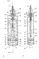
- FIG. 1A is a cross-sectional view of the first embodiment of the ultrasonic probe P of the present disclosure.
- FIG. 1B is a cross-sectional view of the ultrasonic probe P in FIG. 1A and 1B show an example of an ultrasonic probe according to the disclosed technique.
- the element part 1 is a part which converts an electrical signal and an ultrasonic signal.
- the element unit 1 is connected to the element unit substrate 2 and is electrically connected to the electric signal processing circuit 3 through the element unit substrate 2.
- the electric signal processing circuit 3 is electrically connected to a cable 4 and is electrically connected to an ultrasonic diagnostic apparatus main body (not shown) via the cable 4 and a connector (not shown). Thereby, one end of the ultrasonic probe P can be connected to an ultrasonic diagnostic apparatus main body (not shown) via the cable 4 or the like.
- the cable 4 includes a signal line 5 and a cable shield 6 that covers the outer surface of the signal line 5.
- the signal line 5 electrically connects the electrical signal processing circuit 3 and the ultrasonic diagnostic apparatus main body to each other.
- a transmission signal from the ultrasonic diagnostic apparatus main body is transmitted to the element unit 1 via the electric signal processing circuit 3.
- ultrasonic waves are transmitted from the element unit 1 to the subject.
- the transmitted ultrasonic wave is reflected by the subject.
- the element unit 1 converts the ultrasonic wave reflected from the subject into an electric signal.
- the electric signal processing circuit 3 performs signal processing of the electric signal.
- the electrical signal processed by the electrical signal processing circuit 3 is transmitted to the ultrasonic diagnostic apparatus body via the cable 4.
- the element unit 1 includes at least a piezoelectric element.
- the element unit 1 further includes an acoustic matching layer, a backing material 7, an acoustic lens, and the like.
- the element unit 1 of the ultrasonic probe P a part of the energy of the transmission signal from the ultrasonic diagnostic apparatus main body becomes heat, so that the temperature of the element unit 1 rises.
- the electric signal processing circuit 3 is mounted on the circuit unit substrate 8.
- the electrical signal processing circuit 3 includes a transmission drive circuit, a changeover switch, a reception signal amplification circuit, a circuit that delays and adds reception signals, and the like.
- a circuit that performs signal processing of a transmission signal from the ultrasonic diagnostic apparatus body or a circuit that performs signal processing of a reception signal from the element unit 1 is integrated.
- the electric signal processing circuit 3 generates heat in the process of transmitting and receiving signals in these circuits.
- the case 9 houses the element unit 1 and the electric signal processing circuit 3.
- “Accommodating” includes a case where the element unit 1 as an object is partially accommodated as shown in FIGS. 1A and 1B.
- the case 9 is divided into two upper and lower parts (a first part and a second part).
- Each component of the case 9 is bonded with an adhesive or the like so as to cover both the element portion 1 and the electric signal processing circuit 3. That is, the components of the case 9 are joined so as to cover from the element unit 1 to the electric signal processing circuit 3.
- components such as the element unit 1, the element unit substrate 2, and the electric signal processing circuit 3 are accommodated in the case 9.
- the case 9 is preferably made of an insulating and high thermal conductivity material.
- the case 9 is formed, for example, by mixing a filler such as silicon carbide, aluminum nitride, boron nitride, magnesium oxide, aluminum oxide, or aluminum nitride into a resin such as PBT resin, PPS resin, nylon resin, or phenol resin. These materials have a high thermal conductivity of 2 to 15 W / m ⁇ K and an insulating property. By using such a high thermal conductivity material as the material for the case 9, heat can be dispersed throughout the case 9. Thereby, it can suppress that only the specific part of case 9 becomes high temperature.
- the case 9 may be formed with a layer of a material having high thermal conductivity on the inner surface.
- a material having high thermal conductivity As a specific example, graphite may be applied to the inner surface of the case 9 as a highly heat conductive material.
- a layer of a high thermal conductivity material may be formed on the electric signal processing circuit 3 side, and a high thermal conductivity material layer may not be formed on the element portion 1 side.
- the partition portion 10 is integrally formed with one part of the case 9.
- the partition portion 10 formed separately from the case 9 is not limited to this case, and is formed inside the case 9. It may be provided.
- the outer surface of the case 9 is not separated by the partition part 10 and covers from the element part 1 to the electric signal processing circuit 3.
- the partition part 10 is arrange
- a through hole 11 is provided in the partition 10, and the element substrate 2 passes through the through hole 11.
- substrate 2 is comprised by glass or an epoxy resin, for example. It is preferable that the size of the through hole 11 is generally such that the partition portion 10 and the element substrate 2 are in contact with each other. However, the size of the through hole 11 is not limited to this, and heat transfer by air convection through the through hole 11 can be ignored. There may be a gap.
- the through hole 11 may be formed by providing the partition portion 10 in both of the components of the case 9 and providing a notch in the portion of the partition portion 10 through which the element portion substrate 2 passes.
- the partition 10 may be formed integrally with the case 9 by the same material as the case 9.
- the partition part 10 and the case 9 are joined without a gap. Thereby, convection of air can be prevented between the space on the element part 1 side in the case 9 and the space on the electric signal processing circuit 3 side.
- the space on the element portion 1 side in the case 9 separated by the partition portion 10 is filled with hard urethane foam or the like as the heat insulating material 12 (first material 12) having low thermal conductivity.
- the space on the element part 1 side separated by the partition part 10 is a space in the case 9 surrounded by the element part 1 and the partition part 10, and more specifically, the backing material 7 of the element part 1.
- the heat insulating material 12 may be air as long as it has a thermal conductivity lower than that of at least the inner surface of the case 9, and may be air, but the heat insulating material 12 may be a solid material. More preferred.
- thermo conductivity of the heat insulating material 12 on the element unit 1 side is lower than the thermal conductivity of the inner surface of the case 9, heat is generated between the space on the electric signal processing circuit 3 side in the case 9 and the element unit 1. Is difficult to communicate. Thereby, it is possible to suppress the heat generated from the electric signal processing circuit 3 from being transmitted to the element unit 1.
- the heat insulating material 12 may not be filled in the entire space on the element part 1 side separated by the partition part 10, but is filled so as to be in close contact with both the partition part 10 and the element part 1. Is preferred.
- a pre-molded heat insulating material 12 may be installed.
- one part of the case 9 may be provided with a hole 13 communicating with the space between the element part 1 and the partition part 10, and the heat insulating material 12 may be injected from the hole 13. That is, after fitting the upper and lower parts of the case 9, the heat insulating material 12 is injected from the hole 13, and after the heat insulating material 12 is injected, the cover 13 is sealed so as to cover the hole 13.
- the hole 13 is sealed with the lid 14 in a state where the space on the element portion 1 side in the case 9 is filled with the heat insulating material 12. That is, at least the opening on the element part 1 side of the hole 13 is sealed with the heat insulating material 12.
- the lid 14 may be constituted by the heat insulating material 12.
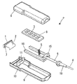
- FIG. 2 is a three-dimensional view of the components of the ultrasonic probe P according to the first embodiment.
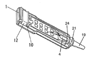
- FIG. 3 shows components and the like inside the ultrasonic probe P in a state where the one side (upper side) of the case 9 is separated in the first embodiment of the ultrasonic probe P.
- each component is housed in the case 9, and after joining the case 9, as shown in FIG. 4, the element portion 1 and the partition portion 10 in the case 9.
- a heat insulating material 12 is injected into a hole 13 provided at a position corresponding to the space between the two. The hole 13 is then sealed with a lid 14.
- the space on the side of the electric signal processing circuit 3 in the case 9 separated by the partition part 10 is a space on the side of the electric signal processing circuit 3 surrounded by the partition part 10 and the case 9, and this space includes a gas such as air. Is filled. That is, gas is in contact with the electric signal processing circuit 3.
- a cable clamp 15 that sandwiches the cable shield 6 that is a part of the cable 4 is disposed inside the case 9.
- the cable clamp 15 is composed of at least two parts, upper and lower.
- the cable clamp 15 sandwiches the cable shield 6 so that the fastening surfaces 16 of the two parts of the cable clamp 15 face each other.
- the screw 17 penetrates both parts of the cable clamp 15, so that the cable clamp 15 is fixed together with the cable 4.
- 1 illustrates a case where the shape of the strain relief 15 is T-shaped when viewed from above, but FIG. 2 illustrates a case where the shape of the strain relief 15 is rectangular when viewed from above.
- At least one arm 18 is connected to the cable clamp 15.
- the arm 18 is also connected to the circuit board 8.
- the arm 18 supports the cable clamp 15 and the circuit board 8.
- the circuit board 8 and the arm 18 are fixed to each other by screws.
- the two arms are connected to the cable clamp 15, but may be one or three or more.
- the arm 18 may be integrally formed with the cable clamp 15 as a part of the cable clamp 15. That is, the cable clamp 15 and the arm 18 may be formed from a series of one member.
- the cable clamp 15 and the arm 18 may be manufactured by integral molding using metal die casting such as aluminum die casting. Thereby, the complicated shape suitable for fixation of the cable 4 and heat dissipation from the electric signal processing circuit 3 can be realized at low cost.
- the cable clamp 15 When the arm 18 is formed integrally with the cable clamp 15 as a part of the cable clamp 15, the cable clamp 15 has a portion (lower portion) following the arm 18 as shown in FIG. Then, the cable shield 6 is sandwiched in the vertical direction at a portion (upper portion) facing the portion. Thereby, the heat of the circuit unit substrate 8 can be efficiently transferred to the cable shield 6 via the arm 18.
- the screw 17 presses the cable clamp 15 so that the cable clamp 15 sandwiches the cable shield 6. You may adhere to. Adhesion in this case may be performed using an adhesive having high thermal conductivity or high conductivity. Further, the cable shield 6 may not be sandwiched by the cable clamp 15. That is, the cable shield 6 may be bonded and fixed to a part of the cable clamp 15 using an adhesive having high thermal conductivity or high conductivity without providing the screw 17 for press-contacting the cable clamp 15.
- the arm 18 is made of a material having a higher thermal conductivity than the heat insulating material 12. By adopting such a material, heat generated on the electric signal processing circuit 3 side can be transferred to the cable shield 6 through the arm 18 while suppressing transfer of heat to the element portion 1.
- the material of the cable clamp 15 and the arm 18 is preferably a metal material such as gold, silver, or copper.
- metal materials aluminum having a low electrical resistivity, a high thermal conductivity, a light weight and a low price is more preferable.
- the ground electrode of the electric signal processing circuit 3 may be disposed at the contact portion with the arm 18 in the circuit unit substrate 8. According to such an arrangement, in addition to fixing the cable 4 by sandwiching the cable shield 6 by the cable clamp 15, the ground electrode of the electric signal processing circuit 3 is electrically connected to the cable shield 6 which is a relatively thick wire. Can be connected. Thereby, the ground impedance of the electric signal processing circuit 3 can be reduced. By reducing the ground impedance, the electric signal processing circuit 3 can reduce the influence of the electromagnetic wave noise from the outside, or can reduce the electromagnetic wave noise emitted to the outside.
- the heat generated in the electric signal processing circuit 3 is transmitted to the cable shield 6 through the wide ground electrode formed on the circuit unit substrate 8 and the arm 18 in direct contact with the ground electrode.
- the emissivity varies greatly depending on the state of the surface of the arm 18.
- the emissivity of a non-oxidized surface having a wavelength of about 1.6 ⁇ m is 0.09, whereas when the surface aluminum is oxidized to form an oxidized surface, the emissivity is 0. 4 (4 times or more).
- the emissivity can be similarly improved by applying a heat radiation paint (heat radiation paint) to the surface of the arm 18.
- the surface of the cable clamp 15 connected to the arm 18 made of aluminum may be oxidized. By subjecting the surface of the cable clamp 15 to oxidation, the heat of the electric signal processing circuit 3 can be efficiently radiated.
- the oxidation treatment may be performed on the entire surface of the arm 18 and the cable clamp 15. Or you may apply an oxidation process or application
- FIG. The surface on the cable clamp 15 side from the center in the longitudinal direction of the arm 18 is subjected to oxidation treatment or heat radiation coating, and the surface on the end side opposite to the cable clamp 15 from the center in the longitudinal direction of the arm 18 is oxidized. It is good also as a structure which does not give a process or application
- the cable clamp 15 and the arm 18 may be formed of a resin mixed with carbon or a metal filler.
- a resin mixed with carbon or a metal filler In this case, a complicated shape suitable for fixing the cable 4 and radiating heat from the electric signal processing circuit 3 can be manufactured at low cost by resin molding.
- carbon carbon black, carbon fiber, graphite, carbon graphite, or the like can be used.
- metal filler fine powders such as silver, copper and nickel, metal oxides such as zinc oxide and tin oxide, or metal fibers of aluminum or stainless steel can be used.
- the resin polyolefin, polyester, phenol, nylon, or the like can be used.
- a conductive resin containing such a carbon or metal filler has a low electrical resistance and a high thermal conductivity as compared with a general resin. Therefore, heat radiation from the electric signal processing circuit 3 and reduction of ground impedance are reduced. It is a suitable material.
- a heat dissipating grease having a higher thermal conductivity than that of the circuit unit substrate 8 may be applied to a portion where the circuit unit substrate 8 and the arm 18 are in contact with each other. Thereby, the heat transfer efficiency from the electric signal processing circuit 3 to the arm 18 can be further improved.
- the heat dissipation grease for example, silicon grease having a thermal conductivity of about 3 W / m ⁇ K can be used.
- the ground impedance of the electric signal processing circuit 3 can be reduced, so that electromagnetic wave noise and radiation noise from the outside can be reduced. Can do.
- carbon or a metal filler may be mixed.
- metal filler fine powder such as silver, copper or nickel, metal oxide such as zinc oxide or tin oxide, or metal fiber of aluminum or stainless steel can be used.
- metal oxide such as zinc oxide or tin oxide
- carbon carbon black, carbon fiber, graphite, carbon graphite, or the like can be used.
- a strain relief 19 that penetrates the cable 4 is provided at a location where the case 9 and the cable 4 are connected. Specifically, a strain relief 19 that penetrates the cable 4 outside the case 9 and contacts the case 9 is provided. The strain relief 19 is provided to prevent disconnection due to a sharp bend of the cable 4.
- the cable clamp 15 is connected to a heat radiating plate 24 in the case described later, and the heat radiating plate 24 in the case is further connected to a screw portion 20 extending toward the outside of the case 9.
- a radiation plate 21 (second heat radiating plate 21) is screwed into the screw portion 20.
- the heat radiating plate 21 is one or more disc-shaped plates that are insert-molded in the strain relief 19 and is made of a metal such as aluminum.
- a screw hole that is screwed into the screw portion 20 is formed at the center of the heat radiating plate 21.
- the heat radiating plate 21 has three disc shapes. According to such a structure, the screw part 20 and the heat sink 21 are connected by rotating the heat sink 21 together with the strain relief 19 and screwing it into the screw part 20.
- a high heat conductive grease or a high heat conductive adhesive may be applied to the connecting portion by the screw.
- the method is not limited to such a method using screws, and the cable clamp 15 and the heat radiating plate 21 may be connected using other methods.
- the cable clamp 15, the heat sink 24 in the case, and the screw part 20 may be integrally formed.
- the part in which the cable clamp 15, the heat dissipation plate 24 in the case, and the screw portion 20 are integrally formed is composed of two parts, upper and lower, to sandwich the cable 4, and these two parts are fixed with screws 17.
- Such a configuration in which the components are integrally formed is preferable because the heat conduction efficiency is improved as compared with the case where the components are formed separately and then connected.
- the cross-sectional area of the strain relief 19 that covers the heat sink 21 gradually decreases in the axial direction of the cable 4 from the connecting portion (contact portion) with the cable clamp 15 toward the ultrasonic diagnostic apparatus main body.
- Such a shape of the strain relief 19 prevents the cable 4 from being sharply bent. Thereby, disconnection of the signal line 5 of the cable 4 and the cable shield 6 can be prevented.
- the periphery of the heat sink 21 made of a metal such as aluminum may be covered with a strain relief 19 made of a non-conductive elastomer having a high thermal conductivity. Thereby, the electrical insulation of the ultrasonic probe P is ensured.
- the emissivity of the elastomer is about 0.95, which is much higher than the emissivity of metals such as aluminum. Therefore, by covering the heat sink 21 with the strain relief 19 made of elastomer, more efficient heat dissipation can be achieved. Can be realized.
- the arm 18 and the cable clamp 15 may be manufactured as separate parts, but this is not a limitation.
- the arm 18 and the cable clamp 15 may be divided. According to such a method, the screw portion 20 can be processed before the arm 18 and the cable clamp 15 are divided.
- the cable 4 sandwiched between the cable clamps 15 can be firmly fixed by screwing the strain relief 19 with the heat sink 21 inserted into the screw portion 20.
- a groove 23 extending in a direction perpendicular to the direction in which the cable clamp 15 sandwiches the cable 4 (the axial direction of the cable 4) may be formed in the screw portion 20.
- the screw portion 20 is divided into a plurality of regions (for example, three divisions or four divisions).
- the strain relief 19 when the strain relief 19 is screwed into the screw portion 20, the cable 4 can be tightened from a plurality of directions (for example, three directions or four directions), so that the cable 4 can be fixed more firmly.
- the tip of the threaded portion 20 is thin and tapered, it is advantageous when the strain relief 19 is screwed into the threaded portion 20 and the cable 4 is tightened.
- the in-case heat radiation plate 24 (first heat radiation plate 24) may be formed so as to be sandwiched between the two components of the case 9 at the joint portion of the case 9 components.
- the in-case heat sink 24 is in contact with the cable clamp 15 and the heat sink 21.
- the in-case heat radiating plate 24 is made of, for example, a metal material such as aluminum. Furthermore, you may arrange
- the heat sink 24 in the case and the heat sink 21 constitute a heat sink that surrounds the cable 4 and is connected to the cable clamp 15.
- the heat of the cable clamp 15 can be more transferred to the heat radiating plate 21 via the in-case heat radiating plate 24, so that the heat generated in the electric signal processing circuit 3 compared to the case without the in-case heat radiating plate 24.
- the heat transfer efficiency to the heat sink 21 can be increased. As a result, the efficiency of heat radiation to the outside via the heat sink 21 on the strain relief 19 side can be improved.
- the recess 22 formed in the case 9 and the recess 22 formed in the strain relief 19 are positioned so as to face each other.
- the recess 22 functions as a space for storing the adhesive.
- excess adhesive is stored in the recess 22.
- grease or adhesive having higher thermal conductivity than the cable clamp 15 may be applied to the contact surface of the cable clamp 15 with the cable 4.
- the heat transfer efficiency from the cable clamp 15 to the cable shield 6 is improved, and the cable 4 can be more reliably fixed with the adhesive.
- the grease having high thermal conductivity for example, silicon grease having a thermal conductivity of about 3 W / m ⁇ K can be used.
- it is preferable that such grease or adhesive has conductivity.
- carbon or a metal filler may be mixed.
- the metal filler include fine powders such as silver, copper, and nickel, metal oxides such as zinc oxide and tin oxide, and metal fibers of aluminum or stainless steel.
- Examples of carbon include carbon black, carbon fiber, graphite, and carbon graphite.
- FIG. 5 is an exploded view of the ultrasonic probe X used in the simulation.
- the ultrasonic probe X includes an element unit 1, an element unit substrate 2, an electric signal processing circuit 3, a signal line 5, a cable shield 6, a backing material 7, a circuit unit substrate 8, and a case 9.
- the cable clamp 15 and the strain relief 19 are provided.
- the ultrasonic probe X shown in FIG. 5 is common to the ultrasonic probe P shown in FIG. Although the structure of the electric signal processing circuit 3 and the shape of the cable clamp 15 are different, the basic configuration is almost common, and the ultrasonic probe X shown in FIG. For simplicity, the electromagnetic shielding member is omitted.
- the element unit 1 is electrically connected to the electric signal processing circuit 3 via the element unit substrate 2.
- the electric signal processing circuit 3 is electrically connected to the ultrasonic diagnostic apparatus main body via the signal line 5.
- FIG. 5 shows a state before the two components of the case 9 are joined. However, in the simulation, the element unit 1, the electric signal processing circuit 3, the cable shield 6, the cable clamp 15 and the like are included. Two parts of the case 9 are joined to each other.
- FIG. 6A shows a simulation result when the element portion 1 of the ultrasonic probe X1 is held upward with respect to the ground.
- FIG. 6B shows a simulation result when the element portion 1 of the ultrasonic probe X1 is held downward with respect to the ground.
- the ultrasound probe X1 is oriented in any orientation.
- the ultrasonic probe X1 when not in use is stored in a probe holder (not shown) of the ultrasonic diagnostic apparatus main body with the element unit 1 facing upward, for example.
- the temperature of the element unit 1 rises. Since the temperature of the element unit 1 is restricted, when the temperature of the element unit 1 rises, the voltage that can be applied to the element unit 1 is limited. As a result, the output of the transmission voltage to the ultrasound probe X1 cannot be increased to a necessary ultrasound output value, and the sensitivity of the ultrasound diagnostic apparatus is reduced. From the simulation results, the present inventors have found that the propagation of heat due to the convection of air in the case 9 leads to a serious temperature rise of the element unit 1 particularly when the element unit 1 is held upward. .
- FIG. 7A shows a simulation result (result shown in FIG. 6A) when air is filled in the entire space in the case 9 as a comparison target.
- FIG. 7B shows a simulation result when the entire space in the case 9 is filled with a heat insulating material other than air, specifically, a hard urethane foam.
- the maximum surface temperature of the element unit 1 is 44.8 ° C.
- the front of the case 9 (the electric signal processing circuit 3 is disposed).
- the maximum surface temperature of the side surface) is 42.4 ° C.
- the maximum surface temperature of the side surface of the case 9 is 45.8 ° C.
- FIG. 7B when the space inside the case 9 is filled with a heat insulating material other than air, the maximum surface temperature of the element portion 1 is 50.9 ° C., and the maximum surface temperature of the front surface of the case 9 is 45.
- the maximum surface temperature of the side surface of the case 9 is 49.3 ° C.
- the surface of the element portion 1 and the case 9 when the entire space in the case 9 is filled with a heat insulating material other than air is more than when the entire space in the case 9 is filled with air. It turns out that temperature becomes high. Thus, even if the entire interior of the case 9 is filled with a heat insulating material other than air, there is no effect of reducing the surface temperature of the element portion 1 and the case 9 of the electric signal processing circuit 3, and the surface temperature of a specific part increases. You can see that
- the heat generation state of the ultrasonic probe X3 provided with the partition portion 10 that partitions the space in the case 9 will be described with reference to FIG.
- the partition portion that is disposed between the element portion 1 and the electric signal processing circuit 3 so as to spatially separate the element portion 1 and the electric signal processing circuit 3 and contact the case 9 10 is provided.
- the space on the element part 1 side is filled with a heat insulating material other than air, specifically, hard urethane foam, and the space on the electric signal processing circuit 3 side is filled with air. Filled.
- FIG. 8 shows the state in which the element unit 1 is held upward with respect to the ground in the ultrasonic probe X3, no power is applied to the element unit 1, and the power consumption of the electric signal processing circuit 3 is 3W.
- the simulation result which calculated the surface temperature of each site
- the maximum surface temperature of the element part 1 is 35.7 degreeC. This is lower than the temperature (44.8 ° C.) when all the spaces in the case 9 described with reference to FIG. 7A are filled with air.
- the maximum surface temperature of the front surface of the case 9 is 44.8 ° C.
- the maximum surface temperature of the side surface of the case 9 is 45.2 ° C.
- FIG. 9 shows the state in which the element unit 1 is held upward with respect to the ground in the ultrasonic probe X4, no power is applied to the element unit 1, and the power consumption of the electric signal processing circuit 3 is 3W. It is the simulation result which calculated the surface temperature of each part in the case of. As shown in FIG. 9, the maximum surface temperature of the element unit 1 is 35.7 ° C., the maximum surface temperature of the front surface of the case 9 is 44.0 ° C., and the maximum surface temperature of the side surface of the case 9 is 43.5 ° C. The maximum surface temperature (35.7 ° C.) of the element portion 1 in FIG. 9 is lower than the temperature (44.8 ° C.) described with reference to FIG.
- the maximum surface temperature (44.0 ° C.) in front of the case 9 in FIG. 9 is also lower than the temperature (44.8 ° C.) when the arm 18 described with reference to FIG. 8 is not provided.
- the heat generated from the electric signal processing circuit 3 is efficiently transferred to the strain relief 19 through the arm 18 and the cable clamp 15 by connecting the circuit board 8 to the arm 18. Can be heated. Thereby, not only the surface temperature of the element unit 1 but also the surface temperature of the front surface of the case 9 can be lowered.
- FIG. 10A shows a simulation result (result shown in FIG. 6A) when a modified PPE resin is used as the material of the case 9 as a comparison target.
- FIG. 10B shows a simulation result when a non-conductive high thermal conductivity PBT in which a boron nitride filler is mixed into the PBT resin is used as the material of the case 9. As shown in FIG.
- FIG. 11 shows the state in which the element unit 1 is held upward with respect to the ground in the ultrasonic probe X6, power is not applied to the element unit 1, and the power consumption of the electric signal processing circuit 3 is 3W. It is the simulation result which calculated the surface temperature of each part in the case of. As shown in FIG.
- the maximum surface temperature of the element portion 1 is 35.5 ° C.
- the maximum surface temperature of the front surface of the case 9 is 41.8 ° C.
- the maximum surface temperature of the side surface of the case 9 is 44.2 ° C. Therefore, compared with the case of the ultrasonic probe X1 shown in FIGS. 6 (a) and 6 (b), even when the element unit 1 is held upward with respect to the ground, the element unit 1 It can be seen that the surface temperature of both the case 9 and the case 9 can be lowered.
- the heat insulating material 12 and the case 9 are brought into contact with each other.
- the partition 10 thus formed separates the space in the case 9 into a space on the element portion 1 side and a space on the electric signal processing circuit 3 side. Thereby, air convection between the space on the element part 1 side and the space on the electric signal processing circuit 3 side in the case 9 can be eliminated, and heat transfer from the electric signal processing circuit 3 to the element part 1 can be suppressed. .
- a heat insulating layer (heat insulating material 12) is formed between the partition portion 10 and the element portion 1 in the case, or a heat insulating medium (heat insulating material 12) is filled.
- the heat generated in the electric signal processing circuit 3 is efficiently transmitted to the cable 4 and the strain relief 19 via the arm 18 that supports the cable clamp 15.
- the heat generated in the electric signal processing circuit 3 is transferred to the portion of the case 9 that covers the electric signal processing circuit 3 by air convection in the space on the electric signal processing circuit 3 side in the case 9. . Thereby, the heat of the electric signal processing circuit 3 can be radiated.
- the ultrasonic probes X3, X4, and X6 (and the ultrasonic probe P) that can be connected to the ultrasonic diagnostic apparatus main body include an element unit 1 that converts electrical signals and ultrasonic waves to each other, and an element unit. 1, an electrical signal processing circuit 3 electrically connected to 1, a case 9 that houses the element unit 1 and the electrical signal processing circuit 3, and an element unit substrate that electrically connects the element unit 1 and the electrical signal processing circuit 3. 2 and a partition portion 10 that is arranged in contact with the case 9 and separates the element portion 1 and the electric signal processing circuit 3, and is a space on the element portion 1 side in the case 9 and separated by the partition portion 10.
- a first material (heat insulating material 12) having a thermal conductivity lower than that of the substance forming the inner wall surface of the case 9 is filled. Thereby, the heat generated from the electric signal processing circuit 3 as a heat source can be efficiently radiated and heat transfer to the element unit 1 can be suppressed. If it has at least these structures, the objective of this indication technique mentioned above can be achieved.
- the first embodiment it is possible to suppress heat generated in the electric signal processing circuit 3 and the like from being transferred to the element unit 1 by air convection, particularly in a state where the element unit 1 is held upward. Thereby, since the temperature rise of the element part 1 can be reduced, the sensitivity fall of the ultrasonic probe by the restriction
- FIG. 12A is a cross-sectional view of the ultrasonic probe Q according to the first modification of the first embodiment.
- FIG. 12B is a cross-sectional view of the ultrasonic probe Q taken along the line AA ′ in FIG.
- the same reference numerals are used for the same configuration of the ultrasonic probe as described in the first embodiment, and detailed description thereof is omitted.
- a partition plate 25 made of a plurality of flat plates is formed as the partition portion 10 so as to be in contact with the case 9 with a predetermined interval.
- the space between the plurality of partition plates 25 and the space between the partition plates 25 and the element unit 1 are filled with air, respectively.
- one part of the case 9 divided into two parts, upper and lower, is provided with a continuous partition part composed of a plurality of partition plates 25 that spatially separate the element part 1 and the electric signal processing circuit 3.
- the partition plate 25 is formed integrally with one part of the case 9, but it may be arranged inside the case 9 after the partition plate 25 is formed individually.
- the outer surface of the case 9 is not separated by the partition plate 25 and covers from the element portion 1 to the electric signal processing circuit 3.
- the partition plate 25 is disposed so as to be in contact with the case 9, and the element part substrate 2 passes therethrough.
- the element part substrate 2 passes through the through holes 11 provided in the respective partition plates 25.
- the size of the through hole 11 is preferably such that the partition plate 25 and the element part substrate 2 are in contact with each other.
- the partition plate 25 is not formed on one part of the case 9, but the partition plate 25 may be provided on both sides of the upper and lower parts of the case 9.
- the through holes 11 through which the element substrate 2 penetrates may be formed by providing notches in the upper and lower partition plates 25.
- the partition plate 25 may be formed integrally with the case 9 using the same material as the case 9. By forming the partition plate 25 integrally with the case 9, the partition plate 25 and the case 9 are joined without a gap. Thereby, the convection of the air between the space by the side of the element part 1 in the case 9 and the space by the side of the electric signal processing circuit 3 can be prevented.
- partition plates 25 are formed, but at least two partition plates 25 may be provided.
- the space in the case 9 is partitioned by the partition plate 25 and an air layer is provided in each of the partitioned spaces, so that the electrical signal processing can be performed without arranging a heat insulating material other than air in the case 9. Heat transfer from the circuit 3 to the element unit 1 can be prevented.
- FIG. 13A is a cross-sectional view of an ultrasonic probe R according to Modification 2 of the first embodiment.
- FIG. 13B is a cross-sectional view of the ultrasonic probe R taken along the line AA ′ in FIG.
- the same reference numerals are used for the same configuration of the ultrasonic probe as described in the first embodiment, and detailed description thereof is omitted.
- a partition plate 26 composed of two flat plates arranged so as to be in contact with the case 9 with a predetermined interval is used as the partition portion 10. Further, a heat insulating material 27 other than air is filled between the two partition plates 26 so as to contact the facing surface of the partition plate 26 and the case 9. In addition, the space between the element portion 1 and the partition plate 26 is filled with a high thermal conductive material 28 having a thermal conductivity higher than that of the heat insulating material 27. That is, the space on the element portion 1 side in the case 9 partitioned by the partition plate 26 is filled with the heat insulating material 27 and the high heat conductive material 28.
- partition plates 26 for spatially separating the element portion 1 and the electric signal processing circuit 3 are provided in one part of the case 9 divided into two parts, upper and lower.
- the partition plate 26 is formed integrally with one part of the case 9, but it may be arranged inside the case 9 after the partition plate 26 is individually formed.
- the outer surface of the case 9 is not separated by the partition plate 26 and covers from the element portion 1 to the electric signal processing circuit 3.
- the partition plate 26 is disposed so as to be in contact with the case 9, and the element substrate 2 passes therethrough.
- the element part substrate 2 passes through each through hole 11 provided in the partition plate 26.
- the size of the through hole 11 is preferably such that the partition plate 26 and the element part substrate 2 are in contact with each other.
- the partition plate 26 is not formed on one part of the case 9, but the partition plate 26 may be provided on both sides of the upper and lower two parts of the case 9.
- the through holes 11 through which the element substrate 2 penetrates may be formed by providing notches in the upper and lower partition plates 26.
- the partition plate 26 may be formed integrally with the case 9 using the same material as the case 9. By forming the partition plate 26 integrally with the case 9, the partition plate 26 and the case 9 are joined without a gap. Thereby, the convection of the air between the space by the side of the element part 1 in the case 9 and the space by the side of the electric signal processing circuit 3 can be prevented.
- the heat insulating material 27 may be, for example, hard urethane foam, expanded polystyrene foam, glass wool, rock wool, air, wood, or the like.
- the high thermal conductive material 28 is a material in which a filler such as silicon carbide, aluminum nitride, boron nitride, magnesium oxide, aluminum oxide, or aluminum nitride is mixed in a resin such as PBT resin, PPS resin, nylon resin, or phenol resin. Also good.
- each component of the ultrasonic probe R is housed in the case 9, and after the case 9 is joined, the heat insulating material is inserted from the hole provided in the case 9.
- 27 and high heat conductive material 28 may be injected and sealed with a lid.
- the hole of the case 9 communicates with a space in the case 9 where the heat insulating material 27 and the high thermal conductive material 28 are disposed.
- the heat insulating material 27 is disposed between the partition plates 26, and the high heat conductive material 28 is disposed in the space between the element unit 1 and the partition plate 26. According to such an arrangement, the heat insulating material 27 suppresses heat generated in the electric signal processing circuit 3 from being transferred to the element unit 1. In addition, the heat generated in the element unit 1 can be dissipated by being transmitted to the case 9 through the high thermal conductive material 28. As a result, an increase in the surface temperature of the element unit 1 can be reduced, so that a decrease in sensitivity of the ultrasonic probe R due to the limitation of the ultrasonic output related to the regulation of the surface temperature of the element unit 1 can be reduced. .
- FIG. 14A is a cross-sectional view of the second embodiment of the ultrasonic probe according to the present disclosure.
- FIG. 14B is a cross-sectional view of the ultrasonic probe S taken along the line AA ′ in FIG.
- the same reference numerals are used for the same configuration of the ultrasonic probe as described in the first embodiment, and detailed description thereof is omitted.
- One end of the ultrasonic probe S can be connected to an ultrasonic diagnostic apparatus main body (shown) via the cable 4.
- the difference between the second embodiment and the first embodiment is the structure of the case 9. Specifically, in the first embodiment, the case 9 is divided into two upper and lower parts, whereas in the second embodiment, the element part case 29 (first part 29) for housing the element part 1 is used. ) And a circuit unit case 30 (second component 30) for housing the electric signal processing circuit 3.
- the element part case 29 covering the element part 1 and the circuit part case 30 covering the electric signal processing circuit 3 are joined with an adhesive or the like, whereby the element part 1, the element part substrate 2, the electric signal processing in the case 9. Components such as the circuit 3 are accommodated. In this way, the element unit 1 and the electric signal processing circuit 3 are accommodated in the case 9.
- the case 9 is preferably formed of a material having insulating properties and high thermal conductivity (insulating high thermal conductivity material).
- insulating high thermal conductivity material examples include a material such as PBT resin, PPS resin, nylon resin, and phenol resin mixed with a filler such as silicon carbide, aluminum nitride, boron nitride, magnesium oxide, aluminum oxide, and aluminum nitride. is there. These materials have a high thermal conductivity of 2 to 15 W / m ⁇ K and have insulating properties.
- the case 9 may be formed with a layer of a material having high thermal conductivity on the inner surface.
- graphite may be applied to the inner surface of the case 9 as a highly heat conductive material.
- a configuration may be adopted in which a layer of a high thermal conductivity material is formed on the inner surface of the circuit unit case 30 and a layer of a high thermal conductivity material is not formed on the inner surface of the element unit case 29. Such a configuration is desirable because the heat dissipated from the electric signal processing circuit unit 3 is dispersed and the heat distribution to the element unit 1 side can be suppressed.
- An element case lid 31 that spatially separates the element unit 1 and the electric signal processing circuit 3 is provided between the element unit 1 and the electric signal processing circuit 3 in the case 9.
- the element case lid 31 corresponds to the partition portion 10 in the first embodiment.
- the element case lid 31 is disposed so as to be in contact with the case 9, and the element part substrate 2 passes therethrough.
- the element part substrate 2 passes through the through hole 11 provided in the element case lid 31.
- the size of the through hole 11 is preferably such that the element case lid 31 and the element part substrate 2 are in contact with each other.
- the element case cover 31 covers the opening of the element part case 29 (the opening of the element part case 29 on the electric signal processing circuit 3 side).
- the element case lid 31 is formed on a plane including the joint surface between the element case 29 and the circuit case 30. That is, the element part case 29 and the circuit part case 30 are joined to each other at a position in contact with the element case cover 31.
- the element case lid 31 may be formed of, for example, a modified PPE resin.
- the element case lid 31 may be formed of the same material as the case 9.
- the space on the element part 1 side separated by the element case lid 31 is filled with hard urethane foam or the like as the heat insulating material 12 (first material 12) having low thermal conductivity.
- the space on the element portion 1 side separated by the element case lid 31 is a space in the case 9 surrounded by the element portion 1, the element case lid 31, and the element portion case 29, and more specifically, the element portion 1. This is a space in the case 9 surrounded by the backing material 7 of the part 1, the element case lid 31 and the element part case 29.
- the thermal conductivity of the heat insulating material 12 may be air as long as it has a lower thermal conductivity than the thermal conductivity of at least the inner surface of the element case 29, and may be air, but the heat insulating material 12 Is more preferably a solid material.
- thermo conductivity of the heat insulating material 12 on the element part 1 side is lower than the thermal conductivity of the inner surface of the element part case 29, the space on the electric signal processing circuit 3 side in the case 9 and the element part 1 It becomes difficult to transmit heat. Thereby, it is possible to suppress the heat generated from the electric signal processing circuit 3 from being transmitted to the element unit 1.
- the heat insulating material 12 may fill the gap between the element case lid 31 and the element part substrate 2.
- the heat insulating material 12 is preferably filled so as to be in close contact with both the element case lid 31 and the element portion 1.
- the element case cover 31 and the element part case 29 the pre-molded heat insulating material 12 is installed in the element part case 29, and then the element case cover 31 may cover the opening of the element case 29.
- the hole 13 may be provided in the element case lid 31 and the heat insulating material 12 may be injected from the hole 13. That is, after covering the opening of the element part case 29 with the element case cover 31, the heat insulating material 12 is injected from the hole 13, and after the heat insulating material 12 is injected, the hole 14 is sealed with the cover 14.
- the heat insulating material 12 can be reliably filled in the space surrounded by the element part 1, the element case lid 31, and the element part case 29 without a gap.
- the hole 13 is sealed with the lid 14 in a state where the space on the element portion 1 side in the case 9 is filled with the heat insulating material 12. That is, at least the opening on the element part 1 side of the hole 13 is sealed with the heat insulating material 12.
- FIG. 15 three-dimensionally shows a state where the element unit case 29 and the circuit unit case 30 are separated from each other in the ultrasonic probe S according to the second embodiment.
- FIG. 16 shows a state in which the heat insulating material 12 is injected from the hole 13.
- the heat insulating material is provided in the hole 13 of the element case lid 31 provided in advance. 12 is injected. After injecting the heat insulating material 12, the hole 13 is sealed with a lid 14. Then, the element part board
- the space on the electric signal processing circuit 3 side surrounded by the element case lid 31 and the circuit unit case 30 is filled with a gas such as air. That is, gas is in contact with the electric signal processing circuit 3.
- the circuit unit case 30 has a box shape opened to the element unit 1 side, but the shape of the circuit unit case 30 is not limited thereto.
- the circuit unit case 30 may be composed of two upper and lower parts, and the electric signal processing circuit 3 may be sandwiched from above and below by these parts.
- the in-case heat radiation plate 24 sandwiched between the two components of the circuit unit case 30 can be easily arranged. The heat generated from the signal processing circuit 3 can be radiated more efficiently.
- the ultrasound probe S according to the second embodiment of the present disclosure technique is configured so that the element portion 1 and the electric signal processing are performed by the element case lid 31 formed so as to be in contact with the heat insulating material 12 and the case 9.
- the circuit 3 is spatially separated. As a result, air convection between the space on the element unit 1 side and the space on the electric signal processing circuit 3 side in the case 9 can be eliminated, and heat transfer from the electric signal processing circuit 3 to the element unit 1 can be prevented. Can be suppressed.
- the heat generated in the electric signal processing circuit 3 is efficiently transferred to the cable 4 and the strain relief 19 via the arm 18 that supports the cable clamp 15.
- the ultrasonic probe S that can be connected to the ultrasonic diagnostic apparatus body includes an element unit 1 that mutually converts an electric signal and an ultrasonic wave, and an electric signal processing circuit 3 that is electrically connected to the element unit 1.
- a case 9 that houses the element unit 1 and the electric signal processing circuit 3, an element unit substrate 2 that electrically connects the element unit 1 and the electric signal processing circuit 3, and a case 9.
- the first material (the heat insulating material 12) having a thermal conductivity lower than the thermal conductivity is filled. Thereby, the heat generated from the electric signal processing circuit 3 as a heat source can be efficiently radiated and heat transfer to the element unit 1 can be suppressed. If it has at least these structures, the objective of this indication technique mentioned above can be achieved.
- the second embodiment it is possible to suppress heat generated in the electric signal processing circuit 3 or the like from being transferred to the element unit 1 by air convection, particularly in a state where the element unit 1 is held upward.
- the temperature rise of the element part 1 can be reduced, the sensitivity fall of the ultrasonic probe by the restriction
- FIG. 17A is a cross-sectional view of an ultrasonic probe T according to Modification 1 of the second embodiment.
- FIG. 17B is a cross-sectional view of the ultrasonic probe T taken along the line AA ′ in FIG.
- the same reference numerals are used for the same ultrasonic probe configurations as those described in the first embodiment and the second embodiment, and detailed description thereof is omitted.
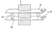
- three partition plates 32 are further provided on the element portion 1 side of the element case cover 31 with respect to the element case cover 31 and at a predetermined interval from each other. It has been.
- the respective partition plates 32 and the element case lid 31 are connected to each other by being penetrated by the connecting portion 34.
- Each partition plate 32 is disposed so as to be in contact with the element portion case 29, similarly to the element case lid 31.
- the space between the partition plates 32, the space between the partition plate 32 and the element case lid 31, and the space between the partition plate 32 and the element portion 1 are filled with air to form an air layer. Yes.
- an element case lid 31 that spatially separates the element unit 1 and the electric signal processing circuit 3 is provided between the element unit 1 and the electric signal processing circuit 3 in the case 9.
- Three partition plates 32 made of flat plates arranged at predetermined intervals from each other are further provided on the element portion 1 side of the element case lid 31.
- Each partition plate 32 and element case lid 31 are connected by a connecting portion 34.
- Each partition plate 32 is disposed in contact with the element portion case 29, and the element portion substrate 2 passes through each partition plate 32 and the element case lid 31.
- the element part substrate 2 passes through the through holes 11 provided in the vicinity of the center of each element case lid 31 and the partition plate 32.
- the size of the through hole 11 is preferably such that each partition plate 32 and the element case lid 31 are in contact with the element part substrate 2, but not limited to this, air convection through the through hole 11. There may be a gap that allows negligible heat transfer. Furthermore, the through hole 11 through which the element part substrate 2 passes may be sealed with an adhesive or the like.
- partition plates 32 are formed, but at least one partition plate 32 is sufficient.
- the partition plate 32 may be formed of the same material as that of the element case lid 31, or may be formed of the same material as that of the element portion case 29.
- the space in the case 9 is partitioned by the element case lid 31 and the partition plate 32, and an air layer is provided in each of the partitioned spaces. Thereby, it is possible to prevent heat transfer from the electric signal processing circuit 3 to the element unit 1 without arranging a heat insulating material other than air in the case 9.
- FIG. 18A is a cross-sectional view of an ultrasonic probe U according to Modification 2 of the second embodiment.
- FIG. 18B is a cross-sectional view of the ultrasonic probe U taken along the line AA ′ in FIG.
- the same reference numerals are used for the same ultrasonic probe configurations as those described in the first embodiment and the second embodiment, and detailed description thereof is omitted.
- a single partition plate 33 made of a flat plate arranged at a predetermined interval with respect to the element case lid 31 is further provided on the element portion 1 side than the element case lid 31.
- the partition plate 33 and the element case lid 31 are connected to each other by being penetrated by the connecting portion 34.
- the partition plate 33 is disposed so as to contact the element case 29.
- a heat insulating material 27 is disposed between the partition plate 33 and the element case lid 31.
- the heat insulating material 27 is disposed so as to contact the opposing partition plate 33 and the surface of the element case lid 31 and the element portion case 29.
- a high thermal conductive material 28 having a higher thermal conductivity than the thermal conductivity of the heat insulating material 27 is disposed.
- the element substrate 2 penetrates the element case lid 31 and the partition plate 33.
- the element part substrate 2 passes through the through hole 11 provided near the center of the partition plate 33 and the element case lid 31.
- the size of the through hole 11 is preferably such that the element case lid 31 and the partition plate 33 are in contact with the element part substrate 2.
- the partition plate 33 may be formed of the same material as that of the element case lid 31, or may be formed of the same material as that of the element portion case 29.
- the connecting portion 34 when the element case lid 31 and the partition plate 33 are connected by the connecting portion 34, when the element case lid 31 covers the opening of the element case 29, the partition plate 33 connected to the element case lid 31 is also simultaneously connected to the element case. 29 can be stored at a constant interval.
- the heat insulating material 27 may be, for example, hard urethane foam, expanded polystyrene foam, glass wool, rock wool, air, wood, or the like.
- the high thermal conductive material 28 is a material in which a filler such as silicon carbide, aluminum nitride, boron nitride, magnesium oxide, aluminum oxide, or aluminum nitride is mixed in a resin such as PBT resin, PPS resin, nylon resin, or phenol resin. Also good.
- the heat insulating material 27 and the high heat conductive material 28 are arranged in this order. Also good.
- the heat insulating material 27 and the high thermal conductive material 28 may be arranged in the element portion case 29 using the holes 13 provided in the partition plate 33 and the element case lid 31. Specifically, after the element unit 1 is accommodated in the element unit case 29 and the partition plate 33 and the element case lid 31 are arranged so as to cover the opening of the element unit case 29, as shown in FIG.
- the high thermal conductivity material 28 is injected into the space between the element unit 1 and the partition plate 33.
- the injected high thermal conductive material 28 is cooled and solidified.
- the heat insulating material 27 is injected into the space between the partition plate 33 and the element case lid 31 from the hole 13.
- the heat insulating material 27 may be, for example, hard urethane foam, expanded polystyrene foam, glass wool, rock wool, air, wood, or the like.
- the high thermal conductive material 28 is a material in which a filler such as silicon carbide, aluminum nitride, boron nitride, magnesium oxide, aluminum oxide, or aluminum nitride is mixed in a resin such as PBT resin, PPS resin, nylon resin, or phenol resin. Also good.
- the heat insulating material 27 is disposed between the element case lid 31 and the partition plate 33, and the high heat conductive material 28 is disposed between the element portion 1 and the partition plate 33. According to such an arrangement, the heat insulating material 27 can suppress the heat generated in the electric signal processing circuit 3 from being transferred to the element unit 1. Furthermore, since the heat generated in the element portion 1 is transmitted to the element portion case 29 via the high heat conductive material 28 by the high heat conductive material 28, heat can be dissipated. As a result, an increase in the surface temperature of the element unit 1 can be reduced, so that a decrease in sensitivity of the ultrasonic probe due to the limitation of the ultrasonic output related to the regulation of the surface temperature of the element unit 1 can be reduced.
- FIG. 21A is a cross-sectional view of an ultrasonic probe V according to Modification 3 of the second embodiment.
- FIG. 21B is a cross-sectional view of the ultrasonic probe V taken along the line AA ′ in FIG.
- the same reference numerals are used for the same ultrasonic probe configurations as those described in the first embodiment and the second embodiment, and detailed description thereof is omitted.
- the element case lid 31 is sandwiched between the element case 29 and the circuit case 30. That is, the element case lid 31 is formed on a plane including the joint surface between the element case 29 and the circuit case 30. Thereby, the element part case 29 and the circuit part case 30 are connected via the element case cover 31 so as not to be in direct contact. That is, the element case lid 31 extends to the joint between the element case 29 and the circuit case 30.
- the element case lid 31 is formed of a material (for example, modified PPE resin) having a thermal conductivity lower than that of the element case 29 and the circuit case 30.
- the element case lid 31 having a low thermal conductivity is interposed between the element part case 29 and the circuit part case 30 formed of a material having a high thermal conductivity. 29 and circuit part case 30 do not contact directly. Therefore, heat transfer between the element unit case 29 and the circuit unit case 30 can be suppressed.
- the temperature rise of the circuit unit case 30 becomes larger than the temperature increase of the element unit case 29.
- the heat transfer from the circuit unit case 30 to the device unit case 29 can be suppressed by providing the device case lid 31, an increase in the surface temperature of the device unit 1 can be reduced. Accordingly, it is possible to reduce a decrease in sensitivity of the ultrasonic probe due to the limitation of the ultrasonic output related to the regulation of the surface temperature of the element unit 1.
- Modification 3 of the second embodiment can be appropriately combined with Modification 1 or Modification 2 of the second embodiment. That is, for example, the partition plate 32 (Modification 1) and the partition plate 33 (Modification 2) are arranged in contact with the inner wall of the element case 29, and the element case lid 31 is placed in the element as in Modification 3.
- the element case 29 and the circuit unit case 30 may be joined so as to be sandwiched between the unit case 29 and the circuit unit case 30.
- the disclosed technique prevents convection of air between the element unit 1 and a circuit unit (electric signal processing circuit 3) that is a heat source in the case of the ultrasonic probe, and efficiently uses heat from the circuit unit. Since it can dissipate heat well, it is particularly suitable for an ultrasonic probe having a circuit part as a heat generation source in a case.
Landscapes
- Health & Medical Sciences (AREA)
- Life Sciences & Earth Sciences (AREA)
- Pathology (AREA)
- General Health & Medical Sciences (AREA)
- Physics & Mathematics (AREA)
- Surgery (AREA)
- Biophysics (AREA)
- Engineering & Computer Science (AREA)
- Biomedical Technology (AREA)
- Heart & Thoracic Surgery (AREA)
- Medical Informatics (AREA)
- Molecular Biology (AREA)
- Nuclear Medicine, Radiotherapy & Molecular Imaging (AREA)
- Animal Behavior & Ethology (AREA)
- Radiology & Medical Imaging (AREA)
- Public Health (AREA)
- Veterinary Medicine (AREA)
- Gynecology & Obstetrics (AREA)
- Chemical & Material Sciences (AREA)
- Analytical Chemistry (AREA)
- Biochemistry (AREA)
- General Physics & Mathematics (AREA)
- Immunology (AREA)
- Ultra Sonic Daignosis Equipment (AREA)
- Transducers For Ultrasonic Waves (AREA)
Abstract
Description
電気信号と超音波とを相互に変換する素子部と、
素子部に電気的に接続される電気信号処理回路と、
素子部と電気信号処理回路を収納するケースと、
素子部と電気信号処理回路とを電気的に接続する素子部基板と、
ケースに接するように配置され、素子部と電気信号処理回路を分離する仕切り部とを備え、
ケース内であって仕切り部で分離された素子部側の空間にケースの内壁面を形成する物質の熱伝導率よりも低い熱伝導率を有する第1の材料が充填される。
電気信号処理回路と超音波診断装置本体とを電気的に接続し信号を伝達するケーブルと、
ケーブルと接続し、回路部基板を支持する少なくとも1本以上のアームとを備え、
アームの熱伝導率は、第1の材料の熱伝導率よりも高い構成であってもよい。
回路部基板は、アームとの接触部に電気信号処理回路のグラウンド電極を有する構成であってもよい。
ケーブルは、ケーブルクランプを介してアームと接続する構成であってもよい。
アームの長手方向における中央よりもケーブルクランプ側の表面に、酸化処理または熱放射塗料の塗布が施されている構成であってもよい。
放熱板は、ケースとケーブルとの間に配置される第1の放熱板と、ストレインレリーフ内に配置されるとともに第1の放熱板に接触する第2の放熱板とを備える構成であってもよい。
第1の部品と第2の部品が接合されている構成であってもよい。
ケース内の素子部側の空間に第1の材料が充填された状態にて、穴の素子部側の開口は第1の材料によって封止されている構成であってもよい。
第2の部品は電気信号処理回路を収納し、
第1の部品と第2の部品は素子部と電気信号処理回路の間で接合されている構成であってもよい。
ケース内の素子部側の空間に第1の材料が充填された状態にて、第2の穴の素子部側の開口は第1の材料によって封止されている構成であってもよい。
図1(a)は、本開示技術の超音波探触子Pの第1の実施形態の断面図である。図1(b)は、図1(a)における超音波探触子PのA-A’断面から見た断面図である。図1(a)、1(b)は、本開示技術の超音波探触子の一例を示す。
図12(a)は、第1の実施形態の変形例1にかかる超音波探触子Qの断面図である。図12(b)は、図12(a)における超音波探触子QのA-A’断面から見た断面図である。ここで、第1の実施形態において説明したものと同じ超音波探触子の構成には、同じ符号を用いてその詳細な説明を省略する。
図13(a)は、第1の実施形態の変形例2にかかる超音波探触子Rの断面図である。図13(b)は、図13(a)における超音波探触子RのA-A’断面から見た断面図である。ここで、第1の実施形態において説明したものと同じ超音波探触子の構成には、同じ符号を用いてその詳細な説明を省略する。
図14(a)は、本開示技術の超音波探触子の第2の実施形態の断面図である。図14(b)は、図14(a)における超音波探触子SのA-A’断面から見た断面図である。ここで、第1の実施形態において説明したものと同じ超音波探触子の構成には、同じ符号を用いてその詳細な説明を省略する。超音波探触子Sの一端は、ケーブル4を介して超音波診断装置本体(図示)に接続可能である。
図17(a)は、第2の実施形態の変形例1にかかる超音波探触子Tの断面図である。図17(b)は、図17(a)における超音波探触子TのA-A’断面から見た断面図である。ここで、第1の実施形態及び第2の実施形態において説明したものと同じ超音波探触子の構成には、同じ符号を用いてその詳細な説明を省略する。
図18(a)は、第2の実施形態の変形例2にかかる超音波探触子Uの断面図である。図18(b)は、図18(a)における超音波探触子UのA-A’断面から見た断面図である。ここで、第1の実施形態及び第2の実施形態において説明したものと同じ超音波探触子の構成には、同じ符号を用いてその詳細な説明を省略する。
図21(a)は、第2の実施形態の変形例3にかかる超音波探触子Vの断面図である。図21(b)は、図21(a)における超音波探触子VのA-A’断面から見た断面図である。ここで、第1の実施形態及び第2の実施形態において説明したものと同じ超音波探触子の構成には、同じ符号を用いてその詳細な説明を省略する。
Claims (21)
- 超音波診断装置本体に接続可能な超音波探触子であって、
電気信号と超音波とを相互に変換する素子部と、
前記素子部に電気的に接続される電気信号処理回路と、
前記素子部と前記電気信号処理回路を収納するケースと、
前記素子部と前記電気信号処理回路とを電気的に接続する素子部基板と、
前記ケースに接するように配置され、前記素子部と前記電気信号処理回路を分離する仕切り部とを備え、
前記ケース内であって前記仕切り部で分離された素子部側の空間に前記ケースの内壁面を形成する物質の熱伝導率よりも低い熱伝導率を有する第1の材料が充填された超音波探触子。 - 前記電気信号処理回路は気体と接触している請求項1に記載の超音波探触子。
- 前記電気信号処理回路を実装した回路部基板と、
前記電気信号処理回路と前記超音波診断装置本体とを電気的に接続し信号を伝達するケーブルと、
前記ケーブルと接続し、前記回路部基板を支持する少なくとも1本以上のアームとを備え、
前記アームの熱伝導率は、前記第1の材料の熱伝導率よりも高い請求項1又は2に記載の超音波探触子。 - 前記アームは導電材料からなり、
前記回路部基板は、前記アームとの接触部に前記電気信号処理回路のグラウンド電極を有する請求項3に記載の超音波探触子。 - 前記ケーブルを固定するケーブルクランプを備え、
前記ケーブルは、前記ケーブルクランプを介して前記アームと接続する請求項3又は4に記載の超音波探触子。 - 前記ケーブルクランプには、前記ケーブルを囲むように配置される放熱板が接続されている請求項5に記載の超音波探触子。
- 前記ケーブルクランプと前記アームは一体的に形成される請求項5又は6に記載の超音波探触子。
- 前記アームは金属からなり、
前記アームの長手方向における中央よりも前記ケーブルクランプ側の表面に、酸化処理または熱放射塗料の塗布が施されている請求項5から7のいずれか1項に記載の超音波探触子。 - 前記ケースの外側において前記ケーブルを貫通させるとともに前記ケースに接触するストレインレリーフをさらに備え、
前記放熱板は、前記ケースと前記ケーブルとの間に配置される第1の放熱板と、前記ストレインレリーフ内に配置されるとともに前記第1の放熱板に接触する第2の放熱板とを備える請求項5から8のいずれか1項に記載の超音波探触子。 - 前記ケースは少なくとも第1の部品と第2の部品を有し、
前記第1の部品と前記第2の部品が接合されている請求項1から9のいずれか1項に記載の超音波探触子。 - 前記第1の部品及び前記第2の部品は、それぞれが前記素子部から前記電気信号処理回路までを覆う請求項10に記載の超音波探触子。
- 前記仕切り部は、前記第1の部品と一体的に形成されている請求項10又は11のいずれか1項に記載の超音波探触子。
- 前記ケースのうち、前記仕切り部と前記素子部の間に位置する部分には穴が形成され、
前記ケース内の前記素子部側の空間に前記第1の材料が充填された状態にて、前記穴の前記素子部側の開口は前記第1の材料によって封止されている請求項1から12のいずれか1項に記載の超音波探触子。 - 前記第1の部品は前記素子部を収納し、
前記第2の部品は前記電気信号処理回路を収納し、
前記第1の部品と前記第2の部品は前記素子部と前記電気信号処理回路の間で接合されている請求項10に記載の超音波探触子。 - 前記仕切り部は、前記第1の部品と前記第2の部品の接合面の平面上に形成されている請求項14に記載の超音波探触子。
- 前記仕切り部には、前記素子部基板が貫通する第1の穴と、第1の穴とは異なる第2の穴が形成され、
前記ケース内の前記素子部側の空間に前記第1の材料が充填された状態にて、前記第2の穴の前記素子部側の開口は前記第1の材料によって封止されている請求項14又は15に記載の超音波探触子。 - 前記第1の部品と前記第2の部品の接合面において、前記仕切り部は前記第1の部品と前記第2の部品に挟まれている請求項14から16のいずれか1項に記載の超音波探触子。
- 前記仕切り部は少なくとも2以上の仕切り板からなる請求項1から17のいずれか1項に記載の超音波探触子。
- 前記少なくとも2以上の仕切り板のうち、前記少なくとも2以上の仕切り板同士の間の空間に前記第1の材料が充填され、前記素子部と前記仕切り板との間の空間に前記第1の材料よりも熱伝導率の高い第2の材料が充填されている請求項18に記載の超音波探触子。
- 前記第1の部品の熱伝導率は、前記仕切り部の熱伝導率よりも高い請求項10から19のいずれか1項に記載の超音波探触子。
- 前記ケースの内壁面はグラファイト層が形成されている請求項1から20のいずれか1項に記載の超音波探触子。
Priority Applications (2)
| Application Number | Priority Date | Filing Date | Title |
|---|---|---|---|
| US14/437,077 US9719968B2 (en) | 2012-11-19 | 2013-11-19 | Ultrasound probe |
| JP2014546884A JP6372354B2 (ja) | 2012-11-19 | 2013-11-19 | 超音波探触子 |
Applications Claiming Priority (2)
| Application Number | Priority Date | Filing Date | Title |
|---|---|---|---|
| JP2012-252951 | 2012-11-19 | ||
| JP2012252951 | 2012-11-19 |
Publications (1)
| Publication Number | Publication Date |
|---|---|
| WO2014076973A1 true WO2014076973A1 (ja) | 2014-05-22 |
Family
ID=50730904
Family Applications (1)
| Application Number | Title | Priority Date | Filing Date |
|---|---|---|---|
| PCT/JP2013/006774 Ceased WO2014076973A1 (ja) | 2012-11-19 | 2013-11-19 | 超音波探触子 |
Country Status (3)
| Country | Link |
|---|---|
| US (1) | US9719968B2 (ja) |
| JP (1) | JP6372354B2 (ja) |
| WO (1) | WO2014076973A1 (ja) |
Cited By (7)
| Publication number | Priority date | Publication date | Assignee | Title |
|---|---|---|---|---|
| JP2016019556A (ja) * | 2014-07-11 | 2016-02-04 | 日立アロカメディカル株式会社 | 超音波プローブ |
| JP2017093878A (ja) * | 2015-11-26 | 2017-06-01 | 株式会社日立製作所 | 超音波プローブ |
| JPWO2017047053A1 (ja) * | 2015-09-18 | 2018-01-11 | 富士フイルム株式会社 | 光音響計測用プローブ並びにそれを備えたプローブユニットおよび光音響計測装置 |
| JP2018061606A (ja) * | 2016-10-11 | 2018-04-19 | 日立金属株式会社 | ケーブル |
| JP2018110657A (ja) * | 2017-01-10 | 2018-07-19 | コニカミノルタ株式会社 | 超音波探触子および超音波診断装置 |
| CN109342559A (zh) * | 2018-08-23 | 2019-02-15 | 同济大学 | 一种墙面敲击声波检测装置 |
| JP7809782B1 (ja) * | 2024-11-29 | 2026-02-02 | ジーイー・プレシジョン・ヘルスケア・エルエルシー | 超音波照射装置、超音波診断システム、超音波照射装置の外装ケースのための熱絶縁部品及び、超音波照射装置の製造方法 |
Families Citing this family (10)
| Publication number | Priority date | Publication date | Assignee | Title |
|---|---|---|---|---|
| KR20150025383A (ko) * | 2013-08-29 | 2015-03-10 | 삼성메디슨 주식회사 | 초음파 진단장치용 프로브 |
| KR102578755B1 (ko) | 2016-01-28 | 2023-09-15 | 삼성메디슨 주식회사 | 초음파 프로브 및 이를 포함한 초음파 진단 시스템 |
| US10779801B2 (en) | 2016-09-21 | 2020-09-22 | Clarius Mobile Health Corp. | Ultrasound apparatus with improved heat dissipation and methods for providing same |
| CN107080555A (zh) * | 2016-12-28 | 2017-08-22 | 深圳开立生物医疗科技股份有限公司 | 一种超声探头及其外壳 |
| JP6900753B2 (ja) * | 2017-04-12 | 2021-07-07 | コニカミノルタ株式会社 | 超音波探触子および超音波診断装置 |
| CN112351741B (zh) * | 2018-06-25 | 2024-08-06 | 皇家飞利浦有限公司 | 具有移动式散热器和线缆应变消除件的超声探头 |
| CN109549666A (zh) * | 2018-11-19 | 2019-04-02 | 飞依诺科技(苏州)有限公司 | 均热装置及手持超声检测设备 |
| US12396709B2 (en) * | 2018-12-07 | 2025-08-26 | General Electric Company | Ultrasound probe and method of making the same |
| KR102660587B1 (ko) * | 2019-03-21 | 2024-04-26 | 삼성메디슨 주식회사 | 초음파 프로브 |
| CN114376601B (zh) * | 2020-10-22 | 2024-11-12 | 佳能医疗系统株式会社 | 超声波探头 |
Citations (5)
| Publication number | Priority date | Publication date | Assignee | Title |
|---|---|---|---|---|
| JPH08182094A (ja) * | 1994-12-21 | 1996-07-12 | Toshiba Corp | 超音波プローブ |
| JPH1094540A (ja) * | 1996-09-24 | 1998-04-14 | Toshiba Corp | 超音波プローブ |
| JP2003093387A (ja) * | 2001-09-25 | 2003-04-02 | Aloka Co Ltd | 超音波探触子及び超音波診断装置 |
| WO2006033281A1 (ja) * | 2004-09-24 | 2006-03-30 | Kabushiki Kaisha Toshiba | 超音波プローブ |
| JP2006158483A (ja) * | 2004-12-03 | 2006-06-22 | Matsushita Electric Ind Co Ltd | 超音波探触子 |
Family Cites Families (4)
| Publication number | Priority date | Publication date | Assignee | Title |
|---|---|---|---|---|
| JPH04250145A (ja) * | 1991-01-25 | 1992-09-07 | Toshiba Corp | 超音波プローブ |
| US5213103A (en) * | 1992-01-31 | 1993-05-25 | Acoustic Imaging Technologies Corp. | Apparatus for and method of cooling ultrasonic medical transducers by conductive heat transfer |
| JP4602013B2 (ja) * | 2004-07-13 | 2010-12-22 | 株式会社東芝 | 超音波プローブ |
| US7834522B2 (en) * | 2007-08-03 | 2010-11-16 | Mr Holdings (Hk) Limited | Diagnostic ultrasound transducer |
-
2013
- 2013-11-19 WO PCT/JP2013/006774 patent/WO2014076973A1/ja not_active Ceased
- 2013-11-19 JP JP2014546884A patent/JP6372354B2/ja active Active
- 2013-11-19 US US14/437,077 patent/US9719968B2/en not_active Expired - Fee Related
Patent Citations (5)
| Publication number | Priority date | Publication date | Assignee | Title |
|---|---|---|---|---|
| JPH08182094A (ja) * | 1994-12-21 | 1996-07-12 | Toshiba Corp | 超音波プローブ |
| JPH1094540A (ja) * | 1996-09-24 | 1998-04-14 | Toshiba Corp | 超音波プローブ |
| JP2003093387A (ja) * | 2001-09-25 | 2003-04-02 | Aloka Co Ltd | 超音波探触子及び超音波診断装置 |
| WO2006033281A1 (ja) * | 2004-09-24 | 2006-03-30 | Kabushiki Kaisha Toshiba | 超音波プローブ |
| JP2006158483A (ja) * | 2004-12-03 | 2006-06-22 | Matsushita Electric Ind Co Ltd | 超音波探触子 |
Cited By (8)
| Publication number | Priority date | Publication date | Assignee | Title |
|---|---|---|---|---|
| JP2016019556A (ja) * | 2014-07-11 | 2016-02-04 | 日立アロカメディカル株式会社 | 超音波プローブ |
| JPWO2017047053A1 (ja) * | 2015-09-18 | 2018-01-11 | 富士フイルム株式会社 | 光音響計測用プローブ並びにそれを備えたプローブユニットおよび光音響計測装置 |
| JP2017093878A (ja) * | 2015-11-26 | 2017-06-01 | 株式会社日立製作所 | 超音波プローブ |
| JP2018061606A (ja) * | 2016-10-11 | 2018-04-19 | 日立金属株式会社 | ケーブル |
| US10900602B2 (en) | 2016-10-11 | 2021-01-26 | Hitachi Metals, Ltd. | Cable |
| JP2018110657A (ja) * | 2017-01-10 | 2018-07-19 | コニカミノルタ株式会社 | 超音波探触子および超音波診断装置 |
| CN109342559A (zh) * | 2018-08-23 | 2019-02-15 | 同济大学 | 一种墙面敲击声波检测装置 |
| JP7809782B1 (ja) * | 2024-11-29 | 2026-02-02 | ジーイー・プレシジョン・ヘルスケア・エルエルシー | 超音波照射装置、超音波診断システム、超音波照射装置の外装ケースのための熱絶縁部品及び、超音波照射装置の製造方法 |
Also Published As
| Publication number | Publication date |
|---|---|
| US9719968B2 (en) | 2017-08-01 |
| JPWO2014076973A1 (ja) | 2017-01-05 |
| JP6372354B2 (ja) | 2018-08-15 |
| US20150253290A1 (en) | 2015-09-10 |
Similar Documents
| Publication | Publication Date | Title |
|---|---|---|
| JP6372354B2 (ja) | 超音波探触子 | |
| CN104205206B (zh) | 具有散热缆线和衬块热交换器的超声矩阵阵列探针 | |
| CN103533896A (zh) | 具有被动热耗散的矩阵超声波探针 | |
| US5545942A (en) | Method and apparatus for dissipating heat from a transducer element array of an ultrasound probe | |
| CN104205207B (zh) | 具有散热缆线的超声矩阵阵列探针 | |
| KR101457666B1 (ko) | 냉각 기능을 가진 초음파 트랜스듀서 | |
| US20050075573A1 (en) | System and method for actively cooling transducer assembly electronics | |
| JP7057849B2 (ja) | 超音波トランスデューサの熱管理のためのシステム、方法、及び装置 | |
| JP4602013B2 (ja) | 超音波プローブ | |
| KR20210136133A (ko) | 핸드헬드 초음파 영상 장치 | |
| JP2000184497A (ja) | 超音波探触子 | |
| JP2014057136A (ja) | 超音波探触子 | |
| JPH1094540A (ja) | 超音波プローブ | |
| JP6578196B2 (ja) | 超音波プローブ | |
| JP2006158483A (ja) | 超音波探触子 | |
| JP6900753B2 (ja) | 超音波探触子および超音波診断装置 | |
| JP5828703B2 (ja) | 超音波探触子及び超音波診断装置 | |
| WO2013140311A2 (en) | Ultrasonic matrix array probe with thermally dissipating cable and heat exchanger | |
| JP2004329495A (ja) | 超音波探触子 | |
| JP6122090B1 (ja) | 超音波プローブ | |
| JP2017104203A (ja) | 超音波探触子 | |
| JPH04344716A (ja) | 小形無線装置 | |
| WO2020062259A1 (zh) | 一种超声探头及面阵超声探头 | |
| JP2005245733A (ja) | 超音波探触子及び超音波診断装置 |
Legal Events
| Date | Code | Title | Description |
|---|---|---|---|
| 121 | Ep: the epo has been informed by wipo that ep was designated in this application |
Ref document number: 13855410 Country of ref document: EP Kind code of ref document: A1 |
|
| ENP | Entry into the national phase |
Ref document number: 2014546884 Country of ref document: JP Kind code of ref document: A |
|
| WWE | Wipo information: entry into national phase |
Ref document number: 14437077 Country of ref document: US |
|
| NENP | Non-entry into the national phase |
Ref country code: DE |
|
| 122 | Ep: pct application non-entry in european phase |
Ref document number: 13855410 Country of ref document: EP Kind code of ref document: A1 |