WO2014073563A1 - ビルドアップ多層基板の製造方法、及びビルドアップ多層基板 - Google Patents
ビルドアップ多層基板の製造方法、及びビルドアップ多層基板 Download PDFInfo
- Publication number
- WO2014073563A1 WO2014073563A1 PCT/JP2013/080006 JP2013080006W WO2014073563A1 WO 2014073563 A1 WO2014073563 A1 WO 2014073563A1 JP 2013080006 W JP2013080006 W JP 2013080006W WO 2014073563 A1 WO2014073563 A1 WO 2014073563A1
- Authority
- WO
- WIPO (PCT)
- Prior art keywords
- layer
- build
- metal fine
- buildup
- multilayer substrate
- Prior art date
- Legal status (The legal status is an assumption and is not a legal conclusion. Google has not performed a legal analysis and makes no representation as to the accuracy of the status listed.)
- Ceased
Links
Images
Classifications
-
- H—ELECTRICITY
- H05—ELECTRIC TECHNIQUES NOT OTHERWISE PROVIDED FOR
- H05K—PRINTED CIRCUITS; CASINGS OR CONSTRUCTIONAL DETAILS OF ELECTRIC APPARATUS; MANUFACTURE OF ASSEMBLAGES OF ELECTRICAL COMPONENTS
- H05K3/00—Apparatus or processes for manufacturing printed circuits
- H05K3/46—Manufacturing multilayer circuits
- H05K3/4644—Manufacturing multilayer circuits by building the multilayer layer by layer, i.e. build-up multilayer circuits
- H05K3/4652—Adding a circuit layer by laminating a metal foil or a preformed metal foil pattern
-
- H—ELECTRICITY
- H05—ELECTRIC TECHNIQUES NOT OTHERWISE PROVIDED FOR
- H05K—PRINTED CIRCUITS; CASINGS OR CONSTRUCTIONAL DETAILS OF ELECTRIC APPARATUS; MANUFACTURE OF ASSEMBLAGES OF ELECTRICAL COMPONENTS
- H05K3/00—Apparatus or processes for manufacturing printed circuits
- H05K3/0011—Working of insulating substrates or insulating layers
- H05K3/0017—Etching of the substrate by chemical or physical means
- H05K3/0026—Etching of the substrate by chemical or physical means by laser ablation
- H05K3/0032—Etching of the substrate by chemical or physical means by laser ablation of organic insulating material
- H05K3/0035—Etching of the substrate by chemical or physical means by laser ablation of organic insulating material of blind holes, i.e. having a metal layer at the bottom
-
- H—ELECTRICITY
- H05—ELECTRIC TECHNIQUES NOT OTHERWISE PROVIDED FOR
- H05K—PRINTED CIRCUITS; CASINGS OR CONSTRUCTIONAL DETAILS OF ELECTRIC APPARATUS; MANUFACTURE OF ASSEMBLAGES OF ELECTRICAL COMPONENTS
- H05K3/00—Apparatus or processes for manufacturing printed circuits
- H05K3/38—Improvement of the adhesion between the insulating substrate and the metal
Definitions
- the present invention relates to a method for producing a build-up multilayer substrate by a build-up method, and a build-up multilayer substrate obtained by the production method.
- a build-up type multilayer substrate capable of high-density mounting by providing a fine circuit wiring pattern.
- a build-up type multi-layer substrate is often used in which a multi-layer printed wiring board having through holes is used as a core substrate, and one or two build-up layers are provided on both sides or one side of the core substrate.
- This build-up multilayer substrate generally includes a bottomed interlayer connection via conductor for electrically connecting a circuit on the substrate and a circuit on the build-up layer.
- the via conductor portion is an interlayer conductor composed of a plating layer that penetrates the buildup layer and is formed on the inner wall of the via hole.
- via holes miniaturization, diameter reduction, and improvement in reliability are achieved under the conditions of laser processing.
- laser processing has been regarded as important because it leads to improved productivity.
- a build-up multilayer substrate an insulating layer and a conductive layer are sequentially stacked by a sequential laminating method to form a fine interlayer connection via hole having a diameter of about several hundreds ⁇ m.
- Small-diameter holes have been processed by applying laser processing technology.
- a via-on-via structure in which a via that connects a conductor layer and a conductor layer and an upper-layer via is disposed in close proximity may be used, but the via-on-via structure is formed by laser processing.
- the via surface of the lower substrate is also irradiated with laser, so that when the irregular reflection of the laser light occurs, the wall surface of the via hole may be damaged and the hole shape may be deformed. is there.
- Patent Document 1 discloses that the first via filled with a finer wiring pattern and excellent conductivity, and the second via having a larger diameter than the first via occupy 1/2 or more of the outer circumference of the first via.
- a via-on-via structure of a wiring board formed so as to be covered is disclosed.
- Patent Document 2 discloses a copper-clad laminate used for forming a through hole, a through-hole for forming a via hole, or a recess, which is used for securing interlayer conduction between an outer layer copper foil and a copper foil circuit layer by a laser method.
- a copper-clad laminate for laser processing is disclosed, characterized in that the reflectance of the laser beam on the surface of the outer copper foil of the copper-clad laminate is 86% or less. In the examples, the reflectance of the laser beam is 71-81. %.
- Patent Document 3 discloses a copper foil having a surface roughness (Rz) of one surface of a copper foil of 2 ⁇ m or less and reflecting a laser, and the smooth surface is bonded to a resin substrate. Is disclosed. Further, in Patent Document 4, a film with a metal film having a plastic film layer, a release layer formed on the plastic film layer, and a metal film layer formed on the release layer, from above the plastic film layer, A method of manufacturing a circuit board is disclosed that includes a step of irradiating a laser to form a blind via.
- Rz surface roughness
- a build-up layer with a copper foil layered on the surface of the insulating layer is laminated and a via hole for forming a via-on-via structure or the like is formed in the insulating layer by irradiating a laser beam, irradiation is performed immediately after penetrating the insulating layer. If the laser beam surface reflectivity of the lower via surface is high, or if the laser beam is diffusely reflected, there may be many defects or resin smears on the wall surface of the via hole provided in the insulating layer. is there. Since the manufacture of a build-up multilayer substrate goes through many steps such as build-up layer lamination, via-hole formation, plating, and copper foil patterning, it is extremely important to improve the product yield.
- the laser beam irradiated through the insulating layer is further controlled in order to improve the yield of the product by controlling the reflection on the lower via surface generated immediately after the via hole formation is completed by a simple method.
- the present invention reduces the laser light reflectivity of the copper layer surface irradiated through the insulating layer when forming a via hole, or the curvature based on the surface defect after via fill plating. It is an object of the present invention to provide a method for manufacturing a buildup multilayer substrate capable of improving the yield by repair even if a concave shape having a small radius is generated, and a buildup multilayer substrate obtained by the manufacturing method.
- the present inventors applied a paste containing metal fine particles on the surface of the via conductor formed in the build-up layer, and then heated to form a metal fine particle aggregate layer. After laminating a buildup layer further on the fine particle assembly layer, it was found that the above problems can be solved by irradiating a laser beam from the buildup layer to the metal fine particle assembly layer portion to provide a via hole. It came to complete. That is, the gist of the present invention is the invention described in the following (1) to (11).
- a method for manufacturing a build-up multilayer substrate On the surface of the via conductor (B1) formed on the buildup layer (L1) in which a copper foil or a copper pattern layer is laminated on the surface of the insulating layer, a paste containing metal fine particles is applied and then heated to form a metal fine particle assembly layer ( A step of forming S1) (step 1); Laser irradiation is performed from the surface of the buildup layer (L2), which is formed on the buildup layer (L1) and the copper foil or copper pattern layer is laminated on the insulating layer surface, to the interlayer of the fine metal particle assembly layer (S1).
- a method for producing a buildup multilayer substrate (hereinafter, also referred to as a first embodiment), which includes a step (step 2) of forming a connection via hole (V2).
- a step (step 2) of forming a connection via hole (V2) The reflectance of the laser irradiation part surface in the metal fine particle assembly layer (S1) in the wavelength range of 0.2 to 11.0 ⁇ m, or the wavelength of the laser light used for forming the via hole (V2)
- the via conductor (B1) is a conductor formed by performing via fill plating on the interlayer via hole (V1) formed in the buildup layer (L1) or polishing after via fill plating.
- Via conductor plating (B2) is performed on the via hole (V2) for interlayer connection of the buildup layer (L2) formed in the step 2 to form a via conductor (B2) (step 1 ′).
- the build-up multilayer substrate according to any one of (1) to (4), wherein the build-up layer (L) is laminated by repeating the steps 1 and 2 once or twice or more. Manufacturing method.
- the buildup multilayer substrate manufacturing method according to any one of (1) to (5), wherein the buildup layer (L1) in the step 2 is formed on a substrate.
- the laser light reflectivity of the surface of the laser irradiation part of any of the metal fine particle assembly layers (S1) formed in Step 1 corresponds to the laser irradiation part after via fill plating or after via fill plating / polishing.
- the laser beam reflectance in the wavelength range of 0.2 to 11.0 ⁇ m of the laser beam on the surface of the laser irradiation portion in any of the metal fine particle assembly layers (S1) formed in the step 1 is 15%.
- a via conductor (B) is formed by via fill plating on the via hole (V) for interlayer connection formed by laser processing on the build-up layer (L) in which the copper pattern layer is laminated on the surface of the insulating layer.
- a build-up multilayer substrate hereinafter, also referred to as a second embodiment, characterized by having a (via-on-via structure).
- (11) The buildup multilayer substrate according to (10) above, wherein the average particle diameter of the metal fine particles in the metal fine particle assembly layer (S) is 10 to 300 nm.
- the build-up multilayer substrate manufacturing method (first aspect) described in (1) to (9) above is performed when the via hole (V2) is formed in the build-up layer (L2) by laser irradiation.
- a metal fine particle assembly layer (S1) on the surface of the via conductor (B1) formed in the up layer (L1), the reflectance of the surface laser light is reduced, and finer via holes (V2) are formed. Can be reliably performed. Further, even if a defect portion such as a concave shape having a small curvature radius is formed on the surface of the via conductor (B1), the defect is repaired by forming the metal fine particle assembly layer (S1) on the surface. Alternatively, it is possible to reliably form a fine via hole by reducing the reflectance of the laser beam.
- the build-up multilayer substrate (second aspect) described in (10) to (11) above can exhibit the same effects as described in (a) above.
- a build-up multilayer substrate manufacturing method (first aspect) and [2] a build-up multilayer substrate (second aspect) will be described below.
- the manufacturing method of the build-up multilayer substrate according to the first aspect of the present invention is as follows.
- a method of manufacturing a build-up multilayer board On the surface of the via conductor (B1) formed on the buildup layer (L1) in which a copper foil or a copper pattern layer is laminated on the surface of the insulating layer, a paste containing metal fine particles is applied and then heated to form a metal fine particle assembly layer (
- a step of forming S1) step 1
- Laser irradiation is performed from the surface of the buildup layer (L2), which is formed on the buildup layer (L1) and the copper foil or copper pattern layer is laminated on the insulating layer surface, to the interlayer of the fine metal particle assembly layer (S1).
- the method includes a step (step 2) of forming a connection via hole (V2).
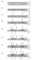
- FIGS. 1 and 2 A specific example of the multilayer substrate manufacturing method of the first aspect will be described with reference to FIGS. 1 and 2 are examples, and the present invention is not limited to the embodiments shown in these drawings.
- FIG. 1 shows an example of a method for manufacturing a build-up multilayer substrate in the case where the metal fine particle assembly layer (S) is formed on all the via conductors (B).
- FIG. 1A shows a build-up layer in which copper foil 2 is laminated on build-up resin 3 on a substrate in which patterned copper foil 2 is laminated on glass epoxy resin 1 which is an insulating layer in step 1 above. The state before L1) is laminated is shown.
- FIG. 1B is a diagram illustrating a state in which the buildup layer (L1) is stacked on the substrate illustrated in FIG. FIG.
- FIG. 1C is a diagram showing a state in which interlayer connection via holes (V1) 11 are formed by performing laser irradiation from the surface side (buildup resin side) of the buildup layer (L1).
- FIG. 1 (d) is a diagram showing a state where a via conductor (B 1) composed of a copper plating portion 4 is formed by performing via fill plating on the via hole (V 1) in step 1 (step 1-1 described later). It is.
- FIG.1 (e) is a figure which shows the state by which the copper foil 2 of the buildup layer (L1) was patterned in the process 1.
- FIG. 1 (f) shows the formation of a metal fine particle assembly layer 5 (S1) by applying a paste containing metal fine particles on the surface of the via conductor (B1) in step 1 (step 1-2 described later) and then heating. It is a figure which shows the state made.
- a buildup layer (L2) in which a copper foil is laminated on the surface of the insulating layer is laminated on the buildup layer (L1) in step 2 (step 2-1 described later).
- step 2 step 2-2 to be described later
- laser beam irradiation is performed from the surface of the buildup layer (L2) to the metal fine particle assembly layer (S1) portion to form an interlayer connection via hole (V2) 11
- FIG. FIG. 1 (h) is a diagram showing a state in which the copper foil is patterned after the via fill plating in step 1 is performed on the via hole (V 2) to form the via conductor (B 2) including the copper plating portion 4. is there.
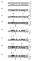
- FIG. 2 shows a case where a defect portion having a radius of curvature of less than 100 ⁇ m or the like exists in the laser irradiation portion on the surface of the via conductor (B), and a metal fine particle assembly layer (S) on the surface of the via conductor (B) where the defect portion exists.
- FIG. 2A shows a build-up layer in which copper foil 2 is laminated on build-up resin 3 on a substrate in which patterned copper foil 2 is laminated on glass epoxy resin 1 which is an insulating layer in step 1 above. The state before L1) is laminated is shown.
- FIG. 1 shows a build-up layer in which copper foil 2 is laminated on build-up resin 3 on a substrate in which patterned copper foil 2 is laminated on glass epoxy resin 1 which is an insulating layer in step 1 above. The state before L1) is laminated.
- FIG. 2B is a diagram illustrating a state in which the buildup layer (L1) is stacked on the substrate illustrated in FIG.
- FIG. 2C is a diagram showing a state in which interlayer connection via holes (V1) 11 are formed by performing laser irradiation from the surface side of the buildup layer (L1).
- FIG. 2D is a diagram showing a state in which the via conductor (B1) including the copper plating portion 4 is formed by performing via fill plating on the via hole (V1) in step 1 (step 1-1 to be described later). It is. Of the formed two via conductors (B1), the defect portion 12 exists in the laser irradiation portion on the surface of one via conductor (B1).
- FIG. 2 (e) is a diagram showing a state in which the copper foil 2 of the buildup layer (L 1) is patterned in step 1.
- FIG. 2 (f) shows a metal fine particle assembly layer (step 1 (step 1-2 to be described later)) after applying a paste containing metal fine particles only on the surface of the via conductor (B1) where defects 12 are present. It is a figure which shows the state which formed S1).
- FIG. 2 (g) shows a buildup layer (L2) obtained by laminating a copper foil on the insulating layer surface on the buildup layer (L1) in step 2 (step 2-1 described later), and then step 2 In (step 2-2 described later), laser beam irradiation is performed from the surface of the buildup layer (L2) to the surface of the metal fine particle assembly layer (S1) and the surface of the via conductor (B1) that does not have a defect, thereby connecting via holes for interlayer connection It is a figure which shows the state which formed (V2) 11.
- FIG. 2 (h) is a diagram showing a state in which the copper foil is patterned after the via fill plating in step 1 is performed on the via hole (V2) to form the via conductor (B2) including the copper plating portion 4. is there.
- Each step will be described below.
- the build-up multilayer substrate is a step of laminating an insulating layer and a build-up layer composed of a copper foil (or copper pattern) conductive layer so that the insulating layer and the conductive layer are alternately arranged.
- This is a substrate manufactured by a sequential lamination method in which via conductors are formed by plating after forming fine interlayer connection via holes having a diameter of about several hundreds of ⁇ m by laser processing or the like.
- the build-up multilayer board has a structure in which insulation layers and conductor layers are built up alternately on the front side or both sides of the conventional printed wiring board called core material (the number of layers is often 2 to 8 layers) and There is a kind of structure in which all layers are made up of build-up layers without using a core material, and the present invention can be applied to any structure.
- the build-up multilayer substrate is a substrate in which an insulator and a pattern are stacked in layers to improve the density of components, and can be a multilayer substrate having several tens of layers.
- step 1 the paste containing metal fine particles is applied on the surface of the via conductor (B1) formed on the buildup layer (L1) in which the copper foil or the copper pattern layer is laminated on the insulating layer surface, and then heated to heat the metal fine particles. This is a step of forming the aggregate layer (S1).
- the via hole for vias (V1) formed in the build-up layer (L1) in which the copper foil or the copper pattern layer is laminated on the insulating layer surface is subjected to via fill plating or via fill plating / polishing to form a via conductor ( B1) forming step (step 1-1), and A step (step 1-2) of forming a metal fine particle aggregate layer (S1) by applying a paste containing metal fine particles on the surface of the via conductor (B1) and heating the paste is included.
- it can carry out either before formation of the said metal microparticle aggregate
- Step 1-1 (A) Build-up layer (L1)
- the buildup layer (L1) is a layer formed by laminating an insulating layer and a conductor layer. As a result of sequentially laminating such a buildup layer (L), the insulating layer and the conductor layer are alternately laminated.
- a built-up multilayer substrate is formed. In the build-up multilayer substrate, via conductors are provided between the interlayers and are formed inside interlayer connection via holes that connect the conductor layers to each other.
- a thermosetting resin such as phenol resin or epoxy resin is usually used.
- imide resin bismaleimide, Triazine resin (BT resin) or the like can be used.
- a glass cloth is usually used in the insulating layer in order to improve the mechanical strength such as load resistance of the laminate.
- Other examples of the substrate include a glass nonwoven fabric and an organic fiber nonwoven fabric.
- A-2) As the copper foil and the laminated board copper foil, for example, a high purity electrolytic copper foil produced by an ordinary electrolysis method is used, and as the laminated board, a copper clad laminated board is usually used.
- a method for producing a laminate for forming the buildup layer (L) for example, a prepreg in a state in which a base material such as glass cloth is impregnated with a semi-cured resin as a resin for forming an insulating layer is used, and a copper foil is used for this
- a method of obtaining a copper-clad laminate in the form of a plate after curing by exhibiting the function of an adhesive when the prepreg is heated and pressed under pressure and heating As a method for producing a laminate for forming the buildup layer (L), for example, a prepreg in a state in which a base material such as glass cloth is impregnated with a semi-cured resin as a resin for forming an insulating layer is used, and a copper foil
- step 1-1 when a copper clad laminate having a copper foil laminated on the insulating layer surface is used as the build-up layer (L), before the via fill plating is performed.
- the copper pattern can be formed by patterning the copper foil, and in step 1-2, the metal fine particle assembly layer (S1) is formed and the copper foil is patterned to form the copper pattern layer. You can also.
- a patterning method of the copper foil in the above step 1-1 for example, a subtractive method in which an unnecessary portion is removed from a laminated board on which the copper foil is stretched to leave a circuit can be employed. In the subtractive method, the part to be left as wiring, etc.
- a mask such as ink or paint that becomes a corrosion-resistant film by silk screen printing, etc.
- a ferric chloride solution having metal corrosiveness This is a method of leaving a copper pattern of a necessary circuit.
- a method of applying a photoresist instead of the masking, covering the wiring pattern shape with a photographed mask film, exposing it to light, dissolving it in a solvent, and etching while leaving the wiring pattern portion can be employed.
- an additive method in which a copper pattern is added to the insulating layer later can also be used.
- (B) Interlayer connection via hole (V1) In the buildup multilayer substrate, it is necessary to connect the conductors of each buildup layer (L) in the plate thickness direction (z direction). For the connection, a through-hole method is widely employed in which an interlayer connection via hole (V1) penetrating each insulating layer is formed and the wall surface of the via hole (V1) is plated. This drilling can be done using a mechanical drill or a laser. Generally, a laser is used for a via hole of 0.1 mm or less. Since the positions and diameters of the holes differ depending on the multilayer substrate, the quality of the holes is important as a base for plating when performing via fill plating.
- B-1) Drilling process For the drilling of the buildup layer (L1), a drilling apparatus is usually used when a mechanical drill is used. In order to open a via of 0.1 mm or less, a carbon dioxide laser drilling machine or the like is used.
- the resin used in the insulating layer is resin due to heat generated by friction during drilling. Melts and flows, and cools and solidifies on the end face of the copper foil to generate a resin smear.
- the removal of the resin smear can be performed by a desmear process. For example, when a build-up multilayer substrate is manufactured, if a hole is drilled with a carbon dioxide laser or the like, smear remains at the bottom of the via, so it is also necessary to remove the smear in the via.
- the desmear treatment swells the resin by the conditioner treatment, and then treats with alkaline permanganate, so that the epoxy resin is dissolved and the inside of the via and the end of the copper foil Is cleaned.
- the surface of the electrolyte is made conductive by plating, and a plated layer by electrolytic plating is formed thereon to form the via conductor (B1).
- plating is formed not only in the hole, but also on the copper foil or copper pattern in the vicinity of the hole. Therefore, when the via conductor (B1) is formed, the surface direction ( The conductor pattern in the xy direction) and the three-dimensional conductor connection in the via hole direction (z direction) are performed in parallel.
- plating is performed by immersing in a plating bath, it is necessary to form a plating resist on the part where the plating is not attached to the surface of the buildup layer (L), if necessary, before the plating process.
- Electroless plating i) Electroless plating
- Pretreatments include, for example, conditioning (improves the wettability of the hole wall by surface treatment with a surfactant or the like), microetching (copper foil surface with an etching agent) Slight dissolution and removal), characterization (immersion in a characterization solution containing a palladium-tin complex salt to adsorb the catalyst), and acceleration (removal of tin unnecessary for the action of the palladium catalyst) are sequentially performed.
- the electroless plating production panel is immersed in an electroless plating bath to deposit copper in the hole and on the copper foil surface.
- Formalin is usually used as a reducing agent for copper ions in the electroless plating solution.
- Electroplating is performed by employing a pattern plating method for limiting the portion to be electroplated by using an electroplating plating resist, a panel plating method for plating the surface without using a resist, or the like.
- step 1-2 a paste containing metal fine particles is applied and heated on the surface of the via conductor (B1) to form a metal fine particle aggregate layer (S1) or a metal fine particle aggregate layer (S1). Later, the copper foil part is patterned.
- step 1-2 a paste containing metal fine particles is applied and heated on the surface of the via conductor (B1) to form a metal fine particle aggregate layer (S1) or a metal fine particle aggregate layer (S1). Later, the copper foil part is patterned.
- V2 via hole
- the laser beam penetrates the insulating layer of the buildup layer (L2).
- the paste containing fine metal particles is 10 to 80% by mass of fine metal particles and the following dispersion media 20 to 90 in consideration of the viscosity at the time of coating, the aggregation properties, the formation of the fine metal particle assembly layer (S1), and the like. It is preferably composed of mass%.
- the blending amount of the metal fine particles is small, the film thickness after heating becomes thin, so that in order to obtain a sufficient effect on the reflectance and the radius of curvature, it is necessary to apply the layers repeatedly and lack practicality.
- the amount of the metal fine particles is large, it may be difficult to apply on the substrate or the smoothness of the surface may be lowered due to an excessive viscosity.
- a binder resin and a dispersing agent can be arbitrarily mix
- metal fine particles examples include copper, silver, gold, tin, etc. having high conductivity, or copper alloys containing one or more selected from these metals. Among these, copper or a copper alloy is preferable. When using copper particles, some of the particles may be oxidized, for example, the entire or part of the particle surface may be oxidized.
- the X-ray diffraction peak intensity ratio (H2 / [H1 + H2]) is 0 when the peak height of the Cu (111) plane is H1 and the peak height of the Cu 2 O (111) plane is H2. When it is .67 or more and 0.91 or less, baking can be performed for a short time.
- the average particle diameter of the metal fine particles is preferably 10 to 300 nm in consideration of control of the reflectance of the laser beam and the radius of curvature of the laser irradiation part.
- A-2 Paste Dispersion Medium As the dispersion medium of the paste, a reducing solvent containing a polyol component is preferable. As the reducing solvent component, in addition to the polyol, the dispersibility of the paste is improved and the baking is facilitated. Therefore, a compound having an amide group, an ether compound, an alcohol, a ketone compound, an amine compound, and the like can be blended.
- Polyol polyol is a polyol having two or more hydroxyl groups in the molecule and having a boiling point in the range of 100 to 350 ° C. at normal pressure. Polyols form liquid and / or vaporized, reducing atmospheres when firing fine metal particles such as copper and copper alloys, and as a result, promote the reduction and firing of fine metal particles such as copper and copper alloys. Demonstrate the effect.
- polyols examples include ethylene glycol, diethylene glycol, polyethylene glycol, glycerin, 1,2-propanediol, 1,3-propanediol, 1,2-butanediol, 1,3-butanediol, 1,4-butanediol, -Butene-1,4-diol, pentanediol, hexanediol, octanediol, 1,1,1-trishydroxymethylethane, 2-ethyl-2-hydroxymethyl-1,3-propanediol, 1,2,6 -Hexanetriol, 1,2,3-hexanetriol, 1,2,4-butanetriol, threitol, erythritol, pentaerythritol, xylitol, sorbitol, pentitol, terpineol, and hexitol.
- polyols usable in the present invention is not limited to the polyols exemplified above. These polyols are thermally decomposed when metal fine particles such as copper and copper alloys are baked to generate hydrogen radicals, and the hydrogen radicals exhibit a function to reduce or prevent oxidation of the oxide film on the surface of the metal fine particles. In addition, it is possible to form a highly conductive metal film with good firing even with base metal fine particles, and to enable firing at a relatively low temperature.
- a compound having an amide group, an ether compound, an alcohol, a ketone compound, an amine compound, and the like described below may be further blended. It can.
- the compound having an amide group include N-methylacetamide, N-methylformamide, N-methylpropanamide, formamide, N, N-dimethylacetamide, 1,3-dimethyl-2-imidazolidinone, N, N— Examples thereof include one or more selected from dimethylformamide, 1-methyl-2-pyrrolidone, hexamethylphosphoric triamide, 2-pyrrolidinone, ⁇ -caprolactam, and acetamide.
- R 1 —O—R 2 (where R 1 and R 2 are each an independent alkyl group having 1 to 4 carbon atoms)
- An alcohol represented by the formula R 3 —OH (R 3 is an alkyl group having 1 to 4 carbon atoms)
- R 4 —C ( ⁇ O) —R 5 (R 4 , R 5 are A ketone compound represented by an independent alkyl group having 1 to 2 carbon atoms)
- R 6 — (N—R 7 ) —R 8 (R 6 , R 7 , R 8 Are each independently an alkyl group or hydrogen, and has 0 to 2 carbon atoms.)
- the ether compound are selected from diethyl ether, methyl propyl ether, dipropyl ether, diisopropyl ether, methyl-t-butyl ether, t-amyl methyl ether, divinyl ether, ethyl vinyl ether, and allyl ether.
- the alcohol include one or two selected from methanol, ethanol, 1-propanol, 2-propanol, 2-butanol, and 2-methyl 2-propanol. More than one species can be exemplified, and specific examples of the ketone compound include one or more selected from acetone, methyl ethyl ketone, and diethyl ketone.
- Specific examples of the amine compound include triethylamine and / or Or diethylamine It can be exemplified.
- Binder resin improves the dispersibility and dispersion stability of metal fine particles such as copper and copper alloy in the paste and facilitates the viscosity adjustment of the paste.
- the binder resin is selected from cellulose resin binder, acetate resin binder, acrylic resin binder, urethane resin binder, polyvinyl pyrrolidone resin binder, polyamide resin binder, butyral resin binder, and terpene binder. 1 type (s) or 2 or more types can be used.
- the above paste can contain a dispersant for metal fine particles such as copper and copper alloy.
- the dispersant covers at least a part of the surface of the metal fine particles in the paste and exerts an action of dispersing the metal fine particles in a state where the secondary aggregation property is small.
- Preferred as the dispersant is a water-soluble polymer compound, an amine polymer such as polyvinyl pyrrolidone, N-vinyl pyrrolidone, or polyethyleneimine; a hydrocarbon polymer having a carboxylic acid group such as polyacrylic acid or carboxymethyl cellulose.
- Polymer acrylamide such as polyacrylamide; one or more selected from polyvinyl alcohol, polyethylene oxide, starch, and gelatin.
- A-3) Production of Paste Containing Metal Fine Particles When producing a paste containing metal fine particles, the metal fine particles and the dispersion medium are mixed and then kneaded by applying shear stress to prepare a paste.
- a kneader such as a kneader or a three-roller
- a reiki machine that can be kneaded in a closed system, a kneader, or the like can be used.
- kneading it is preferable to carry out, for example, in an inert gas atmosphere so that oxidation of copper powder or the like does not proceed excessively.
- the application is not particularly limited, and printing methods such as screen printing, mask printing, spray coating, bar coating, knife coating, spin coating, ink jet printing, and dispenser printing, or transfer methods using stamps, needles, etc. Can be used.
- a pattern having a diameter of about 10 to 500 ⁇ m can be formed.
- a known method can be adopted for these discharge, application, or transfer means.
- the radius of curvature of the laser irradiation portion on the surface of the via conductor (B1) is measured in advance, and the via conductor (B1 including the defect portion only when there is a defect portion having a curvature radius of less than 100 ⁇ m) ) Applying a pace on the surface, and after heating, forming a metal fine particle assembly layer (S1) to be described later, the defect portion can be repaired, and the radius of curvature of the laser irradiation portion can be made 100 ⁇ m or more. . (B-2) Paste heating
- the metal fine particle aggregate layer can be formed by applying a paste containing metal fine particles on the via conductor (B1) surface and the like and then heating.
- the metal fine particle aggregate layer is an aggregate formed by collecting the remaining metal fine particles in the process of heating the paste and removing the dispersion solvent, and the metal fine particle surfaces are fused to each other by heating. Sintered body formed and the surface of the metal fine particles are not fused to each other by heating, but the attractive force between particles generated due to the extremely small particle size of the metal fine particles, or the resin and residual dispersion in the paste Both non-sintered aggregates formed by aggregation of metal fine particles by the formation of an adhesive substance caused by the medium are included. In order to prevent oxidation of the metal fine particles in the metal fine particle aggregate layer, it is desirable to heat in a furnace in a nitrogen atmosphere, for example.
- heating can be performed at 100 to 200 ° C., selected from the range of 10 seconds to 10 minutes depending on the type of solvent and the amount of paste applied.
- the paste can be fired by heating to form a metal fine particle aggregate layer.
- firing conditions for example, heating can be performed at about 200 to 300 ° C. for about 10 to 60 minutes.
- heating in multiple temperature steps may be performed in advance, for example, by drying the paste at a low temperature of about 100 ° C. and then baking at about 200 to 300 ° C.
- a known method such as a method of irradiating light using a laser beam or a halogen lamp, a method of blowing hot air, a method of using a hot plate, or the like can be used. .
- the laser beam reflectance on the surface of the laser irradiated portion in the metal fine particle aggregate layer (S1) formed on the via conductor (B1) by the above method is the same as before the formation of the aggregate layer. It is preferable that it is lower than the laser light reflectance of the surface of the via conductor (B1) formed by electrolytic plating. Specifically, the laser beam on the surface of the metal fine particle assembly layer (S1) is reflected when the wavelength of the laser beam used for forming the via hole (V2), for example, in the range of 0.2 to 11.0 ⁇ m is reflected.
- the light reflectance is preferably 20% or less.
- the laser light reflectance on the surface of the metal fine particle assembly layer (S1) exceeds 20%, the wall surface of the via hole (V2) formed in the buildup layer (L2) by the incident light of the laser is damaged by the reflected light. There is a risk that resin smear will increase. From this viewpoint, it is more preferable that the laser beam reflectance on the surface of the metal fine particle assembly layer (S1) is 15% or less.
- the laser light reflectance on the surface of the laser irradiation portion in the metal fine particle assembly layer (S1) is controlled by the type of metal of the metal fine particles to be blended in the paste, the average particle diameter in the aggregate structure, and the heating temperature and heating time Is possible.
- the reflectance is reduced when copper is selected as the metal fine particle rather than gold or silver.
- a desired reflectance can be realized by optimizing heating conditions such as temperature and time.
- a general reflectance measuring device eg, JASCO Corporation, Micro-UV Visible Near-Infrared Spectrophotometer (Model: MSV-5000)
- MSV-5000 Micro-UV Visible Near-Infrared Spectrophotometer
- the radius of curvature of the surface of the laser irradiation part in the metal fine particle assembly layer (S1) formed on the via conductor (B1) is preferably 100 ⁇ m or more, and more preferably 150 ⁇ m or more. Further, in order to prevent the laser beam from being reflected and damaged on the wall surface of the via hole (V2), it is desirable that the laser beam is reflected in the incident direction. Although it is desirable that it is flat, that is, the radius of curvature is infinite, in reality, it is limited by the processing accuracy.
- the radius of curvature is a macro curvature radius that damages the nearby via-hole wall surface by randomly changing the direction of reflection when the laser beam is irradiated on the surface of the metal fine particle assembly in drilling with laser light.
- step 1 via fill plating is performed on the interlayer connection via hole (V1). After electroless plating, copper ions in the electrolytic bath are reduced and grow from the electroless plating layer when electrolytic plating is performed. However, irregularities may occur on the surface of the via conductor (B1) formed by the plating, and such a defective portion is formed in a portion irradiated with laser light when forming the via hole (V2). As a result, the wall surface of the via hole (V2) formed in the build-up layer (L2) due to the reflection of the laser beam may be damaged and the resin smear may increase.
- the laser light irradiation portion on the surface of the via conductor (B1) By forming the metal fine particle assembly layer (S1) in a portion having a radius of curvature of less than 100 ⁇ m, the radius of curvature of the laser irradiation portion surface is set to 100 ⁇ m or more, or the reflectance of the laser beam on the laser irradiation portion surface is 20%. By making the following, such inconvenience is remarkably suppressed. From this viewpoint, the radius of curvature is more preferably 150 ⁇ m or more.
- the radius of curvature of the surface of the laser irradiation part depends on the paste shape when the paste is applied on the substrate, and can be controlled by the mixing ratio of the dispersion medium in the paste, the paste viscosity, and the like.
- the measurement of the curvature radius of the laser irradiation part surface can be performed using a three-dimensional surface shape measuring machine (for example, ZYGO Co., Ltd., model: NewView7200).
- the average particle diameter of the aggregate particles in the metal fine particle aggregate layer (S1) is preferably 10 to 300 nm.
- the via hole (V2) is formed on the aggregate by plating in Step 4 below, if the particle size is smaller than this range, the surface is smoothed and the anchor effect is insufficient at the plating interface. Moreover, since the clearance gap between aggregate grains causes the void of a plating interface when it is large, adhesiveness falls.
- Step 2 the metal fine particle assembly layer (S1) is irradiated with laser from the surface of the buildup layer (L2) formed on the buildup layer (L1) and having a copper foil or copper pattern layer laminated on the insulating layer surface.
- Step 2 includes a step of laminating a buildup layer (L2) in which a copper foil or a copper pattern layer is laminated on the surface of the insulating layer on the buildup layer (L1) (step 2-1), and a buildup layer (L2). It includes a step (step 2-2) of forming a via hole (V2) for interlayer connection by irradiating the metal fine particle assembly layer (S1) from the surface with laser.
- the build-up layer (L) includes a build-up layer made of a prepreg made of glass epoxy resin and a copper foil, and a build-up made by laminating a copper foil via an adhesive layer on an insulating layer made of glass epoxy resin.
- the layers can be stacked.
- Step 2-1 A buildup layer precursor composed of at least an inorganic filler and a resin is temporarily laminated on the laminated buildup layer (L1) obtained by press curing of a prepreg. And this buildup layer precursor can be adhere
- the buildup layer (L2) in which the copper foil is laminated on the insulating layer surface can be laminated on the laminated buildup layer (L1) by the adhesive layer via the adhesive layer.
- the adhesive layer can be formed, for example, by curing an acrylic or epoxy adhesive.
- the surface of the build-up layer (L1) can be subjected to a roughening treatment. By this roughening treatment, carbon dioxide gas (CO 2 ) on the copper surface. While the absorptance of laser light (wavelength: about 9.8 ⁇ m) is increased, the resistance to laser processing may be reduced.
- Step 2-2 laser irradiation is performed from the surface of the buildup layer (L2) toward the metal fine particle assembly layer (S1) to form an interlayer connection via hole (V2). Laser irradiation is as described above.
- the laser light reflectance is in the range of 0.2 to 11.0 ⁇ m, or the laser light reflectance of the laser light used for forming the via hole (V2) is 20% or less, or a process In the metal fine particle assembly layer (S1) formed in step 2, the radius of curvature of the laser-irradiated portion surface can be made 100 ⁇ m or more, and the generation of defects in the via holes for interlayer connection caused by the surface defects of via fill plating can be suppressed. Or by improving the formation of the metal fine particle assembly layer (S1), if necessary, to improve the yield in manufacturing the build-up multilayer substrate It becomes possible.
- the build-up multilayer substrate according to the second aspect of the present invention is obtained by via-fill-plating an interlayer connection via hole (V) formed by laser processing on a build-up layer (L) in which a copper pattern layer is laminated on the insulating layer surface.
- a pair of via conductors adjacent to each other in the thickness direction including at least one buildup layer (L) in which a via conductor (B) is formed and a metal fine particle sintered body layer (S) is further formed on the plating surface ( B) It is a structure in which the two are connected continuously (via-on-via structure).
- the build-up layer (L), the interlayer connection via hole (V), and the via conductor (B) in the build-up multilayer substrate of the second mode are as described in the first mode. It is the same as the contents.
- Metal fine particle assembly layer (S) The metal fine particle assembly layer (S) formed on the surface of the laser irradiation portion in the via conductor (B) has a wavelength of 0.2 to 11.0 ⁇ m, or a range of laser light used for forming the via hole (V). The laser light reflectance is preferably 20% or less, more preferably 15% or less.
- the average particle diameter of the aggregate particles in the metal fine particle aggregate layer (S) is preferably 10 to 300 nm.
- the via hole (V) is formed on the metal fine particle assembly layer (S) by plating, if the particle diameter is less than the above range, the surface is smoothed, and the anchor effect is insufficient at the plating interface.
- the gaps between the aggregated grains cause voids at the plating interface, which may reduce the adhesion.
- Paste 1 Paste containing copper fine particles
- the metal fine particles copper fine particles having an average primary particle diameter of 30 nm were used.
- This copper particle has an X-ray diffraction peak intensity ratio (H2 / [H1 + H2) where the peak height of the Cu (111) plane is H1 and the peak height of the Cu 2 O (111) plane is H2 in the X-ray diffraction measurement. ]) Is 0, and it has not been confirmed that it is oxidized.
- the composition of the paste 1 is composed of 50% by mass of copper fine particles and 50% by mass of glycerin (dispersion medium).
- Paste 2 low concentration paste containing copper fine particles
- copper fine particles having an average primary particle diameter of 30 nm were used.
- This copper particle has an X-ray diffraction peak intensity ratio (H2 / [H1 + H2) where the peak height of the Cu (111) plane is H1 and the peak height of the Cu 2 O (111) plane is H2 in the X-ray diffraction measurement. ]) Is 0, and it has not been confirmed that it is oxidized.
- the composition of the paste 2 is composed of 10% by mass of copper fine particles and 90% by mass of glycerin (dispersion medium).
- Paste 3 (Paste containing silver fine particles) Silver fine particles having an average primary particle diameter of 10 nm were used as the metal fine particles.
- the composition of the paste 2 is composed of 50% by mass of silver fine particles and 50% by mass of tetradecane (dispersion medium).
- Paste 4 (paste containing copper particles partially oxidized) As the metal fine particles, copper fine particles having an average primary particle diameter of 30 nm and partially oxidized on the surface and the like were used.
- This copper particle has an X-ray diffraction peak intensity ratio (H2 / [H1 + H2) where the peak height of the Cu (111) plane is H1 and the peak height of the Cu 2 O (111) plane is H2 in the X-ray diffraction measurement. ]) was 0.8, and it was confirmed that a part was oxidized.
- the composition of the paste 4 is composed of 50% by mass of copper fine particles and 50% by mass of glycerin (dispersion medium).
- Electrolytic plating After immersing in the electroless plating pre-characterizing solution, characterization and acceleration including the complex compound of palladium-tin are performed, and the plating bath composition including copper sulfate and chelating agent is reduced. Electroless plating was performed using formalin as an agent. (B) Electrolytic plating Electrolytic plating using an electroless plating layer as a base layer was performed to form via conductors in interlayer connection vias.
- the electrolytic plating solution is manufactured by Ebara Eugene Co., Ltd., having a copper sulfate pentahydrate concentration of 230 g / L, a sulfuric acid concentration of 70 g / L, and a chlorine ion concentration of 60 mg / L (trade name: Cubelite VF). -MU) was added at 20 ml / L. (3) Drilling of interlayer connection vias Using a UV laser (wavelength: 355 nm), interlayer connection vias with a diameter of 50 ⁇ m were formed.
- Embodiment 1 will be described below with reference to FIGS. 1 (a) to 1 (h).
- First buildup layer formation First buildup in which a copper foil is laminated on the surface of an insulating layer on a copper pattern layer (see FIG. 1A) formed on a substrate (glass epoxy resin). Layers are stacked (see FIG. 1 (b)), and from the surface of the buildup layer, the surface of the copper pattern of the substrate is irradiated with a UV laser having a wavelength of 355 nm to form four first via holes for interlayer connection having a diameter of 50 ⁇ m. (Refer to FIG. 1C, where two via holes are shown. The same applies hereinafter).
- the interlayer connection via hole portion was subjected to electroless plating, electrolytic plating, and polishing treatment to form a first via conductor made of copper plating (see FIG. 1D).
- the copper pattern layer was formed by the subtractive method (refer FIG.1 (e)).
- Via fill plating was performed on the via hole to form a second via conductor made of copper plating, and a copper pattern layer was formed by etching the copper foil (sample number: 1-1 in Table 1) (FIG. 1 ( h)).
- a copper pattern layer was formed by etching the copper foil (sample number: 1-1 in Table 1) (FIG. 1 ( h)).
- (3) In order to evaluate the yield, build-up multilayer substrate samples were further prototyped nine times by the methods (1) to (2) (sample numbers: 1-2 to 10), and a total of 10 samples were prepared. As a result of evaluating the shape of the second via hole in each sample, the yield was 100% because all four samples were good (Good).
- Example 1 (1) Formation of first build-up layer The first layer was formed on the substrate in the same manner as described in Example 1. (2) Formation of second buildup layer A second buildup layer is formed on the first buildup layer in the same manner as in Example 1 except that the paste 1 is not applied and fired on the plating surface. (Corresponding to FIG. 1 (h) of Example 1) (sample number: 2-1 in Table 1). For sample number: 2-1, if the evaluation of the second via hole shape corresponding to FIG. 1 (g) of the first embodiment shows that a failure (Not good) is included, the second build-up is performed. No via fill plating of the layer was performed.
- Example 2 A second embodiment will be described below with reference to FIGS. 2 (a) to 2 (h).
- (1) Formation of first buildup layer A first buildup layer was formed on a substrate (see FIG. 2A) in the same manner as described in Example 1 (see FIG. 2B). ). From the surface side of the first buildup layer, the surface of the copper pattern was irradiated with a UV laser having a wavelength of 355 nm to form four first via holes 11 for interlayer connection having a diameter of 50 ⁇ m (see FIG. 2C). In the figure, two via holes are shown (the same applies hereinafter).
- the electroless plating, electrolytic plating, and polishing treatment were performed on the via hole for interlayer connection to form a via conductor made of copper plating (see FIG. 2D).
- a copper pattern layer was formed by a subtractive method for the copper foil portion of the first buildup layer (see FIG. 2 (e)).
- Example 3 A build-up multilayer substrate was prepared as described in Example 2, except that paste 2 (low concentration paste containing copper fine particles) was used instead of paste 1 (paste containing copper fine particles).
- paste 2 low concentration paste containing copper fine particles
- paste 1 paste containing copper fine particles
- Example 4 A build-up multilayer substrate was prepared as described in Example 2, except that paste 3 containing silver fine particles was used instead of paste containing copper fine particles (paste 1).
- (1) Formation of first buildup layer A first buildup layer was formed on a substrate in the same manner as described in Example 1.
- Second build-up layer formation As described in Example 2 except that paste 3 (low concentration paste containing silver fine particles) was applied instead of paste 1 (paste containing copper fine particles).
- a second buildup layer was formed on the first buildup layer in the same manner as described above (sample number: 5-1 in Table 2). Similarly to Example 2, the results of evaluating the second via hole shape in the process corresponding to FIG. 2G of Example 2 were all good (Good).
- Example 5 A build-up multilayer substrate was prepared as described in Example 1, except that paste 4 (a paste containing copper fine particles partially oxidized) was used instead of paste 1 (a paste containing copper fine particles). .
- (1) Formation of first buildup layer A first buildup layer was formed on a substrate in the same manner as described in Example 1.
- Second buildup layer formation As described in Example 1, except that paste 2 (a low concentration paste containing copper fine particles) was applied instead of paste 1 (a paste containing copper fine particles).
- a second buildup layer was formed on the substrate as shown in Table 3 (sample number: 6-1 in Table 2). Similar to Example 2, the results of evaluating the second via hole shape in the process corresponding to FIG. 2G of Example 1 were all good (Good).
- Example 3 A build-up multilayer substrate sample was further prototyped 9 times by the same method as described in Example 1 to produce a total of 10 samples (sample numbers: 6-2 to 10). As a result of evaluating the yield, the yield was 100%. The results are summarized in Table 3.
- Example 6 A build-up multilayer substrate was produced as described in Example 5, except that the paste was fired with a laser.
- (1) Formation of first buildup layer A first buildup layer was formed on a substrate in the same manner as described in Example 1.
- (2) Formation of the second buildup layer The second buildup layer was formed on the substrate as shown in Table 3 in the same manner as described in Example 5 except that the paste was fired with a laser. (Sample number: 7-1 in Table 3).
- the laser conditions were a wavelength of 980 nm, an irradiation diameter of 800 ⁇ m on the sample surface, an output of 1 W, and an irradiation time of 100 ms.
- a nozzle having a diameter of 5 mm was disposed at a position 10 mm away from the firing part, and nitrogen was flowed at a flow rate of 1 L / min. Similar to Example 2, the results of evaluating the second via hole shape in the process corresponding to FIG. 2G of Example 1 were all good (Good). (3) A build-up multilayer substrate sample was further prototyped 9 times by the same method as described in Example 2 to produce a total of 10 samples (sample numbers: 7-2 to 10). As a result of evaluating the yield, the yield was 100%. The results are summarized in Table 3.
- the metal fine particle sintered body layer formed in step 2 of the first aspect of the present invention is formed by the method of (1) to (2) of Example 1. A new sample prepared up to the process was newly prepared, and the average particle size was evaluated using the above-described average particle size evaluation method for the metal fine particle sintered body layer. The average particle size of the particles was 100 nm ⁇ 10 nm.
Landscapes
- Engineering & Computer Science (AREA)
- Manufacturing & Machinery (AREA)
- Microelectronics & Electronic Packaging (AREA)
- Production Of Multi-Layered Print Wiring Board (AREA)
Abstract
歩留まり向上が可能なビルドアップ多層基板の製造方法を提供する。 絶縁層表面に銅箔又は銅パターン層を積層したビルドアップ層(L1)に形成されたビア導体(B1)表面上に、金属微粒子を含むペーストを塗布後加熱して、金属微粒子集合体層(S1)を形成する工程(工程1)と、ビルドアップ層(L1)上に形成され、絶縁層表面に銅箔又は銅パターン層が積層されたビルドアップ層(L2)表面から金属微粒子集合体層(S1)部にレーザー照射を行って、層間接続用ビアホール(V2)を形成する工程(工程2)を含む、ビルドアップ多層基板の製造方法。
Description
本発明は、ビルドアップ工法によるビルドアップ多層基板の製造方法、及び該製造方法により得られるビルドアップ多層基板に関する。
近年、電子機器の小型化および高機能化の要求がますます高まっている。プリント配線板に対する高密度実装の要求に対応するために、微細な回路配線パターンを設けることにより高密度実装が可能なビルドアップ型の多層基板が知られている。
ビルドアップ型多層基板は、一般的には、スルーホールを有する多層プリント配線板をコア基板とし、このコア基板の両面若しくは片面に1~2層程度のビルドアップ層を設けたものが多く使用されている。このビルドアップ多層基板は、一般に基板上の回路と、ビルドアップ層上の回路とを電気的に接続する有底型の層間接続用のビア導体部を備えている。このビア導体部は、ビルドアップ層を貫通してビアホールの内壁に形成されためっき層から構成される層間導体である。
ビルドアップ型多層基板は、一般的には、スルーホールを有する多層プリント配線板をコア基板とし、このコア基板の両面若しくは片面に1~2層程度のビルドアップ層を設けたものが多く使用されている。このビルドアップ多層基板は、一般に基板上の回路と、ビルドアップ層上の回路とを電気的に接続する有底型の層間接続用のビア導体部を備えている。このビア導体部は、ビルドアップ層を貫通してビアホールの内壁に形成されためっき層から構成される層間導体である。
ビアホールにおいてはレーザー加工の条件で微細化、小径化、信頼性向上が図られ、特にレーザー加工においては生産性向上につながることから近年重要視されている。ビルドアップ多層基板には、逐次積層法により絶縁層、導電層を順次積み上げ、直径数百μm程度の微細な層間接続ビアホールが形成されるので、ドリル加工技術では形成不可能な0.1mm以下の小径穴の加工がレーザー加工技術の応用により行われてきている。また、ビルドアップ多層基板においては、導体層と導体層とを導通させるビアとその上層のビアとを近接して配置するビアオンビア構造が用いられることがあるが、ビアオンビア構造をレーザー加工により形成する場合、レーザーの照射により上層基板が貫通した際に、下層基板のビア表面にもレーザーが照射されるため、レーザー光の乱反射が起きた場合にビアホールの壁面が損傷し、ホール形状が変形することがある。
特許文献1には、配線パターンのファイン化、導通性に優れた、内部が充填された第1ビアと、第1ビアより大径の第2ビアが第1ビアの外周の1/2以上を覆って形成されている配線基板のビアオンビア構造が開示されている。
特許文献2には、レーザー法により、外層銅箔から銅箔回路層の層間導通を確保するために用いるスルーホール、ビアホールを形成する貫通孔若しくは凹部を形成するために用いる銅張積層板において、当該銅張積層板の外層銅箔表面におけるレーザー光の反射率が86%以下であることを特徴とするレーザー加工用の銅張積層板が開示され、実施例においてレーザー光反射率が71~81%であったことが示されている。
特許文献2には、レーザー法により、外層銅箔から銅箔回路層の層間導通を確保するために用いるスルーホール、ビアホールを形成する貫通孔若しくは凹部を形成するために用いる銅張積層板において、当該銅張積層板の外層銅箔表面におけるレーザー光の反射率が86%以下であることを特徴とするレーザー加工用の銅張積層板が開示され、実施例においてレーザー光反射率が71~81%であったことが示されている。
特許文献3には、銅箔の一方の面の表面粗さ(Rz)が2μm以下で、レーザーを反射する平滑面であり、該平滑面を樹脂基材と接着することを特徴とする銅箔が開示されている。
また、特許文献4には、プラスチックフィルム層、該プラスチックフィルム層上に形成された離型層及び該離型層上に形成された金属膜層を有する金属膜付きフィルムにおいて、プラスチックフィルム層上よりレーザーを照射して、ブラインドビアを形成する工程を含む、回路基板の製造方法が開示されている。
また、特許文献4には、プラスチックフィルム層、該プラスチックフィルム層上に形成された離型層及び該離型層上に形成された金属膜層を有する金属膜付きフィルムにおいて、プラスチックフィルム層上よりレーザーを照射して、ブラインドビアを形成する工程を含む、回路基板の製造方法が開示されている。
絶縁層表面に銅箔が積層されたビルドアップ層を積層し、レーザー光を照射して該絶縁層にビアオンビア構造等を形成するためのビアホールを設ける際に、絶縁層を貫通した直後に、照射される下層ビア表面のレーザー光表面反射率が高いか、又はレーザー光の乱反射が多い場合には絶縁層に設けられるビアホール壁面に欠陥又は樹脂スミア(resin smear、樹脂よごれ)が多く発生するおそれがある。ビルドアップ多層基板の製造は、ビルドアップ層の積層、ビアホールの形成、めっき、銅箔のパターニング等多くの工程を経るので、製品の歩留まりを向上させることは極めて重要である。
上記従来技術において、絶縁層を貫通して照射されるレーザー光について、ビアホール形成が完了した直後に生じる下層ビア表面での反射を簡便な方法で制御して、製品の歩留まりを向上させるために更なる改良が求められている。
本発明は、ビルドアップ多層基板の製造において、ビアホール形成の際に、絶縁層を貫通して照射される銅層表面のレーザー光反射率を低下させるか、又はビアフィルめっき後にその表面欠陥に基づく曲率半径の小さい凹部形状等が生じていても修復により、歩留まりを向上させることが可能なビルドアップ多層基板の製造方法、及び該製造方法により得られるビルドアップ多層基板を提供することを目的とする。
本発明は、ビルドアップ多層基板の製造において、ビアホール形成の際に、絶縁層を貫通して照射される銅層表面のレーザー光反射率を低下させるか、又はビアフィルめっき後にその表面欠陥に基づく曲率半径の小さい凹部形状等が生じていても修復により、歩留まりを向上させることが可能なビルドアップ多層基板の製造方法、及び該製造方法により得られるビルドアップ多層基板を提供することを目的とする。
本発明者等は、上記課題に鑑み鋭意検討した結果、ビルドアップ層に形成したビア導体の表面上に、金属微粒子を含むペーストを塗布後加熱して金属微粒子集合体層を形成し、該金属微粒子集合体層上に更にビルドアップ層を積層した後に、該ビルドアップ層から金属微粒子集合体層部にレーザー光を照射してビアホールを設けることにより、上記課題が解決できることを見出し、本発明を完成させるに至った。
すなわち本発明は、以下の(1)ないし(11)に記載する発明を要旨とする。
すなわち本発明は、以下の(1)ないし(11)に記載する発明を要旨とする。
(1)ビルドアップ多層基板の製造方法であって、
絶縁層表面に銅箔又は銅パターン層を積層したビルドアップ層(L1)に形成されたビア導体(B1)表面上に、金属微粒子を含むペーストを塗布後加熱して、金属微粒子集合体層(S1)を形成する工程(工程1)と、
ビルドアップ層(L1)上に形成され、絶縁層表面に銅箔又は銅パターン層が積層されたビルドアップ層(L2)表面から金属微粒子集合体層(S1)部にレーザー照射を行って、層間接続用ビアホール(V2)を形成する工程(工程2)を含むことを特徴とする、ビルドアップ多層基板の製造方法(以下、第1の態様ということがある)。
(2)前記金属微粒子集合体層(S1)におけるレーザー照射部表面の、レーザー光の0.2~11.0μmの波長範囲における反射率、又は前記ビアホール(V2)形成に使用するレーザー光の波長における反射率が20%以下であることを特徴とする、前記(1)に記載のビルドアップ多層基板の製造方法。
(3)前記金属微粒子集合体層(S1)におけるレーザー照射部表面の曲率半径が100μm以上であることを特徴とする、前記(1)に記載のビルドアップ多層基板の製造方法。
(4)前記ビア導体(B1)が、前記ビルドアップ層(L1)に形成された層間ビアホール(V1)にビアフィルめっき、又はビアフィルめっき後に研磨を行って形成された導体であることを特徴とする、前記(1)から(3)のいずれかに記載のビルドアップ多層基板の製造方法。
絶縁層表面に銅箔又は銅パターン層を積層したビルドアップ層(L1)に形成されたビア導体(B1)表面上に、金属微粒子を含むペーストを塗布後加熱して、金属微粒子集合体層(S1)を形成する工程(工程1)と、
ビルドアップ層(L1)上に形成され、絶縁層表面に銅箔又は銅パターン層が積層されたビルドアップ層(L2)表面から金属微粒子集合体層(S1)部にレーザー照射を行って、層間接続用ビアホール(V2)を形成する工程(工程2)を含むことを特徴とする、ビルドアップ多層基板の製造方法(以下、第1の態様ということがある)。
(2)前記金属微粒子集合体層(S1)におけるレーザー照射部表面の、レーザー光の0.2~11.0μmの波長範囲における反射率、又は前記ビアホール(V2)形成に使用するレーザー光の波長における反射率が20%以下であることを特徴とする、前記(1)に記載のビルドアップ多層基板の製造方法。
(3)前記金属微粒子集合体層(S1)におけるレーザー照射部表面の曲率半径が100μm以上であることを特徴とする、前記(1)に記載のビルドアップ多層基板の製造方法。
(4)前記ビア導体(B1)が、前記ビルドアップ層(L1)に形成された層間ビアホール(V1)にビアフィルめっき、又はビアフィルめっき後に研磨を行って形成された導体であることを特徴とする、前記(1)から(3)のいずれかに記載のビルドアップ多層基板の製造方法。
(5)前記工程2で形成された、ビルドアップ層(L2)の層間接続用ビアホール(V2)にビアフィルめっき、又はビアフィルめっき後研磨を行ってビア導体(B2)を形成し(工程1’)、
更に前記工程1と工程2を、1回又は2回以上繰り返し行ってビルドアップ層(L)を積層することを特徴とする前記(1)から(4)のいずれかに記載のビルドアップ多層基板の製造方法。
(6)前記工程2のビルドアップ層(L1)が基板上に形成されていることを特徴とする、前記(1)から(5)のいずれかに記載のビルドアップ多層基板の製造方法。
(7)前記工程1で形成されるいずれかの金属微粒子集合体層(S1)のレーザー照射部表面のレーザー光反射率が、ビアフィルめっき後、又はビアフィルめっき・研磨後の、レーザー照射部に対応するめっき表面のレーザー光反射率より低下していることを特徴とする、前記(1)から(6)のいずれかに記載の多層基板の製造方法。
(8)前記工程1で形成されるいずれかの金属微粒子集合体層(S1)におけるレーザー照射部表面の、レーザー光の0.2~11.0μmの波長範囲でのレーザー光反射率が15%以下であることを特徴とする、前記(1)から(7)のいずれかに記載のビルドアップ多層基板の製造方法。
(9)前記工程1で使用するペースト中の金属微粒子が銅、又は銅合金であることを特徴とする、前記(1)から(8)のいずれかに記載のビルドアップ多層基板の製造方法。
更に前記工程1と工程2を、1回又は2回以上繰り返し行ってビルドアップ層(L)を積層することを特徴とする前記(1)から(4)のいずれかに記載のビルドアップ多層基板の製造方法。
(6)前記工程2のビルドアップ層(L1)が基板上に形成されていることを特徴とする、前記(1)から(5)のいずれかに記載のビルドアップ多層基板の製造方法。
(7)前記工程1で形成されるいずれかの金属微粒子集合体層(S1)のレーザー照射部表面のレーザー光反射率が、ビアフィルめっき後、又はビアフィルめっき・研磨後の、レーザー照射部に対応するめっき表面のレーザー光反射率より低下していることを特徴とする、前記(1)から(6)のいずれかに記載の多層基板の製造方法。
(8)前記工程1で形成されるいずれかの金属微粒子集合体層(S1)におけるレーザー照射部表面の、レーザー光の0.2~11.0μmの波長範囲でのレーザー光反射率が15%以下であることを特徴とする、前記(1)から(7)のいずれかに記載のビルドアップ多層基板の製造方法。
(9)前記工程1で使用するペースト中の金属微粒子が銅、又は銅合金であることを特徴とする、前記(1)から(8)のいずれかに記載のビルドアップ多層基板の製造方法。
(10)絶縁層表面に銅パターン層が積層されたビルドアップ層(L)に、レーザー加工により形成された層間接続用ビアホール(V)にビアフィルめっきによりビア導体(B)が形成され、該めっき表面上に更に金属微粒子集合体層(S)が形成されたビルドアップ層(L)を少なくとも1層含む、厚み方向に隣接する一対のビア導体(B)同士が連続して接続している構造(ビアオンビア構造)であることを特徴とする、ビルドアップ多層基板(以下、第2の態様ということがある)。
(11)前記金属微粒子集合体層(S)における金属微粒子の平均粒径が10~300nmであることを特徴とする、前記(10)に記載のビルドアップ多層基板。
(11)前記金属微粒子集合体層(S)における金属微粒子の平均粒径が10~300nmであることを特徴とする、前記(10)に記載のビルドアップ多層基板。
(a)上記(1)ないし(9)に記載のビルドアップ多層基板の製造方法(第1の態様)は、ビルドアップ層(L2)にレーザー照射によりビアホール(V2)を形成する際に、ビルドアップ層(L1)に形成したビア導体(B1)表面部に金属微粒子集合体層(S1)を形成することにより、表面レーザー光の反射率を低減させて、より微細なビアホール(V2)の形成を確実に行うことが可能になる。また、ビア導体(B1)の表面に曲率半径の小さい凹部形状等の欠陥部が形成されていても、該表面上に金属微粒子集合体層(S1)を形成することにより、該欠陥を修復するか、又はレーザー光反射率を低下させて、微細なビアホールの形成を確実に行うことが可能になる。
(b)上記(10)ないし(11)に記載のビルドアップ多層基板(第2の態様)は、上記(a)に記載したと同様の効果を発揮することができる。
(b)上記(10)ないし(11)に記載のビルドアップ多層基板(第2の態様)は、上記(a)に記載したと同様の効果を発揮することができる。
以下に、〔1〕ビルドアップ多層基板の製造方法(第1の態様)、及び〔2〕ビルドアップ多層基板(第2の態様)について説明する。
〔1〕ビルドアップ多層基板の製造方法(第1の態様)
本発明の第1の態様のビルドアップ多層基板の製造方法は、
ビルドアップ多層基板の製造方法であって、
絶縁層表面に銅箔又は銅パターン層を積層したビルドアップ層(L1)に形成されたビア導体(B1)表面上に、金属微粒子を含むペーストを塗布後加熱して、金属微粒子集合体層(S1)を形成する工程(工程1)と、
ビルドアップ層(L1)上に形成され、絶縁層表面に銅箔又は銅パターン層が積層されたビルドアップ層(L2)表面から金属微粒子集合体層(S1)部にレーザー照射を行って、層間接続用ビアホール(V2)を形成する工程(工程2)を含むことを特徴とする。
本発明の第1の態様のビルドアップ多層基板の製造方法は、
ビルドアップ多層基板の製造方法であって、
絶縁層表面に銅箔又は銅パターン層を積層したビルドアップ層(L1)に形成されたビア導体(B1)表面上に、金属微粒子を含むペーストを塗布後加熱して、金属微粒子集合体層(S1)を形成する工程(工程1)と、
ビルドアップ層(L1)上に形成され、絶縁層表面に銅箔又は銅パターン層が積層されたビルドアップ層(L2)表面から金属微粒子集合体層(S1)部にレーザー照射を行って、層間接続用ビアホール(V2)を形成する工程(工程2)を含むことを特徴とする。
第1の態様の多層基板の製造方法の具体的な例を図1、2を用いて説明する。
尚、図1、2は、例示であり、本発明はこれらの図に示す態様に限定されるものではない。
尚、図1、2は、例示であり、本発明はこれらの図に示す態様に限定されるものではない。
図1は、すべてのビア導体(B)上に金属微粒子集合体層(S)を形成する場合のビルドアップ多層基板の製造方法の例である。
図1(a)は、上記工程1で絶縁層であるガラスエポキシ樹脂1にパターン化された銅箔2が積層された基板に、ビルドアップ樹脂3に銅箔2が積層されたビルドアップ層(L1)が積層される前の状態を示す。
図1(b)は、図1(a)に示す基板にビルドアップ層(L1)が積層された状態を示す図である。
図1(c)は、ビルドアップ層(L1)表面側(ビルドアップ樹脂側)からレーザー照射を行って層間接続用ビアホール(V1)11が形成された状態を示す図である。
図1(d)は、工程1(後述する工程1-1)において、上記ビアホール(V1)にビアフィルめっきを行って、銅めっき部4からなるビア導体(B1)が形成された状態を示す図である。
図1(e)は、工程1においてビルドアップ層(L1)の銅箔2がパターン化された状態を示す図である。
図1(f)は、工程1(後述する工程1-2)においてビア導体(B1)表面上に、金属微粒子を含むペーストを塗布後加熱して、金属微粒子集合体層5(S1)が形成された状態を示す図である。
図1(g)は、工程2(後述する工程2-1)においてビルドアップ層(L1)上に、絶縁層表面に銅箔を積層したビルドアップ層(L2)を積層し、
次に工程2(後述する工程2-2)において、ビルドアップ層(L2)表面から金属微粒子集合体層(S1)部にレーザー照射を行って、層間接続用ビアホール(V2)11を形成した状態を示す図である。
図1(h)は、上記ビアホール(V2)に工程1のビアフィルめっきを行って、銅めっき部4からなるビア導体(B2)を形成した後に銅箔のパターン化を行った状態を示す図である。
図1(a)は、上記工程1で絶縁層であるガラスエポキシ樹脂1にパターン化された銅箔2が積層された基板に、ビルドアップ樹脂3に銅箔2が積層されたビルドアップ層(L1)が積層される前の状態を示す。
図1(b)は、図1(a)に示す基板にビルドアップ層(L1)が積層された状態を示す図である。
図1(c)は、ビルドアップ層(L1)表面側(ビルドアップ樹脂側)からレーザー照射を行って層間接続用ビアホール(V1)11が形成された状態を示す図である。
図1(d)は、工程1(後述する工程1-1)において、上記ビアホール(V1)にビアフィルめっきを行って、銅めっき部4からなるビア導体(B1)が形成された状態を示す図である。
図1(e)は、工程1においてビルドアップ層(L1)の銅箔2がパターン化された状態を示す図である。
図1(f)は、工程1(後述する工程1-2)においてビア導体(B1)表面上に、金属微粒子を含むペーストを塗布後加熱して、金属微粒子集合体層5(S1)が形成された状態を示す図である。
図1(g)は、工程2(後述する工程2-1)においてビルドアップ層(L1)上に、絶縁層表面に銅箔を積層したビルドアップ層(L2)を積層し、
次に工程2(後述する工程2-2)において、ビルドアップ層(L2)表面から金属微粒子集合体層(S1)部にレーザー照射を行って、層間接続用ビアホール(V2)11を形成した状態を示す図である。
図1(h)は、上記ビアホール(V2)に工程1のビアフィルめっきを行って、銅めっき部4からなるビア導体(B2)を形成した後に銅箔のパターン化を行った状態を示す図である。
図2は、ビア導体(B)表面のレーザー照射部に曲率半径が100μm未満等の欠陥部が存在する場合に、該欠陥部の存在するビア導体(B)表面に金属微粒子集合体層(S)を形成して、上記欠陥部を修復する態様のビルドアップ多層基板の製造方法の例である。
図2(a)は、上記工程1で絶縁層であるガラスエポキシ樹脂1にパターン化された銅箔2が積層された基板に、ビルドアップ樹脂3に銅箔2が積層されたビルドアップ層(L1)が積層される前の状態を示す。
図2(b)は、図2(a)に示す基板にビルドアップ層(L1)が積層された状態を示す図である。
図2(c)は、ビルドアップ層(L1)表面側からレーザー照射を行って層間接続用ビアホール(V1)11が形成された状態を示す図である。
図2(d)は、工程1(後述する工程1-1)において、上記ビアホール(V1)にビアフィルめっきを行って、銅めっき部4からなるビア導体(B1)が形成された状態を示す図である。
形成した2つのビア導体(B1)のうち、一方のビア導体(B1)表面のレーザー照射部に欠陥部12が存在している。
図2(e)は、工程1においてビルドアップ層(L1)の銅箔2がパターン化された状態を示す図である。
図2(f)は、工程1(後述する工程1-2)において欠陥12が存在ビア導体(B1)表面上のみに、金属微粒子を含むペーストを塗布後加熱して、金属微粒子集合体層(S1)を形成した状態を示す図である。
図2(g)は、工程2(後述する工程2-1)においてビルドアップ層(L1)上に、絶縁層表面に銅箔を積層したビルドアップ層(L2)を積層し、次に工程2(後述する工程2-2)において、ビルドアップ層(L2)表面から金属微粒子集合体層(S1)部、及び欠陥が存在しないビア導体(B1)表面にレーザー照射を行って、層間接続用ビアホール(V2)11を形成した状態を示す図である。
図2(h)は、上記ビアホール(V2)に工程1のビアフィルめっきを行って、銅めっき部4からなるビア導体(B2)を形成した後に銅箔のパターン化を行った状態を示す図である。
以下に各工程について説明する。
図2(a)は、上記工程1で絶縁層であるガラスエポキシ樹脂1にパターン化された銅箔2が積層された基板に、ビルドアップ樹脂3に銅箔2が積層されたビルドアップ層(L1)が積層される前の状態を示す。
図2(b)は、図2(a)に示す基板にビルドアップ層(L1)が積層された状態を示す図である。
図2(c)は、ビルドアップ層(L1)表面側からレーザー照射を行って層間接続用ビアホール(V1)11が形成された状態を示す図である。
図2(d)は、工程1(後述する工程1-1)において、上記ビアホール(V1)にビアフィルめっきを行って、銅めっき部4からなるビア導体(B1)が形成された状態を示す図である。
形成した2つのビア導体(B1)のうち、一方のビア導体(B1)表面のレーザー照射部に欠陥部12が存在している。
図2(e)は、工程1においてビルドアップ層(L1)の銅箔2がパターン化された状態を示す図である。
図2(f)は、工程1(後述する工程1-2)において欠陥12が存在ビア導体(B1)表面上のみに、金属微粒子を含むペーストを塗布後加熱して、金属微粒子集合体層(S1)を形成した状態を示す図である。
図2(g)は、工程2(後述する工程2-1)においてビルドアップ層(L1)上に、絶縁層表面に銅箔を積層したビルドアップ層(L2)を積層し、次に工程2(後述する工程2-2)において、ビルドアップ層(L2)表面から金属微粒子集合体層(S1)部、及び欠陥が存在しないビア導体(B1)表面にレーザー照射を行って、層間接続用ビアホール(V2)11を形成した状態を示す図である。
図2(h)は、上記ビアホール(V2)に工程1のビアフィルめっきを行って、銅めっき部4からなるビア導体(B2)を形成した後に銅箔のパターン化を行った状態を示す図である。
以下に各工程について説明する。
(1)ビルドアップ多層基板
ビルドアップ多層基板は、絶縁層と、銅箔(又は銅パターン)の導電層からなるビルドアップ層を絶縁層と導電層とが交互になるように積層する工程で、レーザー加工などにより直径数百μm程度の微細な層間接続ビアホールを形成した後にめっき加工によりビア導体を形成していく、逐次積層法により製造される基板である。
ビルドアップ多層基板には、コア材といわれる従来のプリント配線板の表側、又は表裏の両面に絶縁層と導体層を交互にビルドアップした構造(層数は2~8層の場合が多い)と、コア材を使用しないですべての層がビルドアップ層からなる構造の種類があり、本願発明はいずれの構造にも適用することができる。
ビルドアップ多層基板は、絶縁体とパターンを何層にも積み重ね、部品の密集度を向上させた基板であり、数十層の多層基板とすることも可能である。
ビルドアップ多層基板は、絶縁層と、銅箔(又は銅パターン)の導電層からなるビルドアップ層を絶縁層と導電層とが交互になるように積層する工程で、レーザー加工などにより直径数百μm程度の微細な層間接続ビアホールを形成した後にめっき加工によりビア導体を形成していく、逐次積層法により製造される基板である。
ビルドアップ多層基板には、コア材といわれる従来のプリント配線板の表側、又は表裏の両面に絶縁層と導体層を交互にビルドアップした構造(層数は2~8層の場合が多い)と、コア材を使用しないですべての層がビルドアップ層からなる構造の種類があり、本願発明はいずれの構造にも適用することができる。
ビルドアップ多層基板は、絶縁体とパターンを何層にも積み重ね、部品の密集度を向上させた基板であり、数十層の多層基板とすることも可能である。
(2)工程1
工程1は、絶縁層表面に銅箔又は銅パターン層を積層したビルドアップ層(L1)に形成されたビア導体(B1)表面上に、金属微粒子を含むペーストを塗布後加熱して、金属微粒子集合体層(S1)を形成する工程である。
上記工程1は、絶縁層表面に銅箔又は銅パターン層を積層したビルドアップ層(L1)に形成された層間接続用ビアホール(V1)にビアフィルめっき、又はビアフィルめっき・研磨を行ってビア導体(B1)を形成する工程(工程1-1)、及び、
該ビア導体(B1)表面上に、金属微粒子を含むペーストを塗布後加熱して、金属微粒子集合体層(S1)を形成する工程(工程1-2)を含む。
尚、上記銅箔をパターン化する場合には、前記金属微粒子集合体層(S1)の形成前、又は形成後のいずれにおいても行うことができる。
工程1は、絶縁層表面に銅箔又は銅パターン層を積層したビルドアップ層(L1)に形成されたビア導体(B1)表面上に、金属微粒子を含むペーストを塗布後加熱して、金属微粒子集合体層(S1)を形成する工程である。
上記工程1は、絶縁層表面に銅箔又は銅パターン層を積層したビルドアップ層(L1)に形成された層間接続用ビアホール(V1)にビアフィルめっき、又はビアフィルめっき・研磨を行ってビア導体(B1)を形成する工程(工程1-1)、及び、
該ビア導体(B1)表面上に、金属微粒子を含むペーストを塗布後加熱して、金属微粒子集合体層(S1)を形成する工程(工程1-2)を含む。
尚、上記銅箔をパターン化する場合には、前記金属微粒子集合体層(S1)の形成前、又は形成後のいずれにおいても行うことができる。
(2-1)工程1-1
(a)ビルドアップ層(L1)
ビルドアップ層(L1)は、絶縁層と導体層とが積層されてなる層であり、このようなビルドアップ層(L)が逐次に積層される結果、絶縁層と導体層とが交互に積層されたビルドアップ多層基板が形成される。ビルドアップ多層基板においては、各層間には導体層同士を接続する、層間接続用ビアホールの内部に形成されビア導体が設けられている。
(a-1)絶縁層と導体層
絶縁層の材料としては、通常フェノール樹脂又はエポキシ樹脂等の熱硬化性樹脂が使用されるが、より耐熱性が必要な場合にはイミド樹脂、ビスマレイミド・トリアジン樹脂(BT樹脂)等を使用することができる。積層板の耐加重性等の機械的強度を向上するために絶縁層中に通常ガラス布が用いられている。基材としては他にガラス不織布、有機繊維不織布が挙げられる。
(a)ビルドアップ層(L1)
ビルドアップ層(L1)は、絶縁層と導体層とが積層されてなる層であり、このようなビルドアップ層(L)が逐次に積層される結果、絶縁層と導体層とが交互に積層されたビルドアップ多層基板が形成される。ビルドアップ多層基板においては、各層間には導体層同士を接続する、層間接続用ビアホールの内部に形成されビア導体が設けられている。
(a-1)絶縁層と導体層
絶縁層の材料としては、通常フェノール樹脂又はエポキシ樹脂等の熱硬化性樹脂が使用されるが、より耐熱性が必要な場合にはイミド樹脂、ビスマレイミド・トリアジン樹脂(BT樹脂)等を使用することができる。積層板の耐加重性等の機械的強度を向上するために絶縁層中に通常ガラス布が用いられている。基材としては他にガラス不織布、有機繊維不織布が挙げられる。
(a-2)銅箔と、積層板
銅箔としては、例えば、通常電解法で製造される高純度の電解銅箔が使用され、積層板としては、通常銅張積層板が用いられる。ビルドアップ層(L)を形成する積層板の製造方法としては、例えば絶縁層を形成する樹脂として半硬化の樹脂をガラス布等の基材に含浸させた状態のプリプレグを用い、これに銅箔を積層して加圧・加熱下に熱プレスすると該プリプレグが接着剤の機能を発揮して、硬化後板形状の銅張積層板を得る方法等が挙げられる。
銅箔としては、例えば、通常電解法で製造される高純度の電解銅箔が使用され、積層板としては、通常銅張積層板が用いられる。ビルドアップ層(L)を形成する積層板の製造方法としては、例えば絶縁層を形成する樹脂として半硬化の樹脂をガラス布等の基材に含浸させた状態のプリプレグを用い、これに銅箔を積層して加圧・加熱下に熱プレスすると該プリプレグが接着剤の機能を発揮して、硬化後板形状の銅張積層板を得る方法等が挙げられる。
(a-3)銅パターン層の形成
工程1-1において、ビルドアップ層(L)として、絶縁層表面に銅箔を積層した銅張積層板を使用する場合には、ビアフィルメッキする以前に銅箔のパターニングを行って銅パターン層を形成することができ、また工程1-2において、金属微粒子集合体層(S1)を形成すると共に銅箔のパターニングを行って銅パターン層を形成することもできる。
上記工程1-1における銅箔のパターニング法としては、例えば、銅箔を張られた積層板から不要な部分を取り除いて回路を残すサブトラクティブ法を採用することができる。サブトラクティブ法は、配線等として残す部分に、シルクスクリーン印刷などで防蝕膜となるインクや塗料等のマスキングを塗布して覆い、金属腐食性のある塩化第二鉄溶液等でエッチング(腐食)して必要な回路の銅パターンを残す方法である。また、上記マスキングに代えてフォトレジストを塗布し、配線パターン形状を撮影したマスクフィルムで覆って感光させてから溶剤で溶かし、配線パターン部分を残してエッチングする方法等も採用できる。尚、多層積層板によっては、絶縁層に銅パターンを後から付け加える、アディティブ法も使用することができる。
工程1-1において、ビルドアップ層(L)として、絶縁層表面に銅箔を積層した銅張積層板を使用する場合には、ビアフィルメッキする以前に銅箔のパターニングを行って銅パターン層を形成することができ、また工程1-2において、金属微粒子集合体層(S1)を形成すると共に銅箔のパターニングを行って銅パターン層を形成することもできる。
上記工程1-1における銅箔のパターニング法としては、例えば、銅箔を張られた積層板から不要な部分を取り除いて回路を残すサブトラクティブ法を採用することができる。サブトラクティブ法は、配線等として残す部分に、シルクスクリーン印刷などで防蝕膜となるインクや塗料等のマスキングを塗布して覆い、金属腐食性のある塩化第二鉄溶液等でエッチング(腐食)して必要な回路の銅パターンを残す方法である。また、上記マスキングに代えてフォトレジストを塗布し、配線パターン形状を撮影したマスクフィルムで覆って感光させてから溶剤で溶かし、配線パターン部分を残してエッチングする方法等も採用できる。尚、多層積層板によっては、絶縁層に銅パターンを後から付け加える、アディティブ法も使用することができる。
(b)層間接続用ビアホール(V1)
ビルドアップ多層基板においては、各ビルドアップ層(L)の導体間を板厚方向(z方向)に接続する必要がある。その接続には各絶縁層に貫通する層間接続用ビアホール(Via hole)(V1)をあけ、該ビアホール(V1)の壁面にめっきをするスルーホール法が広く採用されている。この穴あけは、機械的なドリル又はレーザーを用いて行うことができる。一般に、0.1mm以下のビアホールにはレーザーが使用される。該穴の位置、穴径は多層基板により異なるので、穴の品質はビアフィルめっきを行う際のメッキの下地として重要である。
(b-1)穴あけ加工
ビルドアップ層(L1)の穴あけ加工は機械的なドリルを用いる場合には通常、穴あけ装置が使用されるが、レーザーによる穴あけは、ビルドアップ工法の実用化に伴い、0.1mm以下のビアを開ける場合には炭酸ガスレーザー穴加工機等が使用される。
ビルドアップ多層基板においては、各ビルドアップ層(L)の導体間を板厚方向(z方向)に接続する必要がある。その接続には各絶縁層に貫通する層間接続用ビアホール(Via hole)(V1)をあけ、該ビアホール(V1)の壁面にめっきをするスルーホール法が広く採用されている。この穴あけは、機械的なドリル又はレーザーを用いて行うことができる。一般に、0.1mm以下のビアホールにはレーザーが使用される。該穴の位置、穴径は多層基板により異なるので、穴の品質はビアフィルめっきを行う際のメッキの下地として重要である。
(b-1)穴あけ加工
ビルドアップ層(L1)の穴あけ加工は機械的なドリルを用いる場合には通常、穴あけ装置が使用されるが、レーザーによる穴あけは、ビルドアップ工法の実用化に伴い、0.1mm以下のビアを開ける場合には炭酸ガスレーザー穴加工機等が使用される。
(b-2)デスミア処理
機械的なドリル又はレーザーを用いて、絶縁層に使用されている有機樹脂ビアホールを形成する際に、絶縁層に使用されている樹脂が穴あけ時の摩擦による熱で樹脂が溶融、流動して、銅箔の端面上等で冷却固化し樹脂スミアが発生する。この樹脂スミアの除去はデスミア(desmear)処理により行うことができる。例えば、ビルドアップ多層基板を製造する際に、炭酸ガスレーザー等で穴あけをすると、ビア底部にスミアが残存するので、ビア内のスミア除去も必要である。絶縁層にエポキシ樹脂を使用する場合、デスミア処理は、コンデショナー処理で樹脂を膨潤させた後に、アルカリ性過マンガン酸塩で処理することにより、エポキシ樹脂が溶解して、ビア内部と銅箔の端部が清浄化される。
機械的なドリル又はレーザーを用いて、絶縁層に使用されている有機樹脂ビアホールを形成する際に、絶縁層に使用されている樹脂が穴あけ時の摩擦による熱で樹脂が溶融、流動して、銅箔の端面上等で冷却固化し樹脂スミアが発生する。この樹脂スミアの除去はデスミア(desmear)処理により行うことができる。例えば、ビルドアップ多層基板を製造する際に、炭酸ガスレーザー等で穴あけをすると、ビア底部にスミアが残存するので、ビア内のスミア除去も必要である。絶縁層にエポキシ樹脂を使用する場合、デスミア処理は、コンデショナー処理で樹脂を膨潤させた後に、アルカリ性過マンガン酸塩で処理することにより、エポキシ樹脂が溶解して、ビア内部と銅箔の端部が清浄化される。
(c)ビアフィルめっき、又はビアフィルめっき・研磨
ビルドアップ層(L)に設けられた絶縁層の穴の絶縁面に導体層間接続を行うために、穴の中をめっきで充填するために、無電解めっきで電解体表面を導通化し、その上に電解メッキによるメッキ層を形成してビア導体(B1)が形成される。
無電解めっきと電解めっきを行う際には穴の中だけではなく、該穴の近傍の銅箔又は銅パターン上にもめっきが形成されるので、ビア導体(B1)形成の際に面方向(xy方向)の導体パターンと、ビアホール方向(z方向)の立体的な導体接続が平行して行われることになる。尚、めっきはめっき浴に浸漬して行われるので、ビルドアップ層(L)表面にめっきを付着させない部分にはめっき処理前に必要によりめっきレジストを形成しておく必要がある。
ビルドアップ層(L)に設けられた絶縁層の穴の絶縁面に導体層間接続を行うために、穴の中をめっきで充填するために、無電解めっきで電解体表面を導通化し、その上に電解メッキによるメッキ層を形成してビア導体(B1)が形成される。
無電解めっきと電解めっきを行う際には穴の中だけではなく、該穴の近傍の銅箔又は銅パターン上にもめっきが形成されるので、ビア導体(B1)形成の際に面方向(xy方向)の導体パターンと、ビアホール方向(z方向)の立体的な導体接続が平行して行われることになる。尚、めっきはめっき浴に浸漬して行われるので、ビルドアップ層(L)表面にめっきを付着させない部分にはめっき処理前に必要によりめっきレジストを形成しておく必要がある。
(c-1)無電解めっき
(i)前処理
前処理としては、例えば、コンディショニング(界面活性剤等による表面処理で穴壁の濡れ性を向上)、マイクロエッチング(銅箔部表面をエッチング剤でわずかに溶解、除去する)、キャラクタライジング(パラジウム-錫の錯塩を含むキャラクタライジング液に浸し、触媒を吸着させる)、アクセラレーテング(パラジウム触媒の作用に不要な錫の除去)が順次行なわれる。
(i)前処理
前処理としては、例えば、コンディショニング(界面活性剤等による表面処理で穴壁の濡れ性を向上)、マイクロエッチング(銅箔部表面をエッチング剤でわずかに溶解、除去する)、キャラクタライジング(パラジウム-錫の錯塩を含むキャラクタライジング液に浸し、触媒を吸着させる)、アクセラレーテング(パラジウム触媒の作用に不要な錫の除去)が順次行なわれる。
(ii)無電解めっき
製造パネルを無電解めっき浴に浸して、穴内と銅箔表面に銅を析出させる。無電解めっき液中の銅イオンの還元剤としては通常ホルマリンが使用される。
(c-2)電解めっき
めっきレジストを使用して電解めっきされる部分を制限するパターンめっき法、レジストを使用しないで表面をめっきするパネルめっき法等を採用して電解めっきを行う。
(c-3)研磨
形成されたメッキ表面で、ビアホール(V1)を形成する際にレーザー照射されるめっき表面部を必要に応じて研磨する。
製造パネルを無電解めっき浴に浸して、穴内と銅箔表面に銅を析出させる。無電解めっき液中の銅イオンの還元剤としては通常ホルマリンが使用される。
(c-2)電解めっき
めっきレジストを使用して電解めっきされる部分を制限するパターンめっき法、レジストを使用しないで表面をめっきするパネルめっき法等を採用して電解めっきを行う。
(c-3)研磨
形成されたメッキ表面で、ビアホール(V1)を形成する際にレーザー照射されるめっき表面部を必要に応じて研磨する。
(2-2)工程1-2
工程1-2においては、ビア導体(B1)表面上に、金属微粒子を含むペーストを塗布・加熱して、金属微粒子集合体層(S1)を形成、又は金属微粒子集合体層(S1)を形成後に前記銅箔部をパターン化する。
工程3で積層されるビルドアップ層(L2)表面からビルドアップ層(L1)にレーザー照射を行ってビアホール(V2)を形成する際に、レーザー光をビルドアップ層(L2)の絶縁層を貫通させ、ビルドアップ層(L1)表面のビア導体(B1)表面上に形成された金属微粒子集合体層(S1)に照射することで、導体上のレーザー光の反射率を低下させ、及び/又はレーザー照射部の曲率半径が大きくなるように制御することが可能になる。
工程1-2においては、ビア導体(B1)表面上に、金属微粒子を含むペーストを塗布・加熱して、金属微粒子集合体層(S1)を形成、又は金属微粒子集合体層(S1)を形成後に前記銅箔部をパターン化する。
工程3で積層されるビルドアップ層(L2)表面からビルドアップ層(L1)にレーザー照射を行ってビアホール(V2)を形成する際に、レーザー光をビルドアップ層(L2)の絶縁層を貫通させ、ビルドアップ層(L1)表面のビア導体(B1)表面上に形成された金属微粒子集合体層(S1)に照射することで、導体上のレーザー光の反射率を低下させ、及び/又はレーザー照射部の曲率半径が大きくなるように制御することが可能になる。
(a)ペースト
金属微粒子を含むペーストは、塗布する際の粘度、集合性、金属微粒子集合体層(S1)の形成等を考慮すると、金属微粒子10~80質量%と、下記分散媒20~90質量%とからなることが好ましい。金属微粒子の配合量が少ない場合、加熱後の膜厚が薄くなるので、反射率および曲率半径に対する十分な効果を得るためには、重ねて塗布する必要が生じて実用性に欠ける。金属微粒子の配合量が多い場合、粘度が過大になる等の原因により、基板上への塗布が困難になるか、表面の平滑性が低下するおそれがある。また、金属微粒子と分散媒からなる成分に、バインダー樹脂、分散剤をペースト中でそれぞれ50質量%以下となる範囲で任意に配合することができる。
金属微粒子を含むペーストは、塗布する際の粘度、集合性、金属微粒子集合体層(S1)の形成等を考慮すると、金属微粒子10~80質量%と、下記分散媒20~90質量%とからなることが好ましい。金属微粒子の配合量が少ない場合、加熱後の膜厚が薄くなるので、反射率および曲率半径に対する十分な効果を得るためには、重ねて塗布する必要が生じて実用性に欠ける。金属微粒子の配合量が多い場合、粘度が過大になる等の原因により、基板上への塗布が困難になるか、表面の平滑性が低下するおそれがある。また、金属微粒子と分散媒からなる成分に、バインダー樹脂、分散剤をペースト中でそれぞれ50質量%以下となる範囲で任意に配合することができる。
(a―1)金属微粒子
金属微粒子としては、導電性の高い銅、銀、金、錫等、又はこれらの金属から選択される1種又は2種以上を含む銅合金などが挙げられるが、これらの中でも銅又は銅合金が好ましい。銅粒子を用いる場合、粒子の一部が酸化されていてもよく、例えば、粒子表面全体あるいは一部が酸化されていても良い。X線回折測定においてCu(111)面のピーク高さをH1、Cu2O(111)面のピーク高さをH2としたときのX線回折ピーク強度比(H2/[H1+H2])が、0.67以上0.91以下であると、短時間焼成が可能となるため、例えば数秒でのレーザー照射による焼成が可能となり、炉焼成と比較したとき、プロセスが簡単になり、工程コストが低減する効果が期待できる。
金属微粒子の平均粒子径は、レーザー光の反射率、及びレーザー照射部の曲率半径の制御等を考慮すると10~300nmが好ましい。
(a―2)ペーストの分散媒
ペーストの分散媒としては、ポリオール成分を含有する還元性溶媒が好ましく、該還元性溶媒の成分としては、ポリオール以外に、ペーストの分散性向上と焼成の容易化のために、アミド基を有する化合物、エーテル系化合物、アルコール、ケトン系化合物、及びアミン系化合物等を配合することができる。
金属微粒子としては、導電性の高い銅、銀、金、錫等、又はこれらの金属から選択される1種又は2種以上を含む銅合金などが挙げられるが、これらの中でも銅又は銅合金が好ましい。銅粒子を用いる場合、粒子の一部が酸化されていてもよく、例えば、粒子表面全体あるいは一部が酸化されていても良い。X線回折測定においてCu(111)面のピーク高さをH1、Cu2O(111)面のピーク高さをH2としたときのX線回折ピーク強度比(H2/[H1+H2])が、0.67以上0.91以下であると、短時間焼成が可能となるため、例えば数秒でのレーザー照射による焼成が可能となり、炉焼成と比較したとき、プロセスが簡単になり、工程コストが低減する効果が期待できる。
金属微粒子の平均粒子径は、レーザー光の反射率、及びレーザー照射部の曲率半径の制御等を考慮すると10~300nmが好ましい。
(a―2)ペーストの分散媒
ペーストの分散媒としては、ポリオール成分を含有する還元性溶媒が好ましく、該還元性溶媒の成分としては、ポリオール以外に、ペーストの分散性向上と焼成の容易化のために、アミド基を有する化合物、エーテル系化合物、アルコール、ケトン系化合物、及びアミン系化合物等を配合することができる。
(i)ポリオール
ポリオールは、分子内にヒドロキシル基を2個以上有していて常圧における沸点が100~350℃の範囲にあるポリオールである。
ポリオールは、銅、銅合金等の金属微粒子を焼成する際に液状及び/又は蒸発して気体状で還元性雰囲気を形成し、その結果、銅、銅合金等の金属微粒子の還元と焼成を促進する作用を発揮する。ポリオールとしては、エチレングリコール、ジエチレングリコール、ポリエチレングリコール、グリセリン、1,2-プロパンジオール、1,3-プロパンジオール、1,2-ブタンジオール、1,3-ブタンジオール、1,4-ブタンジオール、2-ブテン-1,4-ジオール、ペンタンジオール、ヘキサンジオール、オクタンジオール、1,1,1-トリスヒドロキシメチルエタン、2-エチル-2-ヒドロキシメチル-1,3-プロパンジオール、1,2,6-ヘキサントリオール、1,2,3-ヘキサントリオール、1,2,4-ブタントリオール、トレイトール、エリスリトール、ペンタエリスリト-ル、キシリトール、ソルビトール、ペンチト-ル、テルピネオール、及びヘキシトールが挙げられ、これらの中から選択される1種又は2種以上の使用が望ましいが本発明で使用可能なポリオールは上記例示のポリオールに限定されるものではない。
これらのポリオールは銅、銅合金等の金属微粒子を焼成する際に、熱分解されて水素ラジカルを発生し、その水素ラジカルが金属微粒子の表面の酸化膜を還元あるいは酸化を防止する機能を発現し、卑な金属の微粒子においても焼成が良好な導電性の高い金属膜を形成することが可能となると共に、比較的低温における焼成を可能にする。
ポリオールは、分子内にヒドロキシル基を2個以上有していて常圧における沸点が100~350℃の範囲にあるポリオールである。
ポリオールは、銅、銅合金等の金属微粒子を焼成する際に液状及び/又は蒸発して気体状で還元性雰囲気を形成し、その結果、銅、銅合金等の金属微粒子の還元と焼成を促進する作用を発揮する。ポリオールとしては、エチレングリコール、ジエチレングリコール、ポリエチレングリコール、グリセリン、1,2-プロパンジオール、1,3-プロパンジオール、1,2-ブタンジオール、1,3-ブタンジオール、1,4-ブタンジオール、2-ブテン-1,4-ジオール、ペンタンジオール、ヘキサンジオール、オクタンジオール、1,1,1-トリスヒドロキシメチルエタン、2-エチル-2-ヒドロキシメチル-1,3-プロパンジオール、1,2,6-ヘキサントリオール、1,2,3-ヘキサントリオール、1,2,4-ブタントリオール、トレイトール、エリスリトール、ペンタエリスリト-ル、キシリトール、ソルビトール、ペンチト-ル、テルピネオール、及びヘキシトールが挙げられ、これらの中から選択される1種又は2種以上の使用が望ましいが本発明で使用可能なポリオールは上記例示のポリオールに限定されるものではない。
これらのポリオールは銅、銅合金等の金属微粒子を焼成する際に、熱分解されて水素ラジカルを発生し、その水素ラジカルが金属微粒子の表面の酸化膜を還元あるいは酸化を防止する機能を発現し、卑な金属の微粒子においても焼成が良好な導電性の高い金属膜を形成することが可能となると共に、比較的低温における焼成を可能にする。
(ii)他の成分
上記ポリオール以外の他の成分としては、以下に記載するアミド基を有する化合物、エーテル系化合物、アルコール、ケトン系化合物、及びアミン系化合物等、更にバインダー樹脂を配合することができる。
前記アミド基を有する化合物としては、N-メチルアセトアミド、N-メチルホルムアミド、N-メチルプロパンアミド、ホルムアミド、N,N-ジメチルアセトアミド、1,3-ジメチル-2-イミダゾリジノン、N,N-ジメチルホルムアミド、1-メチル-2-ピロリドン、ヘキサメチルホスホリックトリアミド、2-ピロリジノン、ε-カプロラクタム、及びアセトアミドの中から選択される1種又は2種以上が例示できる。
その他の成分としては、一般式R1-O-R2(R1、R2は、それぞれ独立したアルキル基で、炭素原子数は1~4である。)で表されるエーテル系化合物、一般式R3-OH(R3は、アルキル基で、炭素原子数は1~4である。)で表されるアルコール、R4-C(=O)-R5(R4、R5は、それぞれ独立したアルキル基で、炭素原子数は1~2である。)で表されるケトン系化合物、及び一般式R6-(N-R7)-R8(R6、R7、R8は、それぞれ独立したアルキル基、又は水素で、炭素原子数は0~2である。)で表されるアミン系化合物が例示できる。
上記ポリオール以外の他の成分としては、以下に記載するアミド基を有する化合物、エーテル系化合物、アルコール、ケトン系化合物、及びアミン系化合物等、更にバインダー樹脂を配合することができる。
前記アミド基を有する化合物としては、N-メチルアセトアミド、N-メチルホルムアミド、N-メチルプロパンアミド、ホルムアミド、N,N-ジメチルアセトアミド、1,3-ジメチル-2-イミダゾリジノン、N,N-ジメチルホルムアミド、1-メチル-2-ピロリドン、ヘキサメチルホスホリックトリアミド、2-ピロリジノン、ε-カプロラクタム、及びアセトアミドの中から選択される1種又は2種以上が例示できる。
その他の成分としては、一般式R1-O-R2(R1、R2は、それぞれ独立したアルキル基で、炭素原子数は1~4である。)で表されるエーテル系化合物、一般式R3-OH(R3は、アルキル基で、炭素原子数は1~4である。)で表されるアルコール、R4-C(=O)-R5(R4、R5は、それぞれ独立したアルキル基で、炭素原子数は1~2である。)で表されるケトン系化合物、及び一般式R6-(N-R7)-R8(R6、R7、R8は、それぞれ独立したアルキル基、又は水素で、炭素原子数は0~2である。)で表されるアミン系化合物が例示できる。
前記エーテル系化合物の具体例として、ジエチルエーテル、メチルプロピルエーテル、ジプロピルエーテル、ジイソプロピルエーテル、メチル-t-ブチルエーテル、t-アミルメチルエーテル、ジビニルエーテル、エチルビニルエーテル、及びアリルエーテルの中から選択される1種又は2種以上が例示でき、前記アルコールの具体例として、メタノール、エタノール、1-プロパノール、2-プロパノール、2-ブタノール、及び2-メチル2-プロパノールの中から選択される1種又は2種以上が例示でき、前記ケトン系化合物の具体例として、アセトン、メチルエチルケトン、及びジエチルケトンの中から選択される1種又は2種以上が例示でき、前記アミン系化合物の具体例として、トリエチルアミン及び/又はジエチルアミンが例示できる。
(iii)バインダー樹脂
バインダー樹脂は、ペースト中で銅、銅合金等の金属微粒子の分散性と、分散安定性を向上すると共に、ペーストの粘度調整を容易にする。
バインダー樹脂としては、セルロース樹脂系バインダー、アセテート樹脂系バインダー、アクリル樹脂系バインダー、ウレタン樹脂系バインダー、ポリビニルピロリドン樹脂系バインダー、ポリアミド樹脂系バインダー、ブチラール樹脂系バインダー、及びテルペン系バインダーの中から選択される1種又は2種以上を使用することができる。
バインダー樹脂は、ペースト中で銅、銅合金等の金属微粒子の分散性と、分散安定性を向上すると共に、ペーストの粘度調整を容易にする。
バインダー樹脂としては、セルロース樹脂系バインダー、アセテート樹脂系バインダー、アクリル樹脂系バインダー、ウレタン樹脂系バインダー、ポリビニルピロリドン樹脂系バインダー、ポリアミド樹脂系バインダー、ブチラール樹脂系バインダー、及びテルペン系バインダーの中から選択される1種又は2種以上を使用することができる。
(iv)分散剤
上記ペーストには銅、銅合金等の金属微粒子の分散剤を配合することができる。
分散剤は、ペースト中で少なくとも金属微粒子の表面の一部を覆って、二次凝集性が少ない状態で金属微粒子を分散させる作用を発揮する。上記分散剤として好ましいのは、水溶性高分子化合物である、ポリビニルピロリドン、N-ビニルピロリドン、ポリエチレンイミン等のアミン系の高分子;ポリアクリル酸、カルボキシメチルセルロース等のカルボン酸基を有する炭化水素系高分子;ポリアクリルアミド等のアクリルアミド;ポリビニルアルコール、ポリエチレンオキシド、更にはデンプン、及びゼラチンの中から選択される1種又は2種以上である。
(a-3)金属微粒子を含むペーストの製造
金属微粒子を含むペーストを製造するに際し、金属微粒子と分散媒とを混合後せん断応力を付加することにより、混練し、ペーストを調製することができる。該せん断応力を付加する方法としては、例えば、ニーダー、三本ロール等の混練装置、密閉系で混練可能なライカイ器、捏和機等を用いることができる。混練の際、銅粉等の酸化が過度に進行しないように、例えば不活性ガス雰囲気下で行うことが好ましい。
上記ペーストには銅、銅合金等の金属微粒子の分散剤を配合することができる。
分散剤は、ペースト中で少なくとも金属微粒子の表面の一部を覆って、二次凝集性が少ない状態で金属微粒子を分散させる作用を発揮する。上記分散剤として好ましいのは、水溶性高分子化合物である、ポリビニルピロリドン、N-ビニルピロリドン、ポリエチレンイミン等のアミン系の高分子;ポリアクリル酸、カルボキシメチルセルロース等のカルボン酸基を有する炭化水素系高分子;ポリアクリルアミド等のアクリルアミド;ポリビニルアルコール、ポリエチレンオキシド、更にはデンプン、及びゼラチンの中から選択される1種又は2種以上である。
(a-3)金属微粒子を含むペーストの製造
金属微粒子を含むペーストを製造するに際し、金属微粒子と分散媒とを混合後せん断応力を付加することにより、混練し、ペーストを調製することができる。該せん断応力を付加する方法としては、例えば、ニーダー、三本ロール等の混練装置、密閉系で混練可能なライカイ器、捏和機等を用いることができる。混練の際、銅粉等の酸化が過度に進行しないように、例えば不活性ガス雰囲気下で行うことが好ましい。
(b)ペーストの塗布、加熱
(b-1)ペーストの塗布
めっきにより形成されたビア導体(B1)表面部、又は該表面部と銅パターン上にペーストを塗布して液膜を形成する。該塗布は特に限定されるものではなく、スクリーン印刷、マスク印刷、スプレーコート、バーコート、ナイフコート、スピンコート、インクジェット印刷、ディスペンサ印刷等の印刷法、あるいは、スタンプ、ニードル等を用いた転写法を用いることができる。上記ペースト塗布において、
直径が10~500μm程度のパターンを形成することが可能である。また、これらの吐出、塗布、又は転写手段は公知の方法を採用することができる。
尚、本発明の目的によっては、ビア導体(B1)表面のレーザー照射部の曲率半径を予め測定して、曲率半径100μm未満の欠陥部が存在する場合にのみ該欠陥部を含むビア導体(B1)表面にペースを塗布して、加熱後、後述する金属微粒子集合体層(S1)を形成することにより、前記欠陥部を修復して、レーザー照射部の曲率半径を100μm以上とすることができる。
(b-2)ペーストの加熱
ビア導体(B1)表面上等に、金属微粒子を含むペーストを塗布後、加熱することにより金属微粒子集合体層を形成することができる。この金属微粒子集合体層には、ペーストを加熱して分散溶媒を除去する過程で、残存した金属微粒子が集合して形成された集合体であり、加熱により金属微粒子表面同士が相互に融着して形成される焼結体と、加熱により金属微粒子表面が融着するまでには至っていないが、金属微粒子の粒子サイズが極めて小さいことにより発生する粒子間引力、あるいは、ペースト中の樹脂や残存分散媒に起因する粘着性物質の形成等により金属微粒子が集合して形成される、非焼結体状の集合体との双方が含まれる。
金属微粒子集合体層中の金属微粒子の酸化を防ぐためには、例えば、窒素雰囲気の炉内で加熱することが望ましい。加熱条件としては、100~200℃で、10秒~10分間の範囲から溶媒種類やペースト塗布量により選択して、加熱することができる。
なお、加熱によってペーストを焼成して金属微粒子集合体層を形成することができる。焼成条件としては、例えば、200~300℃程度で10~60分間程度加熱することができる。
また、焼成においては、あらかじめ、例えば100℃前後の低温でペーストを乾燥し、次に200~300℃程度で焼成するなどの、複数温度ステップの加熱を行っても良い。
加熱方法としては、前述の炉を用いる方法の他にも、レーザー光やハロゲンランプ等を用いた光を照射する方法、熱風を吹き付ける方法、ホットプレートを用いる方法など公知の方法を用いることができる。
(b-1)ペーストの塗布
めっきにより形成されたビア導体(B1)表面部、又は該表面部と銅パターン上にペーストを塗布して液膜を形成する。該塗布は特に限定されるものではなく、スクリーン印刷、マスク印刷、スプレーコート、バーコート、ナイフコート、スピンコート、インクジェット印刷、ディスペンサ印刷等の印刷法、あるいは、スタンプ、ニードル等を用いた転写法を用いることができる。上記ペースト塗布において、
直径が10~500μm程度のパターンを形成することが可能である。また、これらの吐出、塗布、又は転写手段は公知の方法を採用することができる。
尚、本発明の目的によっては、ビア導体(B1)表面のレーザー照射部の曲率半径を予め測定して、曲率半径100μm未満の欠陥部が存在する場合にのみ該欠陥部を含むビア導体(B1)表面にペースを塗布して、加熱後、後述する金属微粒子集合体層(S1)を形成することにより、前記欠陥部を修復して、レーザー照射部の曲率半径を100μm以上とすることができる。
(b-2)ペーストの加熱
ビア導体(B1)表面上等に、金属微粒子を含むペーストを塗布後、加熱することにより金属微粒子集合体層を形成することができる。この金属微粒子集合体層には、ペーストを加熱して分散溶媒を除去する過程で、残存した金属微粒子が集合して形成された集合体であり、加熱により金属微粒子表面同士が相互に融着して形成される焼結体と、加熱により金属微粒子表面が融着するまでには至っていないが、金属微粒子の粒子サイズが極めて小さいことにより発生する粒子間引力、あるいは、ペースト中の樹脂や残存分散媒に起因する粘着性物質の形成等により金属微粒子が集合して形成される、非焼結体状の集合体との双方が含まれる。
金属微粒子集合体層中の金属微粒子の酸化を防ぐためには、例えば、窒素雰囲気の炉内で加熱することが望ましい。加熱条件としては、100~200℃で、10秒~10分間の範囲から溶媒種類やペースト塗布量により選択して、加熱することができる。
なお、加熱によってペーストを焼成して金属微粒子集合体層を形成することができる。焼成条件としては、例えば、200~300℃程度で10~60分間程度加熱することができる。
また、焼成においては、あらかじめ、例えば100℃前後の低温でペーストを乾燥し、次に200~300℃程度で焼成するなどの、複数温度ステップの加熱を行っても良い。
加熱方法としては、前述の炉を用いる方法の他にも、レーザー光やハロゲンランプ等を用いた光を照射する方法、熱風を吹き付ける方法、ホットプレートを用いる方法など公知の方法を用いることができる。
(b-3)金属微粒子集合体層
上記方法でビア導体(B1)上に形成された金属微粒子集合体層(S1)におけるレーザー照射部表面のレーザー光反射率は、該集合体層形成前の電解めっきで形成されたビア導体(B1)表面のレーザー光反射率より低下していることが好ましい。具体的には、ビアホール(V2)形成に使用されるレーザー光の波長、例えば、0.2~11.0μmの範囲でのレーザー光が反射するとき、金属微粒子集合体層(S1)表面における
レーザー光反射率が20%以下であることが好ましい。
金属微粒子集合体層(S1)表面における該レーザー光反射率が20%を超えると、レーザーの入射光でビルドアップ層(L2)に形成されたビアホール(V2)の壁面部がその反射光で損傷を受けて樹脂スミアが増加するおそれがある。
かかる観点から、金属微粒子集合体層(S1)表面における該レーザー光反射率が15%以下であることがより好ましい。尚、金属微粒子集合体層(S1)におけるレーザー照射部表面のレーザー光反射率は、ペーストに配合する金属微粒子の金属の種類、集合体構造における平均粒径、及び加熱温度と加熱時間等により制御することが可能である。例えば、金属微粒子を金や銀より銅を選択した方が、反射率は低減する。また、集合体構造における平均粒径は小さいほど反射率は低減するため、温度や時間等の加熱条件を最適化することで、所望の反射率を実現できる。
レーザー照射部表面の反射率の測定には、一般的な反射率測定装置(例えば、日本分光(株)製、顕微紫外可視近赤外分光光度計(型式:MSV-5000))を使用することができる。
上記方法でビア導体(B1)上に形成された金属微粒子集合体層(S1)におけるレーザー照射部表面のレーザー光反射率は、該集合体層形成前の電解めっきで形成されたビア導体(B1)表面のレーザー光反射率より低下していることが好ましい。具体的には、ビアホール(V2)形成に使用されるレーザー光の波長、例えば、0.2~11.0μmの範囲でのレーザー光が反射するとき、金属微粒子集合体層(S1)表面における
レーザー光反射率が20%以下であることが好ましい。
金属微粒子集合体層(S1)表面における該レーザー光反射率が20%を超えると、レーザーの入射光でビルドアップ層(L2)に形成されたビアホール(V2)の壁面部がその反射光で損傷を受けて樹脂スミアが増加するおそれがある。
かかる観点から、金属微粒子集合体層(S1)表面における該レーザー光反射率が15%以下であることがより好ましい。尚、金属微粒子集合体層(S1)におけるレーザー照射部表面のレーザー光反射率は、ペーストに配合する金属微粒子の金属の種類、集合体構造における平均粒径、及び加熱温度と加熱時間等により制御することが可能である。例えば、金属微粒子を金や銀より銅を選択した方が、反射率は低減する。また、集合体構造における平均粒径は小さいほど反射率は低減するため、温度や時間等の加熱条件を最適化することで、所望の反射率を実現できる。
レーザー照射部表面の反射率の測定には、一般的な反射率測定装置(例えば、日本分光(株)製、顕微紫外可視近赤外分光光度計(型式:MSV-5000))を使用することができる。
また、ビア導体(B1)上に形成された金属微粒子集合体層(S1)におけるレーザー照射部表面の曲率半径は100μm以上であることが好ましく、150μm以上であることがより好ましい。また、レーザー光がビアホール(V2)の壁面部に反射して損傷を与えることを防止するには、レーザー光が入射した方向へ反射されることが望ましいという観点から、レーザー照射部表面は完全に平坦であること、すなわち、曲率半径は無限大であることが望ましいが、現実には加工精度によって制約される。
尚、該曲率半径は、レーザー光による穴あけ加工において、レーザー光が金属微粒子集合体表面に照射されたとき、反射の方向をランダムに変えて、近辺のビアホール壁面に損傷を与えるマクロな曲率半径を対象とし、金属微粒子集合体層表面全体に分布する微小な凹凸による、表面全体の反射率を変えるが、ビアホールの壁面に達するレーザー光について、反射の方向を変えないミクロな曲率半径は対象としない。
工程1において、層間接続用ビアホール(V1)にビアフィルめっきがおこなわれるが、無電解めっき後、電解めっきを行う際に電解浴中の銅イオンは還元されて、無電解めっき層から成長していくが、該めっきで形成されるビア導体(B1)表面に凹凸状の欠陥が生じる場合があり、このような欠陥部がビアホール(V2)を形成する際にレーザー光が照射される部分に形成されると、レーザー光の反射によりビルドアップ層(L2)に形成されたビアホール(V2)の壁面部がその損傷を受けて樹脂スミアが増加するおそれがある。
尚、該曲率半径は、レーザー光による穴あけ加工において、レーザー光が金属微粒子集合体表面に照射されたとき、反射の方向をランダムに変えて、近辺のビアホール壁面に損傷を与えるマクロな曲率半径を対象とし、金属微粒子集合体層表面全体に分布する微小な凹凸による、表面全体の反射率を変えるが、ビアホールの壁面に達するレーザー光について、反射の方向を変えないミクロな曲率半径は対象としない。
工程1において、層間接続用ビアホール(V1)にビアフィルめっきがおこなわれるが、無電解めっき後、電解めっきを行う際に電解浴中の銅イオンは還元されて、無電解めっき層から成長していくが、該めっきで形成されるビア導体(B1)表面に凹凸状の欠陥が生じる場合があり、このような欠陥部がビアホール(V2)を形成する際にレーザー光が照射される部分に形成されると、レーザー光の反射によりビルドアップ層(L2)に形成されたビアホール(V2)の壁面部がその損傷を受けて樹脂スミアが増加するおそれがある。
前記レーザー光反射率が20%を超え、かつビアホール(V1)を形成する際にレーザー光が照射される部分に上記欠陥が存在する場合に、ビア導体(B1)表面のレーザー光照射部の、曲率半径100μm未満の部分を、金属微粒子集合体層(S1)の形成により、レーザー照射部表面の曲率半径を100μm以上とすること、又は該レーザー照射部表面の前記レーザー光の反射率を20%以下とすることにより、このような不都合は著しく抑制される。
かかる観点から、前記曲率半径は150μm以上であることがより好ましい。レーザー照射部表面の曲率半径は、基板上にペーストを塗布した時のペースト形状に依存し、ペースト中の分散媒の配合割合、ペースト粘度等により制御することが可能である。
尚、レーザー照射部表面の曲率半径の測定は、三次元表面形状測定機(例えば、ZYGO(株)製、型式:NewView7200)を用いて測定することが可能である。
かかる観点から、前記曲率半径は150μm以上であることがより好ましい。レーザー照射部表面の曲率半径は、基板上にペーストを塗布した時のペースト形状に依存し、ペースト中の分散媒の配合割合、ペースト粘度等により制御することが可能である。
尚、レーザー照射部表面の曲率半径の測定は、三次元表面形状測定機(例えば、ZYGO(株)製、型式:NewView7200)を用いて測定することが可能である。
前記金属微粒子集合体層(S1)における集合粒子の平均粒径は、10~300nmであることが好ましい。下記工程4で、集合体上にめっきでビアホール(V2)を形成する際に、本粒径範囲より小さい場合は、表面が平滑化して、めっき界面にアンカー効果が不十分になる。また、大きい場合は、集合粒間の隙間がめっき界面のボイドの原因となるため、密着性が低下する。
(c)銅箔が積層されている場合の銅箔部のパターン化
上記工程1-1についての「(2-1)(a)(a-3)銅パターン層の形成」の項に記載した通りである。
(c)銅箔が積層されている場合の銅箔部のパターン化
上記工程1-1についての「(2-1)(a)(a-3)銅パターン層の形成」の項に記載した通りである。
(3)工程2
工程2は、ビルドアップ層(L1)上に形成され、絶縁層表面に銅箔又は銅パターン層が積層されたビルドアップ層(L2)表面から金属微粒子集合体層(S1)部にレーザー照射を行って、層間接続用ビアホール(V2)を形成する工程である。
工程2は、ビルドアップ層(L1)上に、絶縁層表面に銅箔又は銅パターン層を積層したビルドアップ層(L2)を積層する工程(工程2-1)と、ビルドアップ層(L2)表面から金属微粒子集合体層(S1)部にレーザー照射を行って、層間接続用ビアホール(V2)を形成する工程(工程2-2)を含む。
ビルドアップ層(L)としては、前記の通り、ガラスエポキシ樹脂からなるプリプレグと銅箔とからなるビルドアップ層、ガラスエポキシ樹脂からなる絶縁層に接着層を介して銅箔が積層されたビルドアップ層等により積層することができる。
工程2は、ビルドアップ層(L1)上に形成され、絶縁層表面に銅箔又は銅パターン層が積層されたビルドアップ層(L2)表面から金属微粒子集合体層(S1)部にレーザー照射を行って、層間接続用ビアホール(V2)を形成する工程である。
工程2は、ビルドアップ層(L1)上に、絶縁層表面に銅箔又は銅パターン層を積層したビルドアップ層(L2)を積層する工程(工程2-1)と、ビルドアップ層(L2)表面から金属微粒子集合体層(S1)部にレーザー照射を行って、層間接続用ビアホール(V2)を形成する工程(工程2-2)を含む。
ビルドアップ層(L)としては、前記の通り、ガラスエポキシ樹脂からなるプリプレグと銅箔とからなるビルドアップ層、ガラスエポキシ樹脂からなる絶縁層に接着層を介して銅箔が積層されたビルドアップ層等により積層することができる。
(3-1)工程2-1
(a)プリプレグのプレス硬化による積層
ビルドアップ層(L1)上に、少なくとも無機フィラーと樹脂とからなるビルドアップ層前駆体を仮積層する。そしてこのビルドアップ層前駆体を加熱プレスによって接着して積層体とすることができる。
(b)接着剤層による積層
ビルドアップ層(L1)上に、絶縁層表面に銅箔が積層されたビルドアップ層(L2)を接着剤層を介して積層することができる。該接着材層としては、例えばアクリル系又はエポキシ系の接着剤を硬化させて形成することができる。
尚、積層に用いる接着材との密着性を向上させるために、ビルドアップ層(L1)の表面に粗化処理を施すことができるが、この粗化処理によって銅表面における炭酸ガス(CO2)レーザー光(波長:約9.8μm)の吸収率が増加する一方、レーザー加工に対する耐性が低下してしまうおそれがある。
(a)プリプレグのプレス硬化による積層
ビルドアップ層(L1)上に、少なくとも無機フィラーと樹脂とからなるビルドアップ層前駆体を仮積層する。そしてこのビルドアップ層前駆体を加熱プレスによって接着して積層体とすることができる。
(b)接着剤層による積層
ビルドアップ層(L1)上に、絶縁層表面に銅箔が積層されたビルドアップ層(L2)を接着剤層を介して積層することができる。該接着材層としては、例えばアクリル系又はエポキシ系の接着剤を硬化させて形成することができる。
尚、積層に用いる接着材との密着性を向上させるために、ビルドアップ層(L1)の表面に粗化処理を施すことができるが、この粗化処理によって銅表面における炭酸ガス(CO2)レーザー光(波長:約9.8μm)の吸収率が増加する一方、レーザー加工に対する耐性が低下してしまうおそれがある。
(3-2)工程2-2
工程2-2においては、ビルドアップ層(L2)表面から金属微粒子集合体層(S1)部に向けてレーザー照射を行って、層間接続用ビアホール(V2)を形成する。
レーザー照射については前記の通りである。
工程2-2においては、ビルドアップ層(L2)表面から金属微粒子集合体層(S1)部に向けてレーザー照射を行って、層間接続用ビアホール(V2)を形成する。
レーザー照射については前記の通りである。
(4)ビルドアップ多層基板の製造
(a)工程1~工程2の繰り返し前記工程2で形成された、ビルドアップ層(L2)の層間接続用ビアホール(V2)にビアフィルめっき、又はビアフィルめっき・研磨を行ってビア導体(B2)を形成し(工程1’)、更に前記工程1から工程2を、1回又は2回以上繰り返し行ってビルドアップ層(L)を積層することにより、任意の層が積層されたビルドアップ多層基板を製造することができる。
(b)ビルドアップ多層基板
かくして得られたビルドアップ多層基板は、レーザー光による層間接続用ビアホール(V)を形成する際にレーザー光が反射されるビア導体(B)に金属微粒子集合体層(S1)が形成されていることにより、レーザー光反射率が波長0.2~11.0μmの範囲、又は前記ビアホール(V2)形成に使用するレーザー光のレーザー光反射率が20%以下、又は工程2で形成される金属微粒子集合体層(S1)におけるレーザー照射部表面の曲率半径を100μm以上とすることが可能になり、ビアフィルめっきの表面欠陥に基づき生ずる層間接続用ビアホールの欠陥の発生を抑制、又は必要な場合に金属微粒子集合体層(S1)を形成する修復により、ビルドアップ多層基板の製造における歩留まりを向上させることが可能になる。
(a)工程1~工程2の繰り返し前記工程2で形成された、ビルドアップ層(L2)の層間接続用ビアホール(V2)にビアフィルめっき、又はビアフィルめっき・研磨を行ってビア導体(B2)を形成し(工程1’)、更に前記工程1から工程2を、1回又は2回以上繰り返し行ってビルドアップ層(L)を積層することにより、任意の層が積層されたビルドアップ多層基板を製造することができる。
(b)ビルドアップ多層基板
かくして得られたビルドアップ多層基板は、レーザー光による層間接続用ビアホール(V)を形成する際にレーザー光が反射されるビア導体(B)に金属微粒子集合体層(S1)が形成されていることにより、レーザー光反射率が波長0.2~11.0μmの範囲、又は前記ビアホール(V2)形成に使用するレーザー光のレーザー光反射率が20%以下、又は工程2で形成される金属微粒子集合体層(S1)におけるレーザー照射部表面の曲率半径を100μm以上とすることが可能になり、ビアフィルめっきの表面欠陥に基づき生ずる層間接続用ビアホールの欠陥の発生を抑制、又は必要な場合に金属微粒子集合体層(S1)を形成する修復により、ビルドアップ多層基板の製造における歩留まりを向上させることが可能になる。
〔2〕ビルドアップ多層基板(第2の態様)
本発明の第2の態様のビルドアップ多層基板は、絶縁層表面に銅パターン層が積層されたビルドアップ層(L)に、レーザー加工により形成された層間接続用ビアホール(V)にビアフィルめっきによりビア導体(B)が形成され、該めっき表面上に更に金属微粒子焼結体層(S)が形成されたビルドアップ層(L)を少なくとも1層含む、厚み方向に隣接する一対のビア導体(B)同士が連続して接続している構造(ビアオンビア構造)であることを特徴とする。
本発明の第2の態様のビルドアップ多層基板は、絶縁層表面に銅パターン層が積層されたビルドアップ層(L)に、レーザー加工により形成された層間接続用ビアホール(V)にビアフィルめっきによりビア導体(B)が形成され、該めっき表面上に更に金属微粒子焼結体層(S)が形成されたビルドアップ層(L)を少なくとも1層含む、厚み方向に隣接する一対のビア導体(B)同士が連続して接続している構造(ビアオンビア構造)であることを特徴とする。
(1)ビルドアップ多層基板
第2の態様のビルドアップ多層基板における、ビルドアップ層(L)、層間接続用ビアホール(V)、ビア導体(B)については、前記の第1の態様に記載の内容と同様である。
(2)金属微粒子集合体層(S)
ビア導体(B)におけるレーザー照射部表面上に形成される金属微粒子集合体層(S)は、波長0.2~11.0μm、又は前記ビアホール(V)形成に使用するレーザー光の範囲でのレーザー光反射率が好ましくは20%以下、より好ましくは15%以下とすることが可能ある。ビア導体(B)におけるレーザー照射部表面にビアフィルめっき形成に起因する、曲率半径が100μm未満となる欠陥が存在していても、金属微粒子を含むペーストを塗布後加熱することにより、このような表面欠陥を曲率半径が100μm以上になるように修復して、ビアホール(V)形成の際にレーザー光の乱反射によりビアホール(V)に欠陥が生ずるのを抑制することができる。
また、金属微粒子集合体層(S)上に隣接するビア導体(B)が連続して接続された場合には、集合体層により、接続部界面の密着性を向上させることが可能となる。
第2の態様のビルドアップ多層基板における、ビルドアップ層(L)、層間接続用ビアホール(V)、ビア導体(B)については、前記の第1の態様に記載の内容と同様である。
(2)金属微粒子集合体層(S)
ビア導体(B)におけるレーザー照射部表面上に形成される金属微粒子集合体層(S)は、波長0.2~11.0μm、又は前記ビアホール(V)形成に使用するレーザー光の範囲でのレーザー光反射率が好ましくは20%以下、より好ましくは15%以下とすることが可能ある。ビア導体(B)におけるレーザー照射部表面にビアフィルめっき形成に起因する、曲率半径が100μm未満となる欠陥が存在していても、金属微粒子を含むペーストを塗布後加熱することにより、このような表面欠陥を曲率半径が100μm以上になるように修復して、ビアホール(V)形成の際にレーザー光の乱反射によりビアホール(V)に欠陥が生ずるのを抑制することができる。
また、金属微粒子集合体層(S)上に隣接するビア導体(B)が連続して接続された場合には、集合体層により、接続部界面の密着性を向上させることが可能となる。
(3)金属微粒子集合体層(S)中の集合粒子
前記金属微粒子集合体層(S)における集合粒子の平均粒径は、10~300nmであることが好ましい。金属微粒子集合体層(S)上にめっきでビアホール(V)を形成する際に、上記粒径範囲未満の場合には、表面が平滑化して、めっき界面にアンカー効果が不十分になる。また、上記粒径範囲を超える場合には、集合粒間の隙間がめっき界面のボイドの原因となるため、密着性が低下するおそれがある。
前記金属微粒子集合体層(S)における集合粒子の平均粒径は、10~300nmであることが好ましい。金属微粒子集合体層(S)上にめっきでビアホール(V)を形成する際に、上記粒径範囲未満の場合には、表面が平滑化して、めっき界面にアンカー効果が不十分になる。また、上記粒径範囲を超える場合には、集合粒間の隙間がめっき界面のボイドの原因となるため、密着性が低下するおそれがある。
実施例により本発明をより具体的に説明する。尚、本発明は以下の実施例に限定されるものではない。以下に本実施例、比較例で使用した原材料、加工方法、及び評価方法を記載する。
(1)原材料
(a)基板
三菱ガス化学(株)製、銅張積層板(商品名:CCL-HL830HS)
(b)銅箔付絶縁シート
日立化成(株)製、(商品名:MCF5000IR、銅箔厚み12μm、樹脂厚み30μm)
(1)原材料
(a)基板
三菱ガス化学(株)製、銅張積層板(商品名:CCL-HL830HS)
(b)銅箔付絶縁シート
日立化成(株)製、(商品名:MCF5000IR、銅箔厚み12μm、樹脂厚み30μm)
(c)金属微粒子を含有するペースト
(i)ペースト1(銅微粒子を含有するペースト)
金属微粒子として、平均一次粒子径30nmの銅微粒子を使用した。この銅粒子は、X線回折測定においてCu(111)面のピーク高さをH1、Cu2O(111)面のピーク高さをH2としたときのX線回折ピーク強度比(H2/[H1+H2])が、0であり、酸化していることが確認できなかったものである。
ペースト1の組成は銅微粒子50質量%、グリセリン(分散媒)50質量%からなる。
(ii)ペースト2(銅微粒子を含有する低濃度ペースト)
金属微粒子として、平均一次粒子径30nmの銅微粒子を使用した。この銅粒子は、X線回折測定においてCu(111)面のピーク高さをH1、Cu2O(111)面のピーク高さをH2としたときのX線回折ピーク強度比(H2/[H1+H2])が、0であり、酸化していることが確認できなかったものである。
ペースト2の組成は銅微粒子10質量%、グリセリン(分散媒)90質量%からなる。
(iii)ペースト3(銀微粒子を含有するペースト)
金属微粒子として、平均一次粒子径10nmの銀微粒子を使用した。
ペースト2の組成は銀微粒子50質量%、テトラデカン(分散媒)50質量%からなる。
(iv)ペースト4(一部が酸化した銅微粒子を含有するペースト)
金属微粒子として、平均一次粒子径30nmで、表面などの一部が酸化した銅微粒子を使用した。この銅粒子は、X線回折測定においてCu(111)面のピーク高さをH1、Cu2O(111)面のピーク高さをH2としたときのX線回折ピーク強度比(H2/[H1+H2])が、0.8であり、一部が酸化していることを確認したものである。
ペースト4の組成は銅微粒子50質量%、グリセリン(分散媒)50質量%からなる。
(i)ペースト1(銅微粒子を含有するペースト)
金属微粒子として、平均一次粒子径30nmの銅微粒子を使用した。この銅粒子は、X線回折測定においてCu(111)面のピーク高さをH1、Cu2O(111)面のピーク高さをH2としたときのX線回折ピーク強度比(H2/[H1+H2])が、0であり、酸化していることが確認できなかったものである。
ペースト1の組成は銅微粒子50質量%、グリセリン(分散媒)50質量%からなる。
(ii)ペースト2(銅微粒子を含有する低濃度ペースト)
金属微粒子として、平均一次粒子径30nmの銅微粒子を使用した。この銅粒子は、X線回折測定においてCu(111)面のピーク高さをH1、Cu2O(111)面のピーク高さをH2としたときのX線回折ピーク強度比(H2/[H1+H2])が、0であり、酸化していることが確認できなかったものである。
ペースト2の組成は銅微粒子10質量%、グリセリン(分散媒)90質量%からなる。
(iii)ペースト3(銀微粒子を含有するペースト)
金属微粒子として、平均一次粒子径10nmの銀微粒子を使用した。
ペースト2の組成は銀微粒子50質量%、テトラデカン(分散媒)50質量%からなる。
(iv)ペースト4(一部が酸化した銅微粒子を含有するペースト)
金属微粒子として、平均一次粒子径30nmで、表面などの一部が酸化した銅微粒子を使用した。この銅粒子は、X線回折測定においてCu(111)面のピーク高さをH1、Cu2O(111)面のピーク高さをH2としたときのX線回折ピーク強度比(H2/[H1+H2])が、0.8であり、一部が酸化していることを確認したものである。
ペースト4の組成は銅微粒子50質量%、グリセリン(分散媒)50質量%からなる。
(2)メッキ加工
(a)無電解めっき
プレキャラクタライジング液に浸した後、パラジウム-錫の錯化合物を含むキャラクタライジングとアクセラレーテングを行い、硫酸銅、キレート化材を含むめっき浴組成と還元剤としてホルマリンを使用して無電解めっきを行った。
(b)電解めっき
無電解めっき層を下地層とした電解メッキを行って、層間接続用ビアにビア導体を形成した。電解めっき液は、硫酸銅5水和物濃度が230g/L、硫酸濃度が70g/L、塩素イオン濃度が60mg/Lの荏原ユージライト(株)製、電解めっき液(商品名:キューブライトVF-MU)を20ml/L添加して用いた。
(3)層間接続用ビアの穴あけ
UVレーザー(波長:355nm)を使用して、直径50μmの層間接続用ビアを形成した。
(a)無電解めっき
プレキャラクタライジング液に浸した後、パラジウム-錫の錯化合物を含むキャラクタライジングとアクセラレーテングを行い、硫酸銅、キレート化材を含むめっき浴組成と還元剤としてホルマリンを使用して無電解めっきを行った。
(b)電解めっき
無電解めっき層を下地層とした電解メッキを行って、層間接続用ビアにビア導体を形成した。電解めっき液は、硫酸銅5水和物濃度が230g/L、硫酸濃度が70g/L、塩素イオン濃度が60mg/Lの荏原ユージライト(株)製、電解めっき液(商品名:キューブライトVF-MU)を20ml/L添加して用いた。
(3)層間接続用ビアの穴あけ
UVレーザー(波長:355nm)を使用して、直径50μmの層間接続用ビアを形成した。
(4)評価方法
(a)表面反射率の測定法
表面反射率は、日本分光(株)製、顕微紫外可視近赤外分光光度計(型式:MSV-5000)を使用して測定した。
(b)曲率半径の測定
ZYGO(株)製、三次元表面形状測定機(型式:NewView7200)を用いて曲率半径を測定した。
(c)ビアホールの評価
光学顕微鏡にて、基板の上面から穴の形状を評価した。評価基準は下記の通りである。
Good:全周に渡って、穴の直径が目標値±10%以内(良品箇所)である。
Not good:穴の直径が目標値±10%を超える場所(不良品箇所)がある。
(d)金属微粒子焼結体層の平均粒径評価
金属微粒子を含むペーストを塗布・焼成して得られた焼結体層の表面について、走査型電子顕微鏡(SEM)により得られた拡大画像から、ランダムに5個の粒子を選んで直径を測定し、その平均を計算した。
(e)総合評価[歩留(%)]
総合評価は下記の歩留(%)を求めることにより行った。
金属微粒子集合体層におけるレーザー照射部表面の反射率が20%以下、及び/又はレーザー照射部表面の曲率半径が100μm以上の箇所をxとし、
レーザー照射部表面の反射率が20%超、かつレーザー照射部表面の曲率半径が100μm未満の箇所をyとすると、歩留(%)は下記式で表される。
歩留(%)=[x/(x+y)]×100
(a)表面反射率の測定法
表面反射率は、日本分光(株)製、顕微紫外可視近赤外分光光度計(型式:MSV-5000)を使用して測定した。
(b)曲率半径の測定
ZYGO(株)製、三次元表面形状測定機(型式:NewView7200)を用いて曲率半径を測定した。
(c)ビアホールの評価
光学顕微鏡にて、基板の上面から穴の形状を評価した。評価基準は下記の通りである。
Good:全周に渡って、穴の直径が目標値±10%以内(良品箇所)である。
Not good:穴の直径が目標値±10%を超える場所(不良品箇所)がある。
(d)金属微粒子焼結体層の平均粒径評価
金属微粒子を含むペーストを塗布・焼成して得られた焼結体層の表面について、走査型電子顕微鏡(SEM)により得られた拡大画像から、ランダムに5個の粒子を選んで直径を測定し、その平均を計算した。
(e)総合評価[歩留(%)]
総合評価は下記の歩留(%)を求めることにより行った。
金属微粒子集合体層におけるレーザー照射部表面の反射率が20%以下、及び/又はレーザー照射部表面の曲率半径が100μm以上の箇所をxとし、
レーザー照射部表面の反射率が20%超、かつレーザー照射部表面の曲率半径が100μm未満の箇所をyとすると、歩留(%)は下記式で表される。
歩留(%)=[x/(x+y)]×100
[実施例1]
以下に実施例1を図1(a)~(h)を用いて説明する。
(1)第1のビルドアップ層の形成
基板(ガラスエポキシ樹脂)上に形成された銅パターン層(図1(a)参照)上に、絶縁層表面に銅箔を積層した第1のビルドアップ層を積層し(図1(b)参照)、該ビルドアップ層表面側から、基板の銅パターン表面に波長355nmのUVレーザーを照射して、直径50μmの層間接続用第1のビアホールを4個形成した(図1(c)参照、尚、該図中には2個のビアホールを示してある。以下同じ)。
前記層間接続用ビアホール部に前記無電解めっき、電解めっき、研磨処理を行い、銅めっきからなる第1のビア導体を形成した(図1(d)参照)。
次に、ビルドアップ(L1)の銅箔部について、サブトラクティブ法により、銅パターン層を形成した(図1(e)参照)。
以下に実施例1を図1(a)~(h)を用いて説明する。
(1)第1のビルドアップ層の形成
基板(ガラスエポキシ樹脂)上に形成された銅パターン層(図1(a)参照)上に、絶縁層表面に銅箔を積層した第1のビルドアップ層を積層し(図1(b)参照)、該ビルドアップ層表面側から、基板の銅パターン表面に波長355nmのUVレーザーを照射して、直径50μmの層間接続用第1のビアホールを4個形成した(図1(c)参照、尚、該図中には2個のビアホールを示してある。以下同じ)。
前記層間接続用ビアホール部に前記無電解めっき、電解めっき、研磨処理を行い、銅めっきからなる第1のビア導体を形成した(図1(d)参照)。
次に、ビルドアップ(L1)の銅箔部について、サブトラクティブ法により、銅パターン層を形成した(図1(e)参照)。
(2)第2のビルドアップ層の形成
前述の反射率測定方法にて、次のプロセスでUVレーザーを照射する部分の表面反射率を測定し、さらに、前述の曲率半径測定方法にて、曲率半径を測定した。これらの測定は、通常の製造工程では必要ないが、本実施例ではプロセス状態を把握するために実施した。
次に、後述する層間接続用ビアを形成する際のUVレーザー照射部4個所に、ペースト1(銅微粒子を含有するペースト)を直径100μmのドット状パターンにて塗布し、次に窒素雰囲気下で200℃にて30分間焼成することにより、金属微粒子焼結体層を形成した(図1(f)参照)。ここでも、前述の反射率測定方法にて、次のプロセスでUVレーザーを照射する部分の表面反射率を測定し、さらに、前述の曲率半径測定方法にて、曲率半径を測定した。これらの測定も、通常の製造工程では必要ない。
絶縁層表面に銅箔を積層した、第2のビルドアップ層を積層し、該ビルドアップ層表面から金属微粒子焼結体層部に向けて、第1のビルドアップ層と同様に、レーザー照射を行って、層間接続用第2のビアホールを形成した(図1(g)参照)。
ここで前述の方法で第2のビアホール形状の評価を行った結果、4個所とも良好(Good)であった。
該ビアホールにビアフィルめっきを行って、銅めっきからなる第2のビア導体を形成すると共に前記銅箔をエッチングにより銅パターン層を形成した(表1中のサンプル番号:1-1)(図1(h)参照)。
(3)歩留まりを評価するために、前記(1)から(2)の方法でビルドアップ多層基板サンプルをさらに9回試作し(サンプル番号:1-2~10)、合計10サンプルを作成した。各サンプルに4個所ある第2のビアホール形状の評価を行った結果、サンプル全てについて4個所とも良好(Good)であったため、歩留まりは100%であった。
前述の反射率測定方法にて、次のプロセスでUVレーザーを照射する部分の表面反射率を測定し、さらに、前述の曲率半径測定方法にて、曲率半径を測定した。これらの測定は、通常の製造工程では必要ないが、本実施例ではプロセス状態を把握するために実施した。
次に、後述する層間接続用ビアを形成する際のUVレーザー照射部4個所に、ペースト1(銅微粒子を含有するペースト)を直径100μmのドット状パターンにて塗布し、次に窒素雰囲気下で200℃にて30分間焼成することにより、金属微粒子焼結体層を形成した(図1(f)参照)。ここでも、前述の反射率測定方法にて、次のプロセスでUVレーザーを照射する部分の表面反射率を測定し、さらに、前述の曲率半径測定方法にて、曲率半径を測定した。これらの測定も、通常の製造工程では必要ない。
絶縁層表面に銅箔を積層した、第2のビルドアップ層を積層し、該ビルドアップ層表面から金属微粒子焼結体層部に向けて、第1のビルドアップ層と同様に、レーザー照射を行って、層間接続用第2のビアホールを形成した(図1(g)参照)。
ここで前述の方法で第2のビアホール形状の評価を行った結果、4個所とも良好(Good)であった。
該ビアホールにビアフィルめっきを行って、銅めっきからなる第2のビア導体を形成すると共に前記銅箔をエッチングにより銅パターン層を形成した(表1中のサンプル番号:1-1)(図1(h)参照)。
(3)歩留まりを評価するために、前記(1)から(2)の方法でビルドアップ多層基板サンプルをさらに9回試作し(サンプル番号:1-2~10)、合計10サンプルを作成した。各サンプルに4個所ある第2のビアホール形状の評価を行った結果、サンプル全てについて4個所とも良好(Good)であったため、歩留まりは100%であった。
[比較例1]
(1)第1のビルドアップ層の形成
実施例1に記載したと同様の方法で、基板上に第1の層を形成した。
(2)第2のビルドアップ層の形成
めっき表面にペースト1の塗布と焼成を行わなかった以外は実施例1と同様にして、第1のビルドアップ層上に第2のビルドアップ層を形成した(実施例1の図1(h)に対応する)(表1中のサンプル番号:2-1)。サンプル番号:2-1について、実施例1の図1(g)に対応する、第2のビアホール形状の評価を行った結果、不良(Not good)が含まれた場合は、第2のビルドアップ層のビアフィルめっきは行わなかった。
(3)歩留まりを評価するために、上記(1)から(2)の方法でビルドアップ多層基板サンプルをさらに9回試作し(サンプル番号:2-1~10)、合計10サンプルとした。各サンプルに4個所ある、第2のビアホール形状の評価を行った結果、形状不良のビアホールが含まれて不良と判断されたサンプルが発生し、歩留まりは80%であった。
(1)第1のビルドアップ層の形成
実施例1に記載したと同様の方法で、基板上に第1の層を形成した。
(2)第2のビルドアップ層の形成
めっき表面にペースト1の塗布と焼成を行わなかった以外は実施例1と同様にして、第1のビルドアップ層上に第2のビルドアップ層を形成した(実施例1の図1(h)に対応する)(表1中のサンプル番号:2-1)。サンプル番号:2-1について、実施例1の図1(g)に対応する、第2のビアホール形状の評価を行った結果、不良(Not good)が含まれた場合は、第2のビルドアップ層のビアフィルめっきは行わなかった。
(3)歩留まりを評価するために、上記(1)から(2)の方法でビルドアップ多層基板サンプルをさらに9回試作し(サンプル番号:2-1~10)、合計10サンプルとした。各サンプルに4個所ある、第2のビアホール形状の評価を行った結果、形状不良のビアホールが含まれて不良と判断されたサンプルが発生し、歩留まりは80%であった。
[実施例2]
以下に実施例2を図2(a)~(h)を用いて説明する。
(1)第1のビルドアップ層の形成
実施例1に記載したと同様の方法で、基板(図2(a)参照)上に第1のビルドアップ層を形成した(図2(b)参照)。
第1のビルドアップ層表面側から、銅パターン表面に波長355nmのUVレーザーを照射して、直径50μmの層間接続用、第1のビアホール11を4個形成した(図2(c)参照、尚、該図中には2個のビアホールを示してある。以下同じ)。
前記層間接続用ビアホール部に前記無電解めっき、電解めっき、研磨処理を行い、銅めっきからなるビア導体を形成した(図2(d)参照)。
次に、第1のビルドアップ層の銅箔部について、サブトラクティブ法により、銅パターン層を形成した(図2(e)参照)。
以下に実施例2を図2(a)~(h)を用いて説明する。
(1)第1のビルドアップ層の形成
実施例1に記載したと同様の方法で、基板(図2(a)参照)上に第1のビルドアップ層を形成した(図2(b)参照)。
第1のビルドアップ層表面側から、銅パターン表面に波長355nmのUVレーザーを照射して、直径50μmの層間接続用、第1のビアホール11を4個形成した(図2(c)参照、尚、該図中には2個のビアホールを示してある。以下同じ)。
前記層間接続用ビアホール部に前記無電解めっき、電解めっき、研磨処理を行い、銅めっきからなるビア導体を形成した(図2(d)参照)。
次に、第1のビルドアップ層の銅箔部について、サブトラクティブ法により、銅パターン層を形成した(図2(e)参照)。
(2)第2のビルドアップ層の形成
前述の反射率測定方法にて、次の工程でUVレーザーを照射する部分の表面反射率を測定し、波長355nmにおける反射率が20%より大きかった場合、かつ、前述の曲率半径測定方法にて、曲率半径を測定し、100μm未満になったものに対して、ペースト1(銅微粒子を含有するペースト)を塗布し、実施例1に記載したと同様の方法で、金属微粒子焼結体層を形成した(図2(f)参照)。その結果、前述の反射率測定方法にて、金属微粒子焼結体表面の波長355nmにおける反射率を測定したところ、20%以下であった。また、前述の曲率半径測定方法にて、曲率半径を測定したところ、100μmを超えていた。
絶縁層表面に銅箔を積層した第2のビルドアップ層を積層し、該ビルドアップ層表面から金属微粒子焼結体層部に向けてレーザー照射を行って、層間接続用、第2のビアホールを形成した(図2(g)参照)。ここで前述の方法で、第2のビアホール形状の評価を行った結果、全て良好(Good)であった。
第2のビアホールにビアフィルめっきを行って、銅めっきからなる第2のビア導体を形成すると共に前記銅箔をエッチングにより銅パターン層を形成した(表1中のサンプル番号:3-1)(図2(h)参照)。
(3)歩留まりを評価するために、上記(1)から(2)の方法でビルドアップ多層基板サンプルをさらに9回試作し、合計10サンプル(表1中のサンプル番号:3-2~10)とした。各サンプルに4個所ある、第2のビアホール形状の評価を行った結果は、10サンプル全てについて4個所とも良好(Good)であったため、歩留まりは100%であった。評価結果を表1にまとめて示す。
前述の反射率測定方法にて、次の工程でUVレーザーを照射する部分の表面反射率を測定し、波長355nmにおける反射率が20%より大きかった場合、かつ、前述の曲率半径測定方法にて、曲率半径を測定し、100μm未満になったものに対して、ペースト1(銅微粒子を含有するペースト)を塗布し、実施例1に記載したと同様の方法で、金属微粒子焼結体層を形成した(図2(f)参照)。その結果、前述の反射率測定方法にて、金属微粒子焼結体表面の波長355nmにおける反射率を測定したところ、20%以下であった。また、前述の曲率半径測定方法にて、曲率半径を測定したところ、100μmを超えていた。
絶縁層表面に銅箔を積層した第2のビルドアップ層を積層し、該ビルドアップ層表面から金属微粒子焼結体層部に向けてレーザー照射を行って、層間接続用、第2のビアホールを形成した(図2(g)参照)。ここで前述の方法で、第2のビアホール形状の評価を行った結果、全て良好(Good)であった。
第2のビアホールにビアフィルめっきを行って、銅めっきからなる第2のビア導体を形成すると共に前記銅箔をエッチングにより銅パターン層を形成した(表1中のサンプル番号:3-1)(図2(h)参照)。
(3)歩留まりを評価するために、上記(1)から(2)の方法でビルドアップ多層基板サンプルをさらに9回試作し、合計10サンプル(表1中のサンプル番号:3-2~10)とした。各サンプルに4個所ある、第2のビアホール形状の評価を行った結果は、10サンプル全てについて4個所とも良好(Good)であったため、歩留まりは100%であった。評価結果を表1にまとめて示す。
[実施例3]
ペースト1(銅微粒子を含有するペースト)の代わりに、ペースト2(銅微粒子を含有する低濃度ペースト)を使用した以外は、実施例2に記載する通りにビルドアップ多層基板を作製した。
(1)第1のビルドアップ層の形成
実施例1に記載したと同様の方法で、基板上に第1のビルドアップ層を形成した。
(2)第2のビルドアップ層の形成
ペースト1(銅微粒子を含有するペースト)の代わりに、ペースト2(銅微粒子を含有する低濃度ペースト)を塗布したこと以外は、実施例2に記載したと同様の方法で、表2に示す通り、基板上に第2のビルドアップ層を形成した(表2中のサンプル番号:4-1)。実施例2と同様に、実施例2の図2(g)に対応する工程における、第2のビアホール形状の評価を行った結果は、全て良好(Good)であった。
(3)実施例2に記載したと同様の方法でビルドアップ多層基板サンプルをさらに9回試作し、合計10サンプル(サンプル番号:4-2~10)を作成した。
歩留まりを評価した結果、歩留まりは100%であった。結果を表2にまとめて示す。
ペースト1(銅微粒子を含有するペースト)の代わりに、ペースト2(銅微粒子を含有する低濃度ペースト)を使用した以外は、実施例2に記載する通りにビルドアップ多層基板を作製した。
(1)第1のビルドアップ層の形成
実施例1に記載したと同様の方法で、基板上に第1のビルドアップ層を形成した。
(2)第2のビルドアップ層の形成
ペースト1(銅微粒子を含有するペースト)の代わりに、ペースト2(銅微粒子を含有する低濃度ペースト)を塗布したこと以外は、実施例2に記載したと同様の方法で、表2に示す通り、基板上に第2のビルドアップ層を形成した(表2中のサンプル番号:4-1)。実施例2と同様に、実施例2の図2(g)に対応する工程における、第2のビアホール形状の評価を行った結果は、全て良好(Good)であった。
(3)実施例2に記載したと同様の方法でビルドアップ多層基板サンプルをさらに9回試作し、合計10サンプル(サンプル番号:4-2~10)を作成した。
歩留まりを評価した結果、歩留まりは100%であった。結果を表2にまとめて示す。
[実施例4]
銅微粒子を含むペースト(ペースト1)の代わりに、銀微粒子を含むペースト3を使用した以外は実施例2に記載する通りにビルドアップ多層基板を作製した。
(1)第1のビルドアップ層の形成
実施例1に記載したと同様の方法で、基板上に第1のビルドアップ層を形成した。
(2)第2のビルドアップ層の形成
ペースト1(銅微粒子を含有するペースト)の代わりに、ペースト3(銀微粒子を含有する低濃度ペースト)を塗布したこと以外は、実施例2に記載したと同様の方法で、第1のビルドアップ層上に第2のビルドアップ層を形成した(表2中のサンプル番号:5-1)。実施例2と同様に、実施例2の図2(g)に対応する工程における、第2のビアホール形状の評価を行った結果は、全て良好(Good)であった。
(3)実施例2に記載したと同様の方法でビルドアップ多層基板サンプルをさらに9回試作し、合計10サンプル(サンプル番号:5-2~10)を作成した。
歩留まりを評価した結果、歩留まりは100%であった。結果を表2にまとめて示す。
銅微粒子を含むペースト(ペースト1)の代わりに、銀微粒子を含むペースト3を使用した以外は実施例2に記載する通りにビルドアップ多層基板を作製した。
(1)第1のビルドアップ層の形成
実施例1に記載したと同様の方法で、基板上に第1のビルドアップ層を形成した。
(2)第2のビルドアップ層の形成
ペースト1(銅微粒子を含有するペースト)の代わりに、ペースト3(銀微粒子を含有する低濃度ペースト)を塗布したこと以外は、実施例2に記載したと同様の方法で、第1のビルドアップ層上に第2のビルドアップ層を形成した(表2中のサンプル番号:5-1)。実施例2と同様に、実施例2の図2(g)に対応する工程における、第2のビアホール形状の評価を行った結果は、全て良好(Good)であった。
(3)実施例2に記載したと同様の方法でビルドアップ多層基板サンプルをさらに9回試作し、合計10サンプル(サンプル番号:5-2~10)を作成した。
歩留まりを評価した結果、歩留まりは100%であった。結果を表2にまとめて示す。
[実施例5]
ペースト1(銅微粒子を含有するペースト)の代わりに、ペースト4(一部が酸化した銅微粒子を含有するペースト)を使用した以外は、実施例1に記載する通りにビルドアップ多層基板を作製した。
(1)第1のビルドアップ層の形成
実施例1に記載したと同様の方法で、基板上に第1のビルドアップ層を形成した。
(2)第2のビルドアップ層の形成
ペースト1(銅微粒子を含有するペースト)の代わりに、ペースト2(銅微粒子を含有する低濃度ペースト)を塗布したこと以外は、実施例1に記載したと同様の方法で、表3に示す通り、基板上に第2のビルドアップ層を形成した(表2中のサンプル番号:6-1)。実施例2と同様に、実施例1の図2(g)に対応する工程における、第2のビアホール形状の評価を行った結果は、全て良好(Good)であった。
(3)実施例1に記載したと同様の方法でビルドアップ多層基板サンプルをさらに9回試作し、合計10サンプル(サンプル番号:6-2~10)を作成した。
歩留まりを評価した結果、歩留まりは100%であった。結果を表3にまとめて示す。
ペースト1(銅微粒子を含有するペースト)の代わりに、ペースト4(一部が酸化した銅微粒子を含有するペースト)を使用した以外は、実施例1に記載する通りにビルドアップ多層基板を作製した。
(1)第1のビルドアップ層の形成
実施例1に記載したと同様の方法で、基板上に第1のビルドアップ層を形成した。
(2)第2のビルドアップ層の形成
ペースト1(銅微粒子を含有するペースト)の代わりに、ペースト2(銅微粒子を含有する低濃度ペースト)を塗布したこと以外は、実施例1に記載したと同様の方法で、表3に示す通り、基板上に第2のビルドアップ層を形成した(表2中のサンプル番号:6-1)。実施例2と同様に、実施例1の図2(g)に対応する工程における、第2のビアホール形状の評価を行った結果は、全て良好(Good)であった。
(3)実施例1に記載したと同様の方法でビルドアップ多層基板サンプルをさらに9回試作し、合計10サンプル(サンプル番号:6-2~10)を作成した。
歩留まりを評価した結果、歩留まりは100%であった。結果を表3にまとめて示す。
[実施例6]
ペーストの焼成をレーザーで行ったこと以外は、実施例5に記載する通りにビルドアップ多層基板を作製した。
(1)第1のビルドアップ層の形成
実施例1に記載したと同様の方法で、基板上に第1のビルドアップ層を形成した。
(2)第2のビルドアップ層の形成
ペーストの焼成をレーザーで行ったこと以外は、実施例5に記載したと同様の方法で、表3に示す通り、基板上に第2のビルドアップ層を形成した(表3中のサンプル番号:7-1)。レーザー条件は、波長980nm、照射径はサンプル表面にて800μm、出力は1W、照射時間100msとした。このとき、焼成部の酸素分圧を下げるため、焼成部から10mm離れた位置に直径5mmのノズルを配置し、流量1L/分の窒素を吹き付けた。実施例2と同様に、実施例1の図2(g)に対応する工程における、第2のビアホール形状の評価を行った結果は、全て良好(Good)であった。
(3)実施例2に記載したと同様の方法でビルドアップ多層基板サンプルをさらに9回試作し、合計10サンプル(サンプル番号:7-2~10)を作成した。
歩留まりを評価した結果、歩留まりは100%であった。結果を表3にまとめて示す。
ペーストの焼成をレーザーで行ったこと以外は、実施例5に記載する通りにビルドアップ多層基板を作製した。
(1)第1のビルドアップ層の形成
実施例1に記載したと同様の方法で、基板上に第1のビルドアップ層を形成した。
(2)第2のビルドアップ層の形成
ペーストの焼成をレーザーで行ったこと以外は、実施例5に記載したと同様の方法で、表3に示す通り、基板上に第2のビルドアップ層を形成した(表3中のサンプル番号:7-1)。レーザー条件は、波長980nm、照射径はサンプル表面にて800μm、出力は1W、照射時間100msとした。このとき、焼成部の酸素分圧を下げるため、焼成部から10mm離れた位置に直径5mmのノズルを配置し、流量1L/分の窒素を吹き付けた。実施例2と同様に、実施例1の図2(g)に対応する工程における、第2のビアホール形状の評価を行った結果は、全て良好(Good)であった。
(3)実施例2に記載したと同様の方法でビルドアップ多層基板サンプルをさらに9回試作し、合計10サンプル(サンプル番号:7-2~10)を作成した。
歩留まりを評価した結果、歩留まりは100%であった。結果を表3にまとめて示す。
[実施例7]
本発明の第1の態様の工程2で形成される、金属微粒子焼結体層について評価するために、実施例1の(1)から(2)の方法で金属微粒子焼結体層を形成する工程まで行ったサンプル1個を新たに作製し、前述の金属微粒子焼結体層の平均粒径評価方法を用いて、平均粒径を評価した結果、4個ある金属微粒子焼結体層における焼結粒子の平均粒径はいずれも100nm±10nmであった。
本発明の第1の態様の工程2で形成される、金属微粒子焼結体層について評価するために、実施例1の(1)から(2)の方法で金属微粒子焼結体層を形成する工程まで行ったサンプル1個を新たに作製し、前述の金属微粒子焼結体層の平均粒径評価方法を用いて、平均粒径を評価した結果、4個ある金属微粒子焼結体層における焼結粒子の平均粒径はいずれも100nm±10nmであった。
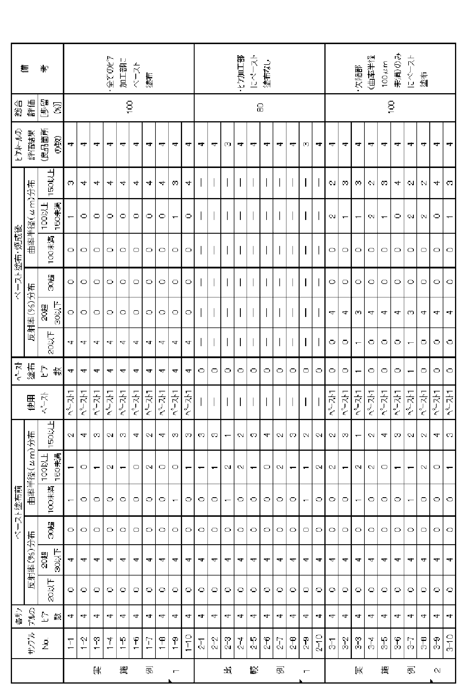

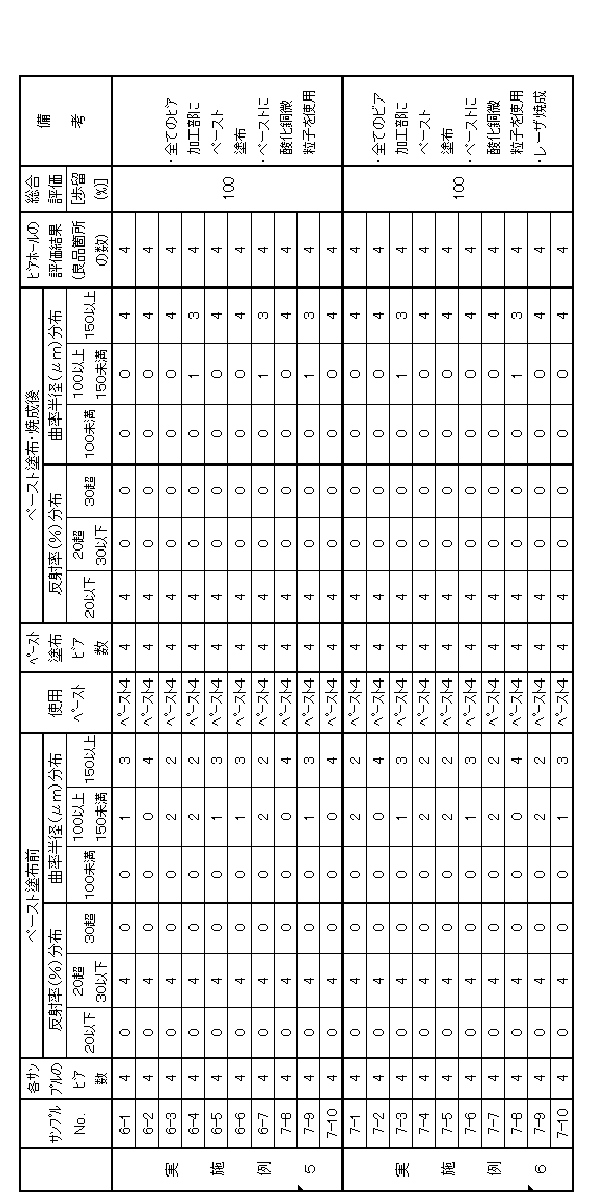
1 ガラスエポキシ樹脂
2 銅箔
3 ビルドアップ樹脂
4 銅めっき部
5 金属微粒子集合体層
11 ビアホール部
12 欠陥部
2 銅箔
3 ビルドアップ樹脂
4 銅めっき部
5 金属微粒子集合体層
11 ビアホール部
12 欠陥部
Claims (11)
- ビルドアップ多層基板の製造方法であって、
絶縁層表面に銅箔又は銅パターン層を積層したビルドアップ層(L1)に形成されたビア導体(B1)表面上に、金属微粒子を含むペーストを塗布後加熱して、金属微粒子集合体層(S1)を形成する工程(工程1)と、
ビルドアップ層(L1)上に形成され、絶縁層表面に銅箔又は銅パターン層が積層されたビルドアップ層(L2)表面から金属微粒子集合体層(S1)部にレーザー照射を行って、層間接続用ビアホール(V2)を形成する工程(工程2)を含むことを特徴とする、ビルドアップ多層基板の製造方法。 - 前記金属微粒子集合体層(S1)におけるレーザー照射部表面の、レーザー光の0.2~11.0μmの波長範囲における反射率、又は前記ビアホール(V2)形成に使用するレーザー光の波長における反射率が20%以下であることを特徴とする、請求項1に記載のビルドアップ多層基板の製造方法。
- 前記金属微粒子集合体層(S1)におけるレーザー照射部表面の曲率半径が100μm以上であることを特徴とする、請求項1に記載のビルドアップ多層基板の製造方法。
- 前記ビア導体(B1)が、前記ビルドアップ層(L1)に形成された層間ビアホール(V1)にビアフィルめっき、又はビアフィルめっき後に研磨を行って形成された導体であることを特徴とする、請求項1から3のいずれかに記載のビルドアップ多層基板の製造方法。
- 前記工程2で形成された、ビルドアップ層(L2)の層間接続用ビアホール(V2)にビアフィルめっき、又はビアフィルめっき後研磨を行ってビア導体(B2)を形成し(工程1’)、
更に前記工程1と工程2を、1回又は2回以上繰り返し行ってビルドアップ層(L)を積層することを特徴とする、請求項1から4のいずれかに記載のビルドアップ多層基板の製造方法。 - 前記工程2のビルドアップ層(L1)が基板上に形成されていることを特徴とする、請求項1から5のいずれかに記載のビルドアップ多層基板の製造方法。
- 前記工程1で形成されるいずれかの金属微粒子集合体層(S1)のレーザー照射部表面のレーザー光反射率が、ビアフィルめっき後、又はビアフィルめっき・研磨後の、レーザー照射部に対応するめっき表面のレーザー光反射率より低下していることを特徴とする、請求項1から6のいずれかに記載の多層基板の製造方法。
- 前記工程1で形成されるいずれかの金属微粒子集合体層(S1)におけるレーザー照射部表面の、レーザー光の0.2~11.0μmの波長範囲でのレーザー光反射率が15%以下であることを特徴とする、請求項1から7のいずれかに記載のビルドアップ多層基板の製造方法。
- 前記工程1で使用するペースト中の金属微粒子が銅、又は銅合金であることを特徴とする、請求項1から8のいずれかに記載のビルドアップ多層基板の製造方法。
- 絶縁層表面に銅パターン層が積層されたビルドアップ層(L)に、レーザー加工により形成された層間接続用ビアホール(V)にビアフィルめっきによりビア導体(B)が形成され、該めっき表面上に更に金属微粒子集合体層(S)が形成されたビルドアップ層(L)を少なくとも1層含む、厚み方向に隣接する一対のビア導体(B)同士が連続して接続している構造(ビアオンビア構造)であることを特徴とする、ビルドアップ多層基板。
- 前記金属微粒子集合体層(S)における金属微粒子の平均粒径が10~300nmであることを特徴とする、請求項10に記載のビルドアップ多層基板。
Priority Applications (1)
| Application Number | Priority Date | Filing Date | Title |
|---|---|---|---|
| JP2014545730A JP5840304B2 (ja) | 2012-11-09 | 2013-11-06 | ビルドアップ多層基板の製造方法、及びビルドアップ多層基板 |
Applications Claiming Priority (4)
| Application Number | Priority Date | Filing Date | Title |
|---|---|---|---|
| JP2012247094 | 2012-11-09 | ||
| JP2012-247094 | 2012-11-09 | ||
| JP2012249231 | 2012-11-13 | ||
| JP2012-249231 | 2012-11-13 |
Publications (1)
| Publication Number | Publication Date |
|---|---|
| WO2014073563A1 true WO2014073563A1 (ja) | 2014-05-15 |
Family
ID=50684665
Family Applications (1)
| Application Number | Title | Priority Date | Filing Date |
|---|---|---|---|
| PCT/JP2013/080006 Ceased WO2014073563A1 (ja) | 2012-11-09 | 2013-11-06 | ビルドアップ多層基板の製造方法、及びビルドアップ多層基板 |
Country Status (3)
| Country | Link |
|---|---|
| JP (1) | JP5840304B2 (ja) |
| TW (1) | TWI618464B (ja) |
| WO (1) | WO2014073563A1 (ja) |
Cited By (1)
| Publication number | Priority date | Publication date | Assignee | Title |
|---|---|---|---|---|
| JPWO2021166139A1 (ja) * | 2020-02-20 | 2021-08-26 |
Citations (7)
| Publication number | Priority date | Publication date | Assignee | Title |
|---|---|---|---|---|
| JPH11300487A (ja) * | 1998-04-20 | 1999-11-02 | Sony Corp | 孔加工方法及び孔加工体 |
| JP2005136048A (ja) * | 2003-10-29 | 2005-05-26 | Kyocera Corp | 多層配線基板の製造方法 |
| JP2009010266A (ja) * | 2007-06-29 | 2009-01-15 | Meiko:Kk | プリント配線板の製造方法及びプリント配線板 |
| JP2009188146A (ja) * | 2008-02-06 | 2009-08-20 | Murata Mfg Co Ltd | 配線基板の製造方法 |
| JP2009188218A (ja) * | 2008-02-07 | 2009-08-20 | Murata Mfg Co Ltd | 多層基板 |
| JP2012028456A (ja) * | 2010-07-21 | 2012-02-09 | Murata Mfg Co Ltd | セラミック電子部品の製造方法、セラミック電子部品及び配線基板 |
| JP2012156525A (ja) * | 2005-07-07 | 2012-08-16 | Ibiden Co Ltd | 多層プリント配線板 |
-
2013
- 2013-11-05 TW TW102140070A patent/TWI618464B/zh not_active IP Right Cessation
- 2013-11-06 JP JP2014545730A patent/JP5840304B2/ja not_active Expired - Fee Related
- 2013-11-06 WO PCT/JP2013/080006 patent/WO2014073563A1/ja not_active Ceased
Patent Citations (7)
| Publication number | Priority date | Publication date | Assignee | Title |
|---|---|---|---|---|
| JPH11300487A (ja) * | 1998-04-20 | 1999-11-02 | Sony Corp | 孔加工方法及び孔加工体 |
| JP2005136048A (ja) * | 2003-10-29 | 2005-05-26 | Kyocera Corp | 多層配線基板の製造方法 |
| JP2012156525A (ja) * | 2005-07-07 | 2012-08-16 | Ibiden Co Ltd | 多層プリント配線板 |
| JP2009010266A (ja) * | 2007-06-29 | 2009-01-15 | Meiko:Kk | プリント配線板の製造方法及びプリント配線板 |
| JP2009188146A (ja) * | 2008-02-06 | 2009-08-20 | Murata Mfg Co Ltd | 配線基板の製造方法 |
| JP2009188218A (ja) * | 2008-02-07 | 2009-08-20 | Murata Mfg Co Ltd | 多層基板 |
| JP2012028456A (ja) * | 2010-07-21 | 2012-02-09 | Murata Mfg Co Ltd | セラミック電子部品の製造方法、セラミック電子部品及び配線基板 |
Cited By (2)
| Publication number | Priority date | Publication date | Assignee | Title |
|---|---|---|---|---|
| JPWO2021166139A1 (ja) * | 2020-02-20 | 2021-08-26 | ||
| WO2021166139A1 (ja) * | 2020-02-20 | 2021-08-26 | 株式会社Fuji | 回路形成方法 |
Also Published As
| Publication number | Publication date |
|---|---|
| TW201433236A (zh) | 2014-08-16 |
| JPWO2014073563A1 (ja) | 2016-09-08 |
| JP5840304B2 (ja) | 2016-01-06 |
| TWI618464B (zh) | 2018-03-11 |
Similar Documents
| Publication | Publication Date | Title |
|---|---|---|
| TW507507B (en) | Liquid thermosetting resin composition, printed wiring boards and process for their production | |
| JP2008508703A (ja) | 電子回路アセンブリの製造方法 | |
| US8756803B2 (en) | Method for manufacturing printed wiring board | |
| KR101489206B1 (ko) | 도금층을 포함하는 양면 연성 인쇄회로기판 및 이의 제조방법 | |
| JP2011060824A (ja) | 半導体チップ搭載用基板及びその製造方法 | |
| JP2009065008A (ja) | 導電性ペースト組成物 | |
| CN110972403A (zh) | 一种基于纳米铜的精细嵌入式线路的成型方法 | |
| JP2014143237A (ja) | ビアホールの形成方法及び多層プリント配線板の製造方法 | |
| JP5840304B2 (ja) | ビルドアップ多層基板の製造方法、及びビルドアップ多層基板 | |
| JP2024035133A (ja) | 貫通ビア金属配線の形成方法 | |
| TWI327452B (en) | Process for manufacturing a wiring substrate | |
| CN111575752A (zh) | 一种pcb中深微孔的电镀制作方法 | |
| JP2013093359A (ja) | 半導体チップ搭載用基板及びその製造方法 | |
| CN107926116A (zh) | 印刷线路板和电子部件 | |
| CN120499940A (zh) | 一种pcb的制备方法及应用 | |
| JP5938948B2 (ja) | 半導体チップ搭載用基板及びその製造方法 | |
| JPH11126974A (ja) | 多層配線板の製造方法 | |
| JP2018029139A (ja) | プリント配線板用基板及びプリント配線板用基板の製造方法 | |
| JP3944493B2 (ja) | プリント配線板及びその製造方法並びに多層プリント配線板 | |
| JP2000036661A (ja) | ビルドアップ多層配線板の製造方法 | |
| JP2001015934A (ja) | 多層プリント配線板及びその製造方法 | |
| TWI403239B (zh) | 油墨及利用該油墨製作導電線路之方法 | |
| JP3981314B2 (ja) | 多層配線基板の製造方法 | |
| JP2011023428A (ja) | 複合体の製造方法及び複合体 | |
| JP2006019654A (ja) | 多層配線板およびその製造方法 |
Legal Events
| Date | Code | Title | Description |
|---|---|---|---|
| 121 | Ep: the epo has been informed by wipo that ep was designated in this application |
Ref document number: 13852374 Country of ref document: EP Kind code of ref document: A1 |
|
| ENP | Entry into the national phase |
Ref document number: 2014545730 Country of ref document: JP Kind code of ref document: A |
|
| NENP | Non-entry into the national phase |
Ref country code: DE |
|
| 122 | Ep: pct application non-entry in european phase |
Ref document number: 13852374 Country of ref document: EP Kind code of ref document: A1 |